EP1930968B1 - Organic light emitting display apparatus - Google Patents
Organic light emitting display apparatus Download PDFInfo
- Publication number
- EP1930968B1 EP1930968B1 EP07254721.9A EP07254721A EP1930968B1 EP 1930968 B1 EP1930968 B1 EP 1930968B1 EP 07254721 A EP07254721 A EP 07254721A EP 1930968 B1 EP1930968 B1 EP 1930968B1
- Authority
- EP
- European Patent Office
- Prior art keywords
- light emitting
- organic light
- emitting display
- display apparatus
- electrode
- Prior art date
- Legal status (The legal status is an assumption and is not a legal conclusion. Google has not performed a legal analysis and makes no representation as to the accuracy of the status listed.)
- Active
Links
- 238000002161 passivation Methods 0.000 claims description 34
- 238000007789 sealing Methods 0.000 claims description 25
- 239000000758 substrate Substances 0.000 claims description 25
- 230000003287 optical effect Effects 0.000 claims description 23
- 238000002834 transmittance Methods 0.000 claims description 22
- 239000011159 matrix material Substances 0.000 claims description 18
- 229910052751 metal Inorganic materials 0.000 claims description 11
- 239000002184 metal Substances 0.000 claims description 11
- OKTJSMMVPCPJKN-UHFFFAOYSA-N Carbon Chemical compound [C] OKTJSMMVPCPJKN-UHFFFAOYSA-N 0.000 claims description 7
- 229910052737 gold Inorganic materials 0.000 claims description 5
- 229910052709 silver Inorganic materials 0.000 claims description 5
- 239000000084 colloidal system Substances 0.000 claims description 4
- 229910002804 graphite Inorganic materials 0.000 claims description 4
- 239000010439 graphite Substances 0.000 claims description 4
- 229910052799 carbon Inorganic materials 0.000 claims description 3
- 239000011347 resin Substances 0.000 claims description 3
- 229920005989 resin Polymers 0.000 claims description 3
- 229920001187 thermosetting polymer Polymers 0.000 claims description 3
- 229910003460 diamond Inorganic materials 0.000 claims description 2
- 239000010432 diamond Substances 0.000 claims description 2
- 239000003822 epoxy resin Substances 0.000 claims description 2
- UHESRSKEBRADOO-UHFFFAOYSA-N ethyl carbamate;prop-2-enoic acid Chemical compound OC(=O)C=C.CCOC(N)=O UHESRSKEBRADOO-UHFFFAOYSA-N 0.000 claims description 2
- 229920000647 polyepoxide Polymers 0.000 claims description 2
- 239000010410 layer Substances 0.000 description 88
- 239000010408 film Substances 0.000 description 77
- 229920000642 polymer Polymers 0.000 description 13
- 238000000034 method Methods 0.000 description 9
- VYPSYNLAJGMNEJ-UHFFFAOYSA-N Silicium dioxide Chemical compound O=[Si]=O VYPSYNLAJGMNEJ-UHFFFAOYSA-N 0.000 description 8
- 239000011368 organic material Substances 0.000 description 7
- 239000000463 material Substances 0.000 description 6
- 239000004065 semiconductor Substances 0.000 description 5
- 229910052681 coesite Inorganic materials 0.000 description 4
- 229910052906 cristobalite Inorganic materials 0.000 description 4
- 239000000377 silicon dioxide Substances 0.000 description 4
- 238000004528 spin coating Methods 0.000 description 4
- 229910052682 stishovite Inorganic materials 0.000 description 4
- 239000012780 transparent material Substances 0.000 description 4
- 229910052905 tridymite Inorganic materials 0.000 description 4
- 229910052779 Neodymium Inorganic materials 0.000 description 3
- 229910004205 SiNX Inorganic materials 0.000 description 3
- 229910052782 aluminium Inorganic materials 0.000 description 3
- 229910052804 chromium Inorganic materials 0.000 description 3
- 239000011248 coating agent Substances 0.000 description 3
- 238000000576 coating method Methods 0.000 description 3
- PJXISJQVUVHSOJ-UHFFFAOYSA-N indium(III) oxide Inorganic materials [O-2].[O-2].[O-2].[In+3].[In+3] PJXISJQVUVHSOJ-UHFFFAOYSA-N 0.000 description 3
- 229910052741 iridium Inorganic materials 0.000 description 3
- 229910052744 lithium Inorganic materials 0.000 description 3
- 229910052749 magnesium Inorganic materials 0.000 description 3
- 229910052759 nickel Inorganic materials 0.000 description 3
- 229910052763 palladium Inorganic materials 0.000 description 3
- 229910052697 platinum Inorganic materials 0.000 description 3
- YTPLMLYBLZKORZ-UHFFFAOYSA-N Thiophene Chemical compound C=1C=CSC=1 YTPLMLYBLZKORZ-UHFFFAOYSA-N 0.000 description 2
- GWEVSGVZZGPLCZ-UHFFFAOYSA-N Titan oxide Chemical compound O=[Ti]=O GWEVSGVZZGPLCZ-UHFFFAOYSA-N 0.000 description 2
- MCMNRKCIXSYSNV-UHFFFAOYSA-N Zirconium dioxide Chemical compound O=[Zr]=O MCMNRKCIXSYSNV-UHFFFAOYSA-N 0.000 description 2
- 238000000137 annealing Methods 0.000 description 2
- 229910052791 calcium Inorganic materials 0.000 description 2
- 238000005229 chemical vapour deposition Methods 0.000 description 2
- 150000001875 compounds Chemical class 0.000 description 2
- 238000003618 dip coating Methods 0.000 description 2
- 239000011521 glass Substances 0.000 description 2
- 238000002347 injection Methods 0.000 description 2
- 239000007924 injection Substances 0.000 description 2
- 238000007641 inkjet printing Methods 0.000 description 2
- 239000011810 insulating material Substances 0.000 description 2
- 150000002739 metals Chemical class 0.000 description 2
- 150000002894 organic compounds Chemical class 0.000 description 2
- 229920003023 plastic Polymers 0.000 description 2
- 229920000767 polyaniline Polymers 0.000 description 2
- VYZAMTAEIAYCRO-UHFFFAOYSA-N Chromium Chemical compound [Cr] VYZAMTAEIAYCRO-UHFFFAOYSA-N 0.000 description 1
- KRHYYFGTRYWZRS-UHFFFAOYSA-M Fluoride anion Chemical compound [F-] KRHYYFGTRYWZRS-UHFFFAOYSA-M 0.000 description 1
- UFHFLCQGNIYNRP-UHFFFAOYSA-N Hydrogen Chemical compound [H][H] UFHFLCQGNIYNRP-UHFFFAOYSA-N 0.000 description 1
- 239000004793 Polystyrene Substances 0.000 description 1
- -1 acryl Chemical group 0.000 description 1
- PNEYBMLMFCGWSK-UHFFFAOYSA-N aluminium oxide Inorganic materials [O-2].[O-2].[O-2].[Al+3].[Al+3] PNEYBMLMFCGWSK-UHFFFAOYSA-N 0.000 description 1
- 150000001408 amides Chemical class 0.000 description 1
- 229910021417 amorphous silicon Inorganic materials 0.000 description 1
- 150000007860 aryl ester derivatives Chemical class 0.000 description 1
- QVGXLLKOCUKJST-UHFFFAOYSA-N atomic oxygen Chemical compound [O] QVGXLLKOCUKJST-UHFFFAOYSA-N 0.000 description 1
- 229910052454 barium strontium titanate Inorganic materials 0.000 description 1
- 230000015572 biosynthetic process Effects 0.000 description 1
- 230000015556 catabolic process Effects 0.000 description 1
- 239000002131 composite material Substances 0.000 description 1
- 239000004020 conductor Substances 0.000 description 1
- 238000007796 conventional method Methods 0.000 description 1
- 229910052593 corundum Inorganic materials 0.000 description 1
- 238000006731 degradation reaction Methods 0.000 description 1
- 238000000151 deposition Methods 0.000 description 1
- 230000009977 dual effect Effects 0.000 description 1
- 238000000605 extraction Methods 0.000 description 1
- CJNBYAVZURUTKZ-UHFFFAOYSA-N hafnium(IV) oxide Inorganic materials O=[Hf]=O CJNBYAVZURUTKZ-UHFFFAOYSA-N 0.000 description 1
- RBTKNAXYKSUFRK-UHFFFAOYSA-N heliogen blue Chemical compound [Cu].[N-]1C2=C(C=CC=C3)C3=C1N=C([N-]1)C3=CC=CC=C3C1=NC([N-]1)=C(C=CC=C3)C3=C1N=C([N-]1)C3=CC=CC=C3C1=N2 RBTKNAXYKSUFRK-UHFFFAOYSA-N 0.000 description 1
- 230000005525 hole transport Effects 0.000 description 1
- 229910052739 hydrogen Inorganic materials 0.000 description 1
- 239000001257 hydrogen Substances 0.000 description 1
- 150000003949 imides Chemical class 0.000 description 1
- 229910010272 inorganic material Inorganic materials 0.000 description 1
- 239000011147 inorganic material Substances 0.000 description 1
- 239000011229 interlayer Substances 0.000 description 1
- 229910052451 lead zirconate titanate Inorganic materials 0.000 description 1
- 238000001465 metallisation Methods 0.000 description 1
- 239000000203 mixture Substances 0.000 description 1
- IBHBKWKFFTZAHE-UHFFFAOYSA-N n-[4-[4-(n-naphthalen-1-ylanilino)phenyl]phenyl]-n-phenylnaphthalen-1-amine Chemical compound C1=CC=CC=C1N(C=1C2=CC=CC=C2C=CC=1)C1=CC=C(C=2C=CC(=CC=2)N(C=2C=CC=CC=2)C=2C3=CC=CC=C3C=CC=2)C=C1 IBHBKWKFFTZAHE-UHFFFAOYSA-N 0.000 description 1
- 229910052760 oxygen Inorganic materials 0.000 description 1
- 239000001301 oxygen Substances 0.000 description 1
- 230000000149 penetrating effect Effects 0.000 description 1
- ISWSIDIOOBJBQZ-UHFFFAOYSA-N phenol group Chemical group C1(=CC=CC=C1)O ISWSIDIOOBJBQZ-UHFFFAOYSA-N 0.000 description 1
- 238000000206 photolithography Methods 0.000 description 1
- 239000004033 plastic Substances 0.000 description 1
- 239000002985 plastic film Substances 0.000 description 1
- 229920006255 plastic film Polymers 0.000 description 1
- 229920003229 poly(methyl methacrylate) Polymers 0.000 description 1
- 229910021420 polycrystalline silicon Inorganic materials 0.000 description 1
- 229920002098 polyfluorene Polymers 0.000 description 1
- 239000004926 polymethyl methacrylate Substances 0.000 description 1
- 229920005591 polysilicon Polymers 0.000 description 1
- 229920002223 polystyrene Polymers 0.000 description 1
- 229920002451 polyvinyl alcohol Polymers 0.000 description 1
- 235000012239 silicon dioxide Nutrition 0.000 description 1
- 229910052814 silicon oxide Inorganic materials 0.000 description 1
- 238000004544 sputter deposition Methods 0.000 description 1
- PBCFLUZVCVVTBY-UHFFFAOYSA-N tantalum pentoxide Inorganic materials O=[Ta](=O)O[Ta](=O)=O PBCFLUZVCVVTBY-UHFFFAOYSA-N 0.000 description 1
- 239000010409 thin film Substances 0.000 description 1
- 229930192474 thiophene Natural products 0.000 description 1
- TVIVIEFSHFOWTE-UHFFFAOYSA-K tri(quinolin-8-yloxy)alumane Chemical compound [Al+3].C1=CN=C2C([O-])=CC=CC2=C1.C1=CN=C2C([O-])=CC=CC2=C1.C1=CN=C2C([O-])=CC=CC2=C1 TVIVIEFSHFOWTE-UHFFFAOYSA-K 0.000 description 1
- 229910001845 yogo sapphire Inorganic materials 0.000 description 1
Images

Classifications
-
- H—ELECTRICITY
- H10—SEMICONDUCTOR DEVICES; ELECTRIC SOLID-STATE DEVICES NOT OTHERWISE PROVIDED FOR
- H10K—ORGANIC ELECTRIC SOLID-STATE DEVICES
- H10K50/00—Organic light-emitting devices
- H10K50/80—Constructional details
- H10K50/86—Arrangements for improving contrast, e.g. preventing reflection of ambient light
-
- H—ELECTRICITY
- H05—ELECTRIC TECHNIQUES NOT OTHERWISE PROVIDED FOR
- H05B—ELECTRIC HEATING; ELECTRIC LIGHT SOURCES NOT OTHERWISE PROVIDED FOR; CIRCUIT ARRANGEMENTS FOR ELECTRIC LIGHT SOURCES, IN GENERAL
- H05B33/00—Electroluminescent light sources
- H05B33/02—Details
- H05B33/04—Sealing arrangements, e.g. against humidity
-
- H—ELECTRICITY
- H05—ELECTRIC TECHNIQUES NOT OTHERWISE PROVIDED FOR
- H05B—ELECTRIC HEATING; ELECTRIC LIGHT SOURCES NOT OTHERWISE PROVIDED FOR; CIRCUIT ARRANGEMENTS FOR ELECTRIC LIGHT SOURCES, IN GENERAL
- H05B33/00—Electroluminescent light sources
- H05B33/12—Light sources with substantially two-dimensional radiating surfaces
- H05B33/22—Light sources with substantially two-dimensional radiating surfaces characterised by the chemical or physical composition or the arrangement of auxiliary dielectric or reflective layers
-
- H—ELECTRICITY
- H10—SEMICONDUCTOR DEVICES; ELECTRIC SOLID-STATE DEVICES NOT OTHERWISE PROVIDED FOR
- H10K—ORGANIC ELECTRIC SOLID-STATE DEVICES
- H10K50/00—Organic light-emitting devices
- H10K50/80—Constructional details
- H10K50/84—Passivation; Containers; Encapsulations
- H10K50/841—Self-supporting sealing arrangements
-
- H—ELECTRICITY
- H10—SEMICONDUCTOR DEVICES; ELECTRIC SOLID-STATE DEVICES NOT OTHERWISE PROVIDED FOR
- H10K—ORGANIC ELECTRIC SOLID-STATE DEVICES
- H10K50/00—Organic light-emitting devices
- H10K50/80—Constructional details
- H10K50/86—Arrangements for improving contrast, e.g. preventing reflection of ambient light
- H10K50/865—Arrangements for improving contrast, e.g. preventing reflection of ambient light comprising light absorbing layers, e.g. light-blocking layers
-
- H—ELECTRICITY
- H10—SEMICONDUCTOR DEVICES; ELECTRIC SOLID-STATE DEVICES NOT OTHERWISE PROVIDED FOR
- H10K—ORGANIC ELECTRIC SOLID-STATE DEVICES
- H10K59/00—Integrated devices, or assemblies of multiple devices, comprising at least one organic light-emitting element covered by group H10K50/00
- H10K59/10—OLED displays
- H10K59/12—Active-matrix OLED [AMOLED] displays
-
- H—ELECTRICITY
- H10—SEMICONDUCTOR DEVICES; ELECTRIC SOLID-STATE DEVICES NOT OTHERWISE PROVIDED FOR
- H10K—ORGANIC ELECTRIC SOLID-STATE DEVICES
- H10K59/00—Integrated devices, or assemblies of multiple devices, comprising at least one organic light-emitting element covered by group H10K50/00
- H10K59/30—Devices specially adapted for multicolour light emission
- H10K59/38—Devices specially adapted for multicolour light emission comprising colour filters or colour changing media [CCM]
Landscapes
- Physics & Mathematics (AREA)
- Optics & Photonics (AREA)
- Electroluminescent Light Sources (AREA)
- Devices For Indicating Variable Information By Combining Individual Elements (AREA)
Description
- The present invention relates to an organic light emitting display apparatus and more particularly, to an organic light emitting display apparatus with increased contrast and impact resistance.
- It is recent trend that display apparatuses are replaced by thin flat panel display apparatuses that can be used in mobile applications. Of the flat panel display apparatuses, organic and inorganic organic light emitting display apparatuses are expected to be next generation display apparatuses due to the advantages in that the organic and inorganic organic light emitting display apparatuses are emissive type display apparatuses and have a wide viewing angle, high contrast, and a short response time. Organic light emitting display apparatuses in which a light emitting layer is formed of an organic material have characteristics such as higher brightness, a low driving voltage, and a short response time, which are superior to those of the Inorganic light emitting display apparatus, and can also be multi-colored.
- Flat panel display apparatuses are formed to be lightweight and thin so that can be portable and be used outdoors. When a flat panel display apparatus is used outdoors, the contrast and visibility can be reduced due to the reflection of sunlight. In particular, for organic light emitting display apparatuses, the reflection of sunlight caused by a metal reflection film of the organic light emitting display apparatuses can be severe.
- Also, there is a high possibility that an external surface of the organic light emitting display apparatuses can be easily damaged by external impact.
-
US2003183830 discloses a light emitting device having an organic compound layer formed from laminated sections by means of intentionally and partially overlapping different organic compound layers of adjacent light emitting elements. -
US2003/0146446 discloses an organic light emitting display having a substrate, organic light emitting elements on the substrate and a sealing member. A diamond-like carbon layer is formed on both surfaces of a plastic film which is positioned on an opposite surface of the substrate to the organic light emitting elements. -
EP1441571 discloses an organic light emitting display having a substrate, organic light emitting elements on the substrate and a sealing panel. A colour filter is located on an internal surface of the sealing panel facing the organic light emitting elements. -
US2003/0027369 discloses an organic light emitting display having a sealing member and an inorganic insulating film. -
US2002/0030440 discloses an organic light emitting display having light emitting elements formed on a flexible film. - The present invention provides an organic light emitting display apparatus with increased contrast and impact resistance.
- According to an aspect of the present invention, there is provided an organic light emitting display apparatus as set out in Claim 1. Preferred features of this aspect are set out in Claims 2 to 10.
- The above and other features and advantages of the present invention will become more apparent by describing in detail exemplary embodiments thereof with reference to the attached drawings in which:
-
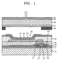
FIG. 1 is a schematic cross-sectional view illustrating an organic light emitting display apparatus according to an embodiment of the present invention; -
FIGS. 2 through 4 are schematic cross-sectional views illustrating modified versions of the organic light emitting display apparatus ofFIG. 1 , according to an embodiment of the present invention; and -
FIG. 5 is a schematic cross-sectional view illustrating an organic light emitting display apparatus according to another embodiment of the present invention. - The present invention will now be described more fully with reference to the accompanying drawings in which exemplary embodiments of the invention are shown.
-
FIG. 1 is a schematic cross-sectional view illustrating an organic light emitting display apparatus according to an embodiment of the present invention. Organic light emitting display apparatuses are largely classified as active matrix (AM) type organic light emitting display apparatuses and passive matrix (PM) type organic light emitting display apparatuses. The organic light emitting display apparatus depicted inFIG. 1 is an AM type organic light emitting display apparatus, however, embodiments of the present invention are not limited thereto and can also be a PM type organic light emitting display apparatus. - Referring to
FIG. 1 , the organic light emitting display apparatus according to an embodiment of the present invention includes asubstrate 10, an organiclight emitting device 30, asealing member 50, asemi-transparent film 51, apassivation film 52, a transmissiveblack layer 21, and ablack matrix layer 22. - The
substrate 10 can be formed of a transparent glass material having SiO2 as a main component. However, thesubstrate 10 is not limited thereto. That is, thesubstrate 10 can be formed of a transparent plastic material. In the case of a bottom emission type organic light emitting display apparatus in which an image is displayed through thesubstrate 10, thesubstrate 10 must be formed of a transparent material. However, as depicted inFIG. 1 , in the case of a top emission type organic light emitting display apparatus in which an image is displayed through thesealing member 50, thesubstrate 10 is not necessarily formed of a transparent material. - In this embodiment, a
buffer layer 11 is be formed on an upper surface of thesubstrate 10 to secure planarity of thesubstrate 10 and to prevent impure elements from penetrating into the organic light emitting display apparatus. Thebuffer layer 11 can be formed of at least one of SiO2 and SiNx. - A thin film transistor (TFT) is formed on the upper surface of the
substrate 10. At least one TFT is formed in each pixel and is electrically connected to the organiclight emitting device 30. - More specifically, a
semiconductor layer 12 having a predetermined pattern is formed on thebuffer layer 11. Thesemiconductor layer 12 can be formed of an inorganic or organic semiconductor such as an amorphous silicon or poly silicon, and includes a source region, a drain region, and a channel region. - A
gate insulating film 13 is formed of SiO2 or SiNx on an upper surface of thesemiconductor layer 12 and thebuffer layer 11, and agate electrode 14 is formed in a predetermined region on an upper surface of thegate insulating film 13. Thegate electrode 14 is connected to a gate line (not shown) that applies an ON/OFF signal to the TFT. - An
interlayer insulating layer 15 is formed on thegate electrode 14, and asource electrode 16 and adrain electrode 17 are respectively connected to the source region and the drain region of thesemiconductor layer 12 through contact holes. The TFT is protected by apassivation film 18, which can be at least one of an inorganic insulating film and an organic insulating film. The inorganic insulating film can be formed of SiO2, SiNx, SiON, Al2O3, TiO2, Ta2O5, HfO2, ZrO2, BST, or PZT. The organic insulating film can be formed of ordinary multi-purpose polymers such as polymethyl methacrylate or polystyrene, polymer derivatives having a phenol group, an acryl polymer, an imide polymer, an arylester polymer, an amide polymer, a fluoride polymer, a p-gilyrene polymer, a vinyl alcohol polymer, or a mixture of these polymers. Thepassivation film 18 can be formed as a composite stack of an inorganic insulating film and an organic insulating film. - A
first electrode 31 that functions as an anode electrode of the organiclight emitting device 30 is formed on thepassivation film 18, and apixel defining layer 36 covering thefirst electrode 31 is formed of an insulating material. After a predetermined opening is formed in thepixel defining layer 36, an organiclight emitting layer 32 of the organiclight emitting device 30 is formed in a region defined by the opening. Afterwards, asecond electrode 33 that functions as a cathode electrode of the organiclight emitting device 30 is formed to cover the entire pixel. The polarity of thefirst electrode 31 and thesecond electrode 33 may be reversed. - The organic
light emitting device 30 displays an image by emitting light according to current flow, and includes thefirst electrode 31 electrically connected to thedrain electrode 17 of the TFT through a contact hole, the organiclight emitting layer 32, and thesecond electrode 33. - The
first electrode 31 can be formed in a predetermined pattern using a photolithography method. In a PM type organic light emitting display apparatus, the pattern of thefirst electrode 31 can be formed in a stripe shape separated by a predetermined distance, and in an AM type organic light emitting display apparatus, the pattern of thefirst electrode 31 can be formed in a shape corresponding to the shape of the pixel. Thesecond electrode 33 is disposed above thefirst electrode 31, and can be used as a cathode electrode by connecting to an external terminal (not shown). In the case of a PM type organic light emitting display apparatus, thesecond electrode 33 can be formed in a stripe shape crossing the pattern of thefirst electrode 31, and in the case of the AM type organic light emitting display apparatus, thesecond electrode 33 can be formed on the entire region where an image is displayed. The polarity of thefirst electrode 31 and thesecond electrode 33 may be reversed. In the case of a bottom emission type organic light emitting display apparatus in which an image is displayed through thesubstrate 10, thefirst electrode 31 is a transparent electrode, and thesecond electrode 33 can be a reflection electrode. Thefirst electrode 31 is formed of a material having a high work function such as ITO, IZO, ZnO, or In2O3, and thesecond electrode 33 can be formed of a metal having a low work function such as Ag, Mg, Al, Pt, Pd, Au, Ni, Nd, Ir, Cr, Li, or Ca. - In the case of a top emission type organic light emitting display apparatus in which an image is displayed through the
second electrode 33, thefirst electrode 31 can be a reflection electrode and thesecond electrode 33 can be a transparent electrode. In this case, the reflection electrode that functions as thefirst electrode 31 is formed on the reflection film using a material having a high work function such as ITO, IZO, ZnO, or In2O3. The reflection film is formed using a metal such as Ag, Mg, Al, Pt, Pd, Au, Ni, Nd, Ir, Cr, Li, Ca, or compound of these metals. The transparent electrode that functions as thesecond electrodes 33 can be formed by depositing a metal such as Ag, Mg, Al, Pt, Pd, Au, Ni, Nd, Ir, Cr, Li, Ca, or a compound of these metals having a small work function and by forming an auxiliary electrode layer or a bus electrode line using a transparent conductive material such as ITO, IZO, ZnO, or In2O3 on the metal deposition. - In the case of a dual side emission type organic light emitting display apparatus, the first and
second electrodes - The organic
light emitting layer 32 that is interposed between thefirst electrode 31 and thesecond electrode 33 emits light according to electrical driving of thefirst electrode 31 and thesecond electrode 33. The organiclight emitting layer 32 can be formed of a low molecular weight organic material or a polymer organic material. When the organiclight emitting layer 32 is formed of a low molecular weight organic material, a hole transport layer (HTL) and a hole injection layer (HIL) are stacked in a direction towards thefirst electrode 31 from the organiclight emitting layer 32, and an electron transport layer (ETL) and an electron injection layer (EIL) are stacked in a direction towards thesecond electrode 33 from the organiclight emitting layer 32. Besides these layers, various other layers can be stacked if necessary. The low molecular weight organic material of the organiclight emitting layer 32 can be of various materials including copper phthalocyanine (CuPc), N,N'-Di(naphthalene-1-yl)-N,N'-diphenyl-benzidine (NPB), and tris-8-hydroxyquinoline aluminum (Alq3). - When the organic
light emitting layer 32 is formed of a polymer organic material, an HTL is formed in a direction towards thefirst electrode 31 from the organiclight emitting layer 32. The polymer HTL can be formed on thefirst electrode 31 using poly-(2,4)-ethylene-dihydroxy thiophene (PEDOT) or polyaniline (PANI) by an inkjet printing or a spin coating method. The polymer organiclight emitting layer 32 can be formed of poly-phenylenevinylene (PPV), soluble PPV's, cyano-PPV, or polyfluorene and a color pattern is formed using conventional methods such as an inkjet printing method, a spin coating method, or a thermal transcribing method using a laser. - The sealing
member 50 that seals the organiclight emitting device 30 is formed on the organiclight emitting device 30. The sealingmember 50 protects the organiclight emitting device 30 from external moisture or oxygen. In the top emission type organic light emitting display apparatus as depicted inFIG. 1 , the sealingmember 50 is formed of a transparent material. For this purpose, the top emission type organic light emitting display apparatus can be a structure in which a plurality of layers such as a glass substrate, a plastic substrate, or organic and inorganic materials are stacked. - The
semi-transparent film 51 that transmits a part of external light and reflects another part of the external light is formed on an upper surface of the sealingmember 50 facing the outside. Thesemi-transparent film 51 may be formed to have reflectance of 1.5 to 5. Thesemi-transparent film 51 can be formed in a metal colloid using a metal such as Ag, Au, or Ti. Thesemi-transparent film 51 can be easily formed by an annealing process after a metal colloid film is coated by spin coating, dip coating or bar coating. Thesemi-transparent film 51 is formed to have an optical transmittance of 40 to 80% by controlling the thickness of thesemi-transparent film 51 or the process conditions when the metal colloid is formed. Thesemi-transparent film 51 can be formed to have a thickness of 10 nm to 10 µm. If the thickness of thesemi-transparent film 51 is excessively thick, the optical transmittance of thesemi-transparent film 51 is reduced and thus, resulting in reducing the optical efficiency of light emitted from the organiclight emitting device 30. Therefore, thesemi-transparent film 51 is formed to a thickness of less than 10 µm. If the thickness of thesemi-transparent film 51 is excessively thin, the optical transmittance of thesemi-transparent film 51 excessively increases. Thus, external light can pass through thesemi-transparent film 51, and as a result, the amount of external light to be reflected by the reflection electrode increases. - The
passivation film 52 is formed on thesemi-transparent film 51. Thepassivation film 52 is formed to have a refractive index that is less than that of thesemi-transparent film 51. Thepassivation film 52 is formed of a thermosetting resin having high impact resistance, such as urethane acrylate or epoxy resin. Thus, thepassivation film 52 is transparent. More specifically, thepassivation film 52 can be formed by a hardening process using annealing or ultraviolet rays after coating a film by spin coating, dip coating or bar coating. Thepassivation film 52 can be formed to a thickness of 10 nm to 30 µm in some embodiments. Thepassivation film 52 is formed to a thickness of 10 nm or more to secure impact resistance in some embodiments. However, if the thickness is excessively thick, an overall thickness of the organic light emitting display apparatus increases. Therefore in some embodiments, thepassivation film 52 is formed to a thickness of 30 µm or less. - The
passivation film 52 is formed of a thermosetting resin with high impact resistance and able to protect the thinsemi-transparent film 51 from external impact. - The organic light emitting display apparatus according to this embodiment of the present embodiment has a structure in which the
semi-transparent film 51 and thepassivation film 52 are formed as an overlapping structure on the sealingmember 50 and thesemi-transparent film 51 has a refractive index greater than that of thepassivation film 52, thereby preventing the reflection of external light at an interface of thepassivation film 52. That is, the combination of thesemi-transparent film 51 and thepassivation film 52 can function as a conventional circular polarizer. In particular, the optical transmittance of the organic light emitting display apparatus according to this embodiment of the present embodiment can easily match the optical transmittance of a conventional circular polarizer by combining thesemi-transparent film 51 having an optical transmittance of 40 to 80% and thepassivation film 52 that is formed of a transparent material. - The transmissive
black layer 21 is formed between the sealingmember 50 and the organiclight emitting device 30. Referring toFIG. 1 , the transmissiveblack layer 21 is formed on a surface of the sealingmember 50 facing the organiclight emitting device 30. The transmissiveblack layer 21 can be formed of graphite or diamond like carbon (DLC) at a temperature of 250°C or less to prevent the transmissiveblack layer 21 and organiclight emitting device 30 from degradation using a sputtering method or a chemical vapor deposition (CVD) method. - The transmissive
black layer 21 is a partially transmissive layer that increases contrast of the organic light emitting display apparatus. In order to increase contrast of the organic light emitting display apparatus, the transmissiveblack layer 21 must have an appropriate optical transmittance. A low optical transmittance is advantageous for increasing contrast of the organic light emitting display apparatus. However, a low optical transmittance reduces the extraction rate of light generated from the organiclight emitting device 30. In particular, the optical transmittances of thesemi-transparent film 51 and thepassivation film 52 must also be considered. In some embodiments of the invention the transmissiveblack layer 21 is formed to have an optical transmittance of 35 to 80%. As a result of this, the optical transmittance of the organic light emitting display apparatus according to the present embodiment can be controlled from 40 to 60% even when the transmissiveblack layer 21, thesemi-transparent film 51, and thepassivation film 52 are simultaneously used. That is the organic light emitting display apparatus according to the present embodiment can prevent reflection of external light and can increase contrast while maintaining an optical transmittance of approximately 40%, which is the optical transmittance of a conventional circular polarizer, or higher even when the transmissiveblack layer 21, thesemi-transparent film 51, and thepassivation film 52 are simultaneously used. The transmissiveblack layer 21 can include 5 to 35% hydrogen so that the transmissiveblack layer 21 that is formed of graphite or DLC can have a desired optical transmittance. - The desired optical transmittance of the organic light emitting display apparatus can be obtained by controlling the thickness of the transmissive
black layer 21. Thus, in order to increase the optical transmittance of the organic light emitting display apparatus, the thickness of the transmissiveblack layer 21 is increased, and in order to reduce the optical transmittance of the organic light emitting display apparatus, the thickness of the transmissiveblack layer 21 is reduced. In some embodiments of the invention, the transmissiveblack layer 21 having a desired optical transmittance can be obtained by forming the transmissiveblack layer 21 to a thickness of 5 to 70 nm. - The transmissive
black layer 21 having an appropriate thickness can be formed by considering conditions of using thesemi-transparent film 51, thepassivation film 52, and the organic light emitting display apparatus according to the present embodiment. - The contrast of the organic light emitting display apparatus according to the present embodiment can further increase due to the formation of the transmissive
black layer 21. - The
black matrix layer 22 can be formed on the transmissiveblack layer 21. Theblack matrix layer 22 is patterned to be disposed in a non-display region of the organiclight emitting device 30. Theblack matrix layer 22 comprises a plurality of light absorbing portions formed in regions corresponding to non-display regions of the organic light emitting device. A display region of the organiclight emitting device 30 is a region where the organiclight emitting layer 32 is located, and the non-display region of the organiclight emitting device 30 is the rest regions where the organiclight emitting layer 32 is not located. Theblack matrix layer 22 can be formed of graphite or chrome having a strong dark color in order to absorb external light, however, theblack matrix layer 22 can also be formed of any material that can absorb external light. - The organic light emitting display apparatus according to the present embodiment includes the
semi-transparent film 51 and thepassivation film 52 having a refractive index lower than that of thesemi-transparent film 51 and having a high impact resistance on the sealingmember 50. Thus, the reflection of external light, in particular, at an interface of thesubstrate 10 can be reduced and an external surface of the organic light emitting display apparatus can be protected from external impact. - Also, the transmissive
black layer 21 is formed between the organiclight emitting device 30 and the sealingmember 50 in order to control the optical transmittance of the organic light emitting display apparatus, thereby increasing contrast of the organic light emitting display apparatus. The contrast of the organic light emitting display apparatus can be further increased by forming theblack matrix layer 22 in the non-display region of the organiclight emitting device 30. -
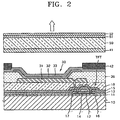
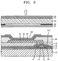
FIGS. 2 through 4 are schematic cross-sectional views illustrating modified versions of the organic light emitting display apparatus ofFIG. 1 , according to other embodiments of the present invention. Hereinafter, the differences from the organic light emitting display apparatus ofFIG. 1 will be mainly described. Like reference numerals are used to indicate elements that are substantially identical to the elements ofFIG. 1 . - Referring to
FIG. 2 , the organic light emitting display apparatus according to the present embodiment includes thesubstrate 10, the organiclight emitting device 30, the sealingmember 50, thesemi-transparent film 51, thepassivation film 52, a transmissiveblack layer 41, and ablack matrix layer 42. The transmissiveblack layer 41 is formed on a surface of the sealingmember 50 facing the organiclight emitting device 30. Theblack matrix layer 42 is formed on thesecond electrode 33. The rest of the structure is identical to the organic light emitting display apparatus ofFIG. 1 , and thus, the detailed description thereof will not be repeated. - Referring to
FIG. 3 , the organic light emitting display apparatus according to the present embodiment includes thesubstrate 10, the organiclight emitting device 30, the sealingmember 50, thesemi-transparent film 51, thepassivation film 52, a transmissiveblack layer 61, and ablack matrix layer 62. Theblack matrix layer 62 and the transmissiveblack layer 61 are sequentially formed on a surface of the sealingmember 50 facing the organiclight emitting device 30. In detail, theblack matrix layer 62 is formed between the sealingmember 50 and the transmissiveblack layer 61. - Referring to
FIG. 4 , the organic light emitting display apparatus according to the present embodiment includes thesubstrate 10, the organiclight emitting device 30, the sealingmember 50, thesemi-transparent film 51, thepassivation film 52, a transmissiveblack layer 71, and ablack matrix layer 72. The transmissiveblack layer 71 is formed on thesecond electrode 33 of the organiclight emitting device 30. The patternedblack matrix layer 72 is formed on the transmissiveblack layer 71. -
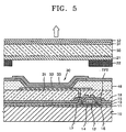
FIG. 5 is a schematic cross-sectional view illustrating an organic light emitting display apparatus according to another embodiment of the present invention. The differences between the an organic light emitting display apparatus ofFIG. 5 and the organic light emitting display apparatus ofFIG. 1 will be mainly described. Like reference numerals are used to indicate elements that are substantially identical to the elements ofFIG. 1 . - Referring to
FIG. 5 , the organic light emitting display apparatus according to the present embodiment includes asubstrate 10, an organiclight emitting device 30, a sealingmember 50, asemi-transparent film 51, apassivation film 52, apixel defining film 46, a transmissiveblack layer 21, and ablack matrix layer 22. - A
first electrode 31 that functions as an anode electrode of the organic. light emittingdevice 30 is formed on apassivation film 18, and thepixel defining layer 46 covering thepassivation film 18 is formed using an insulating material. After forming a predetermined opening in thepixel defining layer 46, an organiclight emitting layer 32 of the organiclight emitting device 30 is formed in a region defined by the opening. Afterwards, asecond electrode 33 that functions as a cathode electrode of the organiclight emitting device 30 is formed to cover the entire pixels. The polarity of thefirst electrode 31 and thesecond electrode 33 may be reversed. Thepixel defining layer 46 can be formed to have a strong dark color as an insulating layer, and in this case, the reflection of external light can be minimized, thereby increasing contrast of the organic light emitting display apparatus. In other words, thepixel defining layer 46 acts as an insulating film that absorbs light. - The organic light emitting display apparatus of
FIG. 5 can also be modified as the organic light emitting display apparatus ofFIG. 1 is modified as illustrated inFIGS. 2 through 4 . - An organic light emitting display apparatus according to the present invention has increased contrast.
- While the present invention has been particularly shown and described with reference to exemplary embodiments thereof, it will be understood by one of ordinary skill in the art that various changes in form and details may be made therein without departing from the scope of the present invention as defined by the following claims.
Claims (10)
- An organic light emitting display apparatus comprising:a substrate (10);an organic light emitting device (30) disposed over the substrate (10);a sealing member (50) formed over the organic light emitting device (30);anda partially transmissive layer (21, 41, 61, 71) formed between the sealing member (50) and the organic light emitting device (30), the partially transmissive layer (21, 41, 61) being arranged to increase contrast of images displayed by the organic light emitting display (30);characterised by:a semitransparent film (51) formed over an upper surface of the sealing member (50), the semitransparent film (51) being arranged to transmit a portion of external light and to reflect another portion of external light; anda passivation film (52) formed over the semitransparent film so as to cover the semitransparent film, the passivation film (52) being arranged to protect the semitransparent film (51);wherein the partially transmissive layer (21, 41, 61) has an optical transmittance of 35 to 80%; andwherein the semitransparent film (51) has a refractive index greater than that of the passivation film (52) and an optical transmittance of 40 to 80%.
- An organic light emitting display apparatus according to claim 1, wherein the partially transmissive layer (21, 41, 61) has a thickness of 5 to 70 nm
- An organic light emitting display apparatus according to claim 1 or 2, further comprising:a light absorbing matrix layer (42, 62) having light absorbing portions formed in regions corresponding to non-display regions of the organic light emitting device.
- An organic light emitting display apparatus according to any of claims 1 to 3, wherein:the organic light emitting device comprises a first electrode (31), a second electrode (33), and an organic light emitting layer (32) formed between the first electrode (31) and the second electrode (33); the apparatus further comprising:an insulating film formed on the first electrode having an opening so as to expose the first electrode, the insulating film being arranged to absorb light.
- An organic light emitting display apparatus according to any one of claims 1 to 4, wherein the partially transmissive layer (21, 41, 61) is formed of graphite or diamond like carbon (DLC).
- An organic light emitting display apparatus according to any one of claims 1 to 5, wherein the passivation film (52) is formed of a thermosetting resin.
- An organic light emitting display apparatus according to claim 6, wherein the passivation film (52) is formed of a urethane acrylate or an epoxy resin.
- An organic light emitting display apparatus according to any one of claims 1 to 7, wherein the semitransparent film (51) has a refractive index of 1.5 to 5.0.
- An organic light emitting display apparatus according to any one of claims 1 to 8, wherein the semitransparent film (51) is formed of a metal colloid.
- An organic light emitting display apparatus according to any one of claims 1 to 9, wherein the semitransparent film (51) comprises Ag, Au, or Ti.
Applications Claiming Priority (1)
| Application Number | Priority Date | Filing Date | Title |
|---|---|---|---|
| KR1020060123371A KR100829750B1 (en) | 2006-12-06 | 2006-12-06 | Organic light emitting display apparatus |
Publications (3)
| Publication Number | Publication Date |
|---|---|
| EP1930968A2 EP1930968A2 (en) | 2008-06-11 |
| EP1930968A3 EP1930968A3 (en) | 2011-06-01 |
| EP1930968B1 true EP1930968B1 (en) | 2016-04-27 |
Family
ID=39266439
Family Applications (1)
| Application Number | Title | Priority Date | Filing Date |
|---|---|---|---|
| EP07254721.9A Active EP1930968B1 (en) | 2006-12-06 | 2007-12-06 | Organic light emitting display apparatus |
Country Status (5)
| Country | Link |
|---|---|
| US (1) | US8022616B2 (en) |
| EP (1) | EP1930968B1 (en) |
| JP (1) | JP4558763B2 (en) |
| KR (1) | KR100829750B1 (en) |
| CN (1) | CN101197390B (en) |
Families Citing this family (28)
| Publication number | Priority date | Publication date | Assignee | Title |
|---|---|---|---|---|
| JP2008234922A (en) * | 2007-03-19 | 2008-10-02 | Seiko Epson Corp | Organic el device, line head, and electronic equipment |
| KR101041145B1 (en) * | 2008-07-09 | 2011-06-13 | 삼성모바일디스플레이주식회사 | Polysilsesquioxane copolymer, fabrication method for the same, polysilsesquioxane copolymer thin film using the same, organic light emitting diode display device using the same |
| US8928597B2 (en) | 2008-07-11 | 2015-01-06 | Samsung Display Co., Ltd. | Organic light emitting display device |
| US8629842B2 (en) | 2008-07-11 | 2014-01-14 | Samsung Display Co., Ltd. | Organic light emitting display device |
| US9342176B2 (en) * | 2008-07-21 | 2016-05-17 | Samsung Display Co., Ltd. | Organic light emitting display device |
| US8058783B2 (en) * | 2008-07-25 | 2011-11-15 | Samsung Mobile Display Co., Ltd. | Organic light emitting diode display for suppressing reflection of external light |
| JP5470813B2 (en) * | 2008-11-20 | 2014-04-16 | ソニー株式会社 | Reflector, display device, and manufacturing method thereof |
| KR100965250B1 (en) * | 2008-12-10 | 2010-06-22 | 삼성모바일디스플레이주식회사 | Organic light emitting diode display |
| KR100989135B1 (en) * | 2009-01-07 | 2010-10-20 | 삼성모바일디스플레이주식회사 | Organic light emitting diode display |
| KR101058106B1 (en) | 2009-08-06 | 2011-08-24 | 삼성모바일디스플레이주식회사 | Display device |
| KR101097330B1 (en) * | 2010-01-19 | 2011-12-23 | 삼성모바일디스플레이주식회사 | Organic light emitting display device and method for manufacturing the same |
| KR101135539B1 (en) | 2010-03-05 | 2012-04-13 | 삼성모바일디스플레이주식회사 | Organic light emitting diode display |
| US8427747B2 (en) | 2010-04-22 | 2013-04-23 | 3M Innovative Properties Company | OLED light extraction films laminated onto glass substrates |
| JP6163736B2 (en) * | 2012-07-13 | 2017-07-19 | 大日本印刷株式会社 | Color filter forming substrate and organic EL display device |
| KR101954220B1 (en) | 2012-09-14 | 2019-03-06 | 삼성디스플레이 주식회사 | T thin film encapsulation unit, organic light emitting diode display including the same and manufacturing method thereof |
| JP6314451B2 (en) | 2012-12-27 | 2018-04-25 | 大日本印刷株式会社 | Color filter forming substrate and organic EL display device |
| KR102082780B1 (en) * | 2013-01-10 | 2020-03-02 | 삼성디스플레이 주식회사 | Organic light emitting display apparatus and method of manufacturing thereof |
| JP6236793B2 (en) * | 2013-02-08 | 2017-11-29 | 大日本印刷株式会社 | Color filter forming substrate, method for manufacturing color filter forming substrate, and organic EL display device |
| KR102141558B1 (en) * | 2013-12-24 | 2020-08-05 | 엘지디스플레이 주식회사 | Flexible organic electroluminescent emitted diode device and method for fabricating the same |
| KR102282997B1 (en) | 2014-09-05 | 2021-07-29 | 삼성디스플레이 주식회사 | Organic light emitting display device and method of manufacturing the same |
| KR102299189B1 (en) * | 2014-12-09 | 2021-09-08 | 엘지디스플레이 주식회사 | Organic light emitting diode display device and fabrication method of the same |
| JP2017212384A (en) * | 2016-05-27 | 2017-11-30 | ソニー株式会社 | Light emitting device and display device |
| JP6685206B2 (en) * | 2016-09-01 | 2020-04-22 | 株式会社ジャパンディスプレイ | Display device |
| KR102508750B1 (en) * | 2017-11-30 | 2023-03-13 | 삼성디스플레이 주식회사 | Light emitting display device |
| KR102644037B1 (en) * | 2018-12-05 | 2024-03-07 | 도판 홀딩스 가부시키가이샤 | Black matrix substrate, and display device including the black matrix substrate |
| KR102643070B1 (en) * | 2018-12-07 | 2024-02-29 | 엘지디스플레이 주식회사 | Electroluminescent Display Device |
| KR20210010053A (en) * | 2019-07-19 | 2021-01-27 | 엘지디스플레이 주식회사 | Light emitting display apparatus |
| CN111755490B (en) * | 2020-06-22 | 2022-07-29 | 武汉华星光电半导体显示技术有限公司 | Display panel |
Family Cites Families (33)
| Publication number | Priority date | Publication date | Assignee | Title |
|---|---|---|---|---|
| US5173800A (en) * | 1975-12-29 | 1992-12-22 | King William J | Light control with color enhancement |
| DE2915847C2 (en) * | 1978-09-29 | 1986-01-16 | Nitto Electric Industrial Co., Ltd., Ibaraki, Osaka | Electro-optically activated display |
| JP3551475B2 (en) * | 1994-06-25 | 2004-08-04 | 凸版印刷株式会社 | Thin-film EL device |
| JP3278611B2 (en) | 1998-05-18 | 2002-04-30 | 日本電気株式会社 | Organic EL element sealing method |
| JP2000040591A (en) | 1998-07-21 | 2000-02-08 | Sony Corp | Organic electroluminescence element |
| JP2000172198A (en) * | 1998-12-01 | 2000-06-23 | Sanyo Electric Co Ltd | Electroluminescence display device |
| JP2000173347A (en) * | 1998-12-02 | 2000-06-23 | Mikuni Color Ltd | Composition for transparent conductive film |
| JP2001230072A (en) * | 2000-02-18 | 2001-08-24 | Denso Corp | Organic el display device |
| US6515310B2 (en) | 2000-05-06 | 2003-02-04 | Semiconductor Energy Laboratory Co., Ltd. | Light-emitting device and electric apparatus |
| US6956324B2 (en) | 2000-08-04 | 2005-10-18 | Semiconductor Energy Laboratory Co., Ltd. | Semiconductor device and manufacturing method therefor |
| JP2002055203A (en) * | 2000-08-11 | 2002-02-20 | Fuji Photo Film Co Ltd | Transparent electrically conductive antireflection film and display using the same |
| JP2002071905A (en) * | 2000-09-04 | 2002-03-12 | Fuji Photo Film Co Ltd | Antireflection transparent electrically conductive lamianted film |
| JP4255643B2 (en) * | 2001-02-21 | 2009-04-15 | 株式会社半導体エネルギー研究所 | Light emitting device and manufacturing method thereof |
| KR100437765B1 (en) * | 2001-06-15 | 2004-06-26 | 엘지전자 주식회사 | production method of Thin Film Transistor using high-temperature substrate and, production method of display device using the Thin Film Transistor |
| TW546857B (en) | 2001-07-03 | 2003-08-11 | Semiconductor Energy Lab | Light-emitting device, method of manufacturing a light-emitting device, and electronic equipment |
| KR20030010334A (en) * | 2001-07-26 | 2003-02-05 | 석경영 | Method and System for Promotion Hookup Card Through Shop Information periodical |
| JP3724725B2 (en) | 2001-11-01 | 2005-12-07 | ソニー株式会社 | Manufacturing method of display device |
| US7098069B2 (en) | 2002-01-24 | 2006-08-29 | Semiconductor Energy Laboratory Co., Ltd. | Light emitting device, method of preparing the same and device for fabricating the same |
| JP2003303679A (en) * | 2002-04-09 | 2003-10-24 | Canon Inc | Organic luminous element package |
| JP2004140267A (en) * | 2002-10-18 | 2004-05-13 | Semiconductor Energy Lab Co Ltd | Semiconductor device and fabrication method thereof |
| JP4526776B2 (en) * | 2003-04-02 | 2010-08-18 | 株式会社半導体エネルギー研究所 | LIGHT EMITTING DEVICE AND ELECTRONIC DEVICE |
| TW591567B (en) * | 2003-06-10 | 2004-06-11 | Ritdisplay Corp | Full color display panel with mirror function |
| KR20050034126A (en) * | 2003-10-08 | 2005-04-14 | 주식회사 엘리아테크 | Organic electroluminescence device having stacked protection layer |
| JP2005293946A (en) * | 2004-03-31 | 2005-10-20 | Sanyo Electric Co Ltd | Organic el display device |
| TWI367686B (en) * | 2004-04-07 | 2012-07-01 | Semiconductor Energy Lab | Light emitting device, electronic device, and television device |
| KR100577693B1 (en) * | 2004-05-20 | 2006-05-10 | 광주과학기술원 | Anti-reflection film with colloidal multi-layered structure and fabrication for the same |
| WO2006001310A1 (en) | 2004-06-25 | 2006-01-05 | Mitsubishi Materials Corporation | Metal colloid particles, metal colloid and use of the colloid |
| US8013809B2 (en) * | 2004-06-29 | 2011-09-06 | Semiconductor Energy Laboratory Co., Ltd. | Display device and driving method of the same, and electronic apparatus |
| JP4239983B2 (en) | 2004-07-13 | 2009-03-18 | セイコーエプソン株式会社 | Organic EL device |
| JP4541184B2 (en) * | 2005-02-28 | 2010-09-08 | 株式会社クラレ | Flame retardant thermoplastic polymer composition |
| GB0510721D0 (en) | 2005-05-25 | 2005-06-29 | Cambridge Display Tech Ltd | Electroluminescent device |
| TWI299239B (en) * | 2005-11-10 | 2008-07-21 | Au Optronics Corp | Organic light emitting display |
| US20070116934A1 (en) * | 2005-11-22 | 2007-05-24 | Miller Scott M | Antireflective surfaces, methods of manufacture thereof and articles comprising the same |
-
2006
- 2006-12-06 KR KR1020060123371A patent/KR100829750B1/en active IP Right Grant
-
2007
- 2007-06-28 JP JP2007171084A patent/JP4558763B2/en active Active
- 2007-12-05 US US11/951,283 patent/US8022616B2/en active Active
- 2007-12-06 EP EP07254721.9A patent/EP1930968B1/en active Active
- 2007-12-06 CN CN2007101941619A patent/CN101197390B/en active Active
Non-Patent Citations (1)
| Title |
|---|
| None * |
Also Published As
| Publication number | Publication date |
|---|---|
| KR100829750B1 (en) | 2008-05-15 |
| JP4558763B2 (en) | 2010-10-06 |
| JP2008147161A (en) | 2008-06-26 |
| CN101197390B (en) | 2012-02-08 |
| US8022616B2 (en) | 2011-09-20 |
| EP1930968A2 (en) | 2008-06-11 |
| EP1930968A3 (en) | 2011-06-01 |
| US20080138657A1 (en) | 2008-06-12 |
| CN101197390A (en) | 2008-06-11 |
Similar Documents
| Publication | Publication Date | Title |
|---|---|---|
| EP1930968B1 (en) | Organic light emitting display apparatus | |
| US8237356B2 (en) | Organic light emitting display device | |
| EP1879242B1 (en) | Organic light-emitting device | |
| US8461591B2 (en) | Organic light emitting display apparatus and method of manufacturing the same | |
| US7772768B2 (en) | Polarizer and flat panel display apparatus including the same | |
| US7985113B2 (en) | Retardation layer and organic light-emitting device including the same | |
| US8998446B2 (en) | Optical film and organic light emitting display apparatus comprising the same | |
| US7898175B2 (en) | Organic light emitting display apparatus with an enhanced viewing angle | |
| CN104377224A (en) | Organic light-emitting display apparatus and method of manufacturing the same | |
| US7868527B2 (en) | Polarizer, method of manufacturing the same, and flat panel display device including the polarizer | |
| US20090302749A1 (en) | Organic light emitting display apparatus | |
| US8227845B2 (en) | Organic light emitting display | |
| US8888547B2 (en) | Organic light-emitting display apparatus and method of manufacturing the same | |
| KR100846599B1 (en) | Organic light emitting display apparatus and method of manufacturing thereof | |
| US7911136B2 (en) | Polarizer and organic light emitting display apparatus including the same | |
| KR20090011916A (en) | Polarizer and organic light emitting display apparatus comprising the same | |
| KR100863907B1 (en) | Organic light emitting display apparatus | |
| KR100838068B1 (en) | Polarizer and organic light emitting display apparatus comprising the same |
Legal Events
| Date | Code | Title | Description |
|---|---|---|---|
| PUAI | Public reference made under article 153(3) epc to a published international application that has entered the european phase |
Free format text: ORIGINAL CODE: 0009012 |
|
| 17P | Request for examination filed |
Effective date: 20071219 |
|
| AK | Designated contracting states |
Kind code of ref document: A2 Designated state(s): AT BE BG CH CY CZ DE DK EE ES FI FR GB GR HU IE IS IT LI LT LU LV MC MT NL PL PT RO SE SI SK TR |
|
| AX | Request for extension of the european patent |
Extension state: AL BA HR MK RS |
|
| RAP1 | Party data changed (applicant data changed or rights of an application transferred) |
Owner name: SAMSUNG MOBILE DISPLAY CO., LTD. |
|
| PUAL | Search report despatched |
Free format text: ORIGINAL CODE: 0009013 |
|
| AK | Designated contracting states |
Kind code of ref document: A3 Designated state(s): AT BE BG CH CY CZ DE DK EE ES FI FR GB GR HU IE IS IT LI LT LU LV MC MT NL PL PT RO SE SI SK TR |
|
| AX | Request for extension of the european patent |
Extension state: AL BA HR MK RS |
|
| AKX | Designation fees paid |
Designated state(s): DE FR GB HU |
|
| RAP1 | Party data changed (applicant data changed or rights of an application transferred) |
Owner name: SAMSUNG DISPLAY CO., LTD. |
|
| 17Q | First examination report despatched |
Effective date: 20130626 |
|
| GRAP | Despatch of communication of intention to grant a patent |
Free format text: ORIGINAL CODE: EPIDOSNIGR1 |
|
| RAP1 | Party data changed (applicant data changed or rights of an application transferred) |
Owner name: SAMSUNG DISPLAY CO., LTD. |
|
| RIC1 | Information provided on ipc code assigned before grant |
Ipc: H01L 27/32 20060101ALI20150903BHEP Ipc: H01L 51/52 20060101AFI20150903BHEP |
|
| INTG | Intention to grant announced |
Effective date: 20151001 |
|
| GRAS | Grant fee paid |
Free format text: ORIGINAL CODE: EPIDOSNIGR3 |
|
| GRAA | (expected) grant |
Free format text: ORIGINAL CODE: 0009210 |
|
| INTG | Intention to grant announced |
Effective date: 20160307 |
|
| AK | Designated contracting states |
Kind code of ref document: B1 Designated state(s): DE FR GB HU |
|
| REG | Reference to a national code |
Ref country code: GB Ref legal event code: FG4D |
|
| REG | Reference to a national code |
Ref country code: DE Ref legal event code: R096 Ref document number: 602007046017 Country of ref document: DE |
|
| REG | Reference to a national code |
Ref country code: FR Ref legal event code: PLFP Year of fee payment: 10 |
|
| REG | Reference to a national code |
Ref country code: DE Ref legal event code: R097 Ref document number: 602007046017 Country of ref document: DE |
|
| PLBE | No opposition filed within time limit |
Free format text: ORIGINAL CODE: 0009261 |
|
| STAA | Information on the status of an ep patent application or granted ep patent |
Free format text: STATUS: NO OPPOSITION FILED WITHIN TIME LIMIT |
|
| 26N | No opposition filed |
Effective date: 20170130 |
|
| REG | Reference to a national code |
Ref country code: FR Ref legal event code: PLFP Year of fee payment: 11 |
|
| PG25 | Lapsed in a contracting state [announced via postgrant information from national office to epo] |
Ref country code: HU Free format text: LAPSE BECAUSE OF FAILURE TO SUBMIT A TRANSLATION OF THE DESCRIPTION OR TO PAY THE FEE WITHIN THE PRESCRIBED TIME-LIMIT; INVALID AB INITIO Effective date: 20071206 |
|
| REG | Reference to a national code |
Ref country code: DE Ref legal event code: R079 Ref document number: 602007046017 Country of ref document: DE Free format text: PREVIOUS MAIN CLASS: H01L0051520000 Ipc: H10K0050800000 |
|
| P01 | Opt-out of the competence of the unified patent court (upc) registered |
Effective date: 20230515 |
|
| PGFP | Annual fee paid to national office [announced via postgrant information from national office to epo] |
Ref country code: GB Payment date: 20231120 Year of fee payment: 17 |
|
| PGFP | Annual fee paid to national office [announced via postgrant information from national office to epo] |
Ref country code: FR Payment date: 20231121 Year of fee payment: 17 Ref country code: DE Payment date: 20231120 Year of fee payment: 17 |