JP2005293946A - Organic EL display device - Google Patents
Organic EL display device Download PDFInfo
- Publication number
- JP2005293946A JP2005293946A JP2004105134A JP2004105134A JP2005293946A JP 2005293946 A JP2005293946 A JP 2005293946A JP 2004105134 A JP2004105134 A JP 2004105134A JP 2004105134 A JP2004105134 A JP 2004105134A JP 2005293946 A JP2005293946 A JP 2005293946A
- Authority
- JP
- Japan
- Prior art keywords
- light emitting
- organic light
- display device
- color
- organic
- Prior art date
- Legal status (The legal status is an assumption and is not a legal conclusion. Google has not performed a legal analysis and makes no representation as to the accuracy of the status listed.)
- Withdrawn
Links
Images


Classifications
-
- H—ELECTRICITY
- H10—SEMICONDUCTOR DEVICES; ELECTRIC SOLID-STATE DEVICES NOT OTHERWISE PROVIDED FOR
- H10K—ORGANIC ELECTRIC SOLID-STATE DEVICES
- H10K59/00—Integrated devices, or assemblies of multiple devices, comprising at least one organic light-emitting element covered by group H10K50/00
- H10K59/80—Constructional details
- H10K59/87—Passivation; Containers; Encapsulations
- H10K59/871—Self-supporting sealing arrangements
- H10K59/8722—Peripheral sealing arrangements, e.g. adhesives, sealants
-
- H—ELECTRICITY
- H10—SEMICONDUCTOR DEVICES; ELECTRIC SOLID-STATE DEVICES NOT OTHERWISE PROVIDED FOR
- H10K—ORGANIC ELECTRIC SOLID-STATE DEVICES
- H10K2102/00—Constructional details relating to the organic devices covered by this subclass
- H10K2102/301—Details of OLEDs
- H10K2102/302—Details of OLEDs of OLED structures
- H10K2102/3023—Direction of light emission
- H10K2102/3026—Top emission
-
- H—ELECTRICITY
- H10—SEMICONDUCTOR DEVICES; ELECTRIC SOLID-STATE DEVICES NOT OTHERWISE PROVIDED FOR
- H10K—ORGANIC ELECTRIC SOLID-STATE DEVICES
- H10K59/00—Integrated devices, or assemblies of multiple devices, comprising at least one organic light-emitting element covered by group H10K50/00
- H10K59/30—Devices specially adapted for multicolour light emission
- H10K59/38—Devices specially adapted for multicolour light emission comprising colour filters or colour changing media [CCM]
-
- H—ELECTRICITY
- H10—SEMICONDUCTOR DEVICES; ELECTRIC SOLID-STATE DEVICES NOT OTHERWISE PROVIDED FOR
- H10K—ORGANIC ELECTRIC SOLID-STATE DEVICES
- H10K59/00—Integrated devices, or assemblies of multiple devices, comprising at least one organic light-emitting element covered by group H10K50/00
- H10K59/80—Constructional details
- H10K59/87—Passivation; Containers; Encapsulations
- H10K59/873—Encapsulations
-
- H—ELECTRICITY
- H10—SEMICONDUCTOR DEVICES; ELECTRIC SOLID-STATE DEVICES NOT OTHERWISE PROVIDED FOR
- H10K—ORGANIC ELECTRIC SOLID-STATE DEVICES
- H10K59/00—Integrated devices, or assemblies of multiple devices, comprising at least one organic light-emitting element covered by group H10K50/00
- H10K59/80—Constructional details
- H10K59/8791—Arrangements for improving contrast, e.g. preventing reflection of ambient light
- H10K59/8792—Arrangements for improving contrast, e.g. preventing reflection of ambient light comprising light absorbing layers, e.g. black layers
Landscapes
- Electroluminescent Light Sources (AREA)
Abstract
【課題】 第一の目的として、特にカラーフィルターが配された透明基板付近において高い防湿性を発揮することで、良好な表示性能の実現が可能な有機EL表示装置を提供する。また第二の目的として、従来に比べて色再現の良い有機EL表示装置を提供する。
【解決手段】 フロントパネルFPの透明基板6の表面において、カラーフィルター61R、61G、61Bのそれぞれが接着層5に対して直接接触するように配設することで水の浸入速度を遅延させる。
また上記構成に加え、カラーフィルター61R、61G、61Bよりも膜厚が厚くなるようにブラックマトリクスBMを配設することで、視野角が増大しても混色の発生を防止できるようにする。
【選択図】 図2
PROBLEM TO BE SOLVED: To provide an organic EL display device capable of realizing a good display performance by exhibiting a high moisture proof property especially near a transparent substrate provided with a color filter. A second object is to provide an organic EL display device having better color reproduction than conventional ones.
SOLUTION: The color filter 61R, 61G, 61B is arranged on the surface of the transparent substrate 6 of the front panel FP so that each of the color filters 61R, 61B is in direct contact with the adhesive layer 5, thereby delaying the water intrusion speed.
In addition to the above configuration, the black matrix BM is disposed so that the film thickness is larger than that of the color filters 61R, 61G, and 61B, thereby preventing color mixing even when the viewing angle is increased.
[Selection] Figure 2
Description
本発明は、有機EL素子を用いた表示装置に関し、特に発光層の防湿性向上の技術に関する。 The present invention relates to a display device using an organic EL element, and more particularly to a technique for improving moisture resistance of a light emitting layer.
現在、次世代型ディスプレイとして、既存のCRT等に比べ、省スペース・省電力性等に優れるフラットパネルディスプレイ(FPD)が注目されている。
このFPDの一種として、有機エレクトロルミネッセンス素子(以下「有機EL素子」とする。)を発光セルとして集積してなる有機EL表示装置の研究開発が盛んに行われている。
At present, a flat panel display (FPD), which is superior in space-saving and power-saving properties, is attracting attention as a next-generation display compared to an existing CRT or the like.
As one type of FPD, research and development of an organic EL display device in which organic electroluminescence elements (hereinafter referred to as “organic EL elements”) are integrated as light emitting cells are being actively conducted.
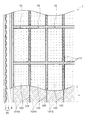
有機EL表示装置の構成は図7の従来構成を示す部分断面図に示す通りである。すなわち複数の有機EL素子10は、それぞれ例えば白色の光を発光可能な発光層102を、ホール注入電極(「陽極」または「アノード」とも称する)101と電子注入電極(「陰極」または「カソード」とも称する)11で挟んだ構成を有する。トップエミッション(TE)型と呼ばれる有機EL素子は、当図に示すように、それぞれ基板上にパターニングされた金属材料からなるホール注入電極101の上に前記発光層102を重ね、これにITO、IZO或いは薄膜金属等の透明電極、或いは半透明電極で構成した電子注入電極11を積層した構成を有する。これにより、駆動時において発光層102からの発光が基板に遮られることなく、当該電極注入電極11が配された側を前面として取り出せる特徴を持つ。前記金属材料からなる前記ホール注入電極は、発光層102における発光を前面に反射させ、発光効率を向上させる役目もなす。
The configuration of the organic EL display device is as shown in the partial sectional view of the conventional configuration in FIG. That is, each of the plurality of
なお、上記構成のように各有機EL素子10がすべて同色(白色)発光をなす構成の場合は、それぞれ複数の有機EL素子に跨って設けることが可能である。この際、発光層102及び電子注入電極11は蒸着法等によって配設できる。
前記基板には、例えばアクティブマトリクス型TFT基板30等が利用される。前記発光層102は、例えば青色発光層とオレンジ色発光層を積層することで構成できる。そして、各有機EL素子10の配置位置に合わせ、三原色のカラーフィルター61R、61G、61Bのいずれか或いは色変換層(不図示)を積層した透明基板を対向させて設けることで、基板全体でマルチカラー或いはフルカラーで画像表示がなされる。カラーフィルターを用いる方法は、各発光層102に蛍光体材料を混入したり、素子の塗り分け操作などが不要であるほか、プロセスが簡単化されるのでコスト削減および高精細ディスプレイとしても好適な技術である。
In the case where each
As the substrate, for example, an active
カラーフィルター61R、61G、61Bの間隙には視認性を改善するためのブラックマトリクスBMが配設されることがある。
なお一般には、色毎に対応するカラーフィルター61R、61G、61Bの厚みが異なるため、全体的に前記厚みの凹凸をなくす目的で、例えば特許文献1のごとく、カラーフィルター61R、61G、61Bをアクリル系樹脂、エポキシ系樹脂等からなる平坦膜60でオーバーコートするようになっている。
A black matrix BM for improving visibility may be disposed in the gaps between the
Generally, the
ここで、有機EL素子10中の発光層102は水分に弱いという性質を持つ。このため発光層102が水に触れると変質してしまい、発光強度の低下や寿命劣化など、表示性能に悪影響を及ぼす恐れがある。したがって有機EL表示装置では、外界の水分からできるだけ発光層102を隔離する必要がある。
しかしながら、上記構成を有する有機EL表示装置では、次のような問題が存在する。
第一に、現在の有機EL表示装置では、非点灯領域(いわゆるダークスポット)の発生をなくす程度に発光層102の防湿対策が十分図られているとは言い難い。その原因を本願発明者が鋭意検討したところ、発光層102までの水分の主な浸入経路としては、TFT基板30と接着層5の界面の他、平坦膜60と接着層5の界面が考えられる。
However, the organic EL display device having the above configuration has the following problems.
First, in the current organic EL display device, it is difficult to say that the moisture-proof measures of the light-emitting
このうち図7の従来図に示すように、平坦膜60と接着層5の界面(L5+L6)は、特に注意すべき箇所である。当該界面に水分が浸入すると、水分はディスプレイ全体にわたり広く拡散してしまい、非点灯領域(いわゆるダークスポット)の発生を招き、著しく表示性能を低下させる原因となる。
さらに第二に、現在の有機EL表示装置ではディスプレイの視認性に関する問題が挙げられる。現在のディスプレイでは、視野角が増すにつれて隣接素子同士での混色が発生することがあり、望みの色再現が良好になされない場合がある。このような視認性の問題は、特にフルカラー表示をなす構成の場合には特に解決すべき課題となる。
Among these, as shown in the conventional diagram of FIG. 7, the interface (L5 + L6) between the
Secondly, the current organic EL display device has a problem related to the visibility of the display. In current displays, as the viewing angle increases, color mixing between adjacent elements may occur, and desired color reproduction may not be achieved. Such a visibility problem is a problem to be solved particularly in the case of a configuration for full color display.
本発明は以上の課題に鑑みて為されたものであって、第一の目的は、特にカラーフィルターが配された透明基板付近において高い防湿性を発揮することで、良好な表示性能の実現が可能な有機EL表示装置を提供することにある。また第二の目的は、従来に比べて色再現の良い有機EL表示装置を提供することにある。 The present invention has been made in view of the above problems, and the first object is to realize high display performance by exhibiting high moisture resistance particularly in the vicinity of a transparent substrate on which a color filter is arranged. The object is to provide a possible organic EL display device. A second object is to provide an organic EL display device having better color reproduction than conventional ones.
上記課題を解決するために、本発明は、TFT基板表面に複数の有機発光素子が配設されてなるバックパネルが、フロントパネルと対向配置されてなる有機発光表示装置であって、前記フロントパネルは、透明基板表面に複数箇所にわたり、前記TFT基板上の有機発光素子に対向するようにカラーフィルター或いは色変換層が積層されてなり、フロントパネルとバックパネルの間には、前記カラーフィルター或いは色変換層を直接被覆するように、両パネルを接着する単一の接着層が配設されているものとした。 In order to solve the above problems, the present invention provides an organic light emitting display device in which a back panel in which a plurality of organic light emitting elements are disposed on a surface of a TFT substrate is disposed opposite to a front panel. Is formed by laminating a color filter or a color conversion layer so as to face the organic light emitting element on the TFT substrate over a plurality of locations on the surface of the transparent substrate, and between the front panel and the back panel, the color filter or color A single adhesive layer for adhering both panels was provided so as to directly cover the conversion layer.
ここで、前記複数の有機発光素子はTFT基板表面においてマトリクス状に配設され、当該マトリクスの行列いずれかの方向に沿って、異なる色表示をなすように、各表示色に対応したカラーフィルターが配設されたものとすることができる。
さらに前記複数の有機発光素子はマトリクスの行列いずれかの方向に沿って、三原色に対応するように繰り返し配列されており、カラーフィルターは、前記三原色に対応する素子ごと、或いは同色表示をなす行列いずれかの方向で隣接する素子グループに対応して設けられているものとした。
Here, the plurality of organic light emitting elements are arranged in a matrix on the surface of the TFT substrate, and color filters corresponding to the display colors are provided so as to display different colors along any direction of the matrix. It can be arranged.
Further, the plurality of organic light emitting elements are repeatedly arranged so as to correspond to the three primary colors along any direction of the matrix of the matrix, and the color filter is provided for each element corresponding to the three primary colors or a matrix that displays the same color. It is assumed that they are provided corresponding to element groups adjacent to each other in that direction.
また本発明は、前記複数の有機発光素子のマトリクス周囲を囲繞するように、TFT基板と透明基板の間において、前記接着層材料と異なる材料からなる封止部材が配設されているものとした。
また本発明は、前記透明基板に形成されたカラーフィルター或いはこれに加えて色変換層には、さらに積層厚みを調整するための膜厚調整層が積層することができる。
In the present invention, a sealing member made of a material different from the adhesive layer material is disposed between the TFT substrate and the transparent substrate so as to surround the periphery of the matrix of the plurality of organic light emitting elements. .
In the present invention, the color filter formed on the transparent substrate or the color conversion layer in addition to the color filter can be further laminated with a film thickness adjusting layer for adjusting the laminated thickness.
さらに前記透明基板には、隣接するカラーフィルターの間隙に合わせて黒色層が形成されており、当該黒色層の厚みが、前記カラーフィルターの最大厚み以上になるように設定することができる。 Furthermore, a black layer is formed on the transparent substrate in accordance with the gap between adjacent color filters, and the thickness of the black layer can be set to be equal to or greater than the maximum thickness of the color filter.
以上のように本発明の有機発光表示装置では、フロントパネルにおいて透明基板に設けられたカラーフィルターを従来構成のように平坦化膜で被覆せず、直接単一の接着層で被覆する構成としている。
このため本発明では、フロントパネルにおいては、透明基板上に設けられたカラーフィルター、および場合によっては前記カラーフィルターに加えて色変換層や黒色層(ブラックマトリクス)の各厚みに相当する凹凸が存在するので、接着層がこの凹凸に入り込むように充填して配設することで、上記図7の従来例に比べて接着層とフロントパネルとの界面の比表面積(平面視したときの面積に対する界面の面積)が増大し、パネル平面上の一定距離に対応する前記界面に沿った距離(以降、「界面距離」と言う。)が長く設定される。この界面距離が長いほど水分がディスプレイ内部に浸入する速度が遅くできるので、本発明では前記界面を浸入経路として水分が装置内部まで浸入する速度が従来より遅延され、結果的に良好な防湿対策が発揮されることとなり、装置の長寿命化が実現される。
As described above, in the organic light emitting display device of the present invention, the color filter provided on the transparent substrate in the front panel is not covered with the flattening film as in the conventional structure, but directly covered with a single adhesive layer. .
Therefore, according to the present invention, the front panel has color filters provided on the transparent substrate, and in some cases, irregularities corresponding to the thicknesses of the color conversion layer and the black layer (black matrix) in addition to the color filter. Therefore, the specific surface area of the interface between the adhesive layer and the front panel (the interface with respect to the area in plan view) compared to the conventional example of FIG. The area along the interface corresponding to a certain distance on the panel plane (hereinafter referred to as “interface distance”) is set longer. The longer the interface distance, the slower the rate at which moisture enters the display. In the present invention, the rate at which moisture enters the device using the interface as the entry path is delayed as compared with the prior art. As a result, the service life of the device is extended.
特に、有機EL表示装置においてRGB三原色により色表示をなす場合には、各色に対応した複数のフィルターをマトリクスの行列いずれかの方向で隣接するセル毎に配設することになる。このような構成の場合、カラーフィルターの配設数に比例して、前記界面距離が長く確保され、本発明の防湿効果を良好に得ることができる。
なお、本発明の接着層を単一のものとしたのは、複数の接着層を例えば積層構造として用いた場合、異なる接着層同士の間に新たな界面が発生し、水分浸入経路となる可能性があるため、これを排除する目的で設定したものである。
In particular, when color display is performed with the three primary colors of RGB in the organic EL display device, a plurality of filters corresponding to the respective colors are arranged for each adjacent cell in either direction of the matrix of the matrix. In such a configuration, the interfacial distance is ensured to be long in proportion to the number of arranged color filters, and the moisture-proof effect of the present invention can be obtained satisfactorily.
Note that the single adhesive layer of the present invention is used when a plurality of adhesive layers are used as a laminated structure, for example, a new interface is generated between different adhesive layers, which may be a moisture intrusion route. Therefore, it is set to eliminate this.
また、本発明は三原色やフルカラー表示に限らず、前記透明基板の表面で複数箇所にわたりカラーフィルターを配設すればよいので、例えば単色表示をなす構成の場合であっても同様の効果が期待できる。
さらに本発明では、カラーフィルター等に膜厚変換層を積層することで、さらに前記界面の表面積を増大させ、水分の浸入を遅延して効果的な防湿対策を図ることができる。
In addition, the present invention is not limited to the three primary colors and full color display, and it is only necessary to dispose color filters over a plurality of locations on the surface of the transparent substrate. Therefore, for example, the same effect can be expected even in the case of a configuration that performs a single color display. .
Furthermore, in the present invention, by laminating a film thickness conversion layer on a color filter or the like, it is possible to further increase the surface area of the interface, delay the intrusion of moisture, and take an effective countermeasure against moisture.
また本発明では、カラーフィルターよりも膜厚が厚くなるようにブラックマトリクスを配設することによっても、フロントパネルの表面積を増大させて上記防湿効果を得ることができる。一方、厚膜に形成されたブラックマトリクスによって隣接素子同士を確実に区画することで、視野角が増大しても混色の発生を防ぎ、優れた表示性能を発揮することが可能になっている。 In the present invention, the moisture-proof effect can also be obtained by increasing the surface area of the front panel by disposing the black matrix so that the film thickness is larger than that of the color filter. On the other hand, by reliably partitioning adjacent elements with a black matrix formed in a thick film, it is possible to prevent the occurrence of color mixing even when the viewing angle increases and to exhibit excellent display performance.
(実施の形態1)
1-1.TFT型有機EL表示装置の全体構成
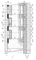
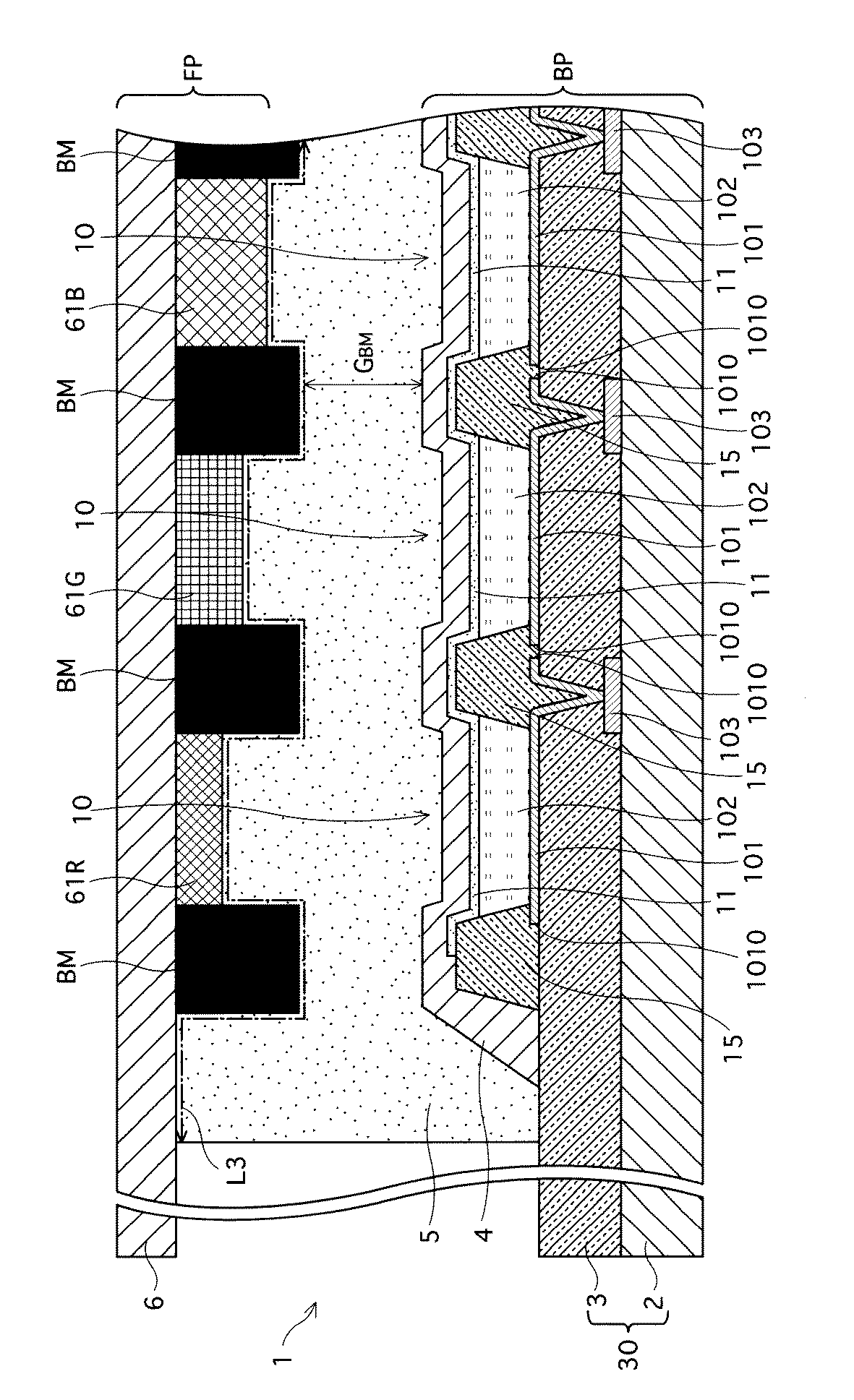
図1は、本発明の実施の形態1におけるTFT型有機EL表示装置の部分的な構成を示す上面図である。また、図2は当該有機EL表示装置の部分的な断面図である。
まず図1および図2に示すように、本有機EL表示装置1は、フロントパネルFPとバックパネルBP、および両基板FP、BPの間に配設した接着層5等で構成されており、フロントパネルFP(図1では紙面上方)側から発光を取り出すトップエミッション構造としている。
(Embodiment 1)
1-1. Overall Configuration of TFT Organic EL Display Device FIG. 1 is a top view showing a partial configuration of a TFT organic EL display device according to
First, as shown in FIGS. 1 and 2, the organic
バックパネルBPは、TFT基板30と、複数の有機EL素子10、セル分離膜15、保護膜4等で構成される。
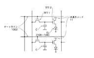
TFT基板30はLCD(液晶ディスプレイ)にも利用される多結晶シリコン等からなる能動層を有するTFTを備えた公知のものであって、ガラス等の無機材料からなるメイン基板2に、例えば図3の回路図に示すように所定の配線パターンで電源ライン103、共通ゲートライン1002、コンデンサC、TFT1、2等が形成されている。このうちコンデンサC、TFT1、2は、各有機EL素子10に対応する位置ごとにそれぞれ設けられる。共通ゲートライン1002、電源ライン103、および後述する共通カソード11等には、それぞれ公知のラインドライバが接続されており、外部より入力される映像信号に基づいた所定のパルスが印加されるようになっている。
The back panel BP includes a
The
このTFT基板30のメイン基板2の表面に、前記配線パターンを埋設するように、絶縁性材料からなる平坦化膜3が形成される。当該平坦化膜3は、当該膜上に載置されるデバイスに対して平坦性を呈することで、位置決め時や接合時などに安定性を発揮する役割をなす。このような平坦化膜3には部分的に間隙があり、当該間隙に合わせて前記配線パターンを露出する領域が設けられ、これによって図2に示すように、前記配線パターンとの各種接続、例えば各有機EL素子10のアノード101と電源ライン103との接続、或いはTFT2と共通カソード11との接続がなされるようになっている。
A
各有機EL素子10は、TFT基板30側から、第一電極としてアノード(ホール注入電極)101、発光層102、第二電極として共通カソード11(電子注入電極)がそれぞれ同順に積層された構成からなる。
アノード101は、例えばMo、Cr等金属材料を厚さ100nm程度に加工したものであって、図1中のX線に沿った素子下層領域に示すように、列方向を長手方向として、行方向に複数にわたりストライプ状に併設されている。これによりアノード101のいずれかは、列方向に並ぶ1ラインごとの複数の有機EL素子10に対して共通電極となっている。
Each
The
共通カソード11はITO、IZO等の透明電極材料を厚み10nm〜20nmの範囲で加工して構成されており、全ての有機EL素子10に対して全面的に配設されている(図2を参照)。図1では内部説明のため、共通カソード11の図示を省略している。
発光層102は、例えば青色発光する発光層と、青色と補色の関係にあるオレンジ色で発光する発光層とを積層させて白色発光をなすように構成される。なお、図1、2には図示していないが、より詳細には、発光層102の下にはTFT基板30側から、厚み100nmのトリフェニルアミン誘導体からなるホール注入層、厚さ20nmのジアミン誘導体からなるホール輸送層が順次積層されている。このような発光層102の構成例では、5〜10Vの駆動電圧を印加することにより1000〜3000cd/m2程度の輝度を発揮することができる。
The
The
なお本発明では、上記図1および図2のように、各有機EL素子10がすべて同色(白色)発光をなす構成の場合は、複数の有機EL素子10に跨って、蒸着法等により、発光層102及び共通カソード11(電子注入電極)を設けることが可能である。
また、駆動時の発光表示色は、後述のカラーフィルター61R、61G、61Bを配設することによって調整される。
In the present invention, as shown in FIG. 1 and FIG. 2, when all the
Further, the light emission display color at the time of driving is adjusted by disposing
さらにTFT基板30では、前記構成を持つ有機EL素子10をそれぞれ挟むように、各素子10を分離区画するための格子状のセル分離膜15が形成されている。当該セル分離膜15は、絶縁性材料を台形断面形状で構成され、図2に示すように、前記有機EL素子10の下より露出する各アノード101のエッジ部1010を被覆するように形成されている。これはエッジ部1010における形状がフォトエッチング等の加工処理によって作製されることで比較的鋭利になっているため、部分的に異極性部分と接触してショートを発生しないように、これを被覆して保護する目的でなされたものである。また、隣り合う有機EL素子10間で混色を生じる問題を防ぐ目的でも配設する。
Further, on the
保護膜4は、絶縁性材料(可視域における透明性が高く、電気絶縁性を有し、水分、酸素等に対するバリア性を有する材料、例えば、SiOx、SiNx、AlOx等)を、スパッタ法、蒸着法、CVD法などで成膜して構成されており、前記マトリクス配列をなす有機EL素子10とセル分離膜15をともに被覆し封止するように配される。当該保護膜4は、有機EL素子10を包含することで皮膜保護の役目を果たし、さらに装置外部より水分が浸入し、発光層102が変質するのを防ぐ等の目的で設けられる。
The
接着層5は、可視光透過率を有し、1.3〜2.5の屈折率とを有する材料、例えば、透明シリコーンゴム、透明シリコーンゲル、エポキシ樹脂、アクリル樹脂のような有機材料などを利用した透明性に優れる材料からなり、接着層5全体として単一の構成となっている。そして、バックパネルBPに対しては前記保護膜4の上からTFT基板30の片主面を被覆するように設けられ、フロントパネルFPには透明基板6の表面からカラーフィルター61R、61G、61BおよびブラックマトリクスBMを直接被覆するように設けられる。当該接着層5は、前記保護膜4とともに、発光層102を外界の水分より隔離して維持する役目もなす。
The
接着層5の形成方法としては、フロントパネルFPとバックパネルBPを対向配置させた後、減圧条件下で両パネルFP、BP間に充填する方法の他、厚膜形成法などの印刷法を利用して両パネル表面、或いはどちらか一方のパネル表面にそれぞれ塗布し、減圧下で貼り合わせて形成する方法も挙げられる。
なお、本発明における「接着層5」は、単一構成からなるものであって、例えば複数の異なる材料からなる積層構造の接着層は含まれない。さらに、従来フロントパネルFP表面に被覆するように形成されていた「平坦膜」など、材料の異なるものも含まないものとする。これは、接着層5自体の内部で異なる材料が存在することで、水分浸入経路となりうる界面が形成されるのを防ぐ理由による。
As a method for forming the
The “
一方、フロントパネルFPは、透明基板6、カラーフィルター61R、61G、61B、ブラックマトリクスBM等で構成される。
透明基板6は、例えば透明性の高いソーダライムガラス材料や無アルカリガラス材料から構成することができる。
カラーフィルター61R、61G、61Bは、前記透明基板6の表面において、バックパネルBPに設けられた有機EL素子10の各位置に対応するように、セル分離膜15の間隙位置に合わせて個別に設けられる。本実施の形態1では、カラーフィルター61R、61G、61Bは前記マトリクスの列方向に沿って帯状に形成されており、当該列方向に配列する白色の有機EL素子10のグループで共有する構成となっている。
On the other hand, the front panel FP includes a
The
The
なお、カラーフィルター61R、61G、61Bの配設の仕方としては、この他に、セル毎に一つずつ設けるようにしてもよい。
さらに、図2では示していないが、当該カラーフィルター61R、61G、61Bの上下いずれかに色変換層を積層して設ける場合もあるし、或いは色変換層を単独で用いる場合もある。当該色変換層は、駆動時の発光色を調整するためのものである。
In addition, as a method of arranging the
Furthermore, although not shown in FIG. 2, a color conversion layer may be provided by being laminated on the upper or lower side of the
ブラックマトリクスBMはいわゆる黒色層であって、カラーフィルター61R、61G、61Bの間隙に合わせ、ディスプレイ正面から見て各有機EL素子10の周囲を囲むように設けられる。なお、この構成例ではブラックマトリクスBMはカラーフィルター61R、61G、61Bよりも薄膜で形成されている。
以上の構成を有する有機EL表示装置1によれば、駆動時には図3の回路図に示すように、まず個別の電源ライン103のいずれか及び共通ゲートライン1002に対して給電がなされると、TFT1においてスイッチングが行われ、これに接続されたコンデンサCへデータが書き込まれる。その後は、電源ライン103を介してアノード101と共通カソード11に給電することにより、前記データが書き込まれたコンデンサCの位置に対応する有機EL素子10において発光がなされる。このとき、データが書き込まれた前記コンデンサCからの出力は、当該コンデンサCに接続されたTFT2を介して任意の有機EL素子10側に送られるようになっているので、TFT2において出力調整を行うことで素子の発光強度の調整がなされることとなる。
The black matrix BM is a so-called black layer, and is provided so as to surround the periphery of each
According to the organic
1-2.本実施の形態の特徴について
本実施の形態1特徴は、フロントパネルFPの透明基板6の表面において、カラーフィルター61R、61G、61Bのそれぞれが接着層5に対して直接接触するように配設されている点にある。表示装置1ではこのような工夫を行うことによって、接着層5と対向するフロントパネルFPの表面積を広く確保し、装置外部からフロントパネルFPと接着層5との接触界面を経路とする水の浸入を遅延させ、結果として比較的長期にわたり高い防湿性が発揮されるように図られている。
1-2. Features of the present embodiment The feature of the first embodiment is that the
具体的には、各色に対応するカラーフィルター61R、61G、61BとブラックマトリクスBMを配設した透明基板6の表面は、従来ではこれらをオーバーコートするようにフラットな表面を持つ平坦膜60が形成されていたので(図7を参照)、接着層5と平坦膜60の界面がフラットである。したがって、この界面を浸入経路(L5+L6)として装置外部より水分が浸入すると、比較的速い時期にディスプレイの中央部まで浸透し、前記界面からバックパネルBPとのギャップGR、GB、GGを介してバックパネルBPの発光層102に水分が混入してダークスポット(不点灯領域)を形成することがあった。これに対し、本実施の形態1では各カラーフィルター61R、61G、61BとブラックマトリクスBMの層厚みの差分によって形成される壁面の面積だけフロントパネルFPの表面積が増大しているので、例え前記界面を浸入経路として水分が浸入したとしても水分の浸入速度が遅延される。発光層102は本来水に弱いという化学的性質を有しているが、本実施の形態1では上記水分浸入の遅延効果によって、高い防湿性のもとに発光層102の変質が抑制され、ダークスポットの多発を防止して、比較的長期にわたり安定した発光性能および表示性能が実現されることとなる。
Specifically, on the surface of the
なお、本発明はこのようにフロントパネルFPの表面積が平坦膜を用いる従来構成のものより増大させる点に特徴があるが、カラーフィルター61R、61G、61BとブラックマトリクスBMのパターン形状、積層厚み等の設定は従来と同様であっても、平坦膜60を形成しなければフロントパネルFPの表面積は増大する。しかしながら上記図2の構成ならびに他の実施の形態でも説明するように、カラーフィルター61R、61G、61BとブラックマトリクスBMの少なくともいずれかの厚みを増大させ、結果としてフロントパネルFPの表面積をさらに増大させるようにすれば、水分浸入の速度をより遅延させることができるので望ましい。また、カラーフィルター61R、61G、61BとブラックマトリクスBMの膜厚が同じでも、平坦膜60を用いなければフロントパネルFPの表面積は多少増大する。
Note that the present invention is characterized in that the surface area of the front panel FP is increased as compared with the conventional configuration using a flat film, but the pattern shape of the
以下、その他の実施の形態について、実施の形態1との差違を中心に説明する。
(実施の形態2)
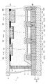
図4は、本発明の実施の形態2における有機EL表示装置の構成を示す装置断面図である。
実施の形態1との違いは、色の異なるカラーフィルターにおいて厚みのばらつきがある場合、その厚みの薄いカラーフィルター(ここでは61Rと62G)に厚膜調整層62R、62Gを積層し、全てのカラーフィルターの見かけ上の厚みが同様になるように調整した点にある。膜厚調整層62R、62Gは透明性に優れる材料から構成される。
Hereinafter, other embodiments will be described focusing on differences from the first embodiment.
(Embodiment 2)
FIG. 4 is a device cross-sectional view showing the configuration of the organic EL display device according to
The difference from the first embodiment is that when there are variations in thickness among color filters of different colors, the thick film adjustment layers 62R and 62G are laminated on the thin color filters (61R and 62G here), and all the colors The filter is adjusted to have the same apparent thickness. The film
このような構成によっても、上記実施の形態1と同様の効果が奏される。特に、膜厚調整層62R、62Gを設けたことによって、フロントパネルFP表面の凹凸がさらに大きくなり、その表面積も増大するので、接着層5との界面L2を伝って装置外部より水分が浸入した場合は、その浸入速度が実施の形態1よりも効果的に遅延され、長期にわたって安定した駆動が可能となる。
Even with such a configuration, the same effects as those of the first embodiment can be obtained. In particular, by providing the film
また、本実施の形態2では、、膜厚調整層62R、62Gを設けたことによって、各カラーフィルター61R、61G、61BとバックパネルBPとのギャップGR、GG、GBを一定距離に調整されるため、RGB各色の視野角依存性を揃えることができ、優れた発光色特性も発揮されるというメリットもある。
(実施の形態3)
図5は、本発明の実施の形態3における有機EL表示装置の構成を示す装置断面図である。
In the second embodiment, by providing the film
(Embodiment 3)
FIG. 5 is a device cross-sectional view showing a configuration of an organic EL display device according to
本実施の形態3の構成は、基本的には実施の形態1と同様であるが、ブラックマトリクスBMの厚みをカラーフィルター61R、61G、61Bの最大厚み(ここでは61B)よりも厚くなるように設定した点にある。
このような構成によれば、ブラックマトリクスBMが膜厚になった分、フロントパネルFPの表面積が増大するので、実施の形態1と同様の効果がさらに有効に発揮され、高い防湿効果のもとに品質の信頼性が確保される。特に本実施の形態1では、ブラックマトリクスBMが透明基板6表面より大きく突出しているため、接着層5との界面L3に外部より浸入した水分はこのブラックマトリクスBMの障壁によって有効に遮断される。したがって、前記水分はブラックマトリクスBMとバックパネルBPとのギャップGBMを伝い、バックパネルBP側へ浸入するのが困難となっている。
The configuration of the third embodiment is basically the same as that of the first embodiment, but the thickness of the black matrix BM is larger than the maximum thickness of the
According to such a configuration, since the surface area of the front panel FP is increased by the amount of the black matrix BM, the same effect as that of the first embodiment is more effectively exhibited, and the high moisture-proof effect is obtained. Quality reliability is ensured. In particular, in the first embodiment, since the black matrix BM protrudes larger than the surface of the
また、本実施の形態3では各カラーフィルター61R、61G、61Bが厚膜のブラックマトリクスBMによって囲繞された構成となっているため、広い視野角にわたり隣接する異なる色間での混色が防止され、良好な発光色特性を発揮することも可能である。
なお、本実施の形態3では、ブラックマトリクスBMの厚みをカラーフィルター61R、61G、61Bの最大厚みよりも厚くする例について説明したが、ブラックマトリクスBMの厚みは必ずしもカラーフィルター61R、61G、61Bの最大厚みより厚くする必要はなく、若干薄く形成してもそれなりの効果は望める。
In the third embodiment, the
In the third embodiment, the example in which the thickness of the black matrix BM is made larger than the maximum thickness of the
(実施の形態4)
図6は、本発明の実施の形態4における有機EL表示装置の構成を示す装置断面図である。
本実施の形態4は、内部構造は実施の形態1と同様であるが、これに加えてパネル周縁(最外周)の接着層5の側面に対し、これを囲繞するように防湿材料からなる封止部材として防湿壁7を設けた点に特徴を有する。
(Embodiment 4)
FIG. 6 is a device cross-sectional view showing a configuration of an organic EL display device according to
In the fourth embodiment, the internal structure is the same as that of the first embodiment, but in addition to this, the side wall of the
防湿壁7の材料としては、例えば可視光硬化型接着剤、熱硬化型接着剤、もしくは紫外線硬化型接着剤の他、PTFEなど撥水性を持つフッ素化合物からなる材料を用いることで、さらに防湿性を高めるようにしてもよい。
このような構成を持つ本実施の形態4によれば、実施の形態1よりもさらに水分浸入を抑制させることが可能である。特に、図6に示す本実施の形態4では、透明基板6とTFT基板30とのギャップに嵌り込むように防湿壁7を設けているので、フロントパネルFPと接着層5の界面L4に加え、接着層5とTFT基板30との界面に対しても防湿効果が発揮される。このため、より安定した駆動と長期安定性が実現されるようになっている。
As a material for the moisture barrier 7, for example, in addition to a visible light curable adhesive, a thermosetting adhesive, or an ultraviolet curable adhesive, a material made of a fluorine compound having water repellency, such as PTFE, is used to further improve moisture resistance. You may make it raise.
According to the fourth embodiment having such a configuration, it is possible to further suppress moisture intrusion than in the first embodiment. In particular, in
なお、防湿壁7は、パネル周囲を完全に囲繞する必要はなく、一部領域に設けてもある程度の効果は期待できる。
(実施例)
ここでは本発明の効果を確認すべく、実施例と比較例の有機EL表示装置をそれぞれ作製し、駆動させて性能評価を行った。
The moisture barrier 7 does not need to completely surround the periphery of the panel, and a certain effect can be expected even if it is provided in a partial region.
(Example)
Here, in order to confirm the effect of the present invention, organic EL display devices of Examples and Comparative Examples were respectively produced and driven to perform performance evaluation.
<測定実験1>
上記実施の形態1〜4の有機EL表示装置をそれぞれ実施例1〜4として作製した。また、図7に示す構成を比較例1とし、これに実施の形態4と同様の防湿壁7を設けた構成を比較例2としてそれぞれ作製した。
実験項目は高温耐湿実験(85℃/85%RH、経過時間 の条件)と、ディスプレイの視野角依存性における測定である。
<
The organic EL display devices of
The experimental items are high temperature and humidity resistance experiments (85 ° C / 85% RH, elapsed time conditions) and measurements on the viewing angle dependence of the display.
実験結果を以下の表1に示す。なお、記載した数値は比較例1のデータを基準とした場合の相対値である。
The experimental results are shown in Table 1 below. The numerical values described are relative values based on the data of Comparative Example 1.
次に、上記実施の形態1の有機EL表示装置について、カラーフィルタの膜厚と水分浸入速度について調査実験を行った。カラーフィルタの膜厚は、当該実験では実際の有機EL表示装置に形成されるフィルタ膜厚に相当する0.5μm〜20μmの範囲で変化させ、実施例5〜14を作製した。
Next, with respect to the organic EL display device of the first embodiment, an investigation experiment was conducted on the film thickness of the color filter and the moisture intrusion rate. In this experiment, Examples 5 to 14 were prepared by changing the thickness of the color filter in the range of 0.5 to 20 μm corresponding to the filter thickness formed in the actual organic EL display device.
また、フロントパネルFPに平坦膜をオーバーコートし、これを分離膜を備えないアクティブマトリクス型のバックパネルBPと組み合わせた有機EL表示装置を比較例3として作製した。
さらに、フロントパネルFPに平坦膜をオーバーコートし、これをTFT基板を用いたバックパネルBPと組み合わせた有機EL表示装置を比較例4として作製した。
Further, an organic EL display device in which a flat film was overcoated on the front panel FP and this was combined with an active matrix back panel BP having no separation film was produced as Comparative Example 3.
Further, an organic EL display device in which a flat film was overcoated on the front panel FP and combined with a back panel BP using a TFT substrate was produced as Comparative Example 4.
パネルサイズは2.4インチQVGA規格(320×240×RGB)とし、表示部のサイズは3.6cm×4.8cm(対角6.0cm)とした。使用するTFT基板の表面には、各有機EL素子が構成するセル毎に厚み1.0μmの平坦化膜があるものを使用した。ここでは前記TFT基板の平坦化膜が矩形状断面を持つものと仮定して計算を行った。
実験結果を以下の表2に示す。
The panel size was 2.4 inch QVGA standard (320 × 240 × RGB), and the size of the display unit was 3.6 cm × 4.8 cm (diagonal 6.0 cm). On the surface of the TFT substrate to be used, one having a planarizing film with a thickness of 1.0 μm for each cell constituting each organic EL element was used. Here, the calculation was performed on the assumption that the planarizing film of the TFT substrate has a rectangular cross section.
The experimental results are shown in Table 2 below.
なお、R-CF、G-CF、B-CFはそれぞれ赤、緑、青の各カラーフィルタを示す。
また表2中の「距離比(TFT/CF)」とは、パネル横方向に沿った断面において、TFT基板表面に沿った長さ(TFT)、およびフロントパネルFPの界面に沿った長さ(CF)の比を表したものである。
また、表2中の「発光中心までの距離」とは、パネル横方向端部から前記フロントパネルFPと接着層の界面に沿って、中央部に達するまでの距離を表す。
R-CF, G-CF, and B-CF represent red, green, and blue color filters, respectively.
The “distance ratio (TFT / CF)” in Table 2 is the length along the TFT substrate surface (TFT) and the length along the interface of the front panel FP (in the cross section along the horizontal direction of the panel). CF) ratio.
The “distance to the light emission center” in Table 2 represents the distance from the lateral end of the panel to the center along the interface between the front panel FP and the adhesive layer.
さらに表2中の「水蒸気の到達時間」とは、前記パネルの中央部に水蒸気が達するまでの時間を表す。また実施例12以降のかっこ内の数値は、実施例5〜11の時間との差分を表す。
Furthermore, “water vapor arrival time” in Table 2 represents the time until water vapor reaches the center of the panel. Moreover, the numerical value in the parenthesis after Example 12 represents the difference with the time of Examples 5-11.
まず表1に示すデータから、耐湿性において、本発明の実施例1〜4の有機EL表示装置のいずれもが、従来構成の比較例1および2の有機EL表示装置より優れた特性を持つことが明らかになった。高温高湿実験を行った結果、本発明の有機EL表示装置では水分の浸入が効果的に抑制され、高い耐性が発揮されたものと推測される。
First, from the data shown in Table 1, in terms of moisture resistance, all of the organic EL display devices of Examples 1 to 4 of the present invention have characteristics superior to those of the organic EL display devices of Comparative Examples 1 and 2 having the conventional configuration. Became clear. As a result of conducting a high temperature and high humidity experiment, it is presumed that in the organic EL display device of the present invention, intrusion of moisture is effectively suppressed and high tolerance is exhibited.
一方、比較例2のデータからは、従来構成に対して単にパネル周囲に防湿壁を設けても、それほど耐湿性は向上しないことが分かった。したがって、効果的な防湿対策を行うためには、基本的に本発明において、少なくとも実施例1のようにフロントパネルFPの表面積を増大させることが必要であって、こうすることで例えフロントパネルFPと接着層5の界面端部に水分が浸入したとしても、その浸入速度が遅延されるので、パネル全体にわたり安定した駆動が期待できる。
On the other hand, from the data of Comparative Example 2, it was found that the moisture resistance is not improved so much even if a moisture barrier is simply provided around the panel as compared with the conventional configuration. Therefore, in order to take effective moisture-proof measures, basically, in the present invention, it is necessary to increase the surface area of the front panel FP at least as in the first embodiment. Even if moisture enters the interface end portion of the
また視野角についての性能も、実施例1〜4では従来の比較例1および2に劣らない性能を有していることが分かった。特に実施例3ではブラックマトリクスをカラーフィルターより厚膜になるように形成しているため、混色などの問題の発生が防止されることで、高い表示性能が発揮されることが分かった。このように本発明は、有機EL表示装置の表示性能の向上対策としても有効なものである。 Moreover, it turned out that the performance about a viewing angle has the performance which is inferior to the conventional comparative examples 1 and 2 in Examples 1-4. In particular, in Example 3, since the black matrix is formed to be thicker than the color filter, it has been found that high display performance is exhibited by preventing the occurrence of problems such as color mixing. Thus, the present invention is also effective as a measure for improving the display performance of the organic EL display device.
次に表2のデータからは、実施例12〜14のように、カラーフィルターの厚みが0.5μm〜1μmの小さい値の範囲であっても、結果的に「発光中心までの距離」に示すように、フロントパネルFPの表面積が増大するので、比較例3または4に比べて防湿効果が高くなっている。
なお実施例では、カラーフィルターの厚みが増すにつれて防湿効果は高まるが、当該実験では実施例5〜11のデータに示すように、各カラーフィルターの厚みが全て1.0μmを超え、分離膜の厚みを超えると、有機EL表示装置の防湿効果はTFT基板と接着層との間の浸入経路における防湿効果に依存するようになり、見かけ上の本発明の効果による水分浸入速度は一定となる。このため、より高い防湿効果を得るためには、例えば実施の形態4(実施例4)に示すように、TFT基板付近からの防湿効果も合わせて得られるように防湿壁を設ける等の工夫を行う必要がある。実施の形態4の構成は、実施の形態1の構成を基本とし、パネル周囲を防湿材料で囲繞するだけで実現できるので、比較的簡単な構成で高い防湿効果が期待できるため好適である。
Next, from the data of Table 2, as shown in Examples 12 to 14, even when the thickness of the color filter is in a small value range of 0.5 μm to 1 μm, the result is shown as “distance to the emission center”. As described above, since the surface area of the front panel FP is increased, the moisture-proof effect is higher than that of Comparative Example 3 or 4.
In the examples, the moisture-proof effect increases as the thickness of the color filter increases. However, in the experiment, as shown in the data of Examples 5 to 11, all the thicknesses of the color filters exceed 1.0 μm, and the thickness of the separation membrane. Exceeding the above, the moisture-proof effect of the organic EL display device depends on the moisture-proof effect in the penetration path between the TFT substrate and the adhesive layer, and the moisture penetration rate due to the apparent effect of the present invention becomes constant. For this reason, in order to obtain a higher moisture-proof effect, for example, as shown in Embodiment 4 (Example 4), a device such as providing a moisture-proof wall so as to obtain a moisture-proof effect from the vicinity of the TFT substrate is also provided. There is a need to do. The configuration of the fourth embodiment is based on the configuration of the first embodiment, and can be realized simply by surrounding the panel with a moisture-proof material. Therefore, a high moisture-proof effect can be expected with a relatively simple configuration, which is preferable.
表2に示す実施例のデータから、次の関係が成立する。
すなわち、透明基板表面に積層したカラーフィルターの厚みが0.5μm以上20μm以下の範囲であるとともに、前記TFT基板に形成された平坦膜の厚みが0.5μm以上2.0μm以下の範囲であって、前記有機発光表示装置の一断面部分におけるフロントパネルと接着層との界面長さをa、当該一断面部分におけるバックパネルと接着層との界面長さをbとするとき、
0.57≦b/a≦1.02
の関係が存在するように設定することが高い防湿効果を得るために望ましいと考えられる。b/aが1.02より大きい場合、もしくはb/aが0.57未満である場合のいずれでも、好ましい効果は得られにくい。しかしながら、この数値範囲はカラーフィルターおよびTFT基板の平坦膜の厚みに依存するものであって、これらのサイズが変われば最適範囲も変化する。
From the data of the example shown in Table 2, the following relationship is established.
That is, the thickness of the color filter laminated on the transparent substrate surface is in the range of 0.5 μm to 20 μm, and the thickness of the flat film formed on the TFT substrate is in the range of 0.5 μm to 2.0 μm. When the interface length between the front panel and the adhesive layer in one cross-sectional portion of the organic light emitting display device is a, and the interface length between the back panel and the adhesive layer in the one cross-sectional portion is b,
0.57 ≦ b / a ≦ 1.02
In order to obtain a high moisture-proof effect, it is considered desirable to set the relationship so as to exist. In any case where b / a is greater than 1.02 or b / a is less than 0.57, it is difficult to obtain a favorable effect. However, this numerical range depends on the thickness of the color filter and the flat film of the TFT substrate, and the optimum range changes as these sizes change.
本発明の有機EL表示装置は、携帯電子機器のディスプレイや、フルカラーテレビジョンなどに利用することができる。 The organic EL display device of the present invention can be used for displays of portable electronic devices, full-color televisions, and the like.
1 アクティブマトリクス型有機EL表示装置
2 メイン基板
3 平坦化膜
4 保護膜
5 接着層
6 透明基板
10 有機EL素子
11 カソード、共通カソード(電子注入電極)
15 セル分離膜
61R、61G、61B カラーフィルター
101 アノード(ホール注入電極)
102 発光層
1010 エッジ部分
DESCRIPTION OF
15
102
Claims (7)
前記フロントパネルは、透明基板表面に複数箇所にわたり、前記TFT基板上の有機発光素子に対向するようにカラーフィルター或いは色変換層が積層されてなり、
フロントパネルとバックパネルの間には、前記カラーフィルター或いは色変換層を直接被覆するように、両パネルを接着する単一の接着層が配設されている
ことを特徴とする有機発光表示装置。 A back panel in which a plurality of organic light emitting elements are disposed on the surface of the TFT substrate is an organic light emitting display device that is disposed to face the front panel,
The front panel is formed by laminating a color filter or a color conversion layer so as to face the organic light emitting element on the TFT substrate over a plurality of locations on the transparent substrate surface,
Between the front panel and the back panel, a single adhesive layer for adhering both panels is disposed so as to directly cover the color filter or the color conversion layer.
フロントパネルでは前記マトリクスの行列いずれかの方向に沿って異なる色表示をなすように、透明基板表面に表示色ごとに対応するカラーフィルターが配設されていることを特徴とする請求項1に記載の有機発光表示装置。 In the back panel, the plurality of organic light emitting elements are arranged in a matrix on the surface of the TFT substrate,
The color filter corresponding to each display color is disposed on the surface of the transparent substrate so as to display different colors along any direction of the matrix of the matrix on the front panel. Organic light-emitting display device.
カラーフィルターは透明基板表面において、前記三原色のそれぞれに対応する有機発光素子ごと、或いは同色表示をなす前記マトリクスの行列いずれかの方向に沿った有機発光素子のグループごとに対応して設けられている
ことを特徴とする請求項2に記載の有機発光表示装置。 The plurality of organic light emitting elements are repeatedly arranged on the TFT substrate surface so as to correspond to each of the three primary colors along any direction of the matrix matrix,
The color filter is provided on the transparent substrate surface for each organic light emitting element corresponding to each of the three primary colors, or for each group of organic light emitting elements along either direction of the matrix of the matrix that displays the same color. The organic light-emitting display device according to claim 2.
前記TFT基板表面上に配設された複数の有機発光素子の最外周を囲繞するように、前記接着層と異なる材料からなる封止部材が配設されていることを特徴とする請求項1〜3のいずれかに記載の有機発光表示装置。 Between the front panel and the back panel,
The sealing member which consists of a material different from the said contact bonding layer is arrange | positioned so that the outermost periphery of the some organic light emitting element arrange | positioned on the said TFT substrate surface may be enclosed. 4. The organic light emitting display device according to any one of 3 above.
当該黒色層の厚みが、前記カラーフィルターの最大厚み以上になるように設定されていることを特徴とする請求項1〜5のいずれかに記載の有機発光表示装置。 In the transparent substrate, a black layer is formed in accordance with the gap between adjacent color filters,
The organic light emitting display device according to claim 1, wherein the thickness of the black layer is set to be equal to or greater than the maximum thickness of the color filter.
前記TFT基板に形成された平坦膜の厚みが0.5μm以上2.0μm以下の範囲であって、
前記有機発光表示装置の一断面部分におけるフロントパネルと接着層との界面長さをa、当該一断面部分におけるバックパネルと接着層との界面長さをbとするとき、0.57≦b/a≦1.02
の関係が存在する
ことを特徴とする請求項1〜6のいずれかに記載の有機発光表示装置。
The thickness from the transparent substrate surface to the color filter or color conversion layer is in the range of 0.5 μm to 20 μm, and the color filter or color conversion layer is directly coated on the adhesive layer,
The flat film formed on the TFT substrate has a thickness in the range of 0.5 μm to 2.0 μm,
When the interface length between the front panel and the adhesive layer in one cross section of the organic light emitting display device is a, and the interface length between the back panel and the adhesive layer in the cross section is b, 0.57 ≦ b / a ≦ 1.02
The organic light-emitting display device according to claim 1, wherein the following relationship exists.
Priority Applications (1)
| Application Number | Priority Date | Filing Date | Title |
|---|---|---|---|
| JP2004105134A JP2005293946A (en) | 2004-03-31 | 2004-03-31 | Organic EL display device |
Applications Claiming Priority (1)
| Application Number | Priority Date | Filing Date | Title |
|---|---|---|---|
| JP2004105134A JP2005293946A (en) | 2004-03-31 | 2004-03-31 | Organic EL display device |
Publications (1)
| Publication Number | Publication Date |
|---|---|
| JP2005293946A true JP2005293946A (en) | 2005-10-20 |
Family
ID=35326666
Family Applications (1)
| Application Number | Title | Priority Date | Filing Date |
|---|---|---|---|
| JP2004105134A Withdrawn JP2005293946A (en) | 2004-03-31 | 2004-03-31 | Organic EL display device |
Country Status (1)
| Country | Link |
|---|---|
| JP (1) | JP2005293946A (en) |
Cited By (32)
| Publication number | Priority date | Publication date | Assignee | Title |
|---|---|---|---|---|
| JP2007335403A (en) * | 2006-06-14 | 2007-12-27 | Samsung Electronics Co Ltd | Display device and manufacturing method thereof |
| JP2008147161A (en) * | 2006-12-06 | 2008-06-26 | Samsung Sdi Co Ltd | Organic light emitting display |
| JP2008226747A (en) * | 2007-03-15 | 2008-09-25 | Sony Corp | Display device and electronic device |
| JP2009251560A (en) * | 2008-04-11 | 2009-10-29 | Dainippon Printing Co Ltd | Adhesive composition for laminating color filter |
| KR100953654B1 (en) * | 2008-06-26 | 2010-04-20 | 삼성모바일디스플레이주식회사 | OLED display and manufacturing method thereof |
| US7781967B2 (en) | 2006-08-30 | 2010-08-24 | Seiko Epson Corporation | Organic electroluminescence device having an improved barrier structure, and manufacturing method therefore and electronic apparatus |
| JP2010287421A (en) * | 2009-06-11 | 2010-12-24 | Toppan Printing Co Ltd | Organic EL device and manufacturing method thereof |
| JP2011040352A (en) * | 2009-08-18 | 2011-02-24 | Sony Corp | Display device |
| US7898175B2 (en) | 2007-02-06 | 2011-03-01 | Samsung Mobile Display Co., Ltd. | Organic light emitting display apparatus with an enhanced viewing angle |
| US7902751B2 (en) | 2007-11-02 | 2011-03-08 | Seiko Epson Corporation | Organic electroluminescent device, method for producing the same, and electronic apparatus |
| CN102597822A (en) * | 2010-06-16 | 2012-07-18 | 松下电器产业株式会社 | EL display panel, EL display device including EL display panel, organic EL display device, and method for manufacturing EL display panel |
| WO2013001583A1 (en) * | 2011-06-30 | 2013-01-03 | パナソニック株式会社 | Display panel and method for manufacturing display panel |
| KR20140013854A (en) * | 2012-07-27 | 2014-02-05 | 삼성디스플레이 주식회사 | Organic light emitting display device |
| WO2014049993A1 (en) * | 2012-09-26 | 2014-04-03 | Sony Corporation | Display unit and electronic apparatus |
| WO2014103708A1 (en) * | 2012-12-27 | 2014-07-03 | 大日本印刷株式会社 | Color filter forming substrate and organic el display device |
| JP2015011140A (en) * | 2013-06-28 | 2015-01-19 | 大日本印刷株式会社 | Color filter formation substrate and organic el display device |
| CN104681590A (en) * | 2013-12-02 | 2015-06-03 | 乐金显示有限公司 | Organic light emitting display device |
| JP2015103476A (en) * | 2013-11-27 | 2015-06-04 | 株式会社Joled | Display panel and manufacturing method thereof |
| KR20150069364A (en) * | 2013-12-13 | 2015-06-23 | 엘지디스플레이 주식회사 | Organic Light Emitting Diode Display Device and Method for Manufacturing The Same |
| WO2015089884A1 (en) * | 2013-12-18 | 2015-06-25 | 深圳市华星光电技术有限公司 | Wavelength selective colour filter and display structure using same |
| KR20150077292A (en) | 2013-12-27 | 2015-07-07 | 소니 주식회사 | Display unit and electronic apparatus |
| WO2016059497A1 (en) * | 2014-10-17 | 2016-04-21 | Semiconductor Energy Laboratory Co., Ltd. | Light-emitting device, module, electronic device, and method for manufacturing light-emitting device |
| CN105576003A (en) * | 2016-02-03 | 2016-05-11 | 昆山工研院新型平板显示技术中心有限公司 | Display screen body having uniform brightness |
| US20170062528A1 (en) * | 2015-08-28 | 2017-03-02 | Semiconductor Energy Laboratory Co., Ltd. | Display device |
| WO2017081575A1 (en) * | 2015-11-11 | 2017-05-18 | Semiconductor Energy Laboratory Co., Ltd. | Display device and method for manufacturing the same |
| US9917282B2 (en) | 2015-07-30 | 2018-03-13 | Semiconductor Energy Laboratory Co., Ltd. | Manufacturing method of light-emitting device, light-emitting device, module, and electronic device |
| JP2018085340A (en) * | 2011-03-02 | 2018-05-31 | 株式会社半導体エネルギー研究所 | Display device |
| CN109148718A (en) * | 2018-08-20 | 2019-01-04 | 武汉华星光电半导体显示技术有限公司 | Organic light emitting display panel and its manufacturing method |
| JP2019169480A (en) * | 2012-07-31 | 2019-10-03 | 株式会社Joled | Display unit and electronic apparatus |
| CN111430444A (en) * | 2020-04-30 | 2020-07-17 | 武汉华星光电半导体显示技术有限公司 | Quantum dot display panel and preparation method thereof |
| CN113113454A (en) * | 2021-03-26 | 2021-07-13 | 武汉华星光电半导体显示技术有限公司 | Display panel and display device |
| CN113644222A (en) * | 2021-08-13 | 2021-11-12 | 武汉天马微电子有限公司 | A display panel and display device |
-
2004
- 2004-03-31 JP JP2004105134A patent/JP2005293946A/en not_active Withdrawn
Cited By (103)
| Publication number | Priority date | Publication date | Assignee | Title |
|---|---|---|---|---|
| JP2007335403A (en) * | 2006-06-14 | 2007-12-27 | Samsung Electronics Co Ltd | Display device and manufacturing method thereof |
| US7781967B2 (en) | 2006-08-30 | 2010-08-24 | Seiko Epson Corporation | Organic electroluminescence device having an improved barrier structure, and manufacturing method therefore and electronic apparatus |
| JP2008147161A (en) * | 2006-12-06 | 2008-06-26 | Samsung Sdi Co Ltd | Organic light emitting display |
| US8022616B2 (en) | 2006-12-06 | 2011-09-20 | Samsung Mobile Display Co., Ltd. | Organic light emitting display apparatus |
| US7898175B2 (en) | 2007-02-06 | 2011-03-01 | Samsung Mobile Display Co., Ltd. | Organic light emitting display apparatus with an enhanced viewing angle |
| US8773016B2 (en) | 2007-03-15 | 2014-07-08 | Sony Corporation | Display apparatus including light emitting elements and a light shielding portion disposed on the light emitting elements and an electronic device including same |
| JP2008226747A (en) * | 2007-03-15 | 2008-09-25 | Sony Corp | Display device and electronic device |
| US8198805B2 (en) | 2007-03-15 | 2012-06-12 | Sony Corporation | Display apparatus and electronic device |
| CN102931212A (en) * | 2007-03-15 | 2013-02-13 | 索尼株式会社 | Display apparatus and electronic device |
| CN102931212B (en) * | 2007-03-15 | 2015-10-07 | 株式会社日本有机雷特显示器 | Display unit and electronic equipment |
| US7902751B2 (en) | 2007-11-02 | 2011-03-08 | Seiko Epson Corporation | Organic electroluminescent device, method for producing the same, and electronic apparatus |
| US8324805B2 (en) | 2007-11-02 | 2012-12-04 | Seiko Epson Corporation | Organic electroluminescent device, method for producing the same, and electronic apparatus |
| JP2009251560A (en) * | 2008-04-11 | 2009-10-29 | Dainippon Printing Co Ltd | Adhesive composition for laminating color filter |
| KR100953654B1 (en) * | 2008-06-26 | 2010-04-20 | 삼성모바일디스플레이주식회사 | OLED display and manufacturing method thereof |
| US8851952B2 (en) | 2008-06-26 | 2014-10-07 | Samsung Display Co., Ltd. | Method of manufacturing an organic light emitting diode display device |
| US8492969B2 (en) | 2008-06-26 | 2013-07-23 | Samsung Display Co., Ltd. | Organic light emitting diode display and method of manufacturing the same |
| JP2010287421A (en) * | 2009-06-11 | 2010-12-24 | Toppan Printing Co Ltd | Organic EL device and manufacturing method thereof |
| JP2011040352A (en) * | 2009-08-18 | 2011-02-24 | Sony Corp | Display device |
| CN102597822A (en) * | 2010-06-16 | 2012-07-18 | 松下电器产业株式会社 | EL display panel, EL display device including EL display panel, organic EL display device, and method for manufacturing EL display panel |
| CN102597822B (en) * | 2010-06-16 | 2014-09-03 | 松下电器产业株式会社 | EL display panel, EL display device including EL display panel, organic EL display device, and method for manufacturing EL display panel |
| JP2018085340A (en) * | 2011-03-02 | 2018-05-31 | 株式会社半導体エネルギー研究所 | Display device |
| KR20140030018A (en) * | 2011-06-30 | 2014-03-11 | 파나소닉 주식회사 | Display panel and method for manufacturing display panel |
| CN102959707B (en) * | 2011-06-30 | 2016-09-28 | 株式会社日本有机雷特显示器 | Display panel and method for manufacturing display panel |
| US8624481B2 (en) | 2011-06-30 | 2014-01-07 | Panasonic Corporation | Display panel and display panel manufacturing method |
| CN102959707A (en) * | 2011-06-30 | 2013-03-06 | 松下电器产业株式会社 | Display panel and method for manufacturing display panel |
| KR101689920B1 (en) | 2011-06-30 | 2016-12-26 | 가부시키가이샤 제이올레드 | Display panel and method for manufacturing display panel |
| WO2013001583A1 (en) * | 2011-06-30 | 2013-01-03 | パナソニック株式会社 | Display panel and method for manufacturing display panel |
| JPWO2013001583A1 (en) * | 2011-06-30 | 2015-02-23 | パナソニック株式会社 | Display panel and method of manufacturing display panel |
| KR20140013854A (en) * | 2012-07-27 | 2014-02-05 | 삼성디스플레이 주식회사 | Organic light emitting display device |
| KR101931173B1 (en) * | 2012-07-27 | 2018-12-21 | 삼성디스플레이 주식회사 | Organic light emitting display device |
| JP2022071025A (en) * | 2012-07-31 | 2022-05-13 | 株式会社Joled | Display device and electronic apparatus |
| JP2019169480A (en) * | 2012-07-31 | 2019-10-03 | 株式会社Joled | Display unit and electronic apparatus |
| JP7208679B2 (en) | 2012-07-31 | 2023-01-19 | 株式会社Joled | Displays and electronics |
| KR20200108503A (en) * | 2012-09-26 | 2020-09-18 | 소니 주식회사 | Display unit and electronic apparatus |
| CN104508853B (en) * | 2012-09-26 | 2017-02-22 | 索尼公司 | Display unit and electronics |
| CN104508853A (en) * | 2012-09-26 | 2015-04-08 | 索尼公司 | Display unit and electronics |
| US10325973B2 (en) | 2012-09-26 | 2019-06-18 | Sony Corporation | Display unit and electronic apparatus |
| KR20150063313A (en) * | 2012-09-26 | 2015-06-09 | 소니 주식회사 | Display unit and electronic apparatus |
| WO2014049993A1 (en) * | 2012-09-26 | 2014-04-03 | Sony Corporation | Display unit and electronic apparatus |
| US20150155346A1 (en) * | 2012-09-26 | 2015-06-04 | Sony Corporation | Display unit and electronic apparatus |
| JP2014067576A (en) * | 2012-09-26 | 2014-04-17 | Sony Corp | Display device and electronic apparatus |
| KR102376135B1 (en) | 2012-09-26 | 2022-03-18 | 소니그룹주식회사 | Display unit and electronic apparatus |
| US9343516B2 (en) | 2012-09-26 | 2016-05-17 | Sony Corporation | Display unit and electronic apparatus |
| US10658447B2 (en) | 2012-09-26 | 2020-05-19 | Sony Corporation | Display unit and electronic apparatus device |
| US9711584B2 (en) | 2012-09-26 | 2017-07-18 | Sony Corporation | Display unit and electronic apparatus |
| US11056554B2 (en) | 2012-09-26 | 2021-07-06 | Sony Corporation | Display device |
| KR102156948B1 (en) * | 2012-09-26 | 2020-09-16 | 소니 주식회사 | Display unit and electronic apparatus |
| WO2014103708A1 (en) * | 2012-12-27 | 2014-07-03 | 大日本印刷株式会社 | Color filter forming substrate and organic el display device |
| US9673263B2 (en) | 2012-12-27 | 2017-06-06 | Dai Nippon Printing Co., Ltd. | Color filter forming substrate and organic EL display device |
| JP2014142610A (en) * | 2012-12-27 | 2014-08-07 | Dainippon Printing Co Ltd | Color filter forming substrate and organic el display device |
| JP2015011140A (en) * | 2013-06-28 | 2015-01-19 | 大日本印刷株式会社 | Color filter formation substrate and organic el display device |
| JP2015103476A (en) * | 2013-11-27 | 2015-06-04 | 株式会社Joled | Display panel and manufacturing method thereof |
| KR102255809B1 (en) * | 2013-12-02 | 2021-05-24 | 엘지디스플레이 주식회사 | Organic Light Emitting Display Device |
| CN104681590A (en) * | 2013-12-02 | 2015-06-03 | 乐金显示有限公司 | Organic light emitting display device |
| KR20150063862A (en) * | 2013-12-02 | 2015-06-10 | 엘지디스플레이 주식회사 | Organic Light Emitting Display Device |
| KR102196889B1 (en) * | 2013-12-13 | 2020-12-30 | 엘지디스플레이 주식회사 | Organic Light Emitting Diode Display Device and Method for Manufacturing The Same |
| KR20150069364A (en) * | 2013-12-13 | 2015-06-23 | 엘지디스플레이 주식회사 | Organic Light Emitting Diode Display Device and Method for Manufacturing The Same |
| WO2015089884A1 (en) * | 2013-12-18 | 2015-06-25 | 深圳市华星光电技术有限公司 | Wavelength selective colour filter and display structure using same |
| KR20190126037A (en) | 2013-12-27 | 2019-11-08 | 소니 주식회사 | Display unit and electronic apparatus |
| KR20200096201A (en) | 2013-12-27 | 2020-08-11 | 소니 주식회사 | Display unit and electronic apparatus |
| US12207505B2 (en) | 2013-12-27 | 2025-01-21 | Sony Group Corporation | Display unit and electronic apparatus |
| US9991325B2 (en) | 2013-12-27 | 2018-06-05 | Sony Corporation | Display unit and electronic apparatus |
| US11937468B2 (en) | 2013-12-27 | 2024-03-19 | Sony Group Corporation | Display unit and electronic apparatus |
| US10263061B2 (en) | 2013-12-27 | 2019-04-16 | Sony Corporation | Display unit and electronic apparatus |
| US11659739B2 (en) | 2013-12-27 | 2023-05-23 | Sony Group Corporation | Display unit and electronic apparatus |
| KR20150077292A (en) | 2013-12-27 | 2015-07-07 | 소니 주식회사 | Display unit and electronic apparatus |
| KR20220099521A (en) | 2013-12-27 | 2022-07-13 | 소니그룹주식회사 | Display unit and electronic apparatus |
| US9577018B2 (en) | 2013-12-27 | 2017-02-21 | Sony Corporation | Display unit and electronic apparatus |
| US11024694B2 (en) | 2013-12-27 | 2021-06-01 | Sony Corporation | Display unit and electronic apparatus |
| KR20210056308A (en) | 2013-12-27 | 2021-05-18 | 소니 주식회사 | Display unit and electronic apparatus |
| US9847505B2 (en) | 2014-10-17 | 2017-12-19 | Semiconductor Energy Laboratory Co., Ltd. | Light-emitting device, module, electronic device, and method for manufacturing light-emitting device |
| US11778850B2 (en) | 2014-10-17 | 2023-10-03 | Semiconductor Energy Laboratory Co., Ltd. | Light-emitting device, module, electronic device, and method for manufacturing light-emitting device |
| CN111710794B (en) * | 2014-10-17 | 2024-06-28 | 株式会社半导体能源研究所 | Light-emitting device, module, electronic device, and method for manufacturing light-emitting device |
| CN106797684B (en) * | 2014-10-17 | 2020-06-05 | 株式会社半导体能源研究所 | Light-emitting device, module, electronic device, and manufacturing method of light-emitting device |
| CN106797684A (en) * | 2014-10-17 | 2017-05-31 | 株式会社半导体能源研究所 | Light emitting device, module, electronic device and method for manufacturing light emitting device |
| US10270057B2 (en) | 2014-10-17 | 2019-04-23 | Semiconductor Energy Laboratory Co., Ltd. | Light-emitting device, module, electronic device, and method for manufacturing light-emitting device |
| CN111710794A (en) * | 2014-10-17 | 2020-09-25 | 株式会社半导体能源研究所 | Light-emitting device, module, electronic device, and manufacturing method of light-emitting device |
| WO2016059497A1 (en) * | 2014-10-17 | 2016-04-21 | Semiconductor Energy Laboratory Co., Ltd. | Light-emitting device, module, electronic device, and method for manufacturing light-emitting device |
| US11189817B2 (en) | 2014-10-17 | 2021-11-30 | Semiconductor Energy Laboratory Co., Ltd. | Light-emitting device, module, electronic device, and method for manufacturing light-emitting device |
| US10629843B2 (en) | 2014-10-17 | 2020-04-21 | Semiconductor Energy Laboratory Co., Ltd. | Light-emitting device, module, electronic device, and method for manufacturing light-emitting device |
| US9917282B2 (en) | 2015-07-30 | 2018-03-13 | Semiconductor Energy Laboratory Co., Ltd. | Manufacturing method of light-emitting device, light-emitting device, module, and electronic device |
| US11411208B2 (en) | 2015-07-30 | 2022-08-09 | Semiconductor Energy Laboratory Co., Ltd. | Manufacturing method of light-emitting device, light-emitting device, module, and electronic device |
| US10804503B2 (en) | 2015-07-30 | 2020-10-13 | Semiconductor Energy Laboratory Co., Ltd. | Manufacturing method of light-emitting device, light-emitting device, module, and electronic device |
| US10135037B2 (en) | 2015-07-30 | 2018-11-20 | Semiconductor Energy Laboratory Co., Ltd. | Manufacturing method of light-emitting device, light-emitting device, module, and electronic device |
| JP2017227858A (en) * | 2015-08-28 | 2017-12-28 | 株式会社半導体エネルギー研究所 | Display device |
| US12048223B2 (en) | 2015-08-28 | 2024-07-23 | Semiconductor Energy Laboratory Co., Ltd. | Display device |
| WO2017037560A1 (en) * | 2015-08-28 | 2017-03-09 | Semiconductor Energy Laboratory Co., Ltd. | Display device |
| US11706966B2 (en) | 2015-08-28 | 2023-07-18 | Semiconductor Energy Laboratory Co., Ltd. | Display device |
| US11018201B2 (en) | 2015-08-28 | 2021-05-25 | Semiconductor Energy Laboratory Co., Ltd. | Display device |
| US10374018B2 (en) | 2015-08-28 | 2019-08-06 | Semiconductor Energy Laboratory Co., Ltd. | Display device |
| US20170062528A1 (en) * | 2015-08-28 | 2017-03-02 | Semiconductor Energy Laboratory Co., Ltd. | Display device |
| WO2017081575A1 (en) * | 2015-11-11 | 2017-05-18 | Semiconductor Energy Laboratory Co., Ltd. | Display device and method for manufacturing the same |
| US9964800B2 (en) | 2015-11-11 | 2018-05-08 | Semiconductor Energy Laboratory Co., Ltd. | Display device and method for manufacturing the same |
| CN105576003B (en) * | 2016-02-03 | 2018-08-07 | 昆山工研院新型平板显示技术中心有限公司 | The display screen body of brightness uniformity |
| CN105576003A (en) * | 2016-02-03 | 2016-05-11 | 昆山工研院新型平板显示技术中心有限公司 | Display screen body having uniform brightness |
| US10811466B2 (en) | 2018-08-20 | 2020-10-20 | Wuhan China Star Optoelectronics Semiconductor Display Technology Co., Ltd. | Organic light emitting display panel and method for manufacturing the same |
| CN109148718A (en) * | 2018-08-20 | 2019-01-04 | 武汉华星光电半导体显示技术有限公司 | Organic light emitting display panel and its manufacturing method |
| US11785823B2 (en) | 2020-04-30 | 2023-10-10 | Wuhan China Star Optoelectronics Semiconductor Display Technology Co., Ltd. | Quantum dot display panel and manufacturing method thereof |
| CN111430444A (en) * | 2020-04-30 | 2020-07-17 | 武汉华星光电半导体显示技术有限公司 | Quantum dot display panel and preparation method thereof |
| US12029098B2 (en) | 2021-03-26 | 2024-07-02 | Wuhan China Star Optoelectronics Semiconductr Display Technology Co., Ltd | Display panel and display device |
| CN113113454A (en) * | 2021-03-26 | 2021-07-13 | 武汉华星光电半导体显示技术有限公司 | Display panel and display device |
| CN113644222B (en) * | 2021-08-13 | 2024-02-27 | 武汉天马微电子有限公司 | A display panel and display device |
| CN113644222A (en) * | 2021-08-13 | 2021-11-12 | 武汉天马微电子有限公司 | A display panel and display device |
Similar Documents
| Publication | Publication Date | Title |
|---|---|---|
| JP2005293946A (en) | Organic EL display device | |
| US11825716B2 (en) | Display device | |
| US11271062B2 (en) | Double-sided display panel and preparation method thereof | |
| KR102614612B1 (en) | Flat Panel Display Connecting Front Side to Rear Side of Substrate Using Through Hole | |
| EP3016167B1 (en) | Organic light-emitting display device | |
| EP2280435B1 (en) | Organic light emitting diode display device | |
| KR20170003768A (en) | flexible organic light emitting diode display device and method of fabricating the same | |
| US9704933B2 (en) | Organic electroluminescent device | |
| CN101764144A (en) | El apparatus, method for manufacturing the el apparatus and electronic equipment | |
| CN107768411B (en) | Display device and manufacturing method thereof | |
| KR20210057522A (en) | Display device | |
| JP2012209215A (en) | Manufacturing method of organic el device and electronic apparatus | |
| JP2017182892A (en) | Light-emitting element, light-emitting device and electronic apparatus | |
| KR101957145B1 (en) | Organic Light Emitting diode display and method of manufacturing the same | |
| KR100553247B1 (en) | Dual panel type organic electroluminescent device and manufacturing method thereof | |
| TWI222049B (en) | Color display unit | |
| KR20120051337A (en) | Organic light emitting display device | |
| JP4572561B2 (en) | Self-luminous display device | |
| KR102615664B1 (en) | Organic light emitting display device | |
| KR102066086B1 (en) | DUAL Display device and MANUFACTURING METHOD OF THE SAME | |
| KR102585853B1 (en) | Substrate for display and display including the same | |
| KR101694408B1 (en) | Organic electroluminescent device and Method of fabricating the same | |
| KR101274699B1 (en) | The organic light emitting device | |
| JP2010218719A (en) | Organic el device and electronic equipment | |
| KR20230102611A (en) | Electroluminesence display |
Legal Events
| Date | Code | Title | Description |
|---|---|---|---|
| A621 | Written request for application examination |
Free format text: JAPANESE INTERMEDIATE CODE: A621 Effective date: 20060703 |
|
| A761 | Written withdrawal of application |
Free format text: JAPANESE INTERMEDIATE CODE: A761 Effective date: 20090427 |