EP1922753B1 - Gravure sèche en retrait de contacts d'interconnexion - Google Patents
Gravure sèche en retrait de contacts d'interconnexion Download PDFInfo
- Publication number
- EP1922753B1 EP1922753B1 EP06778036A EP06778036A EP1922753B1 EP 1922753 B1 EP1922753 B1 EP 1922753B1 EP 06778036 A EP06778036 A EP 06778036A EP 06778036 A EP06778036 A EP 06778036A EP 1922753 B1 EP1922753 B1 EP 1922753B1
- Authority
- EP
- European Patent Office
- Prior art keywords
- conductive material
- providing
- layer
- openings
- conductive
- Prior art date
- Legal status (The legal status is an assumption and is not a legal conclusion. Google has not performed a legal analysis and makes no representation as to the accuracy of the status listed.)
- Not-in-force
Links
- WFKWXMTUELFFGS-UHFFFAOYSA-N tungsten Chemical compound [W] WFKWXMTUELFFGS-UHFFFAOYSA-N 0.000 claims abstract description 32
- 229910052721 tungsten Inorganic materials 0.000 claims abstract description 22
- 239000010937 tungsten Substances 0.000 claims abstract description 22
- 238000000034 method Methods 0.000 claims abstract description 20
- YCKRFDGAMUMZLT-UHFFFAOYSA-N Fluorine atom Chemical compound [F] YCKRFDGAMUMZLT-UHFFFAOYSA-N 0.000 claims abstract description 13
- 229910052731 fluorine Inorganic materials 0.000 claims abstract description 13
- 239000011737 fluorine Substances 0.000 claims abstract description 13
- 239000002131 composite material Substances 0.000 claims abstract description 9
- 239000004020 conductor Substances 0.000 claims description 17
- 239000007789 gas Substances 0.000 claims description 14
- 239000000463 material Substances 0.000 claims description 14
- RYGMFSIKBFXOCR-UHFFFAOYSA-N Copper Chemical compound [Cu] RYGMFSIKBFXOCR-UHFFFAOYSA-N 0.000 claims description 13
- NBVXSUQYWXRMNV-UHFFFAOYSA-N fluoromethane Chemical compound FC NBVXSUQYWXRMNV-UHFFFAOYSA-N 0.000 claims description 12
- 229920002120 photoresistant polymer Polymers 0.000 claims description 9
- 238000001020 plasma etching Methods 0.000 claims description 9
- 229910052802 copper Inorganic materials 0.000 claims description 8
- 239000010949 copper Substances 0.000 claims description 8
- 239000000758 substrate Substances 0.000 claims description 7
- 238000000151 deposition Methods 0.000 claims description 6
- RWRIWBAIICGTTQ-UHFFFAOYSA-N difluoromethane Chemical compound FCF RWRIWBAIICGTTQ-UHFFFAOYSA-N 0.000 claims description 6
- XKRFYHLGVUSROY-UHFFFAOYSA-N Argon Chemical compound [Ar] XKRFYHLGVUSROY-UHFFFAOYSA-N 0.000 claims description 4
- 238000004519 manufacturing process Methods 0.000 claims description 4
- 229910052786 argon Inorganic materials 0.000 claims description 2
- 241000206607 Porphyra umbilicalis Species 0.000 claims 1
- 238000007747 plating Methods 0.000 abstract description 5
- 238000001312 dry etching Methods 0.000 abstract description 2
- 230000003247 decreasing effect Effects 0.000 abstract 1
- BOTDANWDWHJENH-UHFFFAOYSA-N Tetraethyl orthosilicate Chemical compound CCO[Si](OCC)(OCC)OCC BOTDANWDWHJENH-UHFFFAOYSA-N 0.000 description 6
- 230000008021 deposition Effects 0.000 description 4
- 229910052751 metal Inorganic materials 0.000 description 4
- 239000002184 metal Substances 0.000 description 4
- 239000004065 semiconductor Substances 0.000 description 4
- 238000001459 lithography Methods 0.000 description 3
- 229910021420 polycrystalline silicon Inorganic materials 0.000 description 3
- 230000015572 biosynthetic process Effects 0.000 description 2
- 238000001465 metallisation Methods 0.000 description 2
- 238000005272 metallurgy Methods 0.000 description 2
- 238000007792 addition Methods 0.000 description 1
- 230000004888 barrier function Effects 0.000 description 1
- 238000005516 engineering process Methods 0.000 description 1
- 150000002739 metals Chemical class 0.000 description 1
Images
Classifications
-
- H—ELECTRICITY
- H01—ELECTRIC ELEMENTS
- H01L—SEMICONDUCTOR DEVICES NOT COVERED BY CLASS H10
- H01L21/00—Processes or apparatus adapted for the manufacture or treatment of semiconductor or solid state devices or of parts thereof
- H01L21/70—Manufacture or treatment of devices consisting of a plurality of solid state components formed in or on a common substrate or of parts thereof; Manufacture of integrated circuit devices or of parts thereof
- H01L21/71—Manufacture of specific parts of devices defined in group H01L21/70
- H01L21/768—Applying interconnections to be used for carrying current between separate components within a device comprising conductors and dielectrics
- H01L21/76801—Applying interconnections to be used for carrying current between separate components within a device comprising conductors and dielectrics characterised by the formation and the after-treatment of the dielectrics, e.g. smoothing
- H01L21/76802—Applying interconnections to be used for carrying current between separate components within a device comprising conductors and dielectrics characterised by the formation and the after-treatment of the dielectrics, e.g. smoothing by forming openings in dielectrics
- H01L21/76807—Applying interconnections to be used for carrying current between separate components within a device comprising conductors and dielectrics characterised by the formation and the after-treatment of the dielectrics, e.g. smoothing by forming openings in dielectrics for dual damascene structures
- H01L21/76808—Applying interconnections to be used for carrying current between separate components within a device comprising conductors and dielectrics characterised by the formation and the after-treatment of the dielectrics, e.g. smoothing by forming openings in dielectrics for dual damascene structures involving intermediate temporary filling with material
-
- H—ELECTRICITY
- H01—ELECTRIC ELEMENTS
- H01L—SEMICONDUCTOR DEVICES NOT COVERED BY CLASS H10
- H01L21/00—Processes or apparatus adapted for the manufacture or treatment of semiconductor or solid state devices or of parts thereof
- H01L21/70—Manufacture or treatment of devices consisting of a plurality of solid state components formed in or on a common substrate or of parts thereof; Manufacture of integrated circuit devices or of parts thereof
- H01L21/71—Manufacture of specific parts of devices defined in group H01L21/70
- H01L21/768—Applying interconnections to be used for carrying current between separate components within a device comprising conductors and dielectrics
-
- H—ELECTRICITY
- H01—ELECTRIC ELEMENTS
- H01L—SEMICONDUCTOR DEVICES NOT COVERED BY CLASS H10
- H01L21/00—Processes or apparatus adapted for the manufacture or treatment of semiconductor or solid state devices or of parts thereof
- H01L21/02—Manufacture or treatment of semiconductor devices or of parts thereof
- H01L21/04—Manufacture or treatment of semiconductor devices or of parts thereof the devices having potential barriers, e.g. a PN junction, depletion layer or carrier concentration layer
- H01L21/18—Manufacture or treatment of semiconductor devices or of parts thereof the devices having potential barriers, e.g. a PN junction, depletion layer or carrier concentration layer the devices having semiconductor bodies comprising elements of Group IV of the Periodic Table or AIIIBV compounds with or without impurities, e.g. doping materials
- H01L21/28—Manufacture of electrodes on semiconductor bodies using processes or apparatus not provided for in groups H01L21/20 - H01L21/268
-
- H—ELECTRICITY
- H01—ELECTRIC ELEMENTS
- H01L—SEMICONDUCTOR DEVICES NOT COVERED BY CLASS H10
- H01L21/00—Processes or apparatus adapted for the manufacture or treatment of semiconductor or solid state devices or of parts thereof
- H01L21/02—Manufacture or treatment of semiconductor devices or of parts thereof
- H01L21/04—Manufacture or treatment of semiconductor devices or of parts thereof the devices having potential barriers, e.g. a PN junction, depletion layer or carrier concentration layer
- H01L21/18—Manufacture or treatment of semiconductor devices or of parts thereof the devices having potential barriers, e.g. a PN junction, depletion layer or carrier concentration layer the devices having semiconductor bodies comprising elements of Group IV of the Periodic Table or AIIIBV compounds with or without impurities, e.g. doping materials
- H01L21/30—Treatment of semiconductor bodies using processes or apparatus not provided for in groups H01L21/20 - H01L21/26
- H01L21/31—Treatment of semiconductor bodies using processes or apparatus not provided for in groups H01L21/20 - H01L21/26 to form insulating layers thereon, e.g. for masking or by using photolithographic techniques; After treatment of these layers; Selection of materials for these layers
- H01L21/3105—After-treatment
- H01L21/311—Etching the insulating layers by chemical or physical means
- H01L21/31105—Etching inorganic layers
- H01L21/31111—Etching inorganic layers by chemical means
- H01L21/31116—Etching inorganic layers by chemical means by dry-etching
-
- H—ELECTRICITY
- H01—ELECTRIC ELEMENTS
- H01L—SEMICONDUCTOR DEVICES NOT COVERED BY CLASS H10
- H01L21/00—Processes or apparatus adapted for the manufacture or treatment of semiconductor or solid state devices or of parts thereof
- H01L21/02—Manufacture or treatment of semiconductor devices or of parts thereof
- H01L21/04—Manufacture or treatment of semiconductor devices or of parts thereof the devices having potential barriers, e.g. a PN junction, depletion layer or carrier concentration layer
- H01L21/18—Manufacture or treatment of semiconductor devices or of parts thereof the devices having potential barriers, e.g. a PN junction, depletion layer or carrier concentration layer the devices having semiconductor bodies comprising elements of Group IV of the Periodic Table or AIIIBV compounds with or without impurities, e.g. doping materials
- H01L21/30—Treatment of semiconductor bodies using processes or apparatus not provided for in groups H01L21/20 - H01L21/26
- H01L21/31—Treatment of semiconductor bodies using processes or apparatus not provided for in groups H01L21/20 - H01L21/26 to form insulating layers thereon, e.g. for masking or by using photolithographic techniques; After treatment of these layers; Selection of materials for these layers
- H01L21/3205—Deposition of non-insulating-, e.g. conductive- or resistive-, layers on insulating layers; After-treatment of these layers
- H01L21/321—After treatment
- H01L21/3213—Physical or chemical etching of the layers, e.g. to produce a patterned layer from a pre-deposited extensive layer
- H01L21/32133—Physical or chemical etching of the layers, e.g. to produce a patterned layer from a pre-deposited extensive layer by chemical means only
- H01L21/32135—Physical or chemical etching of the layers, e.g. to produce a patterned layer from a pre-deposited extensive layer by chemical means only by vapour etching only
- H01L21/32136—Physical or chemical etching of the layers, e.g. to produce a patterned layer from a pre-deposited extensive layer by chemical means only by vapour etching only using plasmas
-
- H—ELECTRICITY
- H01—ELECTRIC ELEMENTS
- H01L—SEMICONDUCTOR DEVICES NOT COVERED BY CLASS H10
- H01L21/00—Processes or apparatus adapted for the manufacture or treatment of semiconductor or solid state devices or of parts thereof
- H01L21/70—Manufacture or treatment of devices consisting of a plurality of solid state components formed in or on a common substrate or of parts thereof; Manufacture of integrated circuit devices or of parts thereof
- H01L21/71—Manufacture of specific parts of devices defined in group H01L21/70
- H01L21/768—Applying interconnections to be used for carrying current between separate components within a device comprising conductors and dielectrics
- H01L21/76838—Applying interconnections to be used for carrying current between separate components within a device comprising conductors and dielectrics characterised by the formation and the after-treatment of the conductors
- H01L21/76841—Barrier, adhesion or liner layers
- H01L21/76843—Barrier, adhesion or liner layers formed in openings in a dielectric
- H01L21/76847—Barrier, adhesion or liner layers formed in openings in a dielectric the layer being positioned within the main fill metal
-
- H—ELECTRICITY
- H01—ELECTRIC ELEMENTS
- H01L—SEMICONDUCTOR DEVICES NOT COVERED BY CLASS H10
- H01L21/00—Processes or apparatus adapted for the manufacture or treatment of semiconductor or solid state devices or of parts thereof
- H01L21/70—Manufacture or treatment of devices consisting of a plurality of solid state components formed in or on a common substrate or of parts thereof; Manufacture of integrated circuit devices or of parts thereof
- H01L21/71—Manufacture of specific parts of devices defined in group H01L21/70
- H01L21/768—Applying interconnections to be used for carrying current between separate components within a device comprising conductors and dielectrics
- H01L21/76838—Applying interconnections to be used for carrying current between separate components within a device comprising conductors and dielectrics characterised by the formation and the after-treatment of the conductors
- H01L21/76877—Filling of holes, grooves or trenches, e.g. vias, with conductive material
- H01L21/76883—Post-treatment or after-treatment of the conductive material
-
- H—ELECTRICITY
- H01—ELECTRIC ELEMENTS
- H01L—SEMICONDUCTOR DEVICES NOT COVERED BY CLASS H10
- H01L23/00—Details of semiconductor or other solid state devices
- H01L23/52—Arrangements for conducting electric current within the device in operation from one component to another, i.e. interconnections, e.g. wires, lead frames
- H01L23/522—Arrangements for conducting electric current within the device in operation from one component to another, i.e. interconnections, e.g. wires, lead frames including external interconnections consisting of a multilayer structure of conductive and insulating layers inseparably formed on the semiconductor body
- H01L23/5226—Via connections in a multilevel interconnection structure
-
- H—ELECTRICITY
- H01—ELECTRIC ELEMENTS
- H01L—SEMICONDUCTOR DEVICES NOT COVERED BY CLASS H10
- H01L23/00—Details of semiconductor or other solid state devices
- H01L23/52—Arrangements for conducting electric current within the device in operation from one component to another, i.e. interconnections, e.g. wires, lead frames
- H01L23/522—Arrangements for conducting electric current within the device in operation from one component to another, i.e. interconnections, e.g. wires, lead frames including external interconnections consisting of a multilayer structure of conductive and insulating layers inseparably formed on the semiconductor body
- H01L23/532—Arrangements for conducting electric current within the device in operation from one component to another, i.e. interconnections, e.g. wires, lead frames including external interconnections consisting of a multilayer structure of conductive and insulating layers inseparably formed on the semiconductor body characterised by the materials
-
- H—ELECTRICITY
- H01—ELECTRIC ELEMENTS
- H01L—SEMICONDUCTOR DEVICES NOT COVERED BY CLASS H10
- H01L2924/00—Indexing scheme for arrangements or methods for connecting or disconnecting semiconductor or solid-state bodies as covered by H01L24/00
- H01L2924/0001—Technical content checked by a classifier
- H01L2924/0002—Not covered by any one of groups H01L24/00, H01L24/00 and H01L2224/00
Definitions
- the present invention is directed to the manufacture of semiconductor devices and particularly to the manufacture of metallurgy for integrated circuit devices.
- This invention relates to the formation of metallurgical interconnects for semiconductor devices, and particularly to the formation of contacts formed at the semiconductor surface which interface with metallurgy formed of copper-based metals.
- local interconnect trenches are etched into a first insulating layer deposited on top of a substrate having active devices.
- the etched trenches are filled with a liner/tungsten core to make contact with some portions of the substrate devices and polished to be coplanar with the first insulating layer to form the local interconnect (MC).
- a second insulating layer is deposited and stud contact holes etched into it.
- the etched stud contact holes are filled with a liner/tungsten core and polished to be coplanar with a second insulating layer forming the stud contacts (CA) imbedded in the insulating layer which make contact with the local interconnect (MC) and also with additional portions of the devices.
- the first wiring level (M1) is then formed by either a deposition and subtractive etch or by a damascene process requiring a third layer. This M1 wiring level makes contact with the stud contacts (CA).
- a first aspect of the present invention is defined in appended claim 1.
- the present invention can ameliorate the problem of increasing CA (stud contact) contact resistance, which is increasing as the technology moves from a 90nm node size to 65nm and 45nm node size.
- the invention can also provide a more reliable contact than in some known devices.
- the fluorine containing gas is preferably NF 3 , F 2 or SF 6 .
- the dielectric layer is a low-K SiCOH material.
- the low-K SiCOH material may be a porous ultra low-K material.
- the first conductive material is Tungsten and the second conductive material is Copper.
- the fluorine containing gas comprises approximately 500 sccm of Argon and approximately 50 sccm of NF 3 .
- the fluorine containing gas may further comprise approximately 10 sccm O 2 and 50 sccm of CH 2 F 2 or CH 3 F at a pressure of approximately 100 mTorr to approximately 200 mTorr.
- Another aspect of the invention provides a method as defined in appended claim 2.
- an electronic device comprising: a poly-silicon gate formed on a substrate; a composite stud via structure in contact with the poly-silicon gate, the composite stud via structure having a first portion and a second portion.
- the first portion is comprised of Tungsten and the second portion is comprised of Copper.
- the composite stud via structure is approximately 100 nanometers in width and approximately 2,000 angstroms in height. The first portion is approximately 500 angstroms in height.
- the present invention reduces the CA contact resistance by partially dry-etching back the tungsten CA contact after or during the Ml RIE process. The recessed CA contact is then subsequently metalized during the Ml liner/plating process. The present invention reduces the tungsten CA height after it has been fully formed. Reducing the CA height will have a significant impact on the CA contact resistance.
- SiCOH material with a TEOS Tetraethyl Orthosilicate, Si(OC 2 H 5 ) 4
- HM hard mask
- SiCOH etch chemistry which does not (or at a much lower rate) etch TEOS (both HM and CA TEOS).
- This SiCOH etch chemistry is NF3 based which is expected to readily etch W.
- the present invention discloses the etchback in the dielectric etch of Ml in order to lower the resistance of the tungsten contact.
- the recess of the tungsten is not a problem for subsequent metallization since the invention uses conventional liner/seed/plating processes that can reliably fill high aspect ratio features.
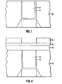
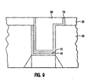
- a conductive via (CA) 15 in an oxide 20 there is shown a conductive via (CA) 15 in an oxide 20 .
- the conductive material will be Tungsten (W).
- W Tungsten
- the next level metal wires can now be created by a conventional damascene process which starts out with the deposition of a low-k dielectric film (M1 dielectric) 30 followed by the deposition of an oxide hardmask (M1 Hardmask) 40 and Ml photoresist 50 .
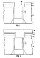
- FIG. 3 there is shown the transfer of the Ml line pattern 60 into the dielectric 30 by Reactive Ion Etching (RIE) including a resist strip.
- RIE Reactive Ion Etching
- Figure 4 there is shown the conventional processing step of liner/seed/plating to form liner 70 and Ml wiring metal 80 .
- Figure 5 there is shown the last conventional processing step of CMP to form the Ml wiring 90 .
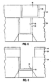
- the present invention can be used with the same dielectric deposition steps of the low-k material 30 and oxide hardmask 40 , followed by the same lithography step as illustrated in Figure 2 .
- the present invention deviates from the known art either during or after the RIE step.
- a first embodiment of the present invention is to use a fluorine containing gas (but not a fluorocarbon based gas) such as NF3, F2 or SF6 to selectively etch the low-k dielectric 30 to oxide 20 .
- a fluorine containing gas such as NF3, F2 or SF6
- the low-k dielectric 30 is a SiCOH-like material, and could be a porous-ULK material.
- the resist selectivity during this RIE step will be low and the critical dimension (CD) control in this case is provided by the oxide hardmask 40 which exhibits a low etch rate in these fluorine-based chemistries.
- the fluorine based chemistry can also etch the CA tungsten 15 as well as the CA liner 10 . Therefore, the low-k over etch can be used to recess the CA tungsten via to the desired depth. Since the etch rate of resist is high in these chemistries, it can be completely consumed before or during the low-k over etch and no additional resist strip is required.
- This selective Ml RIE process is compatible with conventional etch tools such as parallel plate and medium density plasma RIE tools.
- the etch gases comprise approximately 500 sccm of Ar and approximately 50 sccm of NF 3 .
- small amounts of O 2 and CH 2 F 2 or CH 3 F may be added.
- the latter additions can help maintain the critical dimensions or increase the selectivity to the oxide hardmask or resist.
- the pressure is approximately 100 to 200 mTorr with a power of about 500W for both 27 and 2 MHz frequencies.
- Another example not being part of the present invention is to follow known art after the lithography step.
- fluorine-based chemistry NF3, F2, SF6
- the fluorine-based chemistry NF3, F2, SF6
- the known art is followed after the lithography step.
- the next step would be to recess the CA tungsten 15 and liner 10 which also strips the remaining photoresist materials 50 .
- Figure 6 shows the final results in cross section.
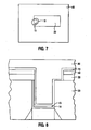
- Figure 7 shows a top-down view for these three embodiments illustrating the partially exposed CA tungsten 15 and liner 10 in the recessed trench formed in the low-k dielectric 30 and oxide hardmask 40 .
- the metallization of this structure is achieved by the known art discussed above.
- the CA stud interconnect is now a composite structure of two conductive materials.
- the conductive materials are Tungsten and Copper.
- the composite stud structure is approximately 100 nanometers in width and approximately 2,000 angstroms in height and the Tungsten portion is approximately 500 angstroms in height.
- This composite CA stud contact will have a lower contact resistance than a conventional contact.
- a 2,000 angstrom high and 95nm wide conventional Tungsten CA stud has an estimated contact resistance of 19 ohms. Approximately a third of this resistance is from W conductivity. If the Tungsten CA is etch backed to a 500 angstrom height, the contact resistance will drop from 19 to 13 ohms.
- Another advantage is that the contact area between any misaligned (and recessed) CA stud and the M1 line is increased. Besides a lower contact resistance between the copper line and the CA stud, this also provides a more reliable contact.
Landscapes
- Engineering & Computer Science (AREA)
- Physics & Mathematics (AREA)
- Condensed Matter Physics & Semiconductors (AREA)
- General Physics & Mathematics (AREA)
- Computer Hardware Design (AREA)
- Microelectronics & Electronic Packaging (AREA)
- Power Engineering (AREA)
- Manufacturing & Machinery (AREA)
- Chemical & Material Sciences (AREA)
- General Chemical & Material Sciences (AREA)
- Chemical Kinetics & Catalysis (AREA)
- Plasma & Fusion (AREA)
- Inorganic Chemistry (AREA)
- Internal Circuitry In Semiconductor Integrated Circuit Devices (AREA)
- Drying Of Semiconductors (AREA)
- Coupling Device And Connection With Printed Circuit (AREA)
- Connections Effected By Soldering, Adhesion, Or Permanent Deformation (AREA)
- Connections Arranged To Contact A Plurality Of Conductors (AREA)
Claims (8)
- Procédé de fabrication d'un dispositif électronique comprenant les étapes consistant à :fournir un substrat sur lequel des contacts doivent être formés,fournir une traversée conductrice (15) qui connecte l'un desdits contacts, la traversée conductrice comprenant un premier matériau conducteur formé dans un oxyde (20) sur ledit substrat,fournir une couche diélectrique (30) sur ladite traversée conductrice (15), fournir une couche d'oxyde (40) sur ladite couche diélectrique (30), fournir une couche de résine photosensible (50) sur ladite couche d'oxyde (40), former des ouvertures dans ladite couche de résine photosensible (50),dans une même étape, éliminer ladite couche de résine photosensible (50) et éliminer dans lesdites ouvertures ladite couche diélectrique (30) et ladite couche d'oxyde (40) et une partie dudit premier matériau conducteur, en transférant de cette manière lesdites ouvertures dans ladite couche diélectrique (30) et ladite couche d'oxyde (40) et former un évidement dans ledit matériau conducteur, par attaque à ions réactifs avec un gaz contenant du fluor qui n'est pas un gaz à base de fluorocarbure avec optionnellement l'ajout de petites quantités de O2 et de CH2F2 ou de CH3F,déposer un deuxième matériau conducteur (80) dans lesdites ouvertures transférées et ledit évidement pour former une traversée conductrice composite comprenant ledit premier matériau conducteur et ledit deuxième matériau conducteur.
- Procédé de fabrication d'un dispositif électronique comprenant les étapes consistant à :fournir un substrat sur lequel des contacts doivent être formés,fournir une traversée conductrice (15) qui connecte l'un desdits contacts, la traversée conductrice comprenant un premier matériau conducteur formé dans un oxyde sur ledit substrat,fournir une couche diélectrique (30) sur ladite traversée conductrice (15), fournir une couche d'oxyde (40) sur ladite couche diélectrique (30), fournir une couche de résine photosensible (50) sur ladite couche d'oxyde (40), former des ouvertures dans ladite couche de résine photosensible (50),éliminer dans lesdites ouvertures ladite couche diélectrique (30) et ladite couche d'oxyde (40) avec un gaz contenant du fluorocarbure, en transférant de cette manière lesdites ouvertures dans ladite couche diélectrique (30) et ladite couche d'oxyde (40),dans une même étape, éliminer ladite couche de résine photosensible (50) et éliminer dans lesdites ouvertures une partie de ladite première couche conductrice en formant de cette manière un évidement, utiliser une attaque à ions réactifs avec un gaz contenant du fluor qui n'est pas un gaz à base de fluorocarbure avec optionnellement l'ajout de petites quantités de O2 et de CH2F2 ou de CH3F,déposer un deuxième matériau conducteur (80) dans lesdites ouvertures transférées et ledit évidement pour former une traversée conductrice composite comprenant ledit premier matériau conducteur et ledit deuxième matériau conducteur.
- Procédé selon l'une quelconque des revendications précédentes, dans lequel ledit gaz contenant du fluor est sélectionné à partir du groupe constitué de NF3, F2 et SF6.
- Procédé selon la revendication 1 ou la revendication 2, dans lequel ladite couche diélectrique (30) est un matériau SiCOH à faible K.
- Procédé selon la revendication 4, dans lequel ledit matériau SiCOH à faible K est un matériau poreux à K ultra faible.
- Procédé selon la revendication 1 ou la revendication 2, dans lequel ledit premier matériau conducteur est le Tungstène et ledit deuxième matériau conducteur (80) est le Cuivre.
- Procédé selon la revendication 6, dans lequel ladite élimination de gaz contenant du fluor comprend approximativement 500 sccm d'Argon et approximativement 50 sccm de NF3.
- Procédé selon la revendication 7, dans lequel ladite élimination de gaz contenant du fluor comprend en outre approximativement 10 sccm de O2 et 50 sccm de CH2F2 ou de CH3F.
Applications Claiming Priority (2)
| Application Number | Priority Date | Filing Date | Title |
|---|---|---|---|
| US11/161,538 US7323410B2 (en) | 2005-08-08 | 2005-08-08 | Dry etchback of interconnect contacts |
| PCT/EP2006/064757 WO2007017400A1 (fr) | 2005-08-08 | 2006-07-27 | Rétrogravure à sec des contacts d'interconnexion |
Publications (2)
| Publication Number | Publication Date |
|---|---|
| EP1922753A1 EP1922753A1 (fr) | 2008-05-21 |
| EP1922753B1 true EP1922753B1 (fr) | 2011-03-30 |
Family
ID=37074972
Family Applications (1)
| Application Number | Title | Priority Date | Filing Date |
|---|---|---|---|
| EP06778036A Not-in-force EP1922753B1 (fr) | 2005-08-08 | 2006-07-27 | Gravure sèche en retrait de contacts d'interconnexion |
Country Status (9)
| Country | Link |
|---|---|
| US (2) | US7323410B2 (fr) |
| EP (1) | EP1922753B1 (fr) |
| JP (1) | JP4742147B2 (fr) |
| KR (1) | KR101027172B1 (fr) |
| CN (1) | CN101228624B (fr) |
| AT (1) | ATE504084T1 (fr) |
| DE (1) | DE602006021035D1 (fr) |
| TW (1) | TWI377618B (fr) |
| WO (1) | WO2007017400A1 (fr) |
Families Citing this family (12)
| Publication number | Priority date | Publication date | Assignee | Title |
|---|---|---|---|---|
| US20070037316A1 (en) * | 2005-08-09 | 2007-02-15 | Micron Technology, Inc. | Memory cell contact using spacers |
| US20070232048A1 (en) * | 2006-03-31 | 2007-10-04 | Koji Miyata | Damascene interconnection having a SiCOH low k layer |
| US8399349B2 (en) * | 2006-04-18 | 2013-03-19 | Air Products And Chemicals, Inc. | Materials and methods of forming controlled void |
| US7935640B2 (en) * | 2007-08-10 | 2011-05-03 | Tokyo Electron Limited | Method for forming a damascene structure |
| US7947609B2 (en) * | 2007-08-10 | 2011-05-24 | Tokyo Electron Limited | Method for etching low-k material using an oxide hard mask |
| US8080473B2 (en) * | 2007-08-29 | 2011-12-20 | Tokyo Electron Limited | Method for metallizing a pattern in a dielectric film |
| JP5102720B2 (ja) * | 2008-08-25 | 2012-12-19 | 東京エレクトロン株式会社 | 基板処理方法 |
| US8435901B2 (en) | 2010-06-11 | 2013-05-07 | Tokyo Electron Limited | Method of selectively etching an insulation stack for a metal interconnect |
| KR102057855B1 (ko) | 2013-11-13 | 2019-12-20 | 삼성전자 주식회사 | 반도체 소자 및 그 제조 방법 |
| US9514977B2 (en) | 2013-12-17 | 2016-12-06 | Kabushiki Kaisha Toshiba | Semiconductor device and manufacturing method thereof |
| US9484401B2 (en) | 2014-11-24 | 2016-11-01 | International Business Machines Corporation | Capacitance reduction for advanced technology nodes |
| US9679807B1 (en) * | 2015-11-20 | 2017-06-13 | Globalfoundries Inc. | Method, apparatus, and system for MOL interconnects without titanium liner |
Family Cites Families (26)
| Publication number | Priority date | Publication date | Assignee | Title |
|---|---|---|---|---|
| US4808552A (en) | 1985-09-11 | 1989-02-28 | Texas Instruments Incorporated | Process for making vertically-oriented interconnections for VLSI devices |
| US4793897A (en) * | 1987-03-20 | 1988-12-27 | Applied Materials, Inc. | Selective thin film etch process |
| US5244534A (en) * | 1992-01-24 | 1993-09-14 | Micron Technology, Inc. | Two-step chemical mechanical polishing process for producing flush and protruding tungsten plugs |
| US5300813A (en) | 1992-02-26 | 1994-04-05 | International Business Machines Corporation | Refractory metal capped low resistivity metal conductor lines and vias |
| JPH05267241A (ja) * | 1992-03-18 | 1993-10-15 | Fujitsu Ltd | 半導体装置の製造方法 |
| DE69213928T2 (de) | 1992-05-27 | 1997-03-13 | Sgs Thomson Microelectronics | Verdrahtung auf Wolfram-Plomben |
| JPH06260441A (ja) * | 1993-03-03 | 1994-09-16 | Nec Corp | 半導体装置の製造方法 |
| US5413670A (en) * | 1993-07-08 | 1995-05-09 | Air Products And Chemicals, Inc. | Method for plasma etching or cleaning with diluted NF3 |
| FR2754391B1 (fr) * | 1996-10-08 | 1999-04-16 | Sgs Thomson Microelectronics | Structure de contact a facteur de forme eleve pour circuits integres |
| US5970374A (en) | 1996-10-18 | 1999-10-19 | Chartered Semiconductor Manufacturing Ltd. | Method for forming contacts and vias with improved barrier metal step-coverage |
| JPH10242271A (ja) * | 1997-02-28 | 1998-09-11 | Sony Corp | 半導体装置及びその製造方法 |
| US6043163A (en) * | 1997-12-29 | 2000-03-28 | Taiwan Semiconductor Manufacturing Company, Ltd. | HCL in overetch with hard mask to improve metal line etching profile |
| WO1999050903A1 (fr) * | 1998-03-30 | 1999-10-07 | Hitachi, Ltd. | Circuit integre a semi-conducteur et procede de fabrication correspondant |
| TW377502B (en) | 1998-05-26 | 1999-12-21 | United Microelectronics Corp | Method of dual damascene |
| JP4809961B2 (ja) * | 1998-08-07 | 2011-11-09 | 株式会社東芝 | 半導体装置及びその製造方法 |
| US6040243A (en) * | 1999-09-20 | 2000-03-21 | Chartered Semiconductor Manufacturing Ltd. | Method to form copper damascene interconnects using a reverse barrier metal scheme to eliminate copper diffusion |
| JP3400770B2 (ja) * | 1999-11-16 | 2003-04-28 | 松下電器産業株式会社 | エッチング方法、半導体装置及びその製造方法 |
| US6534389B1 (en) | 2000-03-09 | 2003-03-18 | International Business Machines Corporation | Dual level contacts and method for forming |
| US6753249B1 (en) | 2001-01-16 | 2004-06-22 | Taiwan Semiconductor Manufacturing Company | Multilayer interface in copper CMP for low K dielectric |
| US6566242B1 (en) * | 2001-03-23 | 2003-05-20 | International Business Machines Corporation | Dual damascene copper interconnect to a damascene tungsten wiring level |
| US6426558B1 (en) | 2001-05-14 | 2002-07-30 | International Business Machines Corporation | Metallurgy for semiconductor devices |
| US20020171147A1 (en) * | 2001-05-15 | 2002-11-21 | Tri-Rung Yew | Structure of a dual damascene via |
| JP2003068848A (ja) * | 2001-08-29 | 2003-03-07 | Fujitsu Ltd | 半導体装置及びその製造方法 |
| TW544916B (en) * | 2002-01-10 | 2003-08-01 | Winbond Electronics Corp | Memory device having complex type contact plug and its manufacturing method |
| US6867073B1 (en) * | 2003-10-21 | 2005-03-15 | Ziptronix, Inc. | Single mask via method and device |
| US7030468B2 (en) * | 2004-01-16 | 2006-04-18 | International Business Machines Corporation | Low k and ultra low k SiCOH dielectric films and methods to form the same |
-
2005
- 2005-08-08 US US11/161,538 patent/US7323410B2/en active Active
-
2006
- 2006-07-27 DE DE602006021035T patent/DE602006021035D1/de active Active
- 2006-07-27 WO PCT/EP2006/064757 patent/WO2007017400A1/fr active Application Filing
- 2006-07-27 JP JP2008525532A patent/JP4742147B2/ja not_active Expired - Fee Related
- 2006-07-27 EP EP06778036A patent/EP1922753B1/fr not_active Not-in-force
- 2006-07-27 AT AT06778036T patent/ATE504084T1/de not_active IP Right Cessation
- 2006-07-27 CN CN2006800270555A patent/CN101228624B/zh not_active Expired - Fee Related
- 2006-07-27 KR KR1020087002079A patent/KR101027172B1/ko not_active IP Right Cessation
- 2006-08-01 TW TW095128192A patent/TWI377618B/zh not_active IP Right Cessation
-
2007
- 2007-11-29 US US11/946,922 patent/US7645700B2/en not_active Expired - Fee Related
Also Published As
| Publication number | Publication date |
|---|---|
| US20070032055A1 (en) | 2007-02-08 |
| KR101027172B1 (ko) | 2011-04-05 |
| TWI377618B (en) | 2012-11-21 |
| CN101228624A (zh) | 2008-07-23 |
| US7323410B2 (en) | 2008-01-29 |
| KR20080033300A (ko) | 2008-04-16 |
| JP2009505385A (ja) | 2009-02-05 |
| JP4742147B2 (ja) | 2011-08-10 |
| TW200741849A (en) | 2007-11-01 |
| CN101228624B (zh) | 2011-07-20 |
| ATE504084T1 (de) | 2011-04-15 |
| EP1922753A1 (fr) | 2008-05-21 |
| US7645700B2 (en) | 2010-01-12 |
| WO2007017400A1 (fr) | 2007-02-15 |
| US20080088027A1 (en) | 2008-04-17 |
| DE602006021035D1 (de) | 2011-05-12 |
Similar Documents
| Publication | Publication Date | Title |
|---|---|---|
| EP1922753B1 (fr) | Gravure sèche en retrait de contacts d'interconnexion | |
| US10879178B2 (en) | Electrically conductive laminate structures | |
| US6713402B2 (en) | Methods for polymer removal following etch-stop layer etch | |
| US7871923B2 (en) | Self-aligned air-gap in interconnect structures | |
| US7655547B2 (en) | Metal spacer in single and dual damascene processing | |
| US7629264B2 (en) | Structure and method for hybrid tungsten copper metal contact | |
| JP2009510771A (ja) | 導電性キャッピング層を含む銅ベースのメタライゼーション層を形成する技術 | |
| US20030181034A1 (en) | Methods for forming vias and trenches with controlled SiC etch rate and selectivity | |
| CN104517894A (zh) | 半导体结构及其形成方法 | |
| EP1460677A2 (fr) | Gravure d'une couche BARC avec une composition à attaque selective et un gaz hautement polymérisant pour la contrôle de la dimension critique (CD) | |
| KR100419021B1 (ko) | 반도체소자의 구리 배선 제조방법 | |
| US6236091B1 (en) | Method of forming a local interconnect with improved etch selectivity of silicon dioxide/silicide | |
| JP2005005697A (ja) | 半導体装置の製造方法 | |
| KR100909174B1 (ko) | 듀얼 다마신 패턴 형성 방법 | |
| TWI512894B (zh) | 金屬內連線結構及其製程 | |
| CN113097127B (zh) | 半导体结构的形成方法 | |
| KR20010025972A (ko) | 반도체 장치의 배선 형성방법 | |
| KR100928107B1 (ko) | 반도체 소자 및 그 제조 방법 | |
| KR20070052452A (ko) | 반도체 소자의 금속배선 제조방법 | |
| JP2003174085A (ja) | デュアルダマシン構造体及びその形成方法、並びに半導体装置及びその製造方法 |
Legal Events
| Date | Code | Title | Description |
|---|---|---|---|
| PUAI | Public reference made under article 153(3) epc to a published international application that has entered the european phase |
Free format text: ORIGINAL CODE: 0009012 |
|
| 17P | Request for examination filed |
Effective date: 20080225 |
|
| AK | Designated contracting states |
Kind code of ref document: A1 Designated state(s): AT BE BG CH CY CZ DE DK EE ES FI FR GB GR HU IE IS IT LI LT LU LV MC NL PL PT RO SE SI SK TR |
|
| RIN1 | Information on inventor provided before grant (corrected) |
Inventor name: STANDAERT, THEODORUS Inventor name: SANKARAN, SUJATHA,C/O IBM UNITED KINGDOM LIMITED Inventor name: BREARLEY, WILLIAM Inventor name: GRECO, STEPHEN |
|
| 17Q | First examination report despatched |
Effective date: 20080808 |
|
| GRAP | Despatch of communication of intention to grant a patent |
Free format text: ORIGINAL CODE: EPIDOSNIGR1 |
|
| GRAS | Grant fee paid |
Free format text: ORIGINAL CODE: EPIDOSNIGR3 |
|
| GRAA | (expected) grant |
Free format text: ORIGINAL CODE: 0009210 |
|
| AK | Designated contracting states |
Kind code of ref document: B1 Designated state(s): AT BE BG CH CY CZ DE DK EE ES FI FR GB GR HU IE IS IT LI LT LU LV MC NL PL PT RO SE SI SK TR |
|
| REG | Reference to a national code |
Ref country code: GB Ref legal event code: FG4D |
|
| REG | Reference to a national code |
Ref country code: CH Ref legal event code: EP |
|
| REG | Reference to a national code |
Ref country code: DE Ref legal event code: R084 Ref document number: 602006021035 Country of ref document: DE |
|
| REG | Reference to a national code |
Ref country code: IE Ref legal event code: FG4D |
|
| REG | Reference to a national code |
Ref country code: GB Ref legal event code: 746 Effective date: 20110412 |
|
| REF | Corresponds to: |
Ref document number: 602006021035 Country of ref document: DE Date of ref document: 20110512 Kind code of ref document: P |
|
| REG | Reference to a national code |
Ref country code: DE Ref legal event code: R096 Ref document number: 602006021035 Country of ref document: DE Effective date: 20110512 |
|
| REG | Reference to a national code |
Ref country code: NL Ref legal event code: VDEP Effective date: 20110330 |
|
| PG25 | Lapsed in a contracting state [announced via postgrant information from national office to epo] |
Ref country code: LT Free format text: LAPSE BECAUSE OF FAILURE TO SUBMIT A TRANSLATION OF THE DESCRIPTION OR TO PAY THE FEE WITHIN THE PRESCRIBED TIME-LIMIT Effective date: 20110330 Ref country code: LV Free format text: LAPSE BECAUSE OF FAILURE TO SUBMIT A TRANSLATION OF THE DESCRIPTION OR TO PAY THE FEE WITHIN THE PRESCRIBED TIME-LIMIT Effective date: 20110330 Ref country code: SE Free format text: LAPSE BECAUSE OF FAILURE TO SUBMIT A TRANSLATION OF THE DESCRIPTION OR TO PAY THE FEE WITHIN THE PRESCRIBED TIME-LIMIT Effective date: 20110330 Ref country code: GR Free format text: LAPSE BECAUSE OF FAILURE TO SUBMIT A TRANSLATION OF THE DESCRIPTION OR TO PAY THE FEE WITHIN THE PRESCRIBED TIME-LIMIT Effective date: 20110701 |
|
| LTIE | Lt: invalidation of european patent or patent extension |
Effective date: 20110330 |
|
| PG25 | Lapsed in a contracting state [announced via postgrant information from national office to epo] |
Ref country code: FI Free format text: LAPSE BECAUSE OF FAILURE TO SUBMIT A TRANSLATION OF THE DESCRIPTION OR TO PAY THE FEE WITHIN THE PRESCRIBED TIME-LIMIT Effective date: 20110330 Ref country code: CY Free format text: LAPSE BECAUSE OF FAILURE TO SUBMIT A TRANSLATION OF THE DESCRIPTION OR TO PAY THE FEE WITHIN THE PRESCRIBED TIME-LIMIT Effective date: 20110330 Ref country code: AT Free format text: LAPSE BECAUSE OF FAILURE TO SUBMIT A TRANSLATION OF THE DESCRIPTION OR TO PAY THE FEE WITHIN THE PRESCRIBED TIME-LIMIT Effective date: 20110330 Ref country code: SI Free format text: LAPSE BECAUSE OF FAILURE TO SUBMIT A TRANSLATION OF THE DESCRIPTION OR TO PAY THE FEE WITHIN THE PRESCRIBED TIME-LIMIT Effective date: 20110330 |
|
| PG25 | Lapsed in a contracting state [announced via postgrant information from national office to epo] |
Ref country code: BE Free format text: LAPSE BECAUSE OF FAILURE TO SUBMIT A TRANSLATION OF THE DESCRIPTION OR TO PAY THE FEE WITHIN THE PRESCRIBED TIME-LIMIT Effective date: 20110330 |
|
| PG25 | Lapsed in a contracting state [announced via postgrant information from national office to epo] |
Ref country code: PT Free format text: LAPSE BECAUSE OF FAILURE TO SUBMIT A TRANSLATION OF THE DESCRIPTION OR TO PAY THE FEE WITHIN THE PRESCRIBED TIME-LIMIT Effective date: 20110801 Ref country code: EE Free format text: LAPSE BECAUSE OF FAILURE TO SUBMIT A TRANSLATION OF THE DESCRIPTION OR TO PAY THE FEE WITHIN THE PRESCRIBED TIME-LIMIT Effective date: 20110330 |
|
| PGFP | Annual fee paid to national office [announced via postgrant information from national office to epo] |
Ref country code: FR Payment date: 20110801 Year of fee payment: 6 |
|
| PG25 | Lapsed in a contracting state [announced via postgrant information from national office to epo] |
Ref country code: IS Free format text: LAPSE BECAUSE OF FAILURE TO SUBMIT A TRANSLATION OF THE DESCRIPTION OR TO PAY THE FEE WITHIN THE PRESCRIBED TIME-LIMIT Effective date: 20110730 Ref country code: SK Free format text: LAPSE BECAUSE OF FAILURE TO SUBMIT A TRANSLATION OF THE DESCRIPTION OR TO PAY THE FEE WITHIN THE PRESCRIBED TIME-LIMIT Effective date: 20110330 Ref country code: CZ Free format text: LAPSE BECAUSE OF FAILURE TO SUBMIT A TRANSLATION OF THE DESCRIPTION OR TO PAY THE FEE WITHIN THE PRESCRIBED TIME-LIMIT Effective date: 20110330 Ref country code: RO Free format text: LAPSE BECAUSE OF FAILURE TO SUBMIT A TRANSLATION OF THE DESCRIPTION OR TO PAY THE FEE WITHIN THE PRESCRIBED TIME-LIMIT Effective date: 20110330 Ref country code: ES Free format text: LAPSE BECAUSE OF FAILURE TO SUBMIT A TRANSLATION OF THE DESCRIPTION OR TO PAY THE FEE WITHIN THE PRESCRIBED TIME-LIMIT Effective date: 20110711 |
|
| PG25 | Lapsed in a contracting state [announced via postgrant information from national office to epo] |
Ref country code: NL Free format text: LAPSE BECAUSE OF FAILURE TO SUBMIT A TRANSLATION OF THE DESCRIPTION OR TO PAY THE FEE WITHIN THE PRESCRIBED TIME-LIMIT Effective date: 20110330 |
|
| PLBE | No opposition filed within time limit |
Free format text: ORIGINAL CODE: 0009261 |
|
| STAA | Information on the status of an ep patent application or granted ep patent |
Free format text: STATUS: NO OPPOSITION FILED WITHIN TIME LIMIT |
|
| PG25 | Lapsed in a contracting state [announced via postgrant information from national office to epo] |
Ref country code: MC Free format text: LAPSE BECAUSE OF NON-PAYMENT OF DUE FEES Effective date: 20110731 Ref country code: DK Free format text: LAPSE BECAUSE OF FAILURE TO SUBMIT A TRANSLATION OF THE DESCRIPTION OR TO PAY THE FEE WITHIN THE PRESCRIBED TIME-LIMIT Effective date: 20110330 Ref country code: PL Free format text: LAPSE BECAUSE OF FAILURE TO SUBMIT A TRANSLATION OF THE DESCRIPTION OR TO PAY THE FEE WITHIN THE PRESCRIBED TIME-LIMIT Effective date: 20110330 |
|
| REG | Reference to a national code |
Ref country code: CH Ref legal event code: PL |
|
| 26N | No opposition filed |
Effective date: 20120102 |
|
| REG | Reference to a national code |
Ref country code: IE Ref legal event code: MM4A |
|
| REG | Reference to a national code |
Ref country code: DE Ref legal event code: R097 Ref document number: 602006021035 Country of ref document: DE Effective date: 20120102 |
|
| PG25 | Lapsed in a contracting state [announced via postgrant information from national office to epo] |
Ref country code: LI Free format text: LAPSE BECAUSE OF NON-PAYMENT OF DUE FEES Effective date: 20110731 Ref country code: CH Free format text: LAPSE BECAUSE OF NON-PAYMENT OF DUE FEES Effective date: 20110731 |
|
| PG25 | Lapsed in a contracting state [announced via postgrant information from national office to epo] |
Ref country code: IT Free format text: LAPSE BECAUSE OF FAILURE TO SUBMIT A TRANSLATION OF THE DESCRIPTION OR TO PAY THE FEE WITHIN THE PRESCRIBED TIME-LIMIT Effective date: 20110330 |
|
| PG25 | Lapsed in a contracting state [announced via postgrant information from national office to epo] |
Ref country code: IE Free format text: LAPSE BECAUSE OF NON-PAYMENT OF DUE FEES Effective date: 20110727 |
|
| REG | Reference to a national code |
Ref country code: FR Ref legal event code: ST Effective date: 20130329 |
|
| PG25 | Lapsed in a contracting state [announced via postgrant information from national office to epo] |
Ref country code: FR Free format text: LAPSE BECAUSE OF NON-PAYMENT OF DUE FEES Effective date: 20120731 |
|
| PG25 | Lapsed in a contracting state [announced via postgrant information from national office to epo] |
Ref country code: LU Free format text: LAPSE BECAUSE OF NON-PAYMENT OF DUE FEES Effective date: 20110727 |
|
| PG25 | Lapsed in a contracting state [announced via postgrant information from national office to epo] |
Ref country code: BG Free format text: LAPSE BECAUSE OF FAILURE TO SUBMIT A TRANSLATION OF THE DESCRIPTION OR TO PAY THE FEE WITHIN THE PRESCRIBED TIME-LIMIT Effective date: 20110630 |
|
| PG25 | Lapsed in a contracting state [announced via postgrant information from national office to epo] |
Ref country code: TR Free format text: LAPSE BECAUSE OF FAILURE TO SUBMIT A TRANSLATION OF THE DESCRIPTION OR TO PAY THE FEE WITHIN THE PRESCRIBED TIME-LIMIT Effective date: 20110330 |
|
| PG25 | Lapsed in a contracting state [announced via postgrant information from national office to epo] |
Ref country code: HU Free format text: LAPSE BECAUSE OF FAILURE TO SUBMIT A TRANSLATION OF THE DESCRIPTION OR TO PAY THE FEE WITHIN THE PRESCRIBED TIME-LIMIT Effective date: 20110330 |
|
| PGFP | Annual fee paid to national office [announced via postgrant information from national office to epo] |
Ref country code: GB Payment date: 20150722 Year of fee payment: 10 |
|
| REG | Reference to a national code |
Ref country code: DE Ref legal event code: R081 Ref document number: 602006021035 Country of ref document: DE Owner name: AURIGA INNOVATIONS, INC.,, OTTAWA, CA Free format text: FORMER OWNER: INTERNATIONAL BUSINESS MACHINES CORPORATION, ARMONK, NY, US Ref country code: DE Ref legal event code: R082 Ref document number: 602006021035 Country of ref document: DE Representative=s name: RICHARDT PATENTANWAELTE PARTG MBB, DE Ref country code: DE Ref legal event code: R081 Ref document number: 602006021035 Country of ref document: DE Owner name: GLOBALFOUNDRIES INC., KY Free format text: FORMER OWNER: INTERNATIONAL BUSINESS MACHINES CORPORATION, ARMONK, N.Y., US Ref country code: DE Ref legal event code: R081 Ref document number: 602006021035 Country of ref document: DE Owner name: AURIGA INNOVATIONS, INC.,, OTTAWA, CA Free format text: FORMER OWNER: INTERNATIONAL BUSINESS MACHINES CORPORATION, ARMONK, N.Y., US |
|
| REG | Reference to a national code |
Ref country code: DE Ref legal event code: R082 Ref document number: 602006021035 Country of ref document: DE Representative=s name: RICHARDT PATENTANWAELTE PARTG MBB, DE Ref country code: DE Ref legal event code: R081 Ref document number: 602006021035 Country of ref document: DE Owner name: GLOBALFOUNDRIES INC., KY Free format text: FORMER OWNER: GLOBALFOUNDRIES US 2 LLC (N.D.GES.DES STAATES DELAWARE), HOPEWELL JUNCTION, N.Y., US Ref country code: DE Ref legal event code: R081 Ref document number: 602006021035 Country of ref document: DE Owner name: AURIGA INNOVATIONS, INC.,, OTTAWA, CA Free format text: FORMER OWNER: GLOBALFOUNDRIES US 2 LLC (N.D.GES.DES STAATES DELAWARE), HOPEWELL JUNCTION, N.Y., US |
|
| REG | Reference to a national code |
Ref country code: FR Ref legal event code: TP Owner name: GLOBALFOUNDRIES INC., GB Effective date: 20160829 |
|
| GBPC | Gb: european patent ceased through non-payment of renewal fee |
Effective date: 20160727 |
|
| PG25 | Lapsed in a contracting state [announced via postgrant information from national office to epo] |
Ref country code: GB Free format text: LAPSE BECAUSE OF NON-PAYMENT OF DUE FEES Effective date: 20160727 |
|
| REG | Reference to a national code |
Ref country code: DE Ref legal event code: R082 Ref document number: 602006021035 Country of ref document: DE Representative=s name: RICHARDT PATENTANWAELTE PARTG MBB, DE Ref country code: DE Ref legal event code: R081 Ref document number: 602006021035 Country of ref document: DE Owner name: AURIGA INNOVATIONS, INC.,, OTTAWA, CA Free format text: FORMER OWNER: GLOBALFOUNDRIES INC., GRAND CAYMAN, KY |
|
| PGFP | Annual fee paid to national office [announced via postgrant information from national office to epo] |
Ref country code: DE Payment date: 20200714 Year of fee payment: 15 |
|
| REG | Reference to a national code |
Ref country code: DE Ref legal event code: R119 Ref document number: 602006021035 Country of ref document: DE |
|
| PG25 | Lapsed in a contracting state [announced via postgrant information from national office to epo] |
Ref country code: DE Free format text: LAPSE BECAUSE OF NON-PAYMENT OF DUE FEES Effective date: 20220201 |