EP1921663B1 - Tube à électrons et procédé de fabrication d un tube à électrons - Google Patents
Tube à électrons et procédé de fabrication d un tube à électrons Download PDFInfo
- Publication number
- EP1921663B1 EP1921663B1 EP06767519.9A EP06767519A EP1921663B1 EP 1921663 B1 EP1921663 B1 EP 1921663B1 EP 06767519 A EP06767519 A EP 06767519A EP 1921663 B1 EP1921663 B1 EP 1921663B1
- Authority
- EP
- European Patent Office
- Prior art keywords
- metal film
- photocathode
- envelope
- opening
- multilayer metal
- Prior art date
- Legal status (The legal status is an assumption and is not a legal conclusion. Google has not performed a legal analysis and makes no representation as to the accuracy of the status listed.)
- Active
Links
Images


Classifications
-
- H—ELECTRICITY
- H01—ELECTRIC ELEMENTS
- H01J—ELECTRIC DISCHARGE TUBES OR DISCHARGE LAMPS
- H01J43/00—Secondary-emission tubes; Electron-multiplier tubes
- H01J43/04—Electron multipliers
- H01J43/28—Vessels, e.g. wall of the tube; Windows; Screens; Suppressing undesired discharges or currents
-
- H—ELECTRICITY
- H01—ELECTRIC ELEMENTS
- H01J—ELECTRIC DISCHARGE TUBES OR DISCHARGE LAMPS
- H01J5/00—Details relating to vessels or to leading-in conductors common to two or more basic types of discharge tubes or lamps
- H01J5/20—Seals between parts of vessels
- H01J5/22—Vacuum-tight joints between parts of vessel
- H01J5/24—Vacuum-tight joints between parts of vessel between insulating parts of vessel
-
- H—ELECTRICITY
- H01—ELECTRIC ELEMENTS
- H01J—ELECTRIC DISCHARGE TUBES OR DISCHARGE LAMPS
- H01J9/00—Apparatus or processes specially adapted for the manufacture, installation, removal, maintenance of electric discharge tubes, discharge lamps, or parts thereof; Recovery of material from discharge tubes or lamps
- H01J9/24—Manufacture or joining of vessels, leading-in conductors or bases
- H01J9/26—Sealing together parts of vessels
Definitions
- the present invention relates to an electron tube which generates a photoelectron in response to light incident thereon from the outside, and a method of making the same.
- Electron tubes such as phototubes and photomultiplier tubes (PMT) have conventionally been known as photosensors. These electron tubes are constructed such that a photocathode which converts light into an electron and an anode are provided within a vacuum container.
- An example of such electron tubes is a photomultiplier tube in which a component having an inner face formed with a photocathode, a component formed with a photomultiplier part, and a component having an inner face formed with an anode are joined together (see the following Patent Document 1).
- US 5 568 013 A relates to a micro-fabricated electron multiplier.
- JP 2004 226632 A relates to a joint substrate, an optical substrate and its manufacturing method.
- the electron tube in accordance with claim 1 is an electron tube comprising an envelope including a side tube having at least one end part formed with an opening and a joining member airtightly joined to the opening, and a photocathode contained within the envelope, the photocathode emitting a photoelectron into the envelope in response to light incident thereon from the outside; wherein a multilayer metal film constituted by a metal film made of titanium, a metal film made of platinum, and a metal film made of gold successively laminated toward a joining direction is formed in each of the opening and a joint part of the joining member with the opening; and wherein the side tube and the joining member are joined to each other by holding a joint material containing indium between the respective multilayer metal films.
- a side tube and a joining member are joined to each other by holding a joint material containing indium between multilayer metal films each containing titanium, platinum, and gold in this order, so as to form an envelope, within which a photocathode emitting a photoelectron in response to light from the outside is provided.
- a joint material containing indium between multilayer metal films each containing titanium, platinum, and gold in this order, so as to form an envelope, within which a photocathode emitting a photoelectron in response to light from the outside is provided.
- the method of making an electron tube in accordance with claim 4 the present invention is a method of making an electron tube including a photocathode emitting a photocathode into an envelope in response to light incident thereon from the outside within the envelope, the method comprising the steps of preparing a side tube constituting a part of the envelope and having one end part formed with an opening; forming the opening with a metal film made of titanium, a metal film made of platinum, and a metal film made of gold in succession; preparing a joining member, to be joined to the opening, constituting a part of the envelope; forming a metal film made of titanium, a metal film made of platinum, and a metal film made of gold in succession at a joint part of the joining member with the opening; forming the photocathode within the side tube or within the joining member; and joining the opening of the side tube and the joining member to each other by holding a joint material containing indium therebetween.
- the electron tube and method of making the same in accordance with the present invention can sufficiently keep the airtightness within small-sized vacuum containers.
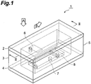
- Fig. 1 is a perspective view showing the structure of a photomultiplier tube 1 which is an embodiment of the electron tube in accordance with the present invention.
- the photomultiplier tube 1 is a transmission type electron multiplier tube having an envelope 5 constituted by an upper substrate 2, a frame 3, and a lower substrate 4, and is constructed by accommodating a photocathode 6, an electron multiplier part 7, and an anode 8 within the envelope 5.
- This photomultiplier tube 1 is a photomultiplier tube in which the incident direction of light onto the photocathode 6 and the electron traveling direction in the electron multiplier part 7 intersect.
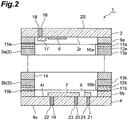
- the upper substrate 2 and lower substrate 4 are rectangular flat sheets made of glass, while the frame 3 is constituted by two frame-like members, each having a hollow quadrangular prism form, which are joined together along the substrate surface.
- the frame-like members are connected to marginal parts of the upper substrate 2 and lower substrate 4 such that the four sides of each substrate are parallel to the four sides of each frame-like member.
- the frame 3 is constituted by frames 3a and 3b as frame-like members. More specifically, the frame 3a connected to the upper substrate 2 has a frame body 9a made of silicon (Si) joined to the surface of the marginal part of the upper substrate 2 and a multilayer metal film 10a formed by laminating a metal film 11 a made of titanium (Ti), a metal film 12a made of platinum (Pt), and a metal film 13a made of gold (Au) on the frame body 9a in this order toward the lower substrate 4.
- An intermediate layer 15a made of aluminum or silicon oxide (SiO 2 ) is provided between the frame body 9a and multilayer metal film 10a.
- the frame 3b connected to the lower substrate 4 has a frame body 9b made of Si joined onto the surface of the marginal part of the lower substrate 4 and a multilayer metal film 10b formed by laminating a metal film 11b made of titanium, a metal film 12b made of platinum, and a metal film 13b made of gold on the frame body 9b in this order toward the upper substrate 2.
- An intermediate layer 15b made of aluminum or silicon oxide (SiO 2 ) is provided between the frame body 9b and multilayer metal film 10b.
- the thicknesses of the metal films are such that the metal films 11 a, 11b are 30 nm each, the metal films 12a, 12b are 20 nm each, and the metal films 13a, 13b are 1 ⁇ m each.
- the frames 3a, 3b have a structure forming respective openings defined by the end parts of the frame bodies 9a, 9b on the side opposite from the substrates 2, 4, while the openings are formed with the multilayer metal films 10a, 10b, respectively.
- the frames 3a and 3b are joined together by holding a joint material containing indium (In) (including In, alloys of In and Sn, alloys of In and Ag, and the like, for example) between the multilayer metal films 10a and 10b, whereby the inside is kept airtight.
- a joint layer 14 made of a joint material is formed on the multilayer metal film 10b in Fig. 2 , the joint layer may be formed on the multilayer metal film 10a as well.
- the upper substrate 2 including the frame 3a has a role as a joining member airtightly sealed to the opening of the frame 3b including the lower substrate 4 as a side tube
- the lower substrate 4 including the frame 3b has a role as a joining member airtightly sealed to the opening of the frame 3a including the upper substrate 2 as a side tube. Therefore, the multilayer metal films 10a, 10b are formed at the respective joint parts with the openings of the frames 3b, 3a, i.e., the marginal parts of the substrates 2, 4.
- the frame 3 may be constituted by one member made of Si instead of two members of the frames 3a and 3b.
- the frame 3 as a side tube is directly joined to the upper substrate 2 and lower substrate 4 acing as joining members.
- a multilayer metal film and a joint layer may be used for joining one or both of the upper substrate 2 and lower substrate 4 to the frame 3. It will be preferred in particular if the upper substrate 2 having the photocathode 6 and the frame 3 are joined together by a joint by a multilayer metal film and a joint layer after joining the lower substrate 4 and frame 3 to each other by anodic bonding.
- two members of the frames 3a and 3b are preferably provided as can be seen when taking account of steps of making the photomultiplier tube 1 which will be explained later.
- the inner face 2r of the upper substrate 2 in such an envelope 5 is formed with a transmission type photocathode 6 containing an alkali metal emitting a photoelectron into the envelope 5 in response to light incident thereon from the outside.
- the upper substrate 2 functions as a transmission window which transmits therethrough toward the photocathode 6 light incident thereon from the outside.
- the photocathode 6 is formed closer to an end part in the longitudinal direction (lateral direction in Fig. 2 ) of the inner face 2r of the upper substrate 2 along the inner face 2r.
- the upper substrate 2 is formed with a hole 16 penetrating therethrough from a surface 2s to the inner face 2r, while the Si layer 17 electrically connected to the photocathode 6 is formed on the inner face 2r side of the hole 16.
- a photocathode terminal 18 is arranged in the hole 16, and is electrically connected to the photocathode 6 by electrically coming into contact with the Si layer 17.
- the electron multiplier part 7 and anode 8 are formed along the inner face 4r.
- the electron multiplier part 7 has a plurality of wall parts erected so as to extend along each other in the longitudinal direction of the lower substrate 4, while a groove part is formed between the wall parts.
- the side walls and bottom parts of the wall parts are formed with secondary electron emissive surfaces made of a secondary electron emissive material.
- the electron multiplier part 7 is arranged at a position facing the photocathode 6 within the envelope 5.
- the anode 8 is provided at a position separated from the electron multiplier part 7.
- the lower substrate 4 is further provided with holes 19, 20, 21 penetrating therethrough from a surface 4s to the inner face 4r.
- a photocathode-side terminal 22, an anode-side terminal 23, and an anode terminal 24 are inserted in the holes 19, 20, and 21, respectively. Since the photocathode-side terminal 22 and anode-side terminal 23 are electrically in contact with both end parts of the electron multiplier part 7, respectively, a potential difference can be generated in the longitudinal direction of the lower substrate 4 by applying a predetermined voltage to the photocathode-side terminal 22 and anode-side terminal 23. Since the anode terminal 24 is electrically in contact with the anode 8, electrons having reached the anode 8 can be taken therefrom to the outside as a signal.
- the photoelectron having arrived at the electron multiplier part 7 is multiplied in a cascaded fashion while colliding with the side walls and bottom parts of the electron multiplier part 7, thereby reaching the anode 8 while generating secondary electrons.
- the generated secondary electrons are taken from the anode 8 to the outside through the anode terminal 24.
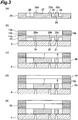
- an Si substrate 25 shaped like a rectangular flat sheet is prepared, and two terminals 29a, 29b for the electron multiplier part 7 and a terminal 29c for the anode 8 are formed on the surface of the Si substrate 25 by patterning aluminum.
- depressions 26 are processed by reactive ion etching (RIE) such as to form rectangular parallelepiped islands 27, 28 on a surface including the terminals 29a and 29b and a surface including the terminal 29c, respectively (area (a) in Fig. 3 ).
- RIE reactive ion etching
- the lower substrate 4 made of glass having already provided with the holes 19, 20, 21 for inserting terminals is prepared, and the Si substrate 25 and lower substrate 4 are joined together by anodic bonding such as to hold the terminals 29a, 29b, 29c therebetween.
- titanium, platinum, and gold are vapor-deposited in this order on the surface of the Si substrate 25, so as to produce the multilayer metal film 10b constituted by the metal films 11b, 12b, 13b, and the multilayer metal film 10b is formed at the marginal part on the surface of the Si substrate 25 by an etching process or liftoff process (area (b) in Fig. 3 ).
- the depressions 26 about the islands 27, 28 are penetrated through the Si substrate 25 to the surface thereof, so that the islands 27, 28 and the marginal part of the Si substrate 25 are formed as the electron multiplier part 7, anode 8, and frame body 9b, respectively (area (c) in Fig. 3 ).
- the frame body 9b may thereafter be treated at a high temperature for degassing thereof. In this case, depending on the processing temperature, the multilayer metal film 10b may become hard to keep. It will therefore be preferred if an intermediate layer made of aluminum or silicon oxide (SiO 2 ) is provided between the surface of the Si substrate 25 and the multilayer metal film 10b when forming the multilayer metal film 10b.
- the joint layer 14 to join with the opening of the upper substrate 2 including the frame 3a is vapor-deposited through a mask onto a surface of the metal film 10b acting as a joint part (area (d) in Fig. 3 ).
- a material containing In such as In, an alloy of In and Sn, or an alloy of In and Ag is used as the joint layer 14.
- the joint layer 14 may also be formed by printing a metal paste containing the above-mentioned joint material and then removing the binder contained in the metal paste by heating.
- an Si substrate 30 shaped like a rectangular flat sheet is prepared, and a terminal 33 for the photocathode 6 is formed on the surface of the Si substrate 30 by patterning aluminum. Thereafter, a depression 31 is processed by RIE such as to form a rectangular parallelepiped island 32 on the surface including the terminal 33 (area (a) in Fig. 4 ).
- the upper substrate 2 made of glass having already provided with the hole 16 for inserting a terminal is prepared, and the Si substrate 30 and upper substrate 2 are joined to each other by anodic bonding such as to hold the terminal 33 therebetween.
- titanium, platinum, and gold are vapor-deposited in this order on the surface of the Si substrate 30, so as to produce the multilayer metal film 10a constituted by the metal films 11a, 12a, 13a, and the multilayer metal film 10a is formed at the marginal part on the surface of the Si substrate 30 by an etching process or liftoff process (area (b) in Fig. 4 ).
- the depression 31 about the island 32 (see area (a) in Fig. 4 ) is penetrated through the Si substrate 30 to the surface thereof, so that the island 32 and the marginal part of the Si substrate 30 are formed as the Si layer 17 and frame body 9a, respectively (area (c) in Fig. 4 ).
- the frame body 9a may thereafter be treated at a high temperature for degassing thereof.
- the multilayer metal film 10a may become hard to keep. It will therefore be preferred if an intermediate layer made of aluminum or silicon oxide (SiO 2 ) is provided between the surface of the Si substrate 30 and the multilayer metal film 10a when forming the multilayer metal film 10a.
- a photocathode material containing antimony (Sb) is vapor-deposited through a mask onto the upper substrate 2 on the center part side with respect to the Si layer 17. Thereafter, an alkali metal is introduced, so as to form the photocathode 6 (area (d) in Fig. 4 ).
- the foregoing steps prepare the frame 3 a that forms a part of the envelope 5 and has one end part joined to the lower substrate 4 and the other end part formed with an opening.
- the frames 3a and 3b are joined together by aligning their openings with each other (area (e) in Fig. 4 ). This yields a state where the joint layer 14 is held between the multilayer metal films 10a, 10b, whereby the frames 3a and 3b are vacuum-sealed to each other when a joint material such as In is joined to the multilayer metal films 10a, 10b.
- the frames (side tubes) 3a, 3b are joined to their corresponding substrates (joining members) 4, 2 by holding a joint material containing indium between the multilayer metal films 10a, 10b each containing titanium, platinum, and gold in this order, so as to construct the envelope 5, within which the photocathode 6 emitting a photoelectron in response to light from the outside is provided.
- a joint material containing indium between the multilayer metal films 10a, 10b each containing titanium, platinum, and gold in this order, so as to construct the envelope 5, within which the photocathode 6 emitting a photoelectron in response to light from the outside is provided.
- Such a structure prevents metals such as Cr which are stabilized by oxidization in joint parts from being deposited, whereby the airtightness in the joint parts of the envelope 5 is stably kept even when reducing the size of the envelope 5.
- the structure holding the joint layer 14 between the multilayer metal films 10a, 10b is meaningful in terms of maintaining airtightness.
- the upper substrate 2 has its inner face formed with the photocathode 6, so that the ambient temperature can be kept in the same range from the making of the photocathode 6 to the joining of the envelope 5, and thus can be made efficiently.
- Fig. 5 is a graph showing elemental analysis results in the laminating direction of the multilayer metal film 10a in the photomultiplier tube 1
- Fig. 6 is a graph showing elemental analysis results in the laminating direction of a multilayer metal film in a photomultiplier tube which is a comparative example using a film laminating chromium (Cr) and gold (Au) in this order as the multilayer metal film.
- the elemental analyses were performed with an Auger electron spectrometer (AES).
- AES Auger electron spectrometer
- Table 1 also shows yields in Examples 1 and 2 of the present invention and Comparative Examples 1 to 5. These yields were determined according to whether or not the active state of the photocathode was kept after the making process.
- Table 1 UPPER SUBSTRATE MATERIAL UPPER MULTILAYER METAL FILM JOINT MATERIAL LOWER MULTILAYER METAL FILM LOWER SUBSTRATE MATERIAL YIELD EXAMPLE 1 GLASS Ti(30),Pt(20),Au(1000) InSn SHEET Ti(30),Pt(20),Au(1000) GLASS 6/6 EXAMPLE 2 GLASS Ti(30),Pt(20),Au(1000) InSn SHEET Ti(30),Pt(20),Au(1000) SILICON 4/4 COMPARATIVE EXAMPLE 1 GLASS Cr(50),Ni(500), Cu(1000),In(20) InSn SHEET KOVAR 4/19 COMPARATIVE EXAMPLE 2 GLASS Cr(
- Example 1 is an example of the case using an InSn sheet material as a joint material in the photomultiplier tube 1
- Example 2 is an example of the case in which the lower substrate 4 is made of Si, unlike Example 1 in which the lower substrate 4 is glass.
- Comparative Examples 1 to 5 are examples replacing the material of the multilayer metal film in the photomultiplier tube 1 with other materials.
- the composition of each multilayer metal film shown in Table 1 indicates that the multilayer metal film is formed on the upper or lower substrate in the described order, while the insides of parentheses after symbols of elements refer to their thicknesses (nm).
- In was vapor-deposited on the lower multilayer metal film, so as to form a joint layer having a thickness of 10 ⁇ m.
- the joining member has its inner face formed with a photocathode. This is because, when the photocathode is thus formed on the inner face of the joining member, the ambient temperature can be kept in the same range from the making of the photocathode to the joining of the envelope, which enables efficient manufacture.
- the photocathode contains an alkali metal. This also secures the sensitivity of the photocathode within the envelope in which the airtightness is maintained sufficiently, whereby the small-sized electron tube can be operated stably.
- intermediate layers made of aluminum or silicon oxide are further formed between the opening and multilayer metal film and between the joint part and multilayer metal film, respectively. Providing such intermediate layers makes it possible to keep a favorable multilayer metal film structure even when high-temperature heat treatment for degassing each constituent member is performed in order to enhance the degree of vacuum within the electron tube.
- a reflection type photocathode may be used as the photocathode provided within the envelope 5.
- the photocathode may also be provided on the side of the lower substrate 4 provided with the electron multiplier part 7 and anode 8.
- the electron tube of the above-mentioned embodiment is a photomultiplier tube
- the present invention is also applicable to electron tubes such as phototubes having no electron multiplier part.
- the present invention is aimed for use in an electron tube generating a photoelectron in response to light incident thereon from the outside and a method of making the same, and sufficiently keeps the airtightness within small-sized vacuum containers.
Landscapes
- Engineering & Computer Science (AREA)
- Manufacturing & Machinery (AREA)
- Manufacture Of Electron Tubes, Discharge Lamp Vessels, Lead-In Wires, And The Like (AREA)
- Electron Tubes For Measurement (AREA)
- Photometry And Measurement Of Optical Pulse Characteristics (AREA)
- Measurement Of Radiation (AREA)
Claims (4)
- Tube électronique comprenant :une enveloppe (5) incluant un tube latéral (3b) ayant au moins une partie d'extrémité formée avec une ouverture et un élément de jonction (2) joint de manière étanche à l'air à l'ouverture ; etune photocathode (6) contenue dans l'enveloppe (5), la photocathode (6) émettant un photoélectron dans l'enveloppe (5) en réponse à de la lumière provenant de l'extérieur qui y est incidente ;caractérisé en ce quedes couches intermédiaires (15a, 15b) constituées d'aluminium ou d'oxyde de silicium sont formées sur chaque élément parmi l'ouverture et la partie jointe de l'élément de jonction (2) avec l'ouverture ;un film métallique multicouche (10a, 10b) constitué par un film métallique constitué de titane (11a, 11b), un film métallique constitué de platine (12a, 12b), et un film métallique constitué d'or (13a, 13b), successivement laminés vers une direction de jonction, est formé sur les deux dites couches intermédiaires (15a, 15b) ;dans lequel le tube latéral (3b) et l'élément de jonction (2) sont joints entre eux en intercalant un matériau de joint (14) contenant de l'indium entre les films métalliques multicouche respectifs.
- Tube électronique selon la revendication 1, dans lequel l'élément de joint (2) comporte une face interne formée avec la photocathode.
- Tube électronique selon la revendication 1 ou 2, dans lequel la photocathode (6) contient un métal alcalin.
- Procédé de fabrication d'un tube électronique incluant une photocathode (6) qui émet un photoélectron dans une enveloppe (5) en réponse à de la lumière provenant de l'extérieur qui y est incidente au sein de l'enveloppe (5), le procédé comprend les étapes suivantes :préparation d'un tube latéral (3b) qui constitue une partie de l'enveloppe (5) et ayant une partie d'extrémité formée avec une ouverture ;réalisation de l'ouverture avec une première couche intermédiaire (15b) constituée d'aluminium ou d'oxyde de silicium ;formation d'un premier film métallique multicouche (10b) réalisé par un film métallique constitué de titane (11b), un film métallique constitué de platine (12b), et un film métallique constitué d'or (13b), en succession sur ladite première couche intermédiaire (15b) ;préparation d'un élément de jonction (2), qui doit être joint à l'ouverture, constituant une partie de l'enveloppe (5) ;formation d'une deuxième couche intermédiaire (15a) constituée d'aluminium ou d'oxyde de silicium sur une partie jointe de l'élément de jonction (2) avec l'ouverture ;formation d'un deuxième film métallique multicouche (10a) réalisé par un film métallique constitué de titane (11a), un film métallique constitué de platine (12a), et un film métallique constitué d'or (13a), en succession sur ladite deuxième couche intermédiaire (15a) ;formation de la photocathode (6) à l'intérieur du tube latéral (3b) ou sur l'élément de jonction (2) ; etjonction de l'ouverture du tube latéral (3b) et de l'élément de jonction (2) en intercalant entre eux un matériau de joint (14) contenant de l'indium.
Applications Claiming Priority (2)
| Application Number | Priority Date | Filing Date | Title |
|---|---|---|---|
| JP2005234114A JP4699134B2 (ja) | 2005-08-12 | 2005-08-12 | 電子管、及び電子管の製造方法 |
| PCT/JP2006/312902 WO2007020753A1 (fr) | 2005-08-12 | 2006-06-28 | Tube à électrons et procédé de fabrication d’un tube à électrons |
Publications (3)
| Publication Number | Publication Date |
|---|---|
| EP1921663A1 EP1921663A1 (fr) | 2008-05-14 |
| EP1921663A4 EP1921663A4 (fr) | 2012-05-02 |
| EP1921663B1 true EP1921663B1 (fr) | 2017-03-08 |
Family
ID=37757422
Family Applications (1)
| Application Number | Title | Priority Date | Filing Date |
|---|---|---|---|
| EP06767519.9A Active EP1921663B1 (fr) | 2005-08-12 | 2006-06-28 | Tube à électrons et procédé de fabrication d un tube à électrons |
Country Status (5)
| Country | Link |
|---|---|
| US (1) | US7741759B2 (fr) |
| EP (1) | EP1921663B1 (fr) |
| JP (1) | JP4699134B2 (fr) |
| CN (1) | CN101238543B (fr) |
| WO (1) | WO2007020753A1 (fr) |
Families Citing this family (9)
| Publication number | Priority date | Publication date | Assignee | Title |
|---|---|---|---|---|
| JP4331147B2 (ja) * | 2005-08-12 | 2009-09-16 | 浜松ホトニクス株式会社 | 光電子増倍管 |
| TWI445038B (zh) * | 2011-07-05 | 2014-07-11 | Univ Nat Chiao Tung | 一種電子顯微鏡樣品盒 |
| TWI463128B (zh) * | 2011-07-05 | 2014-12-01 | Univ Nat Chiao Tung | 一種電子顯微鏡樣品盒 |
| JP6208951B2 (ja) * | 2013-02-21 | 2017-10-04 | 浜松ホトニクス株式会社 | 光検出ユニット |
| EP3631299B1 (fr) | 2017-05-30 | 2024-05-22 | Carrier Corporation | Film semi-conducteur et détecteur de lumière à phototube |
| US10535487B1 (en) * | 2019-01-30 | 2020-01-14 | Hamamatsu Photonics K.K. | Manufacturing method of electron tube |
| JP7097313B2 (ja) * | 2019-02-07 | 2022-07-07 | 浜松ホトニクス株式会社 | 電子管モジュール及び光学装置 |
| CN111739772B (zh) * | 2019-03-25 | 2024-04-30 | 浜松光子学株式会社 | 电子管的制造方法 |
| US10734184B1 (en) | 2019-06-21 | 2020-08-04 | Elbit Systems Of America, Llc | Wafer scale image intensifier |
Family Cites Families (9)
| Publication number | Priority date | Publication date | Assignee | Title |
|---|---|---|---|---|
| JP3215486B2 (ja) * | 1992-04-09 | 2001-10-09 | 浜松ホトニクス株式会社 | 光電子増倍管 |
| US5264693A (en) | 1992-07-01 | 1993-11-23 | The United States Of America As Represented By The Secretary Of The Navy | Microelectronic photomultiplier device with integrated circuitry |
| US5568013A (en) * | 1994-07-29 | 1996-10-22 | Center For Advanced Fiberoptic Applications | Micro-fabricated electron multipliers |
| US7121402B2 (en) * | 2003-04-09 | 2006-10-17 | Reactive Nano Technologies, Inc | Container hermetically sealed with crushable material and reactive multilayer material |
| JP2003175500A (ja) * | 2001-12-11 | 2003-06-24 | Sony Corp | マイクロパッケージ構造 |
| JP2004226632A (ja) * | 2003-01-22 | 2004-08-12 | Hitachi Maxell Ltd | 接合基板及び光回路基板並びにその製造方法 |
| US7049747B1 (en) | 2003-06-26 | 2006-05-23 | Massachusetts Institute Of Technology | Fully-integrated in-plane micro-photomultiplier |
| GB2409927B (en) | 2004-01-09 | 2006-09-27 | Microsaic Systems Ltd | Micro-engineered electron multipliers |
| US7067397B1 (en) * | 2005-06-23 | 2006-06-27 | Northrop Gruman Corp. | Method of fabricating high yield wafer level packages integrating MMIC and MEMS components |
-
2005
- 2005-08-12 JP JP2005234114A patent/JP4699134B2/ja not_active Expired - Lifetime
-
2006
- 2006-06-28 EP EP06767519.9A patent/EP1921663B1/fr active Active
- 2006-06-28 WO PCT/JP2006/312902 patent/WO2007020753A1/fr not_active Ceased
- 2006-06-28 US US11/922,007 patent/US7741759B2/en active Active
- 2006-06-28 CN CN200680029180XA patent/CN101238543B/zh active Active
Non-Patent Citations (1)
| Title |
|---|
| None * |
Also Published As
| Publication number | Publication date |
|---|---|
| US20090236985A1 (en) | 2009-09-24 |
| JP2007048691A (ja) | 2007-02-22 |
| WO2007020753A1 (fr) | 2007-02-22 |
| EP1921663A4 (fr) | 2012-05-02 |
| US7741759B2 (en) | 2010-06-22 |
| EP1921663A1 (fr) | 2008-05-14 |
| CN101238543A (zh) | 2008-08-06 |
| CN101238543B (zh) | 2010-05-19 |
| JP4699134B2 (ja) | 2011-06-08 |
Similar Documents
| Publication | Publication Date | Title |
|---|---|---|
| EP1921663B1 (fr) | Tube à électrons et procédé de fabrication d un tube à électrons | |
| CN101405826B (zh) | 光电变换装置的制造方法 | |
| US7906725B2 (en) | Vacuum device | |
| US6580215B2 (en) | Photocathode | |
| EP0585081A1 (fr) | Dispositif émetteur d'électrons | |
| US6314759B1 (en) | Method of bonding glass members | |
| US6459198B1 (en) | Seal and method of sealing devices such as displays | |
| JP2000200543A (ja) | 封止パネル装置及びその製造方法 | |
| JPWO2006064880A1 (ja) | シール材、シール材を用いた画像表示装置、画像表示装置の製造方法、およびこの製造方法により製造された画像表示装置 | |
| WO2003056534A1 (fr) | Dispositif d'affichage d'images et son procede de fabrication | |
| JPH061667B2 (ja) | 螢光表示管 | |
| JP2003168372A (ja) | 画像表示装置用金属隔壁及びその製造方法並びに画像表示装置 | |
| JP2000164144A (ja) | 画像表示装置用金属隔壁およびその製造方法ならびに画像表示装置用金属隔壁を用いてなる画像表示装置 | |
| JPS63284742A (ja) | 螢光表示管 | |
| JP2000215791A (ja) | 封止パネル装置及びその製造方法 | |
| JPS5986140A (ja) | 光電子管 | |
| WO2005064638A1 (fr) | Ecran plat d'affichage d'images | |
| JP2010027434A (ja) | 蛍光表示装置 | |
| JPH11203997A (ja) | 真空バルブの製造方法 | |
| JPS63133431A (ja) | 放電管の製造方法 | |
| JPS63184252A (ja) | チップレス構造の表示パネルおよびその製造方法 | |
| JP2004286969A (ja) | 表示パネル | |
| JP2006093158A (ja) | 封止パネル装置及びその製造方法 | |
| JPH0473255B2 (fr) | ||
| JPH01246753A (ja) | 近接型イメージ管 |
Legal Events
| Date | Code | Title | Description |
|---|---|---|---|
| PUAI | Public reference made under article 153(3) epc to a published international application that has entered the european phase |
Free format text: ORIGINAL CODE: 0009012 |
|
| 17P | Request for examination filed |
Effective date: 20080226 |
|
| AK | Designated contracting states |
Kind code of ref document: A1 Designated state(s): DE FR GB |
|
| RBV | Designated contracting states (corrected) |
Designated state(s): DE FR GB |
|
| A4 | Supplementary search report drawn up and despatched |
Effective date: 20120403 |
|
| RIC1 | Information provided on ipc code assigned before grant |
Ipc: H01J 5/24 20060101ALI20120328BHEP Ipc: H01J 9/26 20060101ALI20120328BHEP Ipc: H01J 43/28 20060101AFI20120328BHEP |
|
| 17Q | First examination report despatched |
Effective date: 20120507 |
|
| DAX | Request for extension of the european patent (deleted) | ||
| GRAP | Despatch of communication of intention to grant a patent |
Free format text: ORIGINAL CODE: EPIDOSNIGR1 |
|
| INTG | Intention to grant announced |
Effective date: 20160927 |
|
| GRAS | Grant fee paid |
Free format text: ORIGINAL CODE: EPIDOSNIGR3 |
|
| GRAA | (expected) grant |
Free format text: ORIGINAL CODE: 0009210 |
|
| AK | Designated contracting states |
Kind code of ref document: B1 Designated state(s): DE FR GB |
|
| REG | Reference to a national code |
Ref country code: GB Ref legal event code: FG4D |
|
| REG | Reference to a national code |
Ref country code: DE Ref legal event code: R096 Ref document number: 602006051916 Country of ref document: DE |
|
| REG | Reference to a national code |
Ref country code: FR Ref legal event code: PLFP Year of fee payment: 12 |
|
| REG | Reference to a national code |
Ref country code: DE Ref legal event code: R097 Ref document number: 602006051916 Country of ref document: DE |
|
| PLBE | No opposition filed within time limit |
Free format text: ORIGINAL CODE: 0009261 |
|
| STAA | Information on the status of an ep patent application or granted ep patent |
Free format text: STATUS: NO OPPOSITION FILED WITHIN TIME LIMIT |
|
| 26N | No opposition filed |
Effective date: 20171211 |
|
| REG | Reference to a national code |
Ref country code: FR Ref legal event code: PLFP Year of fee payment: 13 |
|
| P01 | Opt-out of the competence of the unified patent court (upc) registered |
Effective date: 20230517 |
|
| PGFP | Annual fee paid to national office [announced via postgrant information from national office to epo] |
Ref country code: DE Payment date: 20250507 Year of fee payment: 20 |
|
| PGFP | Annual fee paid to national office [announced via postgrant information from national office to epo] |
Ref country code: GB Payment date: 20250508 Year of fee payment: 20 |
|
| PGFP | Annual fee paid to national office [announced via postgrant information from national office to epo] |
Ref country code: FR Payment date: 20250508 Year of fee payment: 20 |