EP1919044A2 - Verfahren zur Herstellung von Halbleiterlasern zur Kommunikation, Halbleiterlaser zur Kommunikation und optische Übertragungsmodule - Google Patents
Verfahren zur Herstellung von Halbleiterlasern zur Kommunikation, Halbleiterlaser zur Kommunikation und optische Übertragungsmodule Download PDFInfo
- Publication number
- EP1919044A2 EP1919044A2 EP07014544A EP07014544A EP1919044A2 EP 1919044 A2 EP1919044 A2 EP 1919044A2 EP 07014544 A EP07014544 A EP 07014544A EP 07014544 A EP07014544 A EP 07014544A EP 1919044 A2 EP1919044 A2 EP 1919044A2
- Authority
- EP
- European Patent Office
- Prior art keywords
- optical output
- semiconductor laser
- communication
- less
- optical
- Prior art date
- Legal status (The legal status is an assumption and is not a legal conclusion. Google has not performed a legal analysis and makes no representation as to the accuracy of the status listed.)
- Withdrawn
Links
- 230000003287 optical effect Effects 0.000 title claims abstract description 144
- 239000004065 semiconductor Substances 0.000 title claims abstract description 95
- 238000004519 manufacturing process Methods 0.000 title claims abstract description 16
- 238000004891 communication Methods 0.000 title claims description 50
- 230000005540 biological transmission Effects 0.000 title description 9
- 239000000463 material Substances 0.000 claims abstract description 13
- 238000012216 screening Methods 0.000 claims description 33
- 239000013078 crystal Substances 0.000 claims description 17
- 230000007547 defect Effects 0.000 claims description 11
- 229910000980 Aluminium gallium arsenide Inorganic materials 0.000 claims description 5
- 238000000034 method Methods 0.000 claims description 4
- 238000012544 monitoring process Methods 0.000 claims description 4
- 238000012360 testing method Methods 0.000 abstract description 45
- 238000010926 purge Methods 0.000 description 22
- 230000015556 catabolic process Effects 0.000 description 11
- 238000006731 degradation reaction Methods 0.000 description 11
- 239000000758 substrate Substances 0.000 description 10
- 230000015572 biosynthetic process Effects 0.000 description 9
- 229910000530 Gallium indium arsenide Inorganic materials 0.000 description 7
- 238000012790 confirmation Methods 0.000 description 6
- VYPSYNLAJGMNEJ-UHFFFAOYSA-N Silicium dioxide Chemical compound O=[Si]=O VYPSYNLAJGMNEJ-UHFFFAOYSA-N 0.000 description 4
- 230000000694 effects Effects 0.000 description 4
- 229910001218 Gallium arsenide Inorganic materials 0.000 description 3
- 239000011149 active material Substances 0.000 description 3
- 230000032683 aging Effects 0.000 description 3
- 230000004888 barrier function Effects 0.000 description 3
- 238000005530 etching Methods 0.000 description 3
- 238000010521 absorption reaction Methods 0.000 description 2
- 238000003776 cleavage reaction Methods 0.000 description 2
- 229910052681 coesite Inorganic materials 0.000 description 2
- 229910052906 cristobalite Inorganic materials 0.000 description 2
- 238000010586 diagram Methods 0.000 description 2
- 239000012535 impurity Substances 0.000 description 2
- 238000002161 passivation Methods 0.000 description 2
- 230000007017 scission Effects 0.000 description 2
- 239000000377 silicon dioxide Substances 0.000 description 2
- 235000012239 silicon dioxide Nutrition 0.000 description 2
- 229910052682 stishovite Inorganic materials 0.000 description 2
- 229910052905 tridymite Inorganic materials 0.000 description 2
- 229910016909 AlxOy Inorganic materials 0.000 description 1
- 229910021417 amorphous silicon Inorganic materials 0.000 description 1
- 230000006378 damage Effects 0.000 description 1
- 238000009826 distribution Methods 0.000 description 1
- 238000001312 dry etching Methods 0.000 description 1
- 230000012447 hatching Effects 0.000 description 1
- 239000002184 metal Substances 0.000 description 1
- 239000013307 optical fiber Substances 0.000 description 1
- 230000003071 parasitic effect Effects 0.000 description 1
- 230000001681 protective effect Effects 0.000 description 1
- 230000006798 recombination Effects 0.000 description 1
- 238000005215 recombination Methods 0.000 description 1
- 125000006850 spacer group Chemical group 0.000 description 1
- 230000007704 transition Effects 0.000 description 1
- 238000001039 wet etching Methods 0.000 description 1
Images


Classifications
-
- H—ELECTRICITY
- H01—ELECTRIC ELEMENTS
- H01S—DEVICES USING THE PROCESS OF LIGHT AMPLIFICATION BY STIMULATED EMISSION OF RADIATION [LASER] TO AMPLIFY OR GENERATE LIGHT; DEVICES USING STIMULATED EMISSION OF ELECTROMAGNETIC RADIATION IN WAVE RANGES OTHER THAN OPTICAL
- H01S5/00—Semiconductor lasers
- H01S5/0014—Measuring characteristics or properties thereof
- H01S5/0021—Degradation or life time measurements
-
- B—PERFORMING OPERATIONS; TRANSPORTING
- B82—NANOTECHNOLOGY
- B82Y—SPECIFIC USES OR APPLICATIONS OF NANOSTRUCTURES; MEASUREMENT OR ANALYSIS OF NANOSTRUCTURES; MANUFACTURE OR TREATMENT OF NANOSTRUCTURES
- B82Y20/00—Nanooptics, e.g. quantum optics or photonic crystals
-
- H—ELECTRICITY
- H01—ELECTRIC ELEMENTS
- H01S—DEVICES USING THE PROCESS OF LIGHT AMPLIFICATION BY STIMULATED EMISSION OF RADIATION [LASER] TO AMPLIFY OR GENERATE LIGHT; DEVICES USING STIMULATED EMISSION OF ELECTROMAGNETIC RADIATION IN WAVE RANGES OTHER THAN OPTICAL
- H01S5/00—Semiconductor lasers
- H01S5/10—Construction or shape of the optical resonator, e.g. extended or external cavity, coupled cavities, bent-guide, varying width, thickness or composition of the active region
- H01S5/12—Construction or shape of the optical resonator, e.g. extended or external cavity, coupled cavities, bent-guide, varying width, thickness or composition of the active region the resonator having a periodic structure, e.g. in distributed feedback [DFB] lasers
-
- H—ELECTRICITY
- H01—ELECTRIC ELEMENTS
- H01S—DEVICES USING THE PROCESS OF LIGHT AMPLIFICATION BY STIMULATED EMISSION OF RADIATION [LASER] TO AMPLIFY OR GENERATE LIGHT; DEVICES USING STIMULATED EMISSION OF ELECTROMAGNETIC RADIATION IN WAVE RANGES OTHER THAN OPTICAL
- H01S5/00—Semiconductor lasers
- H01S5/10—Construction or shape of the optical resonator, e.g. extended or external cavity, coupled cavities, bent-guide, varying width, thickness or composition of the active region
- H01S5/18—Surface-emitting [SE] lasers, e.g. having both horizontal and vertical cavities
- H01S5/183—Surface-emitting [SE] lasers, e.g. having both horizontal and vertical cavities having only vertical cavities, e.g. vertical cavity surface-emitting lasers [VCSEL]
- H01S5/18308—Surface-emitting [SE] lasers, e.g. having both horizontal and vertical cavities having only vertical cavities, e.g. vertical cavity surface-emitting lasers [VCSEL] having a special structure for lateral current or light confinement
-
- H—ELECTRICITY
- H01—ELECTRIC ELEMENTS
- H01S—DEVICES USING THE PROCESS OF LIGHT AMPLIFICATION BY STIMULATED EMISSION OF RADIATION [LASER] TO AMPLIFY OR GENERATE LIGHT; DEVICES USING STIMULATED EMISSION OF ELECTROMAGNETIC RADIATION IN WAVE RANGES OTHER THAN OPTICAL
- H01S5/00—Semiconductor lasers
- H01S5/10—Construction or shape of the optical resonator, e.g. extended or external cavity, coupled cavities, bent-guide, varying width, thickness or composition of the active region
- H01S5/18—Surface-emitting [SE] lasers, e.g. having both horizontal and vertical cavities
- H01S5/183—Surface-emitting [SE] lasers, e.g. having both horizontal and vertical cavities having only vertical cavities, e.g. vertical cavity surface-emitting lasers [VCSEL]
- H01S5/18361—Structure of the reflectors, e.g. hybrid mirrors
- H01S5/18369—Structure of the reflectors, e.g. hybrid mirrors based on dielectric materials
-
- H—ELECTRICITY
- H01—ELECTRIC ELEMENTS
- H01S—DEVICES USING THE PROCESS OF LIGHT AMPLIFICATION BY STIMULATED EMISSION OF RADIATION [LASER] TO AMPLIFY OR GENERATE LIGHT; DEVICES USING STIMULATED EMISSION OF ELECTROMAGNETIC RADIATION IN WAVE RANGES OTHER THAN OPTICAL
- H01S5/00—Semiconductor lasers
- H01S5/20—Structure or shape of the semiconductor body to guide the optical wave ; Confining structures perpendicular to the optical axis, e.g. index or gain guiding, stripe geometry, broad area lasers, gain tailoring, transverse or lateral reflectors, special cladding structures, MQW barrier reflection layers
- H01S5/22—Structure or shape of the semiconductor body to guide the optical wave ; Confining structures perpendicular to the optical axis, e.g. index or gain guiding, stripe geometry, broad area lasers, gain tailoring, transverse or lateral reflectors, special cladding structures, MQW barrier reflection layers having a ridge or stripe structure
- H01S5/223—Buried stripe structure
- H01S5/2231—Buried stripe structure with inner confining structure only between the active layer and the upper electrode
-
- H—ELECTRICITY
- H01—ELECTRIC ELEMENTS
- H01S—DEVICES USING THE PROCESS OF LIGHT AMPLIFICATION BY STIMULATED EMISSION OF RADIATION [LASER] TO AMPLIFY OR GENERATE LIGHT; DEVICES USING STIMULATED EMISSION OF ELECTROMAGNETIC RADIATION IN WAVE RANGES OTHER THAN OPTICAL
- H01S5/00—Semiconductor lasers
- H01S5/30—Structure or shape of the active region; Materials used for the active region
- H01S5/305—Structure or shape of the active region; Materials used for the active region characterised by the doping materials used in the laser structure
- H01S5/3095—Tunnel junction
-
- H—ELECTRICITY
- H01—ELECTRIC ELEMENTS
- H01S—DEVICES USING THE PROCESS OF LIGHT AMPLIFICATION BY STIMULATED EMISSION OF RADIATION [LASER] TO AMPLIFY OR GENERATE LIGHT; DEVICES USING STIMULATED EMISSION OF ELECTROMAGNETIC RADIATION IN WAVE RANGES OTHER THAN OPTICAL
- H01S5/00—Semiconductor lasers
- H01S5/30—Structure or shape of the active region; Materials used for the active region
- H01S5/34—Structure or shape of the active region; Materials used for the active region comprising quantum well or superlattice structures, e.g. single quantum well [SQW] lasers, multiple quantum well [MQW] lasers or graded index separate confinement heterostructure [GRINSCH] lasers
- H01S5/343—Structure or shape of the active region; Materials used for the active region comprising quantum well or superlattice structures, e.g. single quantum well [SQW] lasers, multiple quantum well [MQW] lasers or graded index separate confinement heterostructure [GRINSCH] lasers in AIIIBV compounds, e.g. AlGaAs-laser, InP-based laser
Definitions
- the present invention relates to a method of manufacturing a semiconductor laser for communication, a semiconductor laser for communication and an optical transmission module, and more particularly to a method of manufacturing a semiconductor laser for communication with excellent reliability, a semiconductor laser for communication and an optical transmission module.
- the failure mode of a product is generally classified into three types, namely an initial failure, a random failure, and a wear-out failure.
- the meaning of performing a screening test is to remove initial failure products of a semiconductor laser in short times, and to input products in a state of having a sufficiently long expected life into the market.
- the screening test for eliminating initial failure products of a semiconductor laser for optical communication it is generally used a test of high temperature and large current, which is performed under conditions of 60 °C to 150 °C and 100 mA to 200 mA.
- An example of such a screening test is described in JP-A No. Hei 10(1998)-303496 .
- the material InGaAlAs for active layers which is described in Paoletti et al., has a short history as a communication laser. Further there has been known that InGaAlAs has more crystal defects than InGaAsP. In addition, the failure mode of communication lasers using active materials with relativelymany crystal defects has not been perfectly explained. For this reason, no thorough study has been done on the screening test conditions included in the manufacturing process of InGaAlAs lasers.
- the present invention aims to establish screening conditions of the communication laser in which a composition with relatively many crystal defects is used for the active material composition, and to provide a highly reliable communication laser.
- Known examples of the composition with more crystal defects than InGaAsP are AlGaAs, GalnNAs and other materials, in addition to InGaAlAs.
- a method of manufacturing a semiconductor laser for communication including a screening step of constant operating current with an optical output of not less than 15 mW at the initial optical output, or of constant optical output with an optical output of not less than 15 mW.
- a method of manufacturing semiconductor laser for communication including a screening step of constant operating current with an optical output of not less than 50% of the saturation optical output at the initial optical output, or of constant optical output with an optical output of not less than 50% of the saturation optical output.
- an optical transmissionmodule provided in a case with a semiconductor laser for communication, a driver for driving the communication laser, and a photodiode for monitoring the output of the semiconductor laser for communication, in which the semiconductor laser for communication is manufactured through a screening step of constant operating current with an optical output of not less than 15 mW at the initial optical output, or of constant optical output with an optical output of not less than 15 mW.
- an optical transmission module provided in a case with a semiconductor laser for communication, a driver for driving the communication laser, and a photodiode for monitoring the output of the semiconductor laser for communication, in which the semiconductor laser for communication is manufactured through a screening step of constant operating current with an optical output of not less than 50% of the saturation optical output at the initial optical output, or of constant optical output with an optical output of not less than 50% of the saturation optical output.
- Fig. 2 is a view illustrating an initial failure mode due to the amount of optical output.
- Fig. 3 is a view illustrating the relation between the input power and the optical output (I-L characteristic) with temperature as a parameter.
- Fig. 4 is a view illustrating optical output dependence on optical degradation time.
- Fig. 5 is a cross-sectional view of a semiconductor laser in an optical axis direction.
- Fig. 6 is a perspective partial cross-sectional view of the semiconductor laser in an optical axis direction.
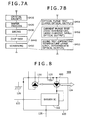
- Fig. 7 includes views illustrating a screening step of a semiconductor laser diode.
- Fig. 8 is a functional block diagram of an optical transmission module.
- the screening has been performed only using a test of high temperature and large current (hereinafter referred to as a current purge test), similarly to the semiconductor lasers using the active layer material of InGaAsP and the like with less crystal defects.
- the current purge test has been performed at 100 °C and 150 mA, so that the optical output itself has been small. Further, depending on circumstances, the screening test has often been performed under the condition that light is hardly emitted. In order to screen the initial failure due to the failure mode described above with reference to Fig. 2, it is necessary to perform a test at room temperature (25 °C) and large current (150 mA) (hereinafter referred to as an optical purge test).
- the abscissa represents the optical output
- the ordinate represents the degradation time indicated by the logarithmic scale.
- the failure product distribution of the products applied to the current purge test which is shown in Fig. 4, is a life test result of the working sample for semiconductor laser diode having been subjected to only the current purge test, in which the degradation time is about 20, 000.
- the semiconductor laser diode since the current purge test itself has been performed at an optical output ranging from 1 mW or less to several mW, the semiconductor laser diode generates an initial failure without being screened.
- the degradation time was evaluated with an optical output swing at 25 °C.
- the results are represented by five points indicated by black circles in Fig. 4.
- the screening conditions were defined by the solid line with a margin relative to the regression line (the dotted line in the figure) obtained from the five points. In other words, it is possible to assure a life of 10 mW 100,000 hours, by adding an optical purge test at 25 °C with 20 mW for 5 minutes into the screening step.
- a buffer layer 101 (n-type InP, 2E18 cm ⁇ -3, 0.4 ⁇ m) , an optical guide layer 102 (n-type InGaAlAs layer, 2E18 cm ⁇ -3, 0.1 ⁇ m), a multiple quantum well active layer 103 (well/barrier of InGaAlAs: 6 cycles, thickness 0.18 ⁇ m), an optical guide layer 104 (p-type InGaAlAs, 4E17 cm ⁇ -3, 0.03 ⁇ m), an InAlAs clad layer 105 (p-type InAlAs, 8E17 cm ⁇ -3, 0.06 ⁇ m), an etch stopper layer 106 (p-type InGaAsAs, 8E17 cm ⁇ -3, 0.05 ⁇ m), a spacer layer 107 (p-type InP, 8E17 cm ⁇ -3, 0.02 ⁇ m), and a grating layer 108 (p-type InGaAsP, 8E17 cm ⁇ -3, 0.02 ⁇ m), and a
- an InP clad layer 109 (p-type InP, 1E18 cm ⁇ -3, 1.3 ⁇ m) and a contact layer 110 (p-type InGaAs, 1E19 cm ⁇ -3, 0.2 ⁇ m) were crystal grown to form a ridge waveguide 114.
- the width of the ridge waveguide of a ridge waveguide type DFB semiconductor laser diode 400 was set to a range of 1 to 2 ⁇ m.
- the element was manufactured through formation of a passivation layer 117 (SiO2 film, 0.4 ⁇ m), formation of a p electrode 112 (Ti/Pt/Au, thickness 0.7 ⁇ m), bottomgrinding, formation of an n electrode 113 (AuGe/Ni/TiPt/Au, thickness 0.8 ⁇ m), and cleavage process.
- a non-reflective film was formed on a front end surface of the element, and a high reflective film was formed on a back end surface thereof.
- the length of a resonator was set to a range of 150 to 250 ⁇ m.
- a screening step shown in Fig. 7B was applied for eliminating the initial failure mode of the semiconductor laser diode 400 and of assuring the expected life needed for the communication laser.
- the manufacturing process of the semiconductor laser diode includes the following steps: crystal growth (S410), wafer process (S420), dicing (S430), chip test (S440), and screening (S450).
- an optical purge test 25 °C, initial optical output 23 mW: constant operation current, 3 minutes
- a current purge test 100 °C, current 100 mA: constant operating current, 20 hours
- an aging test 85 °C, initial operating current 80 mA: constant optical output, 100 hours
- the optical purge test was performed at constant operating current with the initial optical output of 23 mW, but it may be performed at constant optical output. Further, the optical output in the optical purge test may be not less than 15 mW, the value being equivalent to 50% of the saturation optical output, and more preferably not less than 20 mW.
- the same effect was obtained when ridge waveguide semiconductor laser diodes for a wavelength of 1. 55 ⁇ m band were manufactured, when Fabry-Perot type ridge waveguide semiconductor laser diodes were manufactured, when ridge waveguide semiconductor laser diodes were manufactured on p-type InP substrates, and when ridge waveguide semiconductor laser diodes using GaInNAs or AlGaAs as an active layer material were manufactured on GaAs substrates.
- the semiconductor lasers have the same effect when the materials, whose reliability is easily affected by crystal defects than the case of using InGaAsP as the active layer of the semiconductor laser, are applied as the active layers.
- the semiconductor laser diode 400 is provided in a case 120 placed in an optical transmission module 500, and is directly modulated and driven by a driver IC 122.
- the front optical signal of the semiconductor laser diode 400 is transmitted by an optical fiber not shown.
- the back light of the semiconductor laser diode 400 is monitored by a monitor photodiode 130.
- a thermistor is provided in the vicinity of the semiconductor laser diode 400 in the case 120 to monitor the temperature of the semiconductor laser diode 400.
- the back optical power and the temperature are used for a drive control of the semiconductor laser diode 400.
- the semiconductor laser diode 400 mounted on the optical transmission module 500 has been subjected to the optical purge test, so that there is no initial failure mode caused by the laser diode of the optical transmission module, thus making it possible to supply the module that is very stable in reliability and mass production into the market.
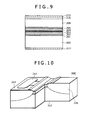
- Fig. 9 is a cross-sectional view of a semiconductor laser in an optical axis direction.
- Fig. 10 is a perspective partial cross-sectional view of the semiconductor laser in an optical axis direction.
- a buffer layer 201 (n-type InP, 1.5E18 cm ⁇ -3, 0.5 ⁇ m), an optical guide layer 202 (n-type InGaAlAs layer, 2E18 cm ⁇ -3, 0.1 ⁇ m), a multiple quantum well active layer 203 (well/barrier of InGaAlAs: 7 cycles, thickness 0.21 ⁇ m), an optical guide layer 204 (p-type InGaAlAs, 3E17 cm ⁇ -3, 0.1 ⁇ m), an InAlAs clad layer 205 (p-type InAlAs, 8E17 cm ⁇ -3, 0.1 ⁇ m), an InP clad layer 209 (p-type InP, 1E18 cm ⁇ -3, 1.4 ⁇ m), and a contact layer 210 (p-type InGaAs, 1E19 cm ⁇ -3, 0.15 ⁇ m) were crystal grown sequentially on an InP substrate 200 (n-type, 1.
- a waveguide is formed by etching through the multiple quantum well active layer.
- the width of the waveguide was set to a range of 1.2 to 2.3 ⁇ m.
- a buried-heterostructure laser diode was manufactured through formation of an Fe-InP regrowth layer 215 with high resistance, formation of a passivation film 217 (SiO2 film, 0.4 ⁇ m), formation of a p electrode 212 (Ti/Pt/Au, thickness 0. 7 ⁇ m), bottomgrinding, formation of an n electrode 213 (AuGe/Ni/TiPt/Au, thickness 0.8 ⁇ m), and cleavage process.
- a non-reflective film was formed on a front end surface of the buried-heterostructure laser diode 600, and a high reflective film was formed on a back end surface thereof.
- the length of a resonator of the buried-heterostructure laser diode 600 was set to a range of 150 to 250 ⁇ m.
- the screening step shown in Fig. 7B was applied for eliminating the initial failure mode of the semiconductor laser diode and of assuring the expected life needed for the communication laser.
- an optical purge test 50 °C, initial optical output 28 mW: constant operating current, 5 minutes
- a current purge test 110 °C, current 100 mA: constant operating current, 20 hours
- an aging test 85 °C, initial operating current 80 mA: constant optical output, 100 hours
- Fig. 11 is a cross-sectional view of a surface emitting semiconductor laser.
- Fig. 12 is a perspective partial cross-sectional view of the surface emitting semiconductor laser in an optical axis direction.
- a buffer layer 302 (n-type InP layer, 1E18 cm ⁇ -3, 0.2 ⁇ m), a semiconductor reflection mirror 303 (n-type InAlAs/InGaAlAs layer, 1E18 cm ⁇ -3, 42-cycle structure of ⁇ /4 film thickness each), a lower contact layer 352 (n-type InP layer, 5E17 cm ⁇ -3, 0.2 ⁇ m), a clad layer 353 (n-type InAlAs layer, 5E17 cm ⁇ -3, 0.2 ⁇ m), an MQW layer 354 (well/barrier of InGaAlAs: 7 cycles, thickness 0.2 ⁇ m), a clad layer 355 (p-type InAlAs layer, 5E17 cm ⁇ -3, 0.7 ⁇ m), and a tunnel junction layer 356 (p+-InGaAlAs/n+InGaAs layer, 3E19 cm ⁇ -3, 20 nm/12 nm) were crystal grown sequentially on an InP
- n-InP regrowth layer 360 n-type, thickness 0.1 ⁇ m
- upper contact layer 361 n-type InGaAs layer, 2E19 cm ⁇ -3, 0.1 ⁇ m
- the impurity concentration was reduced to 5E17 cm ⁇ -3 from the start of growth to when the thickness was 10 nm, and subsequently the impurity concentration was set to 5E18 cm ⁇ -3 until the thickness was 0.1 ⁇ m.
- portions of the upper contact layer 361 (InGaAs layer), which correspond to the portion directly on the current confinement region and to the surrounding area, were selectively etched and removed by wet etching, on which a dielectric multilayer film mirror 362 (AlxOy/a-Si, 4-cycle structure of ⁇ /4 film thickness each) was formed.
- the outside of a ring electrode 363 was designed to have a two-step mesa structure in order to reduce leakage current and capacity.
- a first mesa 331 was formed by etching from the InGaAs upper contact layer 361 to the clad layer 353.
- the surrounding of the first mesa 331 was embedded by a high-resistance InP regrowth layer 370 (thickness 0.6 ⁇ m).
- a second mesa 332 was formed by further etching the outside of the high-resistance InP regrowth layer 370 to the InP lower contact layer 352.
- an SiN film (0. 25 ⁇ m) was formed as a protective film 311.
- An upper ohmic electrode 371 (AuGe/Ni/TiPt/Au, thickness 0.7 ⁇ m) was brought into contact with the semiconductor in the upper contact layer 361 and the ring electrode 363.
- a wiring 314 (width 5 ⁇ m, length 100 ⁇ m) and an electrode pad 315 (75 ⁇ m ⁇ ) were provided on the SiN film 311 and the InP regrowth layer 370. In this way the configuration was designed to reduce the parasitic capacitance and to prevent the occurrence of the breaking of the wiring.
- a lower ohmic electrode 372 (AuGe/Ni/Ti/Pt/Au, thickness 0.7 ⁇ m) was formed on the top simultaneously with the formation of the upper ohmic electrode 371.
- the bottom of the InP substrate 301 in which no active region of the element was provided was ground to a thickness of 100 ⁇ m, and then a bottom metal film 317 for die bonding (AuGe/Ni/Ti/Pt/Au, thickness 0.8 ⁇ m) was provided on the bottom.
- a surface emitting semiconductor laser diode 700 shown in Fig. 12 was formed.
- the screening step shown in Fig. 7B was applied for eliminating the initial failure mode of the above described surface emitting semiconductor laser diode, and assuring the expected life needed for the communication laser.
- an optical purge test (10 °C, initial optical output 2 mW: constant operating current, 10 minutes) was performed (S451).
- a current purge test (100 °C, current 10 mA: constant operating current, 20 hours) was further performed (S452) .
- an aging test 85 °C, initial operating current 4 mA: constant optical output, 100 hours
- no degradation was observed in any of the elements input to the test.
- the optical output is about one tenth and the drive current is also about one tenth, as compared to the case of the side emitting laser diode.
- the initial optical output (2 mW) of the optical purge test of the surface emitting laser diode is 50% or more of the saturation optical output value, which is equivalent to the case of the side emitting laser diode.
- the present invention has made it possible to establish the screening conditions of a communication laser using a material with relatively many crystal defects for the active material. It has alsomade it possible toprovide a communication laser with high reliability.
Landscapes
- Physics & Mathematics (AREA)
- Optics & Photonics (AREA)
- Condensed Matter Physics & Semiconductors (AREA)
- General Physics & Mathematics (AREA)
- Electromagnetism (AREA)
- Engineering & Computer Science (AREA)
- Nanotechnology (AREA)
- Chemical & Material Sciences (AREA)
- Biophysics (AREA)
- Crystallography & Structural Chemistry (AREA)
- Life Sciences & Earth Sciences (AREA)
- Semiconductor Lasers (AREA)
- Testing Of Individual Semiconductor Devices (AREA)
- Led Devices (AREA)
Applications Claiming Priority (1)
| Application Number | Priority Date | Filing Date | Title |
|---|---|---|---|
| JP2006225153A JP2008053268A (ja) | 2006-08-22 | 2006-08-22 | 通信用半導体レーザの製造方法、通信用半導体レーザおよび光送信モジュール |
Publications (2)
| Publication Number | Publication Date |
|---|---|
| EP1919044A2 true EP1919044A2 (de) | 2008-05-07 |
| EP1919044A3 EP1919044A3 (de) | 2009-10-07 |
Family
ID=39129270
Family Applications (1)
| Application Number | Title | Priority Date | Filing Date |
|---|---|---|---|
| EP07014544A Withdrawn EP1919044A3 (de) | 2006-08-22 | 2007-07-24 | Verfahren zur Herstellung von Halbleiterlasern zur Kommunikation, Halbleiterlaser zur Kommunikation und optische Übertragungsmodule |
Country Status (5)
| Country | Link |
|---|---|
| US (1) | US7833807B2 (de) |
| EP (1) | EP1919044A3 (de) |
| JP (1) | JP2008053268A (de) |
| KR (1) | KR20080018098A (de) |
| CN (1) | CN101132112B (de) |
Families Citing this family (9)
| Publication number | Priority date | Publication date | Assignee | Title |
|---|---|---|---|---|
| JP2009239260A (ja) * | 2008-03-07 | 2009-10-15 | Mitsubishi Electric Corp | 半導体レーザおよびその製造方法 |
| JP2009238857A (ja) * | 2008-03-26 | 2009-10-15 | Opnext Japan Inc | 半導体レーザのスクリーニング方法および製造方法 |
| JP5056549B2 (ja) * | 2008-04-04 | 2012-10-24 | 日亜化学工業株式会社 | 光半導体素子の寿命予測方法および光半導体素子の駆動装置 |
| US7795896B2 (en) * | 2008-08-13 | 2010-09-14 | Finisar Corporation | High-power optical burn-in |
| US9488779B2 (en) * | 2013-11-11 | 2016-11-08 | Taiwan Semiconductor Manufacturing Company, Ltd. | Apparatus and method of forming laser chip package with waveguide for light coupling |
| JP7379334B2 (ja) * | 2018-07-27 | 2023-11-14 | ヌヴォトンテクノロジージャパン株式会社 | 半導体レーザ素子、検査方法及び検査装置 |
| CN111585164B (zh) * | 2020-05-14 | 2021-07-06 | 苏州长瑞光电有限公司 | 一种垂直腔面发射激光器快速老化方法及装置 |
| US20230208108A1 (en) * | 2021-12-23 | 2023-06-29 | Ii-Vi Delaware, Inc. | Semiconductor laser diode including inverted p-n junction |
| JP2023132201A (ja) * | 2022-03-10 | 2023-09-22 | 株式会社Hrd | 電磁波を出射する半導体素子の劣化抑制方法 |
Family Cites Families (10)
| Publication number | Priority date | Publication date | Assignee | Title |
|---|---|---|---|---|
| US4573255A (en) * | 1984-03-22 | 1986-03-04 | At&T Bell Laboratories | Purging: a reliability assurance technique for semiconductor lasers utilizing a purging process |
| JP2976812B2 (ja) * | 1993-07-13 | 1999-11-10 | 住友電気工業株式会社 | 半導体レーザの選別方法 |
| JP2630264B2 (ja) * | 1994-03-24 | 1997-07-16 | 日本電気株式会社 | 歪量子井戸半導体レーザ |
| JPH10303496A (ja) | 1997-04-30 | 1998-11-13 | Fujitsu Ltd | 半導体レーザのスクリーニング方法 |
| DE69902412T2 (de) * | 1998-02-04 | 2003-04-10 | Mitsui Chemicals, Inc. | Oberflächenemittierender Laser |
| JP3923192B2 (ja) * | 1998-09-02 | 2007-05-30 | 三菱電機株式会社 | 半導体レーザ素子のスクリーニング方法 |
| EP1195864A3 (de) * | 2000-10-04 | 2004-11-10 | Matsushita Electric Industrial Co., Ltd. | Halbleiterlaservorrichtung |
| JP2002289977A (ja) * | 2001-03-26 | 2002-10-04 | Ricoh Co Ltd | 半導体素子の製造方法および半導体素子および光送信モジュールおよび光送受信モジュールおよび光通信システム |
| JP2003014990A (ja) * | 2001-06-29 | 2003-01-15 | Sumitomo Electric Ind Ltd | 光通信モジュール |
| JP4677922B2 (ja) * | 2006-02-15 | 2011-04-27 | 住友電気工業株式会社 | 半導体レーザ素子の検査方法 |
-
2006
- 2006-08-22 JP JP2006225153A patent/JP2008053268A/ja active Pending
-
2007
- 2007-07-24 EP EP07014544A patent/EP1919044A3/de not_active Withdrawn
- 2007-08-01 CN CN2007101398088A patent/CN101132112B/zh active Active
- 2007-08-02 US US11/882,595 patent/US7833807B2/en active Active
- 2007-08-02 KR KR1020070077883A patent/KR20080018098A/ko not_active Ceased
Non-Patent Citations (1)
| Title |
|---|
| None |
Also Published As
| Publication number | Publication date |
|---|---|
| CN101132112B (zh) | 2011-04-20 |
| JP2008053268A (ja) | 2008-03-06 |
| EP1919044A3 (de) | 2009-10-07 |
| CN101132112A (zh) | 2008-02-27 |
| US7833807B2 (en) | 2010-11-16 |
| US20080089378A1 (en) | 2008-04-17 |
| KR20080018098A (ko) | 2008-02-27 |
Similar Documents
| Publication | Publication Date | Title |
|---|---|---|
| US7833807B2 (en) | Method of manufacturing semiconductor laser for communication, semiconductor laser for communication and optical transmission module | |
| US7260130B2 (en) | Semiconductor laser device and method of fabricating the same | |
| US8300671B2 (en) | Surface emitting laser | |
| US20080013581A1 (en) | Low optical feedback noise self-pulsating semiconductor laser | |
| US6810065B1 (en) | Low electrical resistance n-type mirror for optoelectronic devices | |
| US7760782B2 (en) | Distributed bragg reflector type directly modulated laser and distributed feed back type directly modulated laser | |
| EP0560358B1 (de) | Lasersystem | |
| US9157949B2 (en) | Accelerating the aging of multiple lasers | |
| JP2009238857A (ja) | 半導体レーザのスクリーニング方法および製造方法 | |
| US20040233954A1 (en) | Surface-emitting semiconductor laser element having selective-oxidation type or ion-injection type current-confinement structure, InGaAsp quantum well, and InGaP or InGaAsp barrier layers | |
| Gao et al. | High-power highly reliable single emitter laser diodes at 808 nm | |
| JP4431008B2 (ja) | 半導体レーザの熱抵抗評価装置および熱抵抗評価方法 | |
| JP2011171759A (ja) | 通信用半導体レーザの製造方法および通信用半導体レーザ | |
| Yan et al. | Bonding stress and reliability of low-polarization quantum-well superluminescent diode | |
| Okuda et al. | Low-Operation-Current and Highly-Reliable 1.3-µm AlGaInAs Strain Compensated MQW-BH-DFB Lasers for 100° C, 10-Gb/s Operation | |
| Han et al. | Wafer level reliability and lifetime analysis of InGaAsP/InP quantum-well Fabry-Pérot laser diode | |
| Xu et al. | Highly reliable, high-brightness 915nm laser diodes for fiber laser applications | |
| EP1104054B1 (de) | Halbleiterlaser | |
| JP2003174226A (ja) | 半導体レーザ素子、それを用いたレーザモジュール | |
| Goodwin et al. | Reliability considerations of multi-quantum-well sources for optical fiber communication systems | |
| Green et al. | Horizontal cavity vertically emitting lasers with integrated monitor photodiodes | |
| Lee et al. | High-Reliable and High-Speed 1.3$\mu $ m Complex-Coupled Distributed Feedback Buried-Heterostructure Laser Diodes With Fe-Doped InGaAsP/InP Hybrid Grating Layers Grown by MOCVD | |
| Ikegami et al. | Optoelectronics reliability | |
| Resneau et al. | Long-term aging with highly stable performances of 1.55-µm DFB lasers for microwave optical links | |
| Hepburn et al. | GaInNAs and GaAs, top‐hat vertical‐cavity semiconductor optical amplifier (VCSOA) based on longitudinal current transport |
Legal Events
| Date | Code | Title | Description |
|---|---|---|---|
| PUAI | Public reference made under article 153(3) epc to a published international application that has entered the european phase |
Free format text: ORIGINAL CODE: 0009012 |
|
| AK | Designated contracting states |
Kind code of ref document: A2 Designated state(s): AT BE BG CH CY CZ DE DK EE ES FI FR GB GR HU IE IS IT LI LT LU LV MC MT NL PL PT RO SE SI SK TR |
|
| AX | Request for extension of the european patent |
Extension state: AL BA HR MK RS |
|
| 17P | Request for examination filed |
Effective date: 20080331 |
|
| PUAL | Search report despatched |
Free format text: ORIGINAL CODE: 0009013 |
|
| AK | Designated contracting states |
Kind code of ref document: A3 Designated state(s): AT BE BG CH CY CZ DE DK EE ES FI FR GB GR HU IE IS IT LI LT LU LV MC MT NL PL PT RO SE SI SK TR |
|
| AX | Request for extension of the european patent |
Extension state: AL BA HR MK RS |
|
| AKX | Designation fees paid |
Designated state(s): DE FR GB |
|
| RAP1 | Party data changed (applicant data changed or rights of an application transferred) |
Owner name: OCLARO JAPAN, INC. |
|
| RAP1 | Party data changed (applicant data changed or rights of an application transferred) |
Owner name: OCLARO JAPAN, INC. |
|
| 17Q | First examination report despatched |
Effective date: 20151014 |
|
| STAA | Information on the status of an ep patent application or granted ep patent |
Free format text: STATUS: THE APPLICATION IS DEEMED TO BE WITHDRAWN |
|
| 18D | Application deemed to be withdrawn |
Effective date: 20160225 |