EP1918776A1 - Etching of nano-imprint templates using an etch reactor - Google Patents
Etching of nano-imprint templates using an etch reactor Download PDFInfo
- Publication number
- EP1918776A1 EP1918776A1 EP07020929A EP07020929A EP1918776A1 EP 1918776 A1 EP1918776 A1 EP 1918776A1 EP 07020929 A EP07020929 A EP 07020929A EP 07020929 A EP07020929 A EP 07020929A EP 1918776 A1 EP1918776 A1 EP 1918776A1
- Authority
- EP
- European Patent Office
- Prior art keywords
- etching
- resist material
- containing gas
- layer
- gas
- Prior art date
- Legal status (The legal status is an assumption and is not a legal conclusion. Google has not performed a legal analysis and makes no representation as to the accuracy of the status listed.)
- Granted
Links
Images


Classifications
-
- H—ELECTRICITY
- H10—SEMICONDUCTOR DEVICES; ELECTRIC SOLID-STATE DEVICES NOT OTHERWISE PROVIDED FOR
- H10P—GENERIC PROCESSES OR APPARATUS FOR THE MANUFACTURE OR TREATMENT OF DEVICES COVERED BY CLASS H10
- H10P76/00—Manufacture or treatment of masks on semiconductor bodies, e.g. by lithography or photolithography
- H10P76/20—Manufacture or treatment of masks on semiconductor bodies, e.g. by lithography or photolithography of masks comprising organic materials
- H10P76/204—Manufacture or treatment of masks on semiconductor bodies, e.g. by lithography or photolithography of masks comprising organic materials of organic photoresist masks
- H10P76/2041—Photolithographic processes
-
- B—PERFORMING OPERATIONS; TRANSPORTING
- B82—NANOTECHNOLOGY
- B82Y—SPECIFIC USES OR APPLICATIONS OF NANOSTRUCTURES; MEASUREMENT OR ANALYSIS OF NANOSTRUCTURES; MANUFACTURE OR TREATMENT OF NANOSTRUCTURES
- B82Y10/00—Nanotechnology for information processing, storage or transmission, e.g. quantum computing or single electron logic
-
- B—PERFORMING OPERATIONS; TRANSPORTING
- B82—NANOTECHNOLOGY
- B82Y—SPECIFIC USES OR APPLICATIONS OF NANOSTRUCTURES; MEASUREMENT OR ANALYSIS OF NANOSTRUCTURES; MANUFACTURE OR TREATMENT OF NANOSTRUCTURES
- B82Y40/00—Manufacture or treatment of nanostructures
-
- C—CHEMISTRY; METALLURGY
- C23—COATING METALLIC MATERIAL; COATING MATERIAL WITH METALLIC MATERIAL; CHEMICAL SURFACE TREATMENT; DIFFUSION TREATMENT OF METALLIC MATERIAL; COATING BY VACUUM EVAPORATION, BY SPUTTERING, BY ION IMPLANTATION OR BY CHEMICAL VAPOUR DEPOSITION, IN GENERAL; INHIBITING CORROSION OF METALLIC MATERIAL OR INCRUSTATION IN GENERAL
- C23F—NON-MECHANICAL REMOVAL OF METALLIC MATERIAL FROM SURFACE; INHIBITING CORROSION OF METALLIC MATERIAL OR INCRUSTATION IN GENERAL; MULTI-STEP PROCESSES FOR SURFACE TREATMENT OF METALLIC MATERIAL INVOLVING AT LEAST ONE PROCESS PROVIDED FOR IN CLASS C23 AND AT LEAST ONE PROCESS COVERED BY SUBCLASS C21D OR C22F OR CLASS C25
- C23F4/00—Processes for removing metallic material from surfaces, not provided for in group C23F1/00 or C23F3/00
-
- G—PHYSICS
- G03—PHOTOGRAPHY; CINEMATOGRAPHY; ANALOGOUS TECHNIQUES USING WAVES OTHER THAN OPTICAL WAVES; ELECTROGRAPHY; HOLOGRAPHY
- G03F—PHOTOMECHANICAL PRODUCTION OF TEXTURED OR PATTERNED SURFACES, e.g. FOR PRINTING, FOR PROCESSING OF SEMICONDUCTOR DEVICES; MATERIALS THEREFOR; ORIGINALS THEREFOR; APPARATUS SPECIALLY ADAPTED THEREFOR
- G03F1/00—Originals for photomechanical production of textured or patterned surfaces, e.g., masks, photo-masks, reticles; Mask blanks or pellicles therefor; Containers specially adapted therefor; Preparation thereof
- G03F1/68—Preparation processes not covered by groups G03F1/20 - G03F1/50
-
- G—PHYSICS
- G03—PHOTOGRAPHY; CINEMATOGRAPHY; ANALOGOUS TECHNIQUES USING WAVES OTHER THAN OPTICAL WAVES; ELECTROGRAPHY; HOLOGRAPHY
- G03F—PHOTOMECHANICAL PRODUCTION OF TEXTURED OR PATTERNED SURFACES, e.g. FOR PRINTING, FOR PROCESSING OF SEMICONDUCTOR DEVICES; MATERIALS THEREFOR; ORIGINALS THEREFOR; APPARATUS SPECIALLY ADAPTED THEREFOR
- G03F1/00—Originals for photomechanical production of textured or patterned surfaces, e.g., masks, photo-masks, reticles; Mask blanks or pellicles therefor; Containers specially adapted therefor; Preparation thereof
- G03F1/68—Preparation processes not covered by groups G03F1/20 - G03F1/50
- G03F1/80—Etching
-
- G—PHYSICS
- G03—PHOTOGRAPHY; CINEMATOGRAPHY; ANALOGOUS TECHNIQUES USING WAVES OTHER THAN OPTICAL WAVES; ELECTROGRAPHY; HOLOGRAPHY
- G03F—PHOTOMECHANICAL PRODUCTION OF TEXTURED OR PATTERNED SURFACES, e.g. FOR PRINTING, FOR PROCESSING OF SEMICONDUCTOR DEVICES; MATERIALS THEREFOR; ORIGINALS THEREFOR; APPARATUS SPECIALLY ADAPTED THEREFOR
- G03F7/00—Photomechanical, e.g. photolithographic, production of textured or patterned surfaces, e.g. printing surfaces; Materials therefor, e.g. comprising photoresists; Apparatus specially adapted therefor
- G03F7/0002—Lithographic processes using patterning methods other than those involving the exposure to radiation, e.g. by stamping
Definitions
- Embodiments of the present invention relate to the fabrication of structures using nano-imprint technology, particularly, to methods of etching metal layers using an imprinted resist material, and more particularly to methods for processing a photolithographic reticle,
- Nano-imprint technology is utilized for the fabrication of micro- and nano-structures.
- Nano-imprint is a mechanical replication technology wherein a mold is pressed into a UV curable resist that was spin-coated on a substrate. UV irradiation of the resist through the mold in the imprinted area leads to the polymerization and curing of the resist. The mold is then removed leaving the inverted three dimensional replica of the pattern formed in the resist. The thin portions of the imprinted resist are removed to create openings in the resist layer, forming a mask that is then utilized to etch one or more layers underlying the resist. This technique enables fast high precision printing down to 10nm spacing and pattern fidelity to a large extent.
- Plasma etch processing known as dry etch processing or dry etching
- dry etch processing provides a more anisotropic etch than wet etching processes.
- the dry etching process has been shown to produce less undercutting and to improve the retention of the critical dimensions of the photomask features formed using conventional lithographic techniques with straighter sidewalls and flatter bottoms.
- dry etching may overetch or imprecisely etch the sidewalls of the openings or pattern formed in the resist material used to define the critical dimensions of the underlying layer. Excess side removal of the resist material results in a loss of the critical dimensions of the patterned resist features, which may translate to a loss of critical dimensions of the features formed in the underlying layer defined by the patterned resist.
- imprecise etching may not sufficiently etch the features to provide the necessary critical dimensions. Failure to sufficiently etch the features to the critical dimensions is referred to as a "gain" of critical dimensions. The degree of loss or gain of the critical dimensions in the metal layer is referred to as "etching bias" or "CD bias”.
- loss of critical dimension control is of concern in most all etching applications, it is particularly problematic in photomask fabrication.
- the loss or gain of critical dimensions of the pattern formed in the underlying layer(s) comprising a photomask reticle can detrimentally affect the light passing therethrough and produce numerous patterning defects and subsequent etching defects in substrates patterned by the photolithographic reticle.
- the loss or gain of critical dimensions of the photomask can result in insufficient photolithographic performance for etching high aspect ratios of sub-micron features and, if the loss or gain of critical dimensions is severe enough, the failure of the photolithographic reticle or subsequently etched device. Since nano-imprint technology can produce very small apertures, conventional etching techniques do not allow effective pattern transfer to the layers underlying the imprinted resist to a degree acceptable for robust photomask fabrication.
- a method for processing a photolithographic reticle that includes providing a reticle having a metal photomask layer formed on an optically transparent substrate and an imprinted resist material deposited on the metal photomask layer, etching recessed regions of the imprinted resist material to expose portions of the metal photomask layer in a first etching step, and etching the exposed portions of the metal photomask layer through the imprinted resist material in a second etching step, wherein at least one of the first or second etching steps utilizes a plasma formed from a processing gas comprising an oxygen containing gas, a chlorine containing gas and a halogen containing gas.
- the process gas is utilized in both the first and second etching steps includes an oxygen containing gas, a chlorine containing gas and a halogen containing gas.
- the process gas is utilized in both the first and second etching steps have different ratios of oxygen containing gas, chlorine containing gas and halogen containing gas.
- the first and second etching steps are performed in the same processing chamber.
- Embodiments are also directed to apparatuses for carrying out the disclosed methods and including apparatus parts for performing described method steps.
- embodiments are also directed to methods by which the described apparatus is manufactured. It may include method steps for manufacturing parts of the apparatus. The method steps may be performed by way of hardware components, firmware, software, a computer programmed by appropriate software, by any combination thereof or in any other manner.
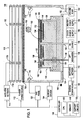
- Figure 1 is a schematic cross-sectional view of one embodiment of an etching chamber
- Figure 2 is a flow chart illustrating one embodiment of a sequence for processing a substrate according to one embodiment of the invention.
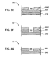
- Figures 3A-3G are cross-sectional views showing an etching sequence of another embodiment of the invention.
- Suitable inductively coupled plasma etch chambers include the TetraTM family of photomask etch chambers, or optionally, a Decoupled Plasma Source (DPS ITM, DPS IITM, and DPS PlusTM) processing chambers, all available from Applied Materials, Inc., of Santa Clara, California.
- DPS ITM, DPS IITM, and DPS PlusTM Decoupled Plasma Source
- Process chambers may be used to perform the processes of the invention, including, for example, capacitively coupled parallel plate chambers and magnetically enhanced ion etch chambers as well as inductively coupled plasma etch chambers of different designs. Examples of such suitable processing chambers are disclosed in U.S. Patent Application Serial No. 09/325,026, filed on June 3, 1999 , U.S. Patent Application Serial No. 11/554,502, filed on October 30, 2006 , and in U.S. Patent Application Serial No. 11/554,495, filed on October 30, 2006 . Although the processes are advantageously performed with the TetraTM photomask etch chamber, the description of the processing chamber is illustrative, and should not be construed or interpreted to limit the scope of any aspect of the invention. It is also contemplated that the invention may be beneficially practiced in other processing chambers, including those from other manufacturers.
- FIG 1 is a schematic cross-sectional view of one embodiment of a processing chamber 100 generally comprising a process chamber body 102 having a substrate pedestal 124, and a controller 146.
- the chamber body 102 has a conductive wall 104 that supports a substantially flat dielectric ceiling 108.
- Other embodiments of the processing chamber 100 may have other types of ceilings, e.g., a dome-shaped ceiling.
- An antenna 110 is disposed above the ceiling 108.
- the antenna 110 comprises one or more inductive coil elements that may be selectively controlled (two co-axial elements 110a and 110b are shown in Figure 1).
- the antenna 110 is coupled through a first matching network 114 to a plasma power source 112.
- the plasma power source 112 is typically capable of producing up to about 3000 Watts (W) at a tunable frequency in a range from about 50 kHz to about 13.56 MHz.
- the substrate pedestal (cathode) 124 is coupled through a second matching network 142 to a biasing power source 140.
- the biasing source 140 provides between about zero to about 600 W at a tunable pulse frequency in the range of about 1 to about 10 kHz.
- the biasing source 140 produces pulsed RF power output.
- the biasing source 140 may produce pulsed DC power output. It is contemplated that the source 140 may also provide a constant DC and/or RF power output.
- the substrate support pedestal 124 includes an electrostatic chuck 160.
- the electrostatic chuck 160 comprises at least one clamping electrode 132 and is controlled by a chuck power supply 166.
- the substrate pedestal 124 may comprise substrate retention mechanisms such as a susceptor clamp ring, a vacuum chuck, a mechanical chuck, and the like.
- a gas panel 120 is coupled to the processing chamber 100 to provide process and/or other gases to the interior of the process chamber body 102.
- the gas panel 120 is coupled to one or more inlets 116 formed in a channel 118 in the sidewall 104 of the chamber body 102. It is contemplated that the one or more inlets 116 may be provided in other locations, for example, in the ceiling 108 of the processing chamber 100.
- the pressure in the processing chamber 100 is controlled using a throttle valve 162 and a vacuum pump 164.
- the vacuum pump 164 and throttle valve 162 are capable of maintaining chamber pressures in the range of about 1 to about 20 mTorr.
- the temperature of the wall 104 may be controlled using liquid-containing conduits (not shown) that run through the wall 104. Wall temperature is generally maintained at about 65 degrees Celsius.
- the chamber wall 104 is formed from a metal (e.g., aluminum, stainless steel, and the like) and is coupled to an electrical ground 106.
- the processing chamber 100 also comprises conventional systems for process control, internal diagnostic, end point detection, and the like. Such systems are collectively shown as support systems 154.
- a reticle adapter 182 is used to secure a substrate (such as a reticle or other workpiece) 122 onto the substrate support pedestal 124.
- the reticle adapter 182 generally includes a lower portion 184 milled to cover an upper surface of the pedestal 124 (for example, the electrostatic chuck 160) and a top portion 186 having an opening 188 that is sized and shaped to hold the substrate 122.
- the opening 188 is generally substantially centered with respect to the pedestal 124.
- the adapter 182 is generally formed from a single piece of etch resistant, high temperature resistant material such as polyimide ceramic or quartz.
- a suitable reticle adapter is disclosed in United States Patent No. 6,251,217, issued on June 26, 2001 .
- An edge ring 126 may cover and/or secure the adapter 182 to the pedestal 124.
- a lift mechanism 138 is used to lower or raise the adapter 182, and hence, the substrate 122, onto or off of the substrate support pedestal 124.
- the lift mechanism 138 comprises a plurality of lift pins (one lift pin 130 is shown) that travel through respective guide holes 136.
- the temperature of the substrate 122 is controlled by stabilizing the temperature of the substrate pedestal 124.
- the substrate support pedestal 124 comprises a heater 144 and an optional heat sink 128.
- the heater 144 may be one or more fluid conduits configured to flow a heat transfer fluid therethrough.
- the heater 144 may include at least one heating element 134 that is regulated by a heater power supply 168.
- a backside gas e.g., helium (He)
- He helium
- the backside gas is used to facilitate heat transfer between the pedestal 124 and the substrate 122.
- the pedestal 124 may be heated by the embedded heater 144 to a steady-state temperature, which in combination with the helium backside gas, facilitates uniform heating of the substrate 122.
- the controller 146 comprises a central processing unit (CPU) 150, a memory 148, and support circuits 152 for the CPU 150 and facilitates control of the components of the processing chamber 100 and, as such, of the etch process, as discussed below in further detail.
- the controller 146 may be one of any form of general-purpose computer processor that can be used in an industrial setting for controlling various chambers and sub-processors.
- the memory 148 of the CPU 150 may be one or more of readily available memory such as random access memory (RAM), read only memory (ROM), floppy disk, hard disk, or any other form of digital storage, local or remote.
- the support circuits 152 are coupled to the CPU 150 for supporting the processor in a conventional manner.
- circuits include cache, power supplies, clock circuits, input/output circuitry and subsystems, and the like.
- the inventive method is generally stored in the memory 148 or other computer-readable medium accessible to the CPU 150 as a software routine.
- software routine may also be stored and/or executed by a second CPU (not shown) that is remotely located from the hardware being controlled by the CPU 150.
- the invention contemplates the use of processing parameters outside the ranges described herein for performing this process in different apparatus, such as a different etching chamber, and for different substrate sizes, such as photolithographic reticles for 200 mm and/or 300 mm substrate processing.
- etching metal layers such as chromium and chromium oxynitride
- the etching gases may be used to etch other material layers formed on substrates in semiconductor and photolithographic reticle manufacturing.
- a photolithographic reticle includes an opaque layer, known as a photomask, deposited on an optically transparent substrate.
- the opaque layer may comprise a metal layer, for example, chromium, or another material known or unknown in the art suitable for use as a photomask.
- the invention contemplates that the opaque layer may comprise a non-metallic dielectric material.
- An optically transparent material of the substrate 122 is broadly defined to include, but not limited to, a material transparent to light having wavelengths of about 300 nanometers (nm) or less, for example, transparent to ultraviolet light having wavelengths of 248 nm and 193 nm.
- Figure 2 is a flow chart of one embodiment of one process sequence of an etching process 200 suitable for etching a metal layer through an imprinted resist layer.
- the flow chart is provided for illustrative purposes and should not be construed as limiting the scope of any aspects of the invention.
- Figures 3A-3G illustrate the composition of the photolithographic reticle at points during the photomask forming process as well as further illustrate the process described above in Figure 2.
- the substrate 122 typically comprising an optically transparent material 310, such as optical quality quartz, fused silica material, molybdenum silicide (MoSi), molybdenum silicon oxynitride (MoSi x N y O z ), calcium fluoride, alumina, sapphire, or combinations thereof, is provided to a processing chamber at block 210, such as the processing chamber 100 of Figure 1.
- an optically transparent material 310 such as optical quality quartz, fused silica material, molybdenum silicide (MoSi), molybdenum silicon oxynitride (MoSi x N y O z ), calcium fluoride, alumina, sapphire, or combinations thereof.
- the substrate 122 has an opaque metal layer 320 as a metal photomask layer, typically comprising chromium, disposed on the substrate material 310, as shown in Figure 3A.
- the chromium layer may be deposited by conventional methods known in the art, such as by physical vapor deposition (PVD) or chemical vapor deposition (CVD) techniques.
- the metal layer 320 is typically deposited to a thickness between about 50 and about 100 nm; however, the thickness of the metal layer 320 may differ based upon the requirements of the manufacturer and the composition of the materials of the substrate or metal layer.
- an anti-reflective coating may be formed on or comprise part of the deposited metal layer 320.
- the ARC layer is believed to improve photolithographic precision in patterning features to be formed in the opaque layer.
- the ARC layer may be a metal layer incorporating nonmetallic contaminants or impurities to form, for example a metal oxynitride layer, such as chromium oxynitride. Chromium oxynitride may be formed during deposition of the metal layer or by exposing the metal layer to a suitable atmosphere, such as an oxidizing and nitrating environment.
- the chromium oxynitride layer may be deposited by conventional methods known in the art, such as by physical vapor deposition (PVD) or chemical vapor deposition (CVD) techniques.
- the metal oxynitride layer may comprise up to the top 25 percent of the total thickness of the metal layer 320.
- the optional ARC layer is typically formed at a thickness between about 10 nm and about 15 nm; however, the thickness of the layer may differ based upon the requirements of the manufacturer and the composition of the materials of the substrate or metal layer, and may be mainly concentrated in the upper surface of the deposited material, such as the upper 30 percent of the thickness of the original metal layer 320.
- the chromium oxynitride film is believed to be more sensitive to etching with oxygen radicals than chromium films. A reduced amount of oxygen in the processing gas may be used to effectively etch the chromium oxynitride surface compared to etching the bulk of the remaining chromium material.
- a resist layer 330A is deposited on the metal layer 320 at block 220.
- the resist layer material is usually low temperature resist material, which is defined herein as a polymeric material that thermally degrade at temperatures above about 250 degrees Celsius, an example of which includes "ZEP," manufactured by Hoya Corporation, among others.
- the resist layer 330A may be applied to the metal layer 320 via a spin-coating or other method.
- the resist material 330A may be deposited upon the metal layer 320 to a thickness between about 200 nm and about 600 nm, as shown in Figure 3B.
- the resist layer 330A is imprinted to form an imprinted resist layer 330B, as shown in the sequence depicted in Figures 3C-D.
- the resist layer 330A is contacted by a patterned surface 392 of a mold 390.
- the soft resist material of the layer 330A conforms to the patterned mold surface 392.
- the mold 390 is generally made of a material that is transmissive to energy that cures the resist material. Energy is provided to cure the resist material which remains in contact with the mold 390, such that when the mold 390 is removed, the pattern 392 leaves an inverse imprint 394 on the cured resist material to form the imprinted resist layer 330B.
- the imprint 394 generally includes a plurality of recessed surfaces 398 surrounded by a plurality of raised surfaces 396, as shown in Figure 3D.
- the recessed surfaces 398 may be coplanar (i.e., have a common depth relative to the raised surfaces 396) or may be parallel at different elevations.
- the substrate 122 is then transferred to an etch chamber, such as the processing chamber 100 described above, for forming the patterned resist mask and etching the metal layer 320 at block 240.
- an etch chamber such as the processing chamber 100 described above
- the openings or patterns in the metal layer 320 for formed by etching the imprinted resist layer 330B.
- Regions (later referred to as "pattern 325") of the imprinted resist layer 330B defined by the recessed surfaces 398 are etched through to expose portions the metal layer 320, thereby creating a patterned mask 330C from the imprinted resist layer 330B, as shown in Figure 3E.
- the imprinted resist layer 330B may be etched using any suitable chemistry, or with the same chemistry utilized to etch the metal layer 320 described below, for form an opening 335 having the dimension of the pattern 325. Utilizing the same chemistry to etch both the imprinted resist layer 330B and the metal layer 320 advantageously reduces the number of process gases need, along with simplifying chamber design. This provides both a cost and throughput advantage as extra gases, gas connections and purge cycles may be eliminated.
- the patterned mask 330C may be formed prior to placement in the processing chamber 100 by optically using a laser patterning device or by another radiative energy patterning device, such as an electron beam emitter to form the pattern 325 that is used to define the dimensions of the feature definition to be formed in the metal layer 320.
- a laser patterning device or by another radiative energy patterning device, such as an electron beam emitter to form the pattern 325 that is used to define the dimensions of the feature definition to be formed in the metal layer 320.
- the opaque, metal layer 320 then is etched in the processing chamber 100 at block 250.
- the patterns (i.e., dimensions of the pattern 325) are transferred to the metal layer 320 by etching the metal layer to expose the underlying optically transparent substrate material, and optionally, an ARC layer, as shown in Figure 3F, by extending the opening 335.
- Etching of exposed portions of the opaque metal layer 320 occurs by generating a plasma of a processing gas by supplying a source power and/or a bias power to the processing chamber 100.
- the processing gas for etching the metal layer 320 (and, in one embodiment, the imprinted resist layer 330B) generally includes an oxygen containing gas, a chlorine containing gas and a halogen containing gas. In one embodiment, no inert gases are included in the processing gas.
- the oxygen containing gas may include at least one of oxygen (O, O 2 , or O 3 ), carbon monoxide (CO), or carbon dioxide (CO 2 ), among others.
- the oxygen containing gas is oxygen is oxygen (O 2 ).
- the oxygen containing gas provides a source of etching radicals. Carbon monoxide (CO) and carbon dioxide (CO 2 ) gases, when selected, may provide a source of material for forming passivating polymer deposits, which may improve etch bias.
- the chlorine containing gas may include at least one of chlorine gas (Cl 2 ), carbon tetrachloride (CCl 4 ) or hydrogen chloride (HCl), among others.
- the chlorine containing gas is Cl 2 .
- the chlorine containing gas is used to supply highly reactive radicals to etch the metal layer.
- the chlorine containing gas provides a source of etching radicals and components, such as carbon tetrachloride (CCl 4 ) gas, that may provide a source of material for forming passivating polymer deposits, which may improve etch bias.
- the halogen containing gas may be at least one of hydrogen bromide (HBr), hydrogen iodide (Hl), trifluoromethane (CHF 3 ), sulfur hexafluoride (SF 6 ), hexafluoroethane (C 2 F 6 ) or ammonia (NH 3 ), among others.
- the halogen containing gas may be selected to increase the etch selectivity of chromium to photoresist, and reduce etch bias.
- the halogen containing gas is hydrogen bromide (HBr).
- Hydrogen bromide may also be delivered to processing from an aqueous solution or have an aqueous component as hydrobromic acid.
- the halogen containing gas may be used to supply both reactive radicals to etch the metal layer as well as hydrogen, which may reduce photoresist and metal etch rates and passivate the photoresist and metal sidewalls to minimize overetching and preserve desired critical dimensions, and improve etch bias.
- the chlorine containing gas and the halogen containing gas may be provided in a molar ratio of chlorine containing gas to the halogen containing gas between about 10:1 and about 0.5:1, for example, a chlorine to hydrogen bromide molar ratio between about 10:1 and about 0.5:1.
- the processing gas may also include an inert gas which, when ionized as part of the plasma including the processing gas, results in sputtering species to increase the etching rate of the features.
- an inert gas as part of the plasma may also enhance dissociation of the active processing gases. Consequently, the inert gas helps to control the radial etch rate.
- the etch rate may be controlled to be center fast or center slow.
- inert gases include argon (Ar), helium (He), neon (Ne), xenon (Xe), krypton (Kr), and combinations thereof, of which argon and helium are generally used.
- the inert gases when used, may comprise between about 5 volume percent and about 40 volume percent, such as between about 15 volume percent and about 25 volume percent of the total gas flow for the process.
- the inert gas may comprise between about 75 volume percent and about 100 volume percent of the process gas used.
- the total flow rate of the processing gas may be introduced in to the chamber 100 at a flow rate between about 40 sccm and about 2100 sccm for etching a 150 mm by 150 mm square photolithographic reticles.
- the oxygen containing gas may be introduced into the processing chamber 100 at a flow rate between about 5 sccm and about 1000 sccm, for example, about 20-50 sccm.
- the chlorine containing gas may be introduced into the processing chamber 100 at a flow rate of between about 25 sccm and about 1000 sccm, for example, about 150-300 sccm.
- the halogen containing gas may be introduced into the processing chamber 100 at a flow rate of between about 0 sccm and about 100 sccm, for example, between about 1-5 sccm.
- a flow rate between about 5 sccm and about 100 sccm, for example 20-45 sccm, may be provided.
- the individual and total gas flows of the processing gases may vary based upon a number of processing factors, such as the size of the processing chamber 100, the size of the substrate 122 being processed, and the specific etching profile desired by the operator.
- a source RF power level of about 15000 Watts or less is applied to an inductor coil to generate and sustain a plasma of the processing gases during the etching process.
- the recited source RF power levels have been observed to produce sufficient etching radicals and polymerization radicals from the processing gases to etch the exposed metal layer disposed on the substrate while providing a sufficiently low power level, compared to prior art metal etch processes, for the substrate temperatures to be about 150 degrees Celsius or less.
- a bias power of less than about 200 Watts is applied to the substrate 122 to increase directionality of the etching radicals with respect to the surface of the substrate 122.
- a bias power of less than about 100 Watts may be used in the etching process.
- a bias between about 15 Watts and 20 Watts has been observed to provide sufficient directionality of etching radicals during the etching process.
- the processing chamber pressure is maintained between about 1 milliTorr and about 40 milliTorr. In one embodiment, the pressure is maintained between about 3 milliTorr and about 8 milliTorr during the etching process.
- the substrate 122 is also maintained at a temperature of about 150 degrees Celsius or less during processing.
- a substrate temperature below about 150 degrees Celsius or less has minimal heat degradation of materials, such as resist materials, deposited on the substrate during the photolithographic reticle fabrication processes with the processing gases described herein.
- the substrate temperature between about 20 degrees Celsius and about 100 degrees Celsius, for example between about 20 degrees Celsius and about 50 degrees Celsius, may be used to etch photomask features with minimal heat degradation of material disposed on the substrate surface.
- the substrate 122 is disposed on the support member 124 and a processing gas as described herein is introduced into the chamber 100 and a plasma is generated or maintained to etch the metal layer 320 by introducing a processing gas of oxygen containing gas, a chlorine containing gas, and a halogen containing gas and generating a plasma from the processing gas.
- the plasma is generated by applying a source RF power to an inductor coil to generate and sustain a plasma of the processing gases during the etching process.
- a bias power is applied to the substrate support 124.
- the etching process is performed to etch through the recessed regions of the imprinted resist layer 330B, then through the metal layer 320 utilizing the without extinguishing the plasma formed from the process gas.
- the flow ratios of the process gas components may be adjusted to be different during the resist and metal etching steps. Endpoint of the metal layer 320 etching process may be monitored by an optical emission endpoint control.
- the ARC material may be removed with the metal layer during the metal layer etching process or may be removed by an etching process before etching of the metal layer.
- An example of an ARC etching process and metal layer etching process is more fully described in United States Patent Application No. 10/803,867, filed on March 18, 2004 , and entitled "Multi-Step Process For Etching Photomasks".
- the etching process described herein provides good critical dimension transfer of the imprinted features photoresist layer to chromium layer.
- the remaining resist material of the layer 330C may be removed from the substrate 122 at block 260.
- the resist material may be removed by exposure to an oxygen plasma process, or other resist removal technique, as shown in Figure 3G.
- an attenuating material may be used to form an attenuating phase shift photomasks to increase the precision of the etching pattern formed on the substrate by increasing the resolution of the light passing through the photomask.
- An attenuating material such as molybdenum silicide (MoSi) or derivative thereof may be disposed between the opaque metal layer 320 and the optically transparent substrate surface 310.
- the attenuating material may be deposited on the optically transparent substrate or may be integrated in the optically transparent substrate during manufacturing of the optically transparent substrate.
- the attenuating material may be formed by depositing and patterning a second resist material on the now patterned metal layer 320 to expose the underlying material at block 270.
- the second resist material may be pattered by imprinting and etching, as described above, or by conventional techniques.
- the underlying material of the attenuating material, or the exposed substrate itself if appropriate, may be then be etched with an etching gases suitable for such materials at block 280.
- etching the optically transparent material, such as silicon-based material, and attenuating materials of the substrate 122 is more fully described in United States Patent Application No. 10/437,729 filed on May 13, 2003 , and entitled “Methods For Etching Photolithographic Reticles", and U.S. Patent No. 6,391,790, filed on May 21, 2002 .
- the above described processing gas composition and processing regime provides controllable etching of openings or patterns with desired critical dimensions.
- the etching of the openings or patterns is generally anisotropic with the use of the processing gas described herein.
- the anisotropic process removes material deposited on the bottom of the opening at a higher rate than material on the sidewalls of the opening. This results in materials on the sidewalls of the openings being removed at a lower rate than materials on the bottoms of openings.
- An etch process that etches the sidewalls of the openings at a slower rate will be less likely to overetch the sidewalls allowing for improved preservation of the critical dimensions of the openings being etched, and, thus, reducing etching bias.
Landscapes
- Engineering & Computer Science (AREA)
- Chemical & Material Sciences (AREA)
- Physics & Mathematics (AREA)
- Nanotechnology (AREA)
- General Physics & Mathematics (AREA)
- Crystallography & Structural Chemistry (AREA)
- Condensed Matter Physics & Semiconductors (AREA)
- Organic Chemistry (AREA)
- Metallurgy (AREA)
- Manufacturing & Machinery (AREA)
- Mechanical Engineering (AREA)
- Materials Engineering (AREA)
- Mathematical Physics (AREA)
- Theoretical Computer Science (AREA)
- Drying Of Semiconductors (AREA)
- Shaping Of Tube Ends By Bending Or Straightening (AREA)
- Exposure Of Semiconductors, Excluding Electron Or Ion Beam Exposure (AREA)
- Preparing Plates And Mask In Photomechanical Process (AREA)
Abstract
Description
- Embodiments of the present invention relate to the fabrication of structures using nano-imprint technology, particularly, to methods of etching metal layers using an imprinted resist material, and more particularly to methods for processing a photolithographic reticle,
- UV nano-imprint technology is utilized for the fabrication of micro- and nano-structures. Nano-imprint is a mechanical replication technology wherein a mold is pressed into a UV curable resist that was spin-coated on a substrate. UV irradiation of the resist through the mold in the imprinted area leads to the polymerization and curing of the resist. The mold is then removed leaving the inverted three dimensional replica of the pattern formed in the resist. The thin portions of the imprinted resist are removed to create openings in the resist layer, forming a mask that is then utilized to etch one or more layers underlying the resist. This technique enables fast high precision printing down to 10nm spacing and pattern fidelity to a large extent.
- However, most conventional etching processes, such as wet etching that tend to etch isotropically, are not suitable for robustly transferring such small patterns to the underlying material. Particularly, undercutting phenomenon can produce patterned features on the etched underlying material that are not uniformly spaced and do not have desired straight, vertical sidewalls, thereby losing the critical dimensions of the features. Additionally, the isotropic etching of the features may overetch the sidewalls of features in high aspect ratios, resulting in the loss of the critical dimensions of the features.
- Plasma etch processing, known as dry etch processing or dry etching, provides a more anisotropic etch than wet etching processes. The dry etching process has been shown to produce less undercutting and to improve the retention of the critical dimensions of the photomask features formed using conventional lithographic techniques with straighter sidewalls and flatter bottoms. However, dry etching may overetch or imprecisely etch the sidewalls of the openings or pattern formed in the resist material used to define the critical dimensions of the underlying layer. Excess side removal of the resist material results in a loss of the critical dimensions of the patterned resist features, which may translate to a loss of critical dimensions of the features formed in the underlying layer defined by the patterned resist. Further, imprecise etching may not sufficiently etch the features to provide the necessary critical dimensions. Failure to sufficiently etch the features to the critical dimensions is referred to as a "gain" of critical dimensions. The degree of loss or gain of the critical dimensions in the metal layer is referred to as "etching bias" or "CD bias".
- Although loss of critical dimension control is of concern in most all etching applications, it is particularly problematic in photomask fabrication. The loss or gain of critical dimensions of the pattern formed in the underlying layer(s) comprising a photomask reticle can detrimentally affect the light passing therethrough and produce numerous patterning defects and subsequent etching defects in substrates patterned by the photolithographic reticle. The loss or gain of critical dimensions of the photomask can result in insufficient photolithographic performance for etching high aspect ratios of sub-micron features and, if the loss or gain of critical dimensions is severe enough, the failure of the photolithographic reticle or subsequently etched device. Since nano-imprint technology can produce very small apertures, conventional etching techniques do not allow effective pattern transfer to the layers underlying the imprinted resist to a degree acceptable for robust photomask fabrication.
- Therefore, there remains a need for a process and chemistry suitable for fabrication of structures using nano-imprint technology.
- In light of the above, methods for processing a photolithographic reticle according to independent claims 1, 9 and 17 are provided.
Further advantages, features, aspects and details of the invention are evident from the dependent claims, the description and the drawings.
Methods for etching a metal layer using an imprinted resist material are provided. The methods provided herein are particularly suitable for, but not limited to, photomask reticle fabrication. - In one embodiment, a method is provided for processing a photolithographic reticle that includes providing a reticle having a metal photomask layer formed on an optically transparent substrate and an imprinted resist material deposited on the metal photomask layer, etching recessed regions of the imprinted resist material to expose portions of the metal photomask layer in a first etching step, and etching the exposed portions of the metal photomask layer through the imprinted resist material in a second etching step, wherein at least one of the first or second etching steps utilizes a plasma formed from a processing gas comprising an oxygen containing gas, a chlorine containing gas and a halogen containing gas.
- In another embodiment, the process gas is utilized in both the first and second etching steps includes an oxygen containing gas, a chlorine containing gas and a halogen containing gas.
- In another embodiment, the process gas is utilized in both the first and second etching steps have different ratios of oxygen containing gas, chlorine containing gas and halogen containing gas.
- In another embodiment, the first and second etching steps are performed in the same processing chamber.
Embodiments are also directed to apparatuses for carrying out the disclosed methods and including apparatus parts for performing described method steps. Furthermore, embodiments are also directed to methods by which the described apparatus is manufactured. It may include method steps for manufacturing parts of the apparatus. The method steps may be performed by way of hardware components, firmware, software, a computer programmed by appropriate software, by any combination thereof or in any other manner. - So that the manner in which the above recited aspects of the invention are attained and can be understood in detail, a more particular description of the invention, briefly summarized above, may be had by reference to the embodiments thereof which are illustrated in the appended drawings.
- It is to be noted, however, that the appended drawings illustrate only typical embodiments of this invention and are therefore not to be considered limiting of its scope, for the invention may admit to other equally effective embodiments.
- Figure 1 is a schematic cross-sectional view of one embodiment of an etching chamber;
- Figure 2 is a flow chart illustrating one embodiment of a sequence for processing a substrate according to one embodiment of the invention; and
- Figures 3A-3G are cross-sectional views showing an etching sequence of another embodiment of the invention.
- To facilitate understanding, identical reference numerals have been used, wherever possible, to designate identical elements that are common to the figures. It is contemplated that features of one embodiment may be beneficially incorporated in other embodiments without further recitation.
- Aspects of the invention will be described below in reference to an inductively coupled plasma etch chamber. Suitable inductively coupled plasma etch chambers include the Tetra™ family of photomask etch chambers, or optionally, a Decoupled Plasma Source (DPS I™, DPS II™, and DPS Plus™) processing chambers, all available from Applied Materials, Inc., of Santa Clara, California.
- Other process chambers may be used to perform the processes of the invention, including, for example, capacitively coupled parallel plate chambers and magnetically enhanced ion etch chambers as well as inductively coupled plasma etch chambers of different designs. Examples of such suitable processing chambers are disclosed in
U.S. Patent Application Serial No. 09/325,026, filed on June 3, 1999 U.S. Patent Application Serial No. 11/554,502, filed on October 30, 2006 U.S. Patent Application Serial No. 11/554,495, filed on October 30, 2006 - Figure 1 is a schematic cross-sectional view of one embodiment of a
processing chamber 100 generally comprising aprocess chamber body 102 having asubstrate pedestal 124, and acontroller 146. Thechamber body 102 has aconductive wall 104 that supports a substantially flatdielectric ceiling 108. Other embodiments of theprocessing chamber 100 may have other types of ceilings, e.g., a dome-shaped ceiling. Anantenna 110 is disposed above theceiling 108. Theantenna 110 comprises one or more inductive coil elements that may be selectively controlled (twoco-axial elements antenna 110 is coupled through a first matchingnetwork 114 to aplasma power source 112. Theplasma power source 112 is typically capable of producing up to about 3000 Watts (W) at a tunable frequency in a range from about 50 kHz to about 13.56 MHz. - The substrate pedestal (cathode) 124 is coupled through a second matching
network 142 to abiasing power source 140. Thebiasing source 140 provides between about zero to about 600 W at a tunable pulse frequency in the range of about 1 to about 10 kHz. Thebiasing source 140 produces pulsed RF power output. Alternatively, thebiasing source 140 may produce pulsed DC power output. It is contemplated that thesource 140 may also provide a constant DC and/or RF power output. - In one embodiment, the
substrate support pedestal 124 includes anelectrostatic chuck 160. Theelectrostatic chuck 160 comprises at least oneclamping electrode 132 and is controlled by achuck power supply 166. In alternative embodiments, thesubstrate pedestal 124 may comprise substrate retention mechanisms such as a susceptor clamp ring, a vacuum chuck, a mechanical chuck, and the like. - A
gas panel 120 is coupled to theprocessing chamber 100 to provide process and/or other gases to the interior of theprocess chamber body 102. In the embodiment depicted in Figure 1, thegas panel 120 is coupled to one ormore inlets 116 formed in achannel 118 in thesidewall 104 of thechamber body 102. It is contemplated that the one ormore inlets 116 may be provided in other locations, for example, in theceiling 108 of theprocessing chamber 100. - The pressure in the
processing chamber 100 is controlled using athrottle valve 162 and avacuum pump 164. Thevacuum pump 164 andthrottle valve 162 are capable of maintaining chamber pressures in the range of about 1 to about 20 mTorr. - The temperature of the
wall 104 may be controlled using liquid-containing conduits (not shown) that run through thewall 104. Wall temperature is generally maintained at about 65 degrees Celsius. Typically, thechamber wall 104 is formed from a metal (e.g., aluminum, stainless steel, and the like) and is coupled to anelectrical ground 106. Theprocessing chamber 100 also comprises conventional systems for process control, internal diagnostic, end point detection, and the like. Such systems are collectively shown assupport systems 154. - A
reticle adapter 182 is used to secure a substrate (such as a reticle or other workpiece) 122 onto thesubstrate support pedestal 124. Thereticle adapter 182 generally includes alower portion 184 milled to cover an upper surface of the pedestal 124 (for example, the electrostatic chuck 160) and atop portion 186 having anopening 188 that is sized and shaped to hold thesubstrate 122. Theopening 188 is generally substantially centered with respect to thepedestal 124. Theadapter 182 is generally formed from a single piece of etch resistant, high temperature resistant material such as polyimide ceramic or quartz. A suitable reticle adapter is disclosed inUnited States Patent No. 6,251,217, issued on June 26, 2001 . Anedge ring 126 may cover and/or secure theadapter 182 to thepedestal 124. - A
lift mechanism 138 is used to lower or raise theadapter 182, and hence, thesubstrate 122, onto or off of thesubstrate support pedestal 124. Generally, thelift mechanism 138 comprises a plurality of lift pins (onelift pin 130 is shown) that travel through respective guide holes 136. - In operation, the temperature of the
substrate 122 is controlled by stabilizing the temperature of thesubstrate pedestal 124. In one embodiment, thesubstrate support pedestal 124 comprises aheater 144 and anoptional heat sink 128. Theheater 144 may be one or more fluid conduits configured to flow a heat transfer fluid therethrough. In another embodiment, theheater 144 may include at least oneheating element 134 that is regulated by aheater power supply 168. Optionally, a backside gas (e.g., helium (He)) from agas source 156 is provided via agas conduit 158 to channels that are formed in the pedestal surface under thesubstrate 122. The backside gas is used to facilitate heat transfer between thepedestal 124 and thesubstrate 122. During processing, thepedestal 124 may be heated by the embeddedheater 144 to a steady-state temperature, which in combination with the helium backside gas, facilitates uniform heating of thesubstrate 122. - The
controller 146 comprises a central processing unit (CPU) 150, amemory 148, and supportcircuits 152 for theCPU 150 and facilitates control of the components of theprocessing chamber 100 and, as such, of the etch process, as discussed below in further detail. Thecontroller 146 may be one of any form of general-purpose computer processor that can be used in an industrial setting for controlling various chambers and sub-processors. Thememory 148 of theCPU 150 may be one or more of readily available memory such as random access memory (RAM), read only memory (ROM), floppy disk, hard disk, or any other form of digital storage, local or remote. Thesupport circuits 152 are coupled to theCPU 150 for supporting the processor in a conventional manner. These circuits include cache, power supplies, clock circuits, input/output circuitry and subsystems, and the like. The inventive method is generally stored in thememory 148 or other computer-readable medium accessible to theCPU 150 as a software routine. Alternatively, such software routine may also be stored and/or executed by a second CPU (not shown) that is remotely located from the hardware being controlled by theCPU 150. - While the following process description illustrates one embodiment of etching a substrate using processing gases as described herein, the invention contemplates the use of processing parameters outside the ranges described herein for performing this process in different apparatus, such as a different etching chamber, and for different substrate sizes, such as photolithographic reticles for 200 mm and/or 300 mm substrate processing.
- While the following description illustrates one embodiment of a process sequence for etching metal layers, such as chromium and chromium oxynitride, as photomasks in photolithographic reticle fabrication, it is contemplated that the etching gases may be used to etch other material layers formed on substrates in semiconductor and photolithographic reticle manufacturing.
- Generally a photolithographic reticle includes an opaque layer, known as a photomask, deposited on an optically transparent substrate. The opaque layer may comprise a metal layer, for example, chromium, or another material known or unknown in the art suitable for use as a photomask. For example, the invention contemplates that the opaque layer may comprise a non-metallic dielectric material. An optically transparent material of the
substrate 122 is broadly defined to include, but not limited to, a material transparent to light having wavelengths of about 300 nanometers (nm) or less, for example, transparent to ultraviolet light having wavelengths of 248 nm and 193 nm. - Figure 2 is a flow chart of one embodiment of one process sequence of an
etching process 200 suitable for etching a metal layer through an imprinted resist layer. The flow chart is provided for illustrative purposes and should not be construed as limiting the scope of any aspects of the invention. Figures 3A-3G illustrate the composition of the photolithographic reticle at points during the photomask forming process as well as further illustrate the process described above in Figure 2. - The
substrate 122, typically comprising an opticallytransparent material 310, such as optical quality quartz, fused silica material, molybdenum silicide (MoSi), molybdenum silicon oxynitride (MoSixNyOz), calcium fluoride, alumina, sapphire, or combinations thereof, is provided to a processing chamber atblock 210, such as theprocessing chamber 100 of Figure 1. - The
substrate 122 has anopaque metal layer 320 as a metal photomask layer, typically comprising chromium, disposed on thesubstrate material 310, as shown in Figure 3A. The chromium layer may be deposited by conventional methods known in the art, such as by physical vapor deposition (PVD) or chemical vapor deposition (CVD) techniques. Themetal layer 320 is typically deposited to a thickness between about 50 and about 100 nm; however, the thickness of themetal layer 320 may differ based upon the requirements of the manufacturer and the composition of the materials of the substrate or metal layer. - Optionally, an anti-reflective coating (ARC or ARC layer) may be formed on or comprise part of the deposited
metal layer 320. The ARC layer is believed to improve photolithographic precision in patterning features to be formed in the opaque layer. The ARC layer may be a metal layer incorporating nonmetallic contaminants or impurities to form, for example a metal oxynitride layer, such as chromium oxynitride. Chromium oxynitride may be formed during deposition of the metal layer or by exposing the metal layer to a suitable atmosphere, such as an oxidizing and nitrating environment. Alternatively, the chromium oxynitride layer may be deposited by conventional methods known in the art, such as by physical vapor deposition (PVD) or chemical vapor deposition (CVD) techniques. The metal oxynitride layer may comprise up to the top 25 percent of the total thickness of themetal layer 320. - The optional ARC layer is typically formed at a thickness between about 10 nm and about 15 nm; however, the thickness of the layer may differ based upon the requirements of the manufacturer and the composition of the materials of the substrate or metal layer, and may be mainly concentrated in the upper surface of the deposited material, such as the upper 30 percent of the thickness of the
original metal layer 320. The chromium oxynitride film is believed to be more sensitive to etching with oxygen radicals than chromium films. A reduced amount of oxygen in the processing gas may be used to effectively etch the chromium oxynitride surface compared to etching the bulk of the remaining chromium material. - A resist
layer 330A is deposited on themetal layer 320 atblock 220. In one embodiment, the resist layer material is usually low temperature resist material, which is defined herein as a polymeric material that thermally degrade at temperatures above about 250 degrees Celsius, an example of which includes "ZEP," manufactured by Hoya Corporation, among others. The resistlayer 330A may be applied to themetal layer 320 via a spin-coating or other method. The resistmaterial 330A may be deposited upon themetal layer 320 to a thickness between about 200 nm and about 600 nm, as shown in Figure 3B. - At
block 230, the resistlayer 330A is imprinted to form an imprinted resist layer 330B, as shown in the sequence depicted in Figures 3C-D. In one embodiment, the resistlayer 330A is contacted by apatterned surface 392 of amold 390. The soft resist material of thelayer 330A conforms to the patternedmold surface 392. - In one embodiment, the
mold 390 is generally made of a material that is transmissive to energy that cures the resist material. Energy is provided to cure the resist material which remains in contact with themold 390, such that when themold 390 is removed, thepattern 392 leaves aninverse imprint 394 on the cured resist material to form the imprinted resist layer 330B. Theimprint 394 generally includes a plurality of recessedsurfaces 398 surrounded by a plurality of raisedsurfaces 396, as shown in Figure 3D. The recessed surfaces 398 may be coplanar (i.e., have a common depth relative to the raised surfaces 396) or may be parallel at different elevations. - The
substrate 122 is then transferred to an etch chamber, such as theprocessing chamber 100 described above, for forming the patterned resist mask and etching themetal layer 320 atblock 240. In one embodiment, the openings or patterns in themetal layer 320 for formed by etching the imprinted resist layer 330B. Regions (later referred to as "pattern 325") of the imprinted resist layer 330B defined by the recessedsurfaces 398 are etched through to expose portions themetal layer 320, thereby creating apatterned mask 330C from the imprinted resist layer 330B, as shown in Figure 3E. The imprinted resist layer 330B may be etched using any suitable chemistry, or with the same chemistry utilized to etch themetal layer 320 described below, for form anopening 335 having the dimension of thepattern 325. Utilizing the same chemistry to etch both the imprinted resist layer 330B and themetal layer 320 advantageously reduces the number of process gases need, along with simplifying chamber design. This provides both a cost and throughput advantage as extra gases, gas connections and purge cycles may be eliminated. - Alternatively, the patterned
mask 330C may be formed prior to placement in theprocessing chamber 100 by optically using a laser patterning device or by another radiative energy patterning device, such as an electron beam emitter to form thepattern 325 that is used to define the dimensions of the feature definition to be formed in themetal layer 320. - The opaque,
metal layer 320 then is etched in theprocessing chamber 100 atblock 250. The patterns (i.e., dimensions of the pattern 325) are transferred to themetal layer 320 by etching the metal layer to expose the underlying optically transparent substrate material, and optionally, an ARC layer, as shown in Figure 3F, by extending theopening 335. - Etching of exposed portions of the
opaque metal layer 320 occurs by generating a plasma of a processing gas by supplying a source power and/or a bias power to theprocessing chamber 100. The processing gas for etching the metal layer 320 (and, in one embodiment, the imprinted resist layer 330B) generally includes an oxygen containing gas, a chlorine containing gas and a halogen containing gas. In one embodiment, no inert gases are included in the processing gas. - The oxygen containing gas may include at least one of oxygen (O, O2, or O3), carbon monoxide (CO), or carbon dioxide (CO2), among others. In one embodiment, the oxygen containing gas is oxygen is oxygen (O2). The oxygen containing gas provides a source of etching radicals. Carbon monoxide (CO) and carbon dioxide (CO2) gases, when selected, may provide a source of material for forming passivating polymer deposits, which may improve etch bias.
- The chlorine containing gas may include at least one of chlorine gas (Cl2), carbon tetrachloride (CCl4) or hydrogen chloride (HCl), among others. In one embodiment, the chlorine containing gas is Cl2. The chlorine containing gas is used to supply highly reactive radicals to etch the metal layer. The chlorine containing gas provides a source of etching radicals and components, such as carbon tetrachloride (CCl4) gas, that may provide a source of material for forming passivating polymer deposits, which may improve etch bias.
- The halogen containing gas may be at least one of hydrogen bromide (HBr), hydrogen iodide (Hl), trifluoromethane (CHF3), sulfur hexafluoride (SF6), hexafluoroethane (C2F6) or ammonia (NH3), among others. The halogen containing gas may be selected to increase the etch selectivity of chromium to photoresist, and reduce etch bias.
- In one embodiment, the halogen containing gas is hydrogen bromide (HBr). Hydrogen bromide may also be delivered to processing from an aqueous solution or have an aqueous component as hydrobromic acid. The halogen containing gas may be used to supply both reactive radicals to etch the metal layer as well as hydrogen, which may reduce photoresist and metal etch rates and passivate the photoresist and metal sidewalls to minimize overetching and preserve desired critical dimensions, and improve etch bias.
- The chlorine containing gas and the halogen containing gas may be provided in a molar ratio of chlorine containing gas to the halogen containing gas between about 10:1 and about 0.5:1, for example, a chlorine to hydrogen bromide molar ratio between about 10:1 and about 0.5:1.
- Optionally, the processing gas may also include an inert gas which, when ionized as part of the plasma including the processing gas, results in sputtering species to increase the etching rate of the features. The presence of an inert gas as part of the plasma may also enhance dissociation of the active processing gases. Consequently, the inert gas helps to control the radial etch rate. The etch rate may be controlled to be center fast or center slow. Examples of inert gases include argon (Ar), helium (He), neon (Ne), xenon (Xe), krypton (Kr), and combinations thereof, of which argon and helium are generally used. The inert gases, when used, may comprise between about 5 volume percent and about 40 volume percent, such as between about 15 volume percent and about 25 volume percent of the total gas flow for the process. For plasma striking to initiate the plasma prior to introducing the etching processing gas, the inert gas may comprise between about 75 volume percent and about 100 volume percent of the process gas used.
- The total flow rate of the processing gas, including the inert gas, may be introduced in to the
chamber 100 at a flow rate between about 40 sccm and about 2100 sccm for etching a 150 mm by 150 mm square photolithographic reticles. The oxygen containing gas may be introduced into theprocessing chamber 100 at a flow rate between about 5 sccm and about 1000 sccm, for example, about 20-50 sccm. The chlorine containing gas may be introduced into theprocessing chamber 100 at a flow rate of between about 25 sccm and about 1000 sccm, for example, about 150-300 sccm. The halogen containing gas may be introduced into theprocessing chamber 100 at a flow rate of between about 0 sccm and about 100 sccm, for example, between about 1-5 sccm. When the inert gas is utilized, a flow rate between about 5 sccm and about 100 sccm, for example 20-45 sccm, may be provided. - The individual and total gas flows of the processing gases may vary based upon a number of processing factors, such as the size of the
processing chamber 100, the size of thesubstrate 122 being processed, and the specific etching profile desired by the operator. - Generally, a source RF power level of about 15000 Watts or less is applied to an inductor coil to generate and sustain a plasma of the processing gases during the etching process. A power level between about 0 Watts and about 1500 Watts, such between about 0 to 800 Watts or about 300-350 Watts, has been observed to provide sufficient plasma of the processing gases for etching the substrate surface. The recited source RF power levels have been observed to produce sufficient etching radicals and polymerization radicals from the processing gases to etch the exposed metal layer disposed on the substrate while providing a sufficiently low power level, compared to prior art metal etch processes, for the substrate temperatures to be about 150 degrees Celsius or less.
- Generally, a bias power of less than about 200 Watts is applied to the
substrate 122 to increase directionality of the etching radicals with respect to the surface of thesubstrate 122. A bias power of less than about 100 Watts may be used in the etching process. A bias between about 15 Watts and 20 Watts has been observed to provide sufficient directionality of etching radicals during the etching process. - Generally, the processing chamber pressure is maintained between about 1 milliTorr and about 40 milliTorr. In one embodiment, the pressure is maintained between about 3 milliTorr and about 8 milliTorr during the etching process.
- The
substrate 122 is also maintained at a temperature of about 150 degrees Celsius or less during processing. A substrate temperature below about 150 degrees Celsius or less has minimal heat degradation of materials, such as resist materials, deposited on the substrate during the photolithographic reticle fabrication processes with the processing gases described herein. The substrate temperature between about 20 degrees Celsius and about 100 degrees Celsius, for example between about 20 degrees Celsius and about 50 degrees Celsius, may be used to etch photomask features with minimal heat degradation of material disposed on the substrate surface. - An example of the etching process is described as follows. The
substrate 122 is disposed on thesupport member 124 and a processing gas as described herein is introduced into thechamber 100 and a plasma is generated or maintained to etch themetal layer 320 by introducing a processing gas of oxygen containing gas, a chlorine containing gas, and a halogen containing gas and generating a plasma from the processing gas. The plasma is generated by applying a source RF power to an inductor coil to generate and sustain a plasma of the processing gases during the etching process. A bias power is applied to thesubstrate support 124. The etching process is performed to etch through the recessed regions of the imprinted resist layer 330B, then through themetal layer 320 utilizing the without extinguishing the plasma formed from the process gas. Optionally, the flow ratios of the process gas components may be adjusted to be different during the resist and metal etching steps. Endpoint of themetal layer 320 etching process may be monitored by an optical emission endpoint control. - Alternatively, if an ARC material as described herein is formed on the metal layer, the ARC material may be removed with the metal layer during the metal layer etching process or may be removed by an etching process before etching of the metal layer. An example of an ARC etching process and metal layer etching process is more fully described in
United States Patent Application No. 10/803,867, filed on March 18, 2004 - The etching process described herein provides good critical dimension transfer of the imprinted features photoresist layer to chromium layer.
- After etching of the
metal layer 320 is completed, the remaining resist material of thelayer 330C may be removed from thesubstrate 122 atblock 260. The resist material may be removed by exposure to an oxygen plasma process, or other resist removal technique, as shown in Figure 3G. - Optionally, an attenuating material may used to form an attenuating phase shift photomasks to increase the precision of the etching pattern formed on the substrate by increasing the resolution of the light passing through the photomask. An attenuating material, such as molybdenum silicide (MoSi) or derivative thereof may be disposed between the
opaque metal layer 320 and the opticallytransparent substrate surface 310. The attenuating material may be deposited on the optically transparent substrate or may be integrated in the optically transparent substrate during manufacturing of the optically transparent substrate. For example, if an attenuating material is disposed on the substrate surface prior to deposition of themetal layer 320, the attenuating material may be formed by depositing and patterning a second resist material on the now patternedmetal layer 320 to expose the underlying material atblock 270. The second resist material may be pattered by imprinting and etching, as described above, or by conventional techniques. The underlying material of the attenuating material, or the exposed substrate itself if appropriate, may be then be etched with an etching gases suitable for such materials atblock 280. - An example of etching the optically transparent material, such as silicon-based material, and attenuating materials of the
substrate 122 is more fully described inUnited States Patent Application No. 10/437,729 filed on May 13, 2003 U.S. Patent No. 6,391,790, filed on May 21, 2002 . - The above described processing gas composition and processing regime provides controllable etching of openings or patterns with desired critical dimensions. The etching of the openings or patterns is generally anisotropic with the use of the processing gas described herein. The anisotropic process removes material deposited on the bottom of the opening at a higher rate than material on the sidewalls of the opening. This results in materials on the sidewalls of the openings being removed at a lower rate than materials on the bottoms of openings. An etch process that etches the sidewalls of the openings at a slower rate will be less likely to overetch the sidewalls allowing for improved preservation of the critical dimensions of the openings being etched, and, thus, reducing etching bias.
- While the foregoing is directed to the exemplary aspects of the invention, other and further aspects of the invention may be devised without departing from the basic scope thereof, and the scope thereof is determined by the claims that follow.
Claims (20)
- A method for processing a photolithographic reticle, comprising:positioning a mold (390) on a layer (330A) of resist material disposed on a reticle (122) having a metal photomask layer (320) formed on an optically transparent substrate (310);curing the resist material on the reticle;removing the mold to leave an imprint on the cured resist material;positioning the imprinted reticle on a support member in a processing chamber (100);etching recessed regions (398) of the imprinted resist material to expose portions of the metal photomask layer using a plasma formed in the processing chamber; andetching the exposed portions of the metal photomask layer through the imprinted resist material the using the plasma.
- The method of claim 1, wherein curing further comprises:transmitting energy that cures the resist material through the mold (390) to cure the resist material which remains in contact with the mold.
- The method of any of claims 1 to 2, wherein etching recessed regions of the imprinted resist material further comprises:providing a first gas mixture from which the plasma is formed to the processing chamber (100), the first gas mixture comprising an oxygen containing gas, a halogen containing gas and a chlorine containing gas.
- The method of claim 3, wherein etching recessed regions (398) of the imprinted resist material further comprises:providing an inert gas in the first gas mixture, the inert gas comprising about 5 to about 40 percent volume of the total gas mixture.
- The method of any of claims 3 to 4, wherein etching the exposed portions of the metal photomask layer (320) further comprises:providing a second gas mixture from which a plasma is formed in the processing chamber, the second gas mixture comprising an oxygen containing gas, a halogen containing gas and a chlorine containing gas.
- The method of any of claims 1 to 5, wherein etching recessed regions (398) of the imprinted resist material and etching the exposed portions of the metal photomask layer are performed in-situ the processing chamber.
- The method of any of claims 1 to 6 further comprising:depositing a second layer of resist material on the etched metal photomask layer (320);patterning the second layer of resist material to expose an attenuating material; andplasma etching the exposed portions of the attenuating material through the patterned second of resist material to form a phase-shifting photomask.
- The method of claim 7, wherein patterning the second layer of resist material further comprises:imprinting the second layer of resist material;etching recessed regions of the imprinted second layer of resist material to expose portions of the attenuating material.
- A method for processing a photolithographic reticle, comprising:positioning a reticle (122) on a support member in a processing chamber (100), wherein the reticle comprises a metal photomask layer (320) formed on an optically transparent substrate (310) and an imprinted resist material deposited on the metal photomask layer;introducing a processing gas comprising an oxygen containing gas, a chlorine containing gas, and a halogen containing gas into the processing chamber;etching recessed regions (398) of the imprinted resist material to expose portions of the metal photomask layer using a plasma formed from the processing gas; andetching the exposed portions of the metal photomask layer through the imprinted resist material the using the plasma.
- The method of claim 9, wherein etching recessed regions of the imprinted resist material further comprises:forming the plasma from an oxygen containing gas, a halogen containing gas and a chlorine containing gas.
- The method of claim 10, wherein the etching recessed regions of the imprinted resist material further comprises:providing an inert gas with the oxygen containing gas, the halogen containing gas and the chlorine containing gas, the inert gas comprising about 5 to about 40 percent volume of a total gas volume used to form the plasma.
- The method of any of claims 10 to 11, wherein the plasma substantially does not include an inter gas.
- The method of any of claims 10 to 12, wherein etching the exposed portions of the metal photomask layer (320) further comprises:forming a plasma formed from an oxygen containing gas, a halogen containing gas and a chlorine containing gas.
- The method of any of claims 9 to 13, wherein etching recessed regions (398) of the imprinted resist material and etching the exposed portions of the metal photomask layer are performed in-situ the processing chamber.
- The method of any of claims 9 to 14 further comprising:depositing a second layer of resist material on the etched metal photomask layer;patterning the second layer of resist material to expose an attenuating material; andplasma etching the exposed portions of the attenuating material through the patterned second of resist material to form a phase-shifting photomask.
- The method of claim 15, wherein patterning the second layer of resist material further comprises:imprinting the second layer of resist material.
- A method for processing a photolithographic reticle, comprising:providing a reticle (122) having a metal photomask layer (320) formed on an optically transparent substrate (310) and an imprinted resist material deposited on the metal photomask layer;etching recessed regions (398) of the imprinted resist material to expose portions of the metal photomask layer in a first etching step; andetching the exposed portions of the metal photomask layer through the imprinted resist material in a second etching step, wherein at least one of the first or second etching steps utilizes a plasma formed from a processing gas comprising an oxygen containing gas, a chlorine containing gas, and a halogen containing gas.
- The method of claim 17, wherein the process gas comprising an oxygen containing gas, a chlorine containing gas, and a halogen containing gas is utilized in both the first and second etching steps.
- The method of any of claims 17 to 18, wherein the process gas utilized in both the first and second etching steps have different ratios of oxygen containing gas, chlorine containing gas, and halogen containing gas.
- The method of any of claims 17 to 19, wherein the first and second etching steps are performed in the same processing chamber.
Applications Claiming Priority (2)
| Application Number | Priority Date | Filing Date | Title |
|---|---|---|---|
| US86415106P | 2006-11-02 | 2006-11-02 | |
| US11/836,258 US7955516B2 (en) | 2006-11-02 | 2007-08-09 | Etching of nano-imprint templates using an etch reactor |
Publications (2)
| Publication Number | Publication Date |
|---|---|
| EP1918776A1 true EP1918776A1 (en) | 2008-05-07 |
| EP1918776B1 EP1918776B1 (en) | 2013-04-24 |
Family
ID=38982789
Family Applications (1)
| Application Number | Title | Priority Date | Filing Date |
|---|---|---|---|
| EP07020929.1A Not-in-force EP1918776B1 (en) | 2006-11-02 | 2007-10-25 | Etching of nano-imprint templates using an etch reactor |
Country Status (7)
| Country | Link |
|---|---|
| US (1) | US7955516B2 (en) |
| EP (1) | EP1918776B1 (en) |
| JP (1) | JP5265174B2 (en) |
| KR (1) | KR20080040556A (en) |
| CN (1) | CN101174086B (en) |
| SG (1) | SG142213A1 (en) |
| TW (1) | TWI391987B (en) |
Families Citing this family (408)
| Publication number | Priority date | Publication date | Assignee | Title |
|---|---|---|---|---|
| US10378106B2 (en) | 2008-11-14 | 2019-08-13 | Asm Ip Holding B.V. | Method of forming insulation film by modified PEALD |
| US9394608B2 (en) | 2009-04-06 | 2016-07-19 | Asm America, Inc. | Semiconductor processing reactor and components thereof |
| US8802201B2 (en) | 2009-08-14 | 2014-08-12 | Asm America, Inc. | Systems and methods for thin-film deposition of metal oxides using excited nitrogen-oxygen species |
| US20120297856A1 (en) * | 2010-02-05 | 2012-11-29 | Obducat Ab | Method and process for metallic stamp replication for large area nanopatterns |
| TWI386304B (en) * | 2010-06-25 | 2013-02-21 | Hon Hai Prec Ind Co Ltd | Nano imprint method |
| US9153453B2 (en) | 2011-02-11 | 2015-10-06 | Brookhaven Science Associates, Llc | Technique for etching monolayer and multilayer materials |
| US9312155B2 (en) | 2011-06-06 | 2016-04-12 | Asm Japan K.K. | High-throughput semiconductor-processing apparatus equipped with multiple dual-chamber modules |
| US9793148B2 (en) | 2011-06-22 | 2017-10-17 | Asm Japan K.K. | Method for positioning wafers in multiple wafer transport |
| US10364496B2 (en) | 2011-06-27 | 2019-07-30 | Asm Ip Holding B.V. | Dual section module having shared and unshared mass flow controllers |
| US10854498B2 (en) | 2011-07-15 | 2020-12-01 | Asm Ip Holding B.V. | Wafer-supporting device and method for producing same |
| US20130023129A1 (en) | 2011-07-20 | 2013-01-24 | Asm America, Inc. | Pressure transmitter for a semiconductor processing environment |
| US9017481B1 (en) | 2011-10-28 | 2015-04-28 | Asm America, Inc. | Process feed management for semiconductor substrate processing |
| US8946830B2 (en) | 2012-04-04 | 2015-02-03 | Asm Ip Holdings B.V. | Metal oxide protective layer for a semiconductor device |
| DK2856258T3 (en) * | 2012-05-25 | 2021-04-06 | Micro Resist Tech Gesellschaft Fuer Chemische Materialien Spezieller Photoresistsysteme Mbh | Method for producing a nanostructured article using nanoprinting lithography, nanostructured article and application thereof |
| US9558931B2 (en) | 2012-07-27 | 2017-01-31 | Asm Ip Holding B.V. | System and method for gas-phase sulfur passivation of a semiconductor surface |
| US9659799B2 (en) | 2012-08-28 | 2017-05-23 | Asm Ip Holding B.V. | Systems and methods for dynamic semiconductor process scheduling |
| US9021985B2 (en) | 2012-09-12 | 2015-05-05 | Asm Ip Holdings B.V. | Process gas management for an inductively-coupled plasma deposition reactor |
| US10714315B2 (en) | 2012-10-12 | 2020-07-14 | Asm Ip Holdings B.V. | Semiconductor reaction chamber showerhead |
| US9640416B2 (en) | 2012-12-26 | 2017-05-02 | Asm Ip Holding B.V. | Single-and dual-chamber module-attachable wafer-handling chamber |
| US20160376700A1 (en) | 2013-02-01 | 2016-12-29 | Asm Ip Holding B.V. | System for treatment of deposition reactor |
| US9589770B2 (en) | 2013-03-08 | 2017-03-07 | Asm Ip Holding B.V. | Method and systems for in-situ formation of intermediate reactive species |
| US9484191B2 (en) | 2013-03-08 | 2016-11-01 | Asm Ip Holding B.V. | Pulsed remote plasma method and system |
| US9281190B2 (en) * | 2013-03-13 | 2016-03-08 | Applied Materials, Inc. | Local and global reduction of critical dimension (CD) asymmetry in etch processing |
| US8993054B2 (en) | 2013-07-12 | 2015-03-31 | Asm Ip Holding B.V. | Method and system to reduce outgassing in a reaction chamber |
| US9018111B2 (en) | 2013-07-22 | 2015-04-28 | Asm Ip Holding B.V. | Semiconductor reaction chamber with plasma capabilities |
| US9793115B2 (en) | 2013-08-14 | 2017-10-17 | Asm Ip Holding B.V. | Structures and devices including germanium-tin films and methods of forming same |
| US9240412B2 (en) | 2013-09-27 | 2016-01-19 | Asm Ip Holding B.V. | Semiconductor structure and device and methods of forming same using selective epitaxial process |
| US9556516B2 (en) | 2013-10-09 | 2017-01-31 | ASM IP Holding B.V | Method for forming Ti-containing film by PEALD using TDMAT or TDEAT |
| US9605343B2 (en) | 2013-11-13 | 2017-03-28 | Asm Ip Holding B.V. | Method for forming conformal carbon films, structures conformal carbon film, and system of forming same |
| US9793127B2 (en) * | 2013-11-13 | 2017-10-17 | Taiwan Semiconductor Manufacturing Company Limited | Plasma generation and pulsed plasma etching |
| US10179947B2 (en) | 2013-11-26 | 2019-01-15 | Asm Ip Holding B.V. | Method for forming conformal nitrided, oxidized, or carbonized dielectric film by atomic layer deposition |
| US10683571B2 (en) | 2014-02-25 | 2020-06-16 | Asm Ip Holding B.V. | Gas supply manifold and method of supplying gases to chamber using same |
| US9447498B2 (en) | 2014-03-18 | 2016-09-20 | Asm Ip Holding B.V. | Method for performing uniform processing in gas system-sharing multiple reaction chambers |
| US10167557B2 (en) | 2014-03-18 | 2019-01-01 | Asm Ip Holding B.V. | Gas distribution system, reactor including the system, and methods of using the same |
| US11015245B2 (en) | 2014-03-19 | 2021-05-25 | Asm Ip Holding B.V. | Gas-phase reactor and system having exhaust plenum and components thereof |
| KR101593601B1 (en) * | 2014-04-03 | 2016-02-15 | 한국전자통신연구원 | A base mold and method of fabricating a mold |
| CN103984204A (en) * | 2014-05-22 | 2014-08-13 | 苏州锦元纳米科技有限公司 | Preparation method of lubricating film |
| US10858737B2 (en) | 2014-07-28 | 2020-12-08 | Asm Ip Holding B.V. | Showerhead assembly and components thereof |
| US9543180B2 (en) | 2014-08-01 | 2017-01-10 | Asm Ip Holding B.V. | Apparatus and method for transporting wafers between wafer carrier and process tool under vacuum |
| US9890456B2 (en) | 2014-08-21 | 2018-02-13 | Asm Ip Holding B.V. | Method and system for in situ formation of gas-phase compounds |
| US9657845B2 (en) | 2014-10-07 | 2017-05-23 | Asm Ip Holding B.V. | Variable conductance gas distribution apparatus and method |
| US10941490B2 (en) | 2014-10-07 | 2021-03-09 | Asm Ip Holding B.V. | Multiple temperature range susceptor, assembly, reactor and system including the susceptor, and methods of using the same |
| KR102300403B1 (en) | 2014-11-19 | 2021-09-09 | 에이에스엠 아이피 홀딩 비.브이. | Method of depositing thin film |
| JP6525567B2 (en) * | 2014-12-02 | 2019-06-05 | キヤノン株式会社 | Imprint apparatus and method of manufacturing article |
| KR102263121B1 (en) | 2014-12-22 | 2021-06-09 | 에이에스엠 아이피 홀딩 비.브이. | Semiconductor device and manufacuring method thereof |
| US9396956B1 (en) * | 2015-01-16 | 2016-07-19 | Asm Ip Holding B.V. | Method of plasma-enhanced atomic layer etching |
| US9478415B2 (en) | 2015-02-13 | 2016-10-25 | Asm Ip Holding B.V. | Method for forming film having low resistance and shallow junction depth |
| US10529542B2 (en) | 2015-03-11 | 2020-01-07 | Asm Ip Holdings B.V. | Cross-flow reactor and method |
| US10276355B2 (en) | 2015-03-12 | 2019-04-30 | Asm Ip Holding B.V. | Multi-zone reactor, system including the reactor, and method of using the same |
| US10458018B2 (en) | 2015-06-26 | 2019-10-29 | Asm Ip Holding B.V. | Structures including metal carbide material, devices including the structures, and methods of forming same |
| US10600673B2 (en) | 2015-07-07 | 2020-03-24 | Asm Ip Holding B.V. | Magnetic susceptor to baseplate seal |
| US9899291B2 (en) | 2015-07-13 | 2018-02-20 | Asm Ip Holding B.V. | Method for protecting layer by forming hydrocarbon-based extremely thin film |
| US10043661B2 (en) | 2015-07-13 | 2018-08-07 | Asm Ip Holding B.V. | Method for protecting layer by forming hydrocarbon-based extremely thin film |
| US10083836B2 (en) | 2015-07-24 | 2018-09-25 | Asm Ip Holding B.V. | Formation of boron-doped titanium metal films with high work function |
| US10087525B2 (en) | 2015-08-04 | 2018-10-02 | Asm Ip Holding B.V. | Variable gap hard stop design |
| US9647114B2 (en) | 2015-08-14 | 2017-05-09 | Asm Ip Holding B.V. | Methods of forming highly p-type doped germanium tin films and structures and devices including the films |
| US9711345B2 (en) | 2015-08-25 | 2017-07-18 | Asm Ip Holding B.V. | Method for forming aluminum nitride-based film by PEALD |
| US9960072B2 (en) | 2015-09-29 | 2018-05-01 | Asm Ip Holding B.V. | Variable adjustment for precise matching of multiple chamber cavity housings |
| US9909214B2 (en) | 2015-10-15 | 2018-03-06 | Asm Ip Holding B.V. | Method for depositing dielectric film in trenches by PEALD |
| US10211308B2 (en) | 2015-10-21 | 2019-02-19 | Asm Ip Holding B.V. | NbMC layers |
| US10322384B2 (en) | 2015-11-09 | 2019-06-18 | Asm Ip Holding B.V. | Counter flow mixer for process chamber |
| US9455138B1 (en) | 2015-11-10 | 2016-09-27 | Asm Ip Holding B.V. | Method for forming dielectric film in trenches by PEALD using H-containing gas |
| US9905420B2 (en) | 2015-12-01 | 2018-02-27 | Asm Ip Holding B.V. | Methods of forming silicon germanium tin films and structures and devices including the films |
| US9607837B1 (en) | 2015-12-21 | 2017-03-28 | Asm Ip Holding B.V. | Method for forming silicon oxide cap layer for solid state diffusion process |
| US9735024B2 (en) | 2015-12-28 | 2017-08-15 | Asm Ip Holding B.V. | Method of atomic layer etching using functional group-containing fluorocarbon |
| US9627221B1 (en) | 2015-12-28 | 2017-04-18 | Asm Ip Holding B.V. | Continuous process incorporating atomic layer etching |
| US11139308B2 (en) | 2015-12-29 | 2021-10-05 | Asm Ip Holding B.V. | Atomic layer deposition of III-V compounds to form V-NAND devices |
| US9754779B1 (en) | 2016-02-19 | 2017-09-05 | Asm Ip Holding B.V. | Method for forming silicon nitride film selectively on sidewalls or flat surfaces of trenches |
| US10529554B2 (en) | 2016-02-19 | 2020-01-07 | Asm Ip Holding B.V. | Method for forming silicon nitride film selectively on sidewalls or flat surfaces of trenches |
| US10468251B2 (en) | 2016-02-19 | 2019-11-05 | Asm Ip Holding B.V. | Method for forming spacers using silicon nitride film for spacer-defined multiple patterning |
| US10501866B2 (en) | 2016-03-09 | 2019-12-10 | Asm Ip Holding B.V. | Gas distribution apparatus for improved film uniformity in an epitaxial system |
| US10343920B2 (en) | 2016-03-18 | 2019-07-09 | Asm Ip Holding B.V. | Aligned carbon nanotubes |
| US9892913B2 (en) | 2016-03-24 | 2018-02-13 | Asm Ip Holding B.V. | Radial and thickness control via biased multi-port injection settings |
| US10865475B2 (en) | 2016-04-21 | 2020-12-15 | Asm Ip Holding B.V. | Deposition of metal borides and silicides |
| US10190213B2 (en) | 2016-04-21 | 2019-01-29 | Asm Ip Holding B.V. | Deposition of metal borides |
| US10087522B2 (en) | 2016-04-21 | 2018-10-02 | Asm Ip Holding B.V. | Deposition of metal borides |
| US10032628B2 (en) | 2016-05-02 | 2018-07-24 | Asm Ip Holding B.V. | Source/drain performance through conformal solid state doping |
| US10367080B2 (en) | 2016-05-02 | 2019-07-30 | Asm Ip Holding B.V. | Method of forming a germanium oxynitride film |
| KR102592471B1 (en) | 2016-05-17 | 2023-10-20 | 에이에스엠 아이피 홀딩 비.브이. | Method of forming metal interconnection and method of fabricating semiconductor device using the same |
| US11453943B2 (en) | 2016-05-25 | 2022-09-27 | Asm Ip Holding B.V. | Method for forming carbon-containing silicon/metal oxide or nitride film by ALD using silicon precursor and hydrocarbon precursor |
| US10388509B2 (en) | 2016-06-28 | 2019-08-20 | Asm Ip Holding B.V. | Formation of epitaxial layers via dislocation filtering |
| US9859151B1 (en) | 2016-07-08 | 2018-01-02 | Asm Ip Holding B.V. | Selective film deposition method to form air gaps |
| US10612137B2 (en) | 2016-07-08 | 2020-04-07 | Asm Ip Holdings B.V. | Organic reactants for atomic layer deposition |
| US9793135B1 (en) | 2016-07-14 | 2017-10-17 | ASM IP Holding B.V | Method of cyclic dry etching using etchant film |
| US10714385B2 (en) | 2016-07-19 | 2020-07-14 | Asm Ip Holding B.V. | Selective deposition of tungsten |
| US10381226B2 (en) | 2016-07-27 | 2019-08-13 | Asm Ip Holding B.V. | Method of processing substrate |
| US9812320B1 (en) | 2016-07-28 | 2017-11-07 | Asm Ip Holding B.V. | Method and apparatus for filling a gap |
| KR102532607B1 (en) | 2016-07-28 | 2023-05-15 | 에이에스엠 아이피 홀딩 비.브이. | Substrate processing apparatus and method of operating the same |
| US9887082B1 (en) | 2016-07-28 | 2018-02-06 | Asm Ip Holding B.V. | Method and apparatus for filling a gap |
| US10395919B2 (en) | 2016-07-28 | 2019-08-27 | Asm Ip Holding B.V. | Method and apparatus for filling a gap |
| US10177025B2 (en) | 2016-07-28 | 2019-01-08 | Asm Ip Holding B.V. | Method and apparatus for filling a gap |
| US10090316B2 (en) | 2016-09-01 | 2018-10-02 | Asm Ip Holding B.V. | 3D stacked multilayer semiconductor memory using doped select transistor channel |
| US10410943B2 (en) | 2016-10-13 | 2019-09-10 | Asm Ip Holding B.V. | Method for passivating a surface of a semiconductor and related systems |
| US10643826B2 (en) | 2016-10-26 | 2020-05-05 | Asm Ip Holdings B.V. | Methods for thermally calibrating reaction chambers |
| US11532757B2 (en) | 2016-10-27 | 2022-12-20 | Asm Ip Holding B.V. | Deposition of charge trapping layers |
| US10229833B2 (en) | 2016-11-01 | 2019-03-12 | Asm Ip Holding B.V. | Methods for forming a transition metal nitride film on a substrate by atomic layer deposition and related semiconductor device structures |
| US10435790B2 (en) | 2016-11-01 | 2019-10-08 | Asm Ip Holding B.V. | Method of subatmospheric plasma-enhanced ALD using capacitively coupled electrodes with narrow gap |
| US10643904B2 (en) | 2016-11-01 | 2020-05-05 | Asm Ip Holdings B.V. | Methods for forming a semiconductor device and related semiconductor device structures |
| US10714350B2 (en) | 2016-11-01 | 2020-07-14 | ASM IP Holdings, B.V. | Methods for forming a transition metal niobium nitride film on a substrate by atomic layer deposition and related semiconductor device structures |
| US10134757B2 (en) | 2016-11-07 | 2018-11-20 | Asm Ip Holding B.V. | Method of processing a substrate and a device manufactured by using the method |
| KR102546317B1 (en) | 2016-11-15 | 2023-06-21 | 에이에스엠 아이피 홀딩 비.브이. | Gas supply unit and substrate processing apparatus including the same |
| US10340135B2 (en) | 2016-11-28 | 2019-07-02 | Asm Ip Holding B.V. | Method of topologically restricted plasma-enhanced cyclic deposition of silicon or metal nitride |
| KR102762543B1 (en) | 2016-12-14 | 2025-02-05 | 에이에스엠 아이피 홀딩 비.브이. | Substrate processing apparatus |
| JP6859088B2 (en) * | 2016-12-14 | 2021-04-14 | エイブリック株式会社 | Manufacturing method of semiconductor devices |
| US9916980B1 (en) | 2016-12-15 | 2018-03-13 | Asm Ip Holding B.V. | Method of forming a structure on a substrate |
| US11447861B2 (en) | 2016-12-15 | 2022-09-20 | Asm Ip Holding B.V. | Sequential infiltration synthesis apparatus and a method of forming a patterned structure |
| US11581186B2 (en) | 2016-12-15 | 2023-02-14 | Asm Ip Holding B.V. | Sequential infiltration synthesis apparatus |
| KR102700194B1 (en) | 2016-12-19 | 2024-08-28 | 에이에스엠 아이피 홀딩 비.브이. | Substrate processing apparatus |
| US10269558B2 (en) | 2016-12-22 | 2019-04-23 | Asm Ip Holding B.V. | Method of forming a structure on a substrate |
| US10867788B2 (en) | 2016-12-28 | 2020-12-15 | Asm Ip Holding B.V. | Method of forming a structure on a substrate |
| US11390950B2 (en) | 2017-01-10 | 2022-07-19 | Asm Ip Holding B.V. | Reactor system and method to reduce residue buildup during a film deposition process |
| JP6506785B2 (en) * | 2017-02-02 | 2019-04-24 | 株式会社Kokusai Electric | Method of manufacturing template for lithography, program and substrate processing apparatus |
| US10655221B2 (en) | 2017-02-09 | 2020-05-19 | Asm Ip Holding B.V. | Method for depositing oxide film by thermal ALD and PEALD |
| US10468261B2 (en) | 2017-02-15 | 2019-11-05 | Asm Ip Holding B.V. | Methods for forming a metallic film on a substrate by cyclical deposition and related semiconductor device structures |
| US10283353B2 (en) | 2017-03-29 | 2019-05-07 | Asm Ip Holding B.V. | Method of reforming insulating film deposited on substrate with recess pattern |
| US10529563B2 (en) | 2017-03-29 | 2020-01-07 | Asm Ip Holdings B.V. | Method for forming doped metal oxide films on a substrate by cyclical deposition and related semiconductor device structures |
| US10103040B1 (en) | 2017-03-31 | 2018-10-16 | Asm Ip Holding B.V. | Apparatus and method for manufacturing a semiconductor device |
| USD830981S1 (en) | 2017-04-07 | 2018-10-16 | Asm Ip Holding B.V. | Susceptor for semiconductor substrate processing apparatus |
| KR102457289B1 (en) | 2017-04-25 | 2022-10-21 | 에이에스엠 아이피 홀딩 비.브이. | Method for depositing a thin film and manufacturing a semiconductor device |
| US10892156B2 (en) | 2017-05-08 | 2021-01-12 | Asm Ip Holding B.V. | Methods for forming a silicon nitride film on a substrate and related semiconductor device structures |
| US10770286B2 (en) | 2017-05-08 | 2020-09-08 | Asm Ip Holdings B.V. | Methods for selectively forming a silicon nitride film on a substrate and related semiconductor device structures |
| US10446393B2 (en) | 2017-05-08 | 2019-10-15 | Asm Ip Holding B.V. | Methods for forming silicon-containing epitaxial layers and related semiconductor device structures |
| US10504742B2 (en) | 2017-05-31 | 2019-12-10 | Asm Ip Holding B.V. | Method of atomic layer etching using hydrogen plasma |
| US10886123B2 (en) | 2017-06-02 | 2021-01-05 | Asm Ip Holding B.V. | Methods for forming low temperature semiconductor layers and related semiconductor device structures |
| US12040200B2 (en) | 2017-06-20 | 2024-07-16 | Asm Ip Holding B.V. | Semiconductor processing apparatus and methods for calibrating a semiconductor processing apparatus |
| US11306395B2 (en) | 2017-06-28 | 2022-04-19 | Asm Ip Holding B.V. | Methods for depositing a transition metal nitride film on a substrate by atomic layer deposition and related deposition apparatus |
| US10685834B2 (en) | 2017-07-05 | 2020-06-16 | Asm Ip Holdings B.V. | Methods for forming a silicon germanium tin layer and related semiconductor device structures |
| KR20190009245A (en) | 2017-07-18 | 2019-01-28 | 에이에스엠 아이피 홀딩 비.브이. | Methods for forming a semiconductor device structure and related semiconductor device structures |
| US11018002B2 (en) | 2017-07-19 | 2021-05-25 | Asm Ip Holding B.V. | Method for selectively depositing a Group IV semiconductor and related semiconductor device structures |
| US11374112B2 (en) | 2017-07-19 | 2022-06-28 | Asm Ip Holding B.V. | Method for depositing a group IV semiconductor and related semiconductor device structures |
| US10541333B2 (en) | 2017-07-19 | 2020-01-21 | Asm Ip Holding B.V. | Method for depositing a group IV semiconductor and related semiconductor device structures |
| US10590535B2 (en) | 2017-07-26 | 2020-03-17 | Asm Ip Holdings B.V. | Chemical treatment, deposition and/or infiltration apparatus and method for using the same |
| US10312055B2 (en) | 2017-07-26 | 2019-06-04 | Asm Ip Holding B.V. | Method of depositing film by PEALD using negative bias |
| US10605530B2 (en) | 2017-07-26 | 2020-03-31 | Asm Ip Holding B.V. | Assembly of a liner and a flange for a vertical furnace as well as the liner and the vertical furnace |
| TWI815813B (en) | 2017-08-04 | 2023-09-21 | 荷蘭商Asm智慧財產控股公司 | Showerhead assembly for distributing a gas within a reaction chamber |
| US10692741B2 (en) | 2017-08-08 | 2020-06-23 | Asm Ip Holdings B.V. | Radiation shield |
| US10770336B2 (en) | 2017-08-08 | 2020-09-08 | Asm Ip Holding B.V. | Substrate lift mechanism and reactor including same |
| US11769682B2 (en) | 2017-08-09 | 2023-09-26 | Asm Ip Holding B.V. | Storage apparatus for storing cassettes for substrates and processing apparatus equipped therewith |
| US10249524B2 (en) | 2017-08-09 | 2019-04-02 | Asm Ip Holding B.V. | Cassette holder assembly for a substrate cassette and holding member for use in such assembly |
| US11139191B2 (en) | 2017-08-09 | 2021-10-05 | Asm Ip Holding B.V. | Storage apparatus for storing cassettes for substrates and processing apparatus equipped therewith |
| US10236177B1 (en) | 2017-08-22 | 2019-03-19 | ASM IP Holding B.V.. | Methods for depositing a doped germanium tin semiconductor and related semiconductor device structures |
| USD900036S1 (en) | 2017-08-24 | 2020-10-27 | Asm Ip Holding B.V. | Heater electrical connector and adapter |
| US11830730B2 (en) | 2017-08-29 | 2023-11-28 | Asm Ip Holding B.V. | Layer forming method and apparatus |
| KR102491945B1 (en) | 2017-08-30 | 2023-01-26 | 에이에스엠 아이피 홀딩 비.브이. | Substrate processing apparatus |
| US11295980B2 (en) | 2017-08-30 | 2022-04-05 | Asm Ip Holding B.V. | Methods for depositing a molybdenum metal film over a dielectric surface of a substrate by a cyclical deposition process and related semiconductor device structures |
| US11056344B2 (en) | 2017-08-30 | 2021-07-06 | Asm Ip Holding B.V. | Layer forming method |
| KR102401446B1 (en) | 2017-08-31 | 2022-05-24 | 에이에스엠 아이피 홀딩 비.브이. | Substrate processing apparatus |
| US10607895B2 (en) | 2017-09-18 | 2020-03-31 | Asm Ip Holdings B.V. | Method for forming a semiconductor device structure comprising a gate fill metal |
| KR102630301B1 (en) | 2017-09-21 | 2024-01-29 | 에이에스엠 아이피 홀딩 비.브이. | Method of sequential infiltration synthesis treatment of infiltrateable material and structures and devices formed using same |
| US10844484B2 (en) | 2017-09-22 | 2020-11-24 | Asm Ip Holding B.V. | Apparatus for dispensing a vapor phase reactant to a reaction chamber and related methods |
| US10658205B2 (en) | 2017-09-28 | 2020-05-19 | Asm Ip Holdings B.V. | Chemical dispensing apparatus and methods for dispensing a chemical to a reaction chamber |
| US10403504B2 (en) | 2017-10-05 | 2019-09-03 | Asm Ip Holding B.V. | Method for selectively depositing a metallic film on a substrate |
| CN109659738B (en) * | 2017-10-10 | 2021-03-09 | 泰科电子(上海)有限公司 | Contact protection layer of conductive terminal and forming method thereof |
| US10319588B2 (en) | 2017-10-10 | 2019-06-11 | Asm Ip Holding B.V. | Method for depositing a metal chalcogenide on a substrate by cyclical deposition |
| US10923344B2 (en) | 2017-10-30 | 2021-02-16 | Asm Ip Holding B.V. | Methods for forming a semiconductor structure and related semiconductor structures |
| US10910262B2 (en) | 2017-11-16 | 2021-02-02 | Asm Ip Holding B.V. | Method of selectively depositing a capping layer structure on a semiconductor device structure |
| KR102443047B1 (en) | 2017-11-16 | 2022-09-14 | 에이에스엠 아이피 홀딩 비.브이. | Substrate processing apparatus method and apparatus manufactured thereby |
| US11022879B2 (en) | 2017-11-24 | 2021-06-01 | Asm Ip Holding B.V. | Method of forming an enhanced unexposed photoresist layer |
| TWI791689B (en) | 2017-11-27 | 2023-02-11 | 荷蘭商Asm智慧財產控股私人有限公司 | Apparatus including a clean mini environment |
| JP7214724B2 (en) | 2017-11-27 | 2023-01-30 | エーエスエム アイピー ホールディング ビー.ブイ. | Storage device for storing wafer cassettes used in batch furnaces |
| US10290508B1 (en) | 2017-12-05 | 2019-05-14 | Asm Ip Holding B.V. | Method for forming vertical spacers for spacer-defined patterning |
| US10872771B2 (en) | 2018-01-16 | 2020-12-22 | Asm Ip Holding B. V. | Method for depositing a material film on a substrate within a reaction chamber by a cyclical deposition process and related device structures |
| KR102695659B1 (en) | 2018-01-19 | 2024-08-14 | 에이에스엠 아이피 홀딩 비.브이. | Method for depositing a gap filling layer by plasma assisted deposition |
| TWI799494B (en) | 2018-01-19 | 2023-04-21 | 荷蘭商Asm 智慧財產控股公司 | Deposition method |
| USD903477S1 (en) | 2018-01-24 | 2020-12-01 | Asm Ip Holdings B.V. | Metal clamp |
| US11018047B2 (en) | 2018-01-25 | 2021-05-25 | Asm Ip Holding B.V. | Hybrid lift pin |
| USD880437S1 (en) | 2018-02-01 | 2020-04-07 | Asm Ip Holding B.V. | Gas supply plate for semiconductor manufacturing apparatus |
| US10535516B2 (en) | 2018-02-01 | 2020-01-14 | Asm Ip Holdings B.V. | Method for depositing a semiconductor structure on a surface of a substrate and related semiconductor structures |
| US11081345B2 (en) | 2018-02-06 | 2021-08-03 | Asm Ip Holding B.V. | Method of post-deposition treatment for silicon oxide film |
| US11685991B2 (en) | 2018-02-14 | 2023-06-27 | Asm Ip Holding B.V. | Method for depositing a ruthenium-containing film on a substrate by a cyclical deposition process |
| US10896820B2 (en) | 2018-02-14 | 2021-01-19 | Asm Ip Holding B.V. | Method for depositing a ruthenium-containing film on a substrate by a cyclical deposition process |
| US10731249B2 (en) | 2018-02-15 | 2020-08-04 | Asm Ip Holding B.V. | Method of forming a transition metal containing film on a substrate by a cyclical deposition process, a method for supplying a transition metal halide compound to a reaction chamber, and related vapor deposition apparatus |
| KR102636427B1 (en) | 2018-02-20 | 2024-02-13 | 에이에스엠 아이피 홀딩 비.브이. | Substrate processing method and apparatus |
| US10658181B2 (en) | 2018-02-20 | 2020-05-19 | Asm Ip Holding B.V. | Method of spacer-defined direct patterning in semiconductor fabrication |
| US10975470B2 (en) | 2018-02-23 | 2021-04-13 | Asm Ip Holding B.V. | Apparatus for detecting or monitoring for a chemical precursor in a high temperature environment |
| US11473195B2 (en) | 2018-03-01 | 2022-10-18 | Asm Ip Holding B.V. | Semiconductor processing apparatus and a method for processing a substrate |
| JP7164773B2 (en) * | 2018-03-02 | 2022-11-02 | 東京エレクトロン株式会社 | How to transfer the pattern to the layer |
| US11629406B2 (en) | 2018-03-09 | 2023-04-18 | Asm Ip Holding B.V. | Semiconductor processing apparatus comprising one or more pyrometers for measuring a temperature of a substrate during transfer of the substrate |
| US11114283B2 (en) | 2018-03-16 | 2021-09-07 | Asm Ip Holding B.V. | Reactor, system including the reactor, and methods of manufacturing and using same |
| KR102646467B1 (en) | 2018-03-27 | 2024-03-11 | 에이에스엠 아이피 홀딩 비.브이. | Method of forming an electrode on a substrate and a semiconductor device structure including an electrode |
| US11230766B2 (en) | 2018-03-29 | 2022-01-25 | Asm Ip Holding B.V. | Substrate processing apparatus and method |
| US11088002B2 (en) | 2018-03-29 | 2021-08-10 | Asm Ip Holding B.V. | Substrate rack and a substrate processing system and method |
| US10510536B2 (en) | 2018-03-29 | 2019-12-17 | Asm Ip Holding B.V. | Method of depositing a co-doped polysilicon film on a surface of a substrate within a reaction chamber |
| KR102501472B1 (en) | 2018-03-30 | 2023-02-20 | 에이에스엠 아이피 홀딩 비.브이. | Substrate processing method |
| KR102600229B1 (en) | 2018-04-09 | 2023-11-10 | 에이에스엠 아이피 홀딩 비.브이. | Substrate supporting device, substrate processing apparatus including the same and substrate processing method |
| TWI843623B (en) | 2018-05-08 | 2024-05-21 | 荷蘭商Asm Ip私人控股有限公司 | Methods for depositing an oxide film on a substrate by a cyclical deposition process and related device structures |
| US12025484B2 (en) | 2018-05-08 | 2024-07-02 | Asm Ip Holding B.V. | Thin film forming method |
| US12272527B2 (en) | 2018-05-09 | 2025-04-08 | Asm Ip Holding B.V. | Apparatus for use with hydrogen radicals and method of using same |
| KR20190129718A (en) | 2018-05-11 | 2019-11-20 | 에이에스엠 아이피 홀딩 비.브이. | Methods for forming a doped metal carbide film on a substrate and related semiconductor device structures |
| KR102596988B1 (en) | 2018-05-28 | 2023-10-31 | 에이에스엠 아이피 홀딩 비.브이. | Method of processing a substrate and a device manufactured by the same |
| US11718913B2 (en) | 2018-06-04 | 2023-08-08 | Asm Ip Holding B.V. | Gas distribution system and reactor system including same |
| TWI840362B (en) | 2018-06-04 | 2024-05-01 | 荷蘭商Asm Ip私人控股有限公司 | Wafer handling chamber with moisture reduction |
| US11286562B2 (en) | 2018-06-08 | 2022-03-29 | Asm Ip Holding B.V. | Gas-phase chemical reactor and method of using same |
| KR102568797B1 (en) | 2018-06-21 | 2023-08-21 | 에이에스엠 아이피 홀딩 비.브이. | Substrate processing system |
| US10797133B2 (en) | 2018-06-21 | 2020-10-06 | Asm Ip Holding B.V. | Method for depositing a phosphorus doped silicon arsenide film and related semiconductor device structures |
| TWI871083B (en) | 2018-06-27 | 2025-01-21 | 荷蘭商Asm Ip私人控股有限公司 | Cyclic deposition processes for forming metal-containing material |
| US11499222B2 (en) | 2018-06-27 | 2022-11-15 | Asm Ip Holding B.V. | Cyclic deposition methods for forming metal-containing material and films and structures including the metal-containing material |
| US10612136B2 (en) | 2018-06-29 | 2020-04-07 | ASM IP Holding, B.V. | Temperature-controlled flange and reactor system including same |
| KR102686758B1 (en) | 2018-06-29 | 2024-07-18 | 에이에스엠 아이피 홀딩 비.브이. | Method for depositing a thin film and manufacturing a semiconductor device |
| US10388513B1 (en) | 2018-07-03 | 2019-08-20 | Asm Ip Holding B.V. | Method for depositing silicon-free carbon-containing film as gap-fill layer by pulse plasma-assisted deposition |
| US10755922B2 (en) | 2018-07-03 | 2020-08-25 | Asm Ip Holding B.V. | Method for depositing silicon-free carbon-containing film as gap-fill layer by pulse plasma-assisted deposition |
| US10767789B2 (en) | 2018-07-16 | 2020-09-08 | Asm Ip Holding B.V. | Diaphragm valves, valve components, and methods for forming valve components |
| US10483099B1 (en) | 2018-07-26 | 2019-11-19 | Asm Ip Holding B.V. | Method for forming thermally stable organosilicon polymer film |
| US11053591B2 (en) | 2018-08-06 | 2021-07-06 | Asm Ip Holding B.V. | Multi-port gas injection system and reactor system including same |
| US10883175B2 (en) | 2018-08-09 | 2021-01-05 | Asm Ip Holding B.V. | Vertical furnace for processing substrates and a liner for use therein |
| US10829852B2 (en) | 2018-08-16 | 2020-11-10 | Asm Ip Holding B.V. | Gas distribution device for a wafer processing apparatus |
| US11430674B2 (en) | 2018-08-22 | 2022-08-30 | Asm Ip Holding B.V. | Sensor array, apparatus for dispensing a vapor phase reactant to a reaction chamber and related methods |
| US11024523B2 (en) | 2018-09-11 | 2021-06-01 | Asm Ip Holding B.V. | Substrate processing apparatus and method |
| KR102707956B1 (en) | 2018-09-11 | 2024-09-19 | 에이에스엠 아이피 홀딩 비.브이. | Method for deposition of a thin film |
| US11049751B2 (en) | 2018-09-14 | 2021-06-29 | Asm Ip Holding B.V. | Cassette supply system to store and handle cassettes and processing apparatus equipped therewith |
| CN110970344B (en) | 2018-10-01 | 2024-10-25 | Asmip控股有限公司 | Substrate holding device, system including the same and method of using the same |
| US11232963B2 (en) | 2018-10-03 | 2022-01-25 | Asm Ip Holding B.V. | Substrate processing apparatus and method |
| KR102592699B1 (en) | 2018-10-08 | 2023-10-23 | 에이에스엠 아이피 홀딩 비.브이. | Substrate support unit and apparatuses for depositing thin film and processing the substrate including the same |
| US10847365B2 (en) | 2018-10-11 | 2020-11-24 | Asm Ip Holding B.V. | Method of forming conformal silicon carbide film by cyclic CVD |
| US10811256B2 (en) | 2018-10-16 | 2020-10-20 | Asm Ip Holding B.V. | Method for etching a carbon-containing feature |
| KR102546322B1 (en) | 2018-10-19 | 2023-06-21 | 에이에스엠 아이피 홀딩 비.브이. | Substrate processing apparatus and substrate processing method |
| KR102605121B1 (en) | 2018-10-19 | 2023-11-23 | 에이에스엠 아이피 홀딩 비.브이. | Substrate processing apparatus and substrate processing method |
| USD948463S1 (en) | 2018-10-24 | 2022-04-12 | Asm Ip Holding B.V. | Susceptor for semiconductor substrate supporting apparatus |
| US10381219B1 (en) | 2018-10-25 | 2019-08-13 | Asm Ip Holding B.V. | Methods for forming a silicon nitride film |
| US12378665B2 (en) | 2018-10-26 | 2025-08-05 | Asm Ip Holding B.V. | High temperature coatings for a preclean and etch apparatus and related methods |
| US11087997B2 (en) | 2018-10-31 | 2021-08-10 | Asm Ip Holding B.V. | Substrate processing apparatus for processing substrates |
| KR102748291B1 (en) | 2018-11-02 | 2024-12-31 | 에이에스엠 아이피 홀딩 비.브이. | Substrate support unit and substrate processing apparatus including the same |
| US11572620B2 (en) | 2018-11-06 | 2023-02-07 | Asm Ip Holding B.V. | Methods for selectively depositing an amorphous silicon film on a substrate |
| US11031242B2 (en) | 2018-11-07 | 2021-06-08 | Asm Ip Holding B.V. | Methods for depositing a boron doped silicon germanium film |
| US10847366B2 (en) | 2018-11-16 | 2020-11-24 | Asm Ip Holding B.V. | Methods for depositing a transition metal chalcogenide film on a substrate by a cyclical deposition process |
| US10818758B2 (en) | 2018-11-16 | 2020-10-27 | Asm Ip Holding B.V. | Methods for forming a metal silicate film on a substrate in a reaction chamber and related semiconductor device structures |
| US10559458B1 (en) | 2018-11-26 | 2020-02-11 | Asm Ip Holding B.V. | Method of forming oxynitride film |
| US12040199B2 (en) | 2018-11-28 | 2024-07-16 | Asm Ip Holding B.V. | Substrate processing apparatus for processing substrates |
| US11217444B2 (en) | 2018-11-30 | 2022-01-04 | Asm Ip Holding B.V. | Method for forming an ultraviolet radiation responsive metal oxide-containing film |
| KR102636428B1 (en) | 2018-12-04 | 2024-02-13 | 에이에스엠 아이피 홀딩 비.브이. | A method for cleaning a substrate processing apparatus |
| US11158513B2 (en) | 2018-12-13 | 2021-10-26 | Asm Ip Holding B.V. | Methods for forming a rhenium-containing film on a substrate by a cyclical deposition process and related semiconductor device structures |
| JP7504584B2 (en) | 2018-12-14 | 2024-06-24 | エーエスエム・アイピー・ホールディング・ベー・フェー | Method and system for forming device structures using selective deposition of gallium nitride - Patents.com |
| TWI866480B (en) | 2019-01-17 | 2024-12-11 | 荷蘭商Asm Ip 私人控股有限公司 | Methods of forming a transition metal containing film on a substrate by a cyclical deposition process |
| KR102727227B1 (en) | 2019-01-22 | 2024-11-07 | 에이에스엠 아이피 홀딩 비.브이. | Semiconductor processing device |
| CN111524788B (en) | 2019-02-01 | 2023-11-24 | Asm Ip私人控股有限公司 | Method for forming topologically selective films of silicon oxide |
| TWI845607B (en) | 2019-02-20 | 2024-06-21 | 荷蘭商Asm Ip私人控股有限公司 | Cyclical deposition method and apparatus for filling a recess formed within a substrate surface |
| KR20200102357A (en) | 2019-02-20 | 2020-08-31 | 에이에스엠 아이피 홀딩 비.브이. | Apparatus and methods for plug fill deposition in 3-d nand applications |
| KR102626263B1 (en) | 2019-02-20 | 2024-01-16 | 에이에스엠 아이피 홀딩 비.브이. | Cyclical deposition method including treatment step and apparatus for same |
| TWI873122B (en) | 2019-02-20 | 2025-02-21 | 荷蘭商Asm Ip私人控股有限公司 | Method of filling a recess formed within a surface of a substrate, semiconductor structure formed according to the method, and semiconductor processing apparatus |
| TWI842826B (en) | 2019-02-22 | 2024-05-21 | 荷蘭商Asm Ip私人控股有限公司 | Substrate processing apparatus and method for processing substrate |
| KR102762833B1 (en) | 2019-03-08 | 2025-02-04 | 에이에스엠 아이피 홀딩 비.브이. | STRUCTURE INCLUDING SiOCN LAYER AND METHOD OF FORMING SAME |
| KR102782593B1 (en) | 2019-03-08 | 2025-03-14 | 에이에스엠 아이피 홀딩 비.브이. | Structure Including SiOC Layer and Method of Forming Same |
| KR102858005B1 (en) | 2019-03-08 | 2025-09-09 | 에이에스엠 아이피 홀딩 비.브이. | Method for Selective Deposition of Silicon Nitride Layer and Structure Including Selectively-Deposited Silicon Nitride Layer |
| JP2020167398A (en) | 2019-03-28 | 2020-10-08 | エーエスエム・アイピー・ホールディング・ベー・フェー | Door openers and substrate processing equipment provided with door openers |
| KR102809999B1 (en) | 2019-04-01 | 2025-05-19 | 에이에스엠 아이피 홀딩 비.브이. | Method of manufacturing semiconductor device |
| KR102897355B1 (en) | 2019-04-19 | 2025-12-08 | 에이에스엠 아이피 홀딩 비.브이. | Layer forming method and apparatus |
| KR20200125453A (en) | 2019-04-24 | 2020-11-04 | 에이에스엠 아이피 홀딩 비.브이. | Gas-phase reactor system and method of using same |
| KR102929471B1 (en) | 2019-05-07 | 2026-02-20 | 에이에스엠 아이피 홀딩 비.브이. | Chemical source vessel with dip tube |
| KR102869364B1 (en) | 2019-05-07 | 2025-10-10 | 에이에스엠 아이피 홀딩 비.브이. | Method for Reforming Amorphous Carbon Polymer Film |
| KR102929472B1 (en) | 2019-05-10 | 2026-02-20 | 에이에스엠 아이피 홀딩 비.브이. | Method of depositing material onto a surface and structure formed according to the method |
| JP7612342B2 (en) | 2019-05-16 | 2025-01-14 | エーエスエム・アイピー・ホールディング・ベー・フェー | Wafer boat handling apparatus, vertical batch furnace and method |
| JP7598201B2 (en) | 2019-05-16 | 2024-12-11 | エーエスエム・アイピー・ホールディング・ベー・フェー | Wafer boat handling apparatus, vertical batch furnace and method |
| USD975665S1 (en) | 2019-05-17 | 2023-01-17 | Asm Ip Holding B.V. | Susceptor shaft |
| USD947913S1 (en) | 2019-05-17 | 2022-04-05 | Asm Ip Holding B.V. | Susceptor shaft |
| USD935572S1 (en) | 2019-05-24 | 2021-11-09 | Asm Ip Holding B.V. | Gas channel plate |
| USD922229S1 (en) | 2019-06-05 | 2021-06-15 | Asm Ip Holding B.V. | Device for controlling a temperature of a gas supply unit |
| KR20200141002A (en) | 2019-06-06 | 2020-12-17 | 에이에스엠 아이피 홀딩 비.브이. | Method of using a gas-phase reactor system including analyzing exhausted gas |
| KR102918757B1 (en) | 2019-06-10 | 2026-01-28 | 에이에스엠 아이피 홀딩 비.브이. | Method for cleaning quartz epitaxial chambers |
| KR20200143254A (en) | 2019-06-11 | 2020-12-23 | 에이에스엠 아이피 홀딩 비.브이. | Method of forming an electronic structure using an reforming gas, system for performing the method, and structure formed using the method |
| USD944946S1 (en) | 2019-06-14 | 2022-03-01 | Asm Ip Holding B.V. | Shower plate |
| USD931978S1 (en) | 2019-06-27 | 2021-09-28 | Asm Ip Holding B.V. | Showerhead vacuum transport |
| KR102911421B1 (en) | 2019-07-03 | 2026-01-12 | 에이에스엠 아이피 홀딩 비.브이. | Temperature control assembly for substrate processing apparatus and method of using same |
| JP7499079B2 (en) | 2019-07-09 | 2024-06-13 | エーエスエム・アイピー・ホールディング・ベー・フェー | Plasma device using coaxial waveguide and substrate processing method |
| CN112216646B (en) | 2019-07-10 | 2026-02-10 | Asmip私人控股有限公司 | Substrate support assembly and substrate processing apparatus including the thereof |
| KR102895115B1 (en) | 2019-07-16 | 2025-12-03 | 에이에스엠 아이피 홀딩 비.브이. | Substrate processing apparatus |
| TWI826704B (en) | 2019-07-17 | 2023-12-21 | 荷蘭商Asm Ip私人控股有限公司 | Radical assist ignition plasma system and method |
| KR102860110B1 (en) | 2019-07-17 | 2025-09-16 | 에이에스엠 아이피 홀딩 비.브이. | Methods of forming silicon germanium structures |
| US11643724B2 (en) | 2019-07-18 | 2023-05-09 | Asm Ip Holding B.V. | Method of forming structures using a neutral beam |
| KR102903090B1 (en) | 2019-07-19 | 2025-12-19 | 에이에스엠 아이피 홀딩 비.브이. | Method of Forming Topology-Controlled Amorphous Carbon Polymer Film |
| TWI839544B (en) | 2019-07-19 | 2024-04-21 | 荷蘭商Asm Ip私人控股有限公司 | Method of forming topology-controlled amorphous carbon polymer film |
| CN112309843B (en) | 2019-07-29 | 2026-01-23 | Asmip私人控股有限公司 | Selective deposition method for achieving high dopant incorporation |
| KR20210015655A (en) | 2019-07-30 | 2021-02-10 | 에이에스엠 아이피 홀딩 비.브이. | Substrate processing apparatus and method |
| CN112309899B (en) | 2019-07-30 | 2025-11-14 | Asmip私人控股有限公司 | Substrate processing equipment |
| CN112309900B (en) | 2019-07-30 | 2025-11-04 | Asmip私人控股有限公司 | Substrate processing equipment |
| US11227782B2 (en) | 2019-07-31 | 2022-01-18 | Asm Ip Holding B.V. | Vertical batch furnace assembly |
| US11587814B2 (en) | 2019-07-31 | 2023-02-21 | Asm Ip Holding B.V. | Vertical batch furnace assembly |
| US11587815B2 (en) | 2019-07-31 | 2023-02-21 | Asm Ip Holding B.V. | Vertical batch furnace assembly |
| KR20210018759A (en) | 2019-08-05 | 2021-02-18 | 에이에스엠 아이피 홀딩 비.브이. | Liquid level sensor for a chemical source vessel |
| KR20210018761A (en) | 2019-08-09 | 2021-02-18 | 에이에스엠 아이피 홀딩 비.브이. | heater assembly including cooling apparatus and method of using same |
| USD965524S1 (en) | 2019-08-19 | 2022-10-04 | Asm Ip Holding B.V. | Susceptor support |
| USD965044S1 (en) | 2019-08-19 | 2022-09-27 | Asm Ip Holding B.V. | Susceptor shaft |
| JP7810514B2 (en) | 2019-08-21 | 2026-02-03 | エーエスエム・アイピー・ホールディング・ベー・フェー | Film-forming raw material mixed gas generating device and film-forming device |
| USD930782S1 (en) | 2019-08-22 | 2021-09-14 | Asm Ip Holding B.V. | Gas distributor |
| USD940837S1 (en) | 2019-08-22 | 2022-01-11 | Asm Ip Holding B.V. | Electrode |
| USD979506S1 (en) | 2019-08-22 | 2023-02-28 | Asm Ip Holding B.V. | Insulator |
| KR20210024423A (en) | 2019-08-22 | 2021-03-05 | 에이에스엠 아이피 홀딩 비.브이. | Method for forming a structure with a hole |
| USD949319S1 (en) | 2019-08-22 | 2022-04-19 | Asm Ip Holding B.V. | Exhaust duct |
| US11286558B2 (en) | 2019-08-23 | 2022-03-29 | Asm Ip Holding B.V. | Methods for depositing a molybdenum nitride film on a surface of a substrate by a cyclical deposition process and related semiconductor device structures including a molybdenum nitride film |
| KR102928101B1 (en) | 2019-08-23 | 2026-02-13 | 에이에스엠 아이피 홀딩 비.브이. | Method for depositing silicon oxide film having improved quality by peald using bis(diethylamino)silane |
| KR102868968B1 (en) | 2019-09-03 | 2025-10-10 | 에이에스엠 아이피 홀딩 비.브이. | Methods and apparatus for depositing a chalcogenide film and structures including the film |
| KR102806450B1 (en) | 2019-09-04 | 2025-05-12 | 에이에스엠 아이피 홀딩 비.브이. | Methods for selective deposition using a sacrificial capping layer |
| KR102733104B1 (en) | 2019-09-05 | 2024-11-22 | 에이에스엠 아이피 홀딩 비.브이. | Substrate processing apparatus |
| US12469693B2 (en) | 2019-09-17 | 2025-11-11 | Asm Ip Holding B.V. | Method of forming a carbon-containing layer and structure including the layer |
| US11562901B2 (en) | 2019-09-25 | 2023-01-24 | Asm Ip Holding B.V. | Substrate processing method |
| CN112593212B (en) | 2019-10-02 | 2023-12-22 | Asm Ip私人控股有限公司 | Method for forming topologically selective silicon oxide film through cyclic plasma enhanced deposition process |
| KR102948143B1 (en) | 2019-10-08 | 2026-04-07 | 에이에스엠 아이피 홀딩 비.브이. | Reactor system including a gas distribution assembly for use with activated species and method of using same |
| TWI846953B (en) | 2019-10-08 | 2024-07-01 | 荷蘭商Asm Ip私人控股有限公司 | Substrate processing device |
| TW202128273A (en) | 2019-10-08 | 2021-08-01 | 荷蘭商Asm Ip私人控股有限公司 | Gas injection system, reactor system, and method of depositing material on surface of substratewithin reaction chamber |
| TWI846966B (en) | 2019-10-10 | 2024-07-01 | 荷蘭商Asm Ip私人控股有限公司 | Method of forming a photoresist underlayer and structure including same |
| US12009241B2 (en) | 2019-10-14 | 2024-06-11 | Asm Ip Holding B.V. | Vertical batch furnace assembly with detector to detect cassette |
| TWI834919B (en) | 2019-10-16 | 2024-03-11 | 荷蘭商Asm Ip私人控股有限公司 | Method of topology-selective film formation of silicon oxide |
| US11637014B2 (en) | 2019-10-17 | 2023-04-25 | Asm Ip Holding B.V. | Methods for selective deposition of doped semiconductor material |
| KR102845724B1 (en) | 2019-10-21 | 2025-08-13 | 에이에스엠 아이피 홀딩 비.브이. | Apparatus and methods for selectively etching films |
| US11996292B2 (en) | 2019-10-25 | 2024-05-28 | Asm Ip Holding B.V. | Methods for filling a gap feature on a substrate surface and related semiconductor structures |
| US11646205B2 (en) | 2019-10-29 | 2023-05-09 | Asm Ip Holding B.V. | Methods of selectively forming n-type doped material on a surface, systems for selectively forming n-type doped material, and structures formed using same |
| KR102890638B1 (en) | 2019-11-05 | 2025-11-25 | 에이에스엠 아이피 홀딩 비.브이. | Structures with doped semiconductor layers and methods and systems for forming same |
| US11501968B2 (en) | 2019-11-15 | 2022-11-15 | Asm Ip Holding B.V. | Method for providing a semiconductor device with silicon filled gaps |
| KR102861314B1 (en) | 2019-11-20 | 2025-09-17 | 에이에스엠 아이피 홀딩 비.브이. | Method of depositing carbon-containing material on a surface of a substrate, structure formed using the method, and system for forming the structure |
| KR20210065848A (en) | 2019-11-26 | 2021-06-04 | 에이에스엠 아이피 홀딩 비.브이. | Methods for selectivley forming a target film on a substrate comprising a first dielectric surface and a second metallic surface |
| CN112951697B (en) | 2019-11-26 | 2025-07-29 | Asmip私人控股有限公司 | Substrate processing apparatus |
| CN120432376A (en) | 2019-11-29 | 2025-08-05 | Asm Ip私人控股有限公司 | Substrate processing equipment |
| CN112885692B (en) | 2019-11-29 | 2025-08-15 | Asmip私人控股有限公司 | Substrate processing apparatus |
| JP7527928B2 (en) | 2019-12-02 | 2024-08-05 | エーエスエム・アイピー・ホールディング・ベー・フェー | Substrate processing apparatus and substrate processing method |
| KR20210070898A (en) | 2019-12-04 | 2021-06-15 | 에이에스엠 아이피 홀딩 비.브이. | Substrate processing apparatus |
| US11885013B2 (en) | 2019-12-17 | 2024-01-30 | Asm Ip Holding B.V. | Method of forming vanadium nitride layer and structure including the vanadium nitride layer |
| KR102943768B1 (en) | 2019-12-19 | 2026-03-26 | 에이에스엠 아이피 홀딩 비.브이. | Methods for filling a gap feature on a substrate and related semiconductor structures |
| TWI887322B (en) | 2020-01-06 | 2025-06-21 | 荷蘭商Asm Ip私人控股有限公司 | Reactor system, lift pin, and processing method |
| JP7730637B2 (en) | 2020-01-06 | 2025-08-28 | エーエスエム・アイピー・ホールディング・ベー・フェー | Gas delivery assembly, components thereof, and reactor system including same |
| US11993847B2 (en) | 2020-01-08 | 2024-05-28 | Asm Ip Holding B.V. | Injector |
| KR102882467B1 (en) | 2020-01-16 | 2025-11-05 | 에이에스엠 아이피 홀딩 비.브이. | Method of forming high aspect ratio features |
| KR102675856B1 (en) | 2020-01-20 | 2024-06-17 | 에이에스엠 아이피 홀딩 비.브이. | Method of forming thin film and method of modifying surface of thin film |
| TWI889744B (en) | 2020-01-29 | 2025-07-11 | 荷蘭商Asm Ip私人控股有限公司 | Contaminant trap system, and baffle plate stack |
| TW202513845A (en) | 2020-02-03 | 2025-04-01 | 荷蘭商Asm Ip私人控股有限公司 | Semiconductor structures and methods for forming the same |
| KR20210100010A (en) | 2020-02-04 | 2021-08-13 | 에이에스엠 아이피 홀딩 비.브이. | Method and apparatus for transmittance measurements of large articles |
| US11776846B2 (en) | 2020-02-07 | 2023-10-03 | Asm Ip Holding B.V. | Methods for depositing gap filling fluids and related systems and devices |
| KR20210103953A (en) | 2020-02-13 | 2021-08-24 | 에이에스엠 아이피 홀딩 비.브이. | Gas distribution assembly and method of using same |
| KR102916725B1 (en) | 2020-02-13 | 2026-01-23 | 에이에스엠 아이피 홀딩 비.브이. | Substrate processing apparatus including light receiving device and calibration method of light receiving device |
| US11781243B2 (en) | 2020-02-17 | 2023-10-10 | Asm Ip Holding B.V. | Method for depositing low temperature phosphorous-doped silicon |
| TWI895326B (en) | 2020-02-28 | 2025-09-01 | 荷蘭商Asm Ip私人控股有限公司 | System dedicated for parts cleaning |
| KR102943116B1 (en) | 2020-03-04 | 2026-03-23 | 에이에스엠 아이피 홀딩 비.브이. | Alignment fixture for a reactor system |
| US11876356B2 (en) | 2020-03-11 | 2024-01-16 | Asm Ip Holding B.V. | Lockout tagout assembly and system and method of using same |
| KR20210116240A (en) | 2020-03-11 | 2021-09-27 | 에이에스엠 아이피 홀딩 비.브이. | Substrate handling device with adjustable joints |
| KR102775390B1 (en) | 2020-03-12 | 2025-02-28 | 에이에스엠 아이피 홀딩 비.브이. | Method for Fabricating Layer Structure Having Target Topological Profile |
| US12173404B2 (en) | 2020-03-17 | 2024-12-24 | Asm Ip Holding B.V. | Method of depositing epitaxial material, structure formed using the method, and system for performing the method |
| KR102755229B1 (en) | 2020-04-02 | 2025-01-14 | 에이에스엠 아이피 홀딩 비.브이. | Thin film forming method |
| TWI887376B (en) | 2020-04-03 | 2025-06-21 | 荷蘭商Asm Ip私人控股有限公司 | Method for manufacturing semiconductor device |
| TWI888525B (en) | 2020-04-08 | 2025-07-01 | 荷蘭商Asm Ip私人控股有限公司 | Apparatus and methods for selectively etching silcon oxide films |
| US11821078B2 (en) | 2020-04-15 | 2023-11-21 | Asm Ip Holding B.V. | Method for forming precoat film and method for forming silicon-containing film |
| KR20210128343A (en) | 2020-04-15 | 2021-10-26 | 에이에스엠 아이피 홀딩 비.브이. | Method of forming chromium nitride layer and structure including the chromium nitride layer |
| US11996289B2 (en) | 2020-04-16 | 2024-05-28 | Asm Ip Holding B.V. | Methods of forming structures including silicon germanium and silicon layers, devices formed using the methods, and systems for performing the methods |
| KR102901748B1 (en) | 2020-04-21 | 2025-12-17 | 에이에스엠 아이피 홀딩 비.브이. | Method for processing a substrate |
| CN113555279A (en) | 2020-04-24 | 2021-10-26 | Asm Ip私人控股有限公司 | Methods of forming vanadium nitride-containing layers and structures comprising the same |
| KR102934380B1 (en) | 2020-04-24 | 2026-03-05 | 에이에스엠 아이피 홀딩 비.브이. | Methods of forming structures including vanadium boride and vanadium phosphide layers |
| KR102866804B1 (en) | 2020-04-24 | 2025-09-30 | 에이에스엠 아이피 홀딩 비.브이. | Vertical batch furnace assembly comprising a cooling gas supply |
| TW202539998A (en) | 2020-04-24 | 2025-10-16 | 荷蘭商Asm Ip私人控股有限公司 | Compositions and vessels including vanadium compounds, and methods and systems for stabilizing vanadium compounds |
| KR20210132600A (en) | 2020-04-24 | 2021-11-04 | 에이에스엠 아이피 홀딩 비.브이. | Methods and systems for depositing a layer comprising vanadium, nitrogen, and a further element |
| KR102783898B1 (en) | 2020-04-29 | 2025-03-18 | 에이에스엠 아이피 홀딩 비.브이. | Solid source precursor vessel |
| KR20210134869A (en) | 2020-05-01 | 2021-11-11 | 에이에스엠 아이피 홀딩 비.브이. | Fast FOUP swapping with a FOUP handler |
| JP7726664B2 (en) | 2020-05-04 | 2025-08-20 | エーエスエム・アイピー・ホールディング・ベー・フェー | Substrate processing system for processing a substrate |
| JP7736446B2 (en) | 2020-05-07 | 2025-09-09 | エーエスエム・アイピー・ホールディング・ベー・フェー | Reactor system with tuned circuit |
| KR102788543B1 (en) | 2020-05-13 | 2025-03-27 | 에이에스엠 아이피 홀딩 비.브이. | Laser alignment fixture for a reactor system |
| KR102936676B1 (en) | 2020-05-15 | 2026-03-10 | 에이에스엠 아이피 홀딩 비.브이. | Methods for silicon germanium uniformity control using multiple precursors |
| KR102905441B1 (en) | 2020-05-19 | 2025-12-30 | 에이에스엠 아이피 홀딩 비.브이. | Substrate processing apparatus |
| KR20210145079A (en) | 2020-05-21 | 2021-12-01 | 에이에스엠 아이피 홀딩 비.브이. | Flange and apparatus for processing substrates |
| KR102795476B1 (en) | 2020-05-21 | 2025-04-11 | 에이에스엠 아이피 홀딩 비.브이. | Structures including multiple carbon layers and methods of forming and using same |
| TWI873343B (en) | 2020-05-22 | 2025-02-21 | 荷蘭商Asm Ip私人控股有限公司 | Reaction system for forming thin film on substrate |
| KR20210146802A (en) | 2020-05-26 | 2021-12-06 | 에이에스엠 아이피 홀딩 비.브이. | Method for depositing boron and gallium containing silicon germanium layers |
| TWI876048B (en) | 2020-05-29 | 2025-03-11 | 荷蘭商Asm Ip私人控股有限公司 | Substrate processing device |
| TW202212620A (en) | 2020-06-02 | 2022-04-01 | 荷蘭商Asm Ip私人控股有限公司 | Apparatus for processing substrate, method of forming film, and method of controlling apparatus for processing substrate |
| KR20210156219A (en) | 2020-06-16 | 2021-12-24 | 에이에스엠 아이피 홀딩 비.브이. | Method for depositing boron containing silicon germanium layers |
| TWI908816B (en) | 2020-06-24 | 2025-12-21 | 荷蘭商Asm Ip私人控股有限公司 | Method for forming a layer provided with silicon |
| TWI873359B (en) | 2020-06-30 | 2025-02-21 | 荷蘭商Asm Ip私人控股有限公司 | Substrate processing method |
| US12431354B2 (en) | 2020-07-01 | 2025-09-30 | Asm Ip Holding B.V. | Silicon nitride and silicon oxide deposition methods using fluorine inhibitor |
| KR102707957B1 (en) | 2020-07-08 | 2024-09-19 | 에이에스엠 아이피 홀딩 비.브이. | Method for processing a substrate |
| KR20220010438A (en) | 2020-07-17 | 2022-01-25 | 에이에스엠 아이피 홀딩 비.브이. | Structures and methods for use in photolithography |
| KR20220011092A (en) | 2020-07-20 | 2022-01-27 | 에이에스엠 아이피 홀딩 비.브이. | Method and system for forming structures including transition metal layers |
| TWI878570B (en) | 2020-07-20 | 2025-04-01 | 荷蘭商Asm Ip私人控股有限公司 | Method and system for depositing molybdenum layers |
| TW202219303A (en) | 2020-07-27 | 2022-05-16 | 荷蘭商Asm Ip私人控股有限公司 | Thin film deposition process |
| KR20220020210A (en) | 2020-08-11 | 2022-02-18 | 에이에스엠 아이피 홀딩 비.브이. | Methods for Depositing a Titinum Aluminun Carbide Film Structuru on a Substrate and Releated Semiconductor Structures |
| KR102915124B1 (en) | 2020-08-14 | 2026-01-19 | 에이에스엠 아이피 홀딩 비.브이. | Method for processing a substrate |
| US12040177B2 (en) | 2020-08-18 | 2024-07-16 | Asm Ip Holding B.V. | Methods for forming a laminate film by cyclical plasma-enhanced deposition processes |
| TWI911263B (en) | 2020-08-25 | 2026-01-11 | 荷蘭商Asm Ip私人控股有限公司 | Method for cleaning a substrate, method for selectively depositing, and reaction system |
| TW202534193A (en) | 2020-08-26 | 2025-09-01 | 荷蘭商Asm Ip私人控股有限公司 | Method of forming metal silicon oxide layer and metal silicon oxynitride layer |
| TWI911265B (en) | 2020-08-27 | 2026-01-11 | 荷蘭商Asm Ip私人控股有限公司 | Method of forming patterned structures, method of manipulating mechanical property, and device structure |
| TWI904232B (en) | 2020-09-10 | 2025-11-11 | 荷蘭商Asm Ip私人控股有限公司 | Methods for depositing gap filing fluids and related systems and devices |
| USD990534S1 (en) | 2020-09-11 | 2023-06-27 | Asm Ip Holding B.V. | Weighted lift pin |
| KR20220036866A (en) | 2020-09-16 | 2022-03-23 | 에이에스엠 아이피 홀딩 비.브이. | Silicon oxide deposition method |
| USD1012873S1 (en) | 2020-09-24 | 2024-01-30 | Asm Ip Holding B.V. | Electrode for semiconductor processing apparatus |
| TWI889903B (en) | 2020-09-25 | 2025-07-11 | 荷蘭商Asm Ip私人控股有限公司 | Semiconductor processing method |
| US12009224B2 (en) | 2020-09-29 | 2024-06-11 | Asm Ip Holding B.V. | Apparatus and method for etching metal nitrides |
| KR20220045900A (en) | 2020-10-06 | 2022-04-13 | 에이에스엠 아이피 홀딩 비.브이. | Deposition method and an apparatus for depositing a silicon-containing material |
| TW202229612A (en) | 2020-10-06 | 2022-08-01 | 荷蘭商Asm Ip私人控股有限公司 | Method and system for forming silicon nitride on a sidewall of a feature |
| CN114293174A (en) | 2020-10-07 | 2022-04-08 | Asm Ip私人控股有限公司 | Gas supply unit and substrate processing apparatus including the same |
| KR102855834B1 (en) | 2020-10-14 | 2025-09-04 | 에이에스엠 아이피 홀딩 비.브이. | Method of Depositing Material on Stepped Structure |
| KR102873665B1 (en) | 2020-10-15 | 2025-10-17 | 에이에스엠 아이피 홀딩 비.브이. | Method of manufacturing semiconductor device, and substrate treatment apparatus using ether-cat |
| TW202217037A (en) | 2020-10-22 | 2022-05-01 | 荷蘭商Asm Ip私人控股有限公司 | Method of depositing vanadium metal, structure, device and a deposition assembly |
| TW202223136A (en) | 2020-10-28 | 2022-06-16 | 荷蘭商Asm Ip私人控股有限公司 | Method for forming layer on substrate, and semiconductor processing system |
| TW202229620A (en) | 2020-11-12 | 2022-08-01 | 特文特大學 | Deposition system, method for controlling reaction condition, method for depositing |
| TW202229795A (en) | 2020-11-23 | 2022-08-01 | 荷蘭商Asm Ip私人控股有限公司 | A substrate processing apparatus with an injector |
| TW202235649A (en) | 2020-11-24 | 2022-09-16 | 荷蘭商Asm Ip私人控股有限公司 | Methods for filling a gap and related systems and devices |
| TW202235675A (en) | 2020-11-30 | 2022-09-16 | 荷蘭商Asm Ip私人控股有限公司 | Injector, and substrate processing apparatus |
| KR20220077875A (en) | 2020-12-02 | 2022-06-09 | 에이에스엠 아이피 홀딩 비.브이. | Cleaning fixture for showerhead assemblies |
| US12255053B2 (en) | 2020-12-10 | 2025-03-18 | Asm Ip Holding B.V. | Methods and systems for depositing a layer |
| US12159788B2 (en) | 2020-12-14 | 2024-12-03 | Asm Ip Holding B.V. | Method of forming structures for threshold voltage control |
| CN114639631A (en) | 2020-12-16 | 2022-06-17 | Asm Ip私人控股有限公司 | Fixing device for measuring jumping and swinging |
| TW202232639A (en) | 2020-12-18 | 2022-08-16 | 荷蘭商Asm Ip私人控股有限公司 | Wafer processing apparatus with a rotatable table |
| KR20220090438A (en) | 2020-12-22 | 2022-06-29 | 에이에스엠 아이피 홀딩 비.브이. | Transition metal deposition method |
| TW202226899A (en) | 2020-12-22 | 2022-07-01 | 荷蘭商Asm Ip私人控股有限公司 | Plasma treatment device having matching box |
| KR20220090435A (en) | 2020-12-22 | 2022-06-29 | 에이에스엠 아이피 홀딩 비.브이. | Precursor capsule, vessel and method |
| US12092956B2 (en) | 2021-04-13 | 2024-09-17 | Applied Materials, Inc. | Nanoimprint and etch fabrication of optical devices |
| USD1023959S1 (en) | 2021-05-11 | 2024-04-23 | Asm Ip Holding B.V. | Electrode for substrate processing apparatus |
| USD980813S1 (en) | 2021-05-11 | 2023-03-14 | Asm Ip Holding B.V. | Gas flow control plate for substrate processing apparatus |
| USD981973S1 (en) | 2021-05-11 | 2023-03-28 | Asm Ip Holding B.V. | Reactor wall for substrate processing apparatus |
| USD980814S1 (en) | 2021-05-11 | 2023-03-14 | Asm Ip Holding B.V. | Gas distributor for substrate processing apparatus |
| DE102021116587B3 (en) * | 2021-06-28 | 2022-07-07 | Jenoptik Optical Systems Gmbh | Method of making an etch mask, method of etching a pattern in a substrate, use of a tetrel layer |
| USD990441S1 (en) | 2021-09-07 | 2023-06-27 | Asm Ip Holding B.V. | Gas flow control plate |
| USD1099184S1 (en) | 2021-11-29 | 2025-10-21 | Asm Ip Holding B.V. | Weighted lift pin |
| USD1060598S1 (en) | 2021-12-03 | 2025-02-04 | Asm Ip Holding B.V. | Split showerhead cover |
Citations (1)
| Publication number | Priority date | Publication date | Assignee | Title |
|---|---|---|---|---|
| US20050008945A1 (en) * | 2003-03-21 | 2005-01-13 | Brooks Cynthia B. | Multi-step process for etching photomasks |
Family Cites Families (17)
| Publication number | Priority date | Publication date | Assignee | Title |
|---|---|---|---|---|
| JPH0844042A (en) * | 1994-07-29 | 1996-02-16 | Olympus Optical Co Ltd | Transmittancee modulation type photomask and its production and production of optical element formed by using the same |
| US5948570A (en) * | 1995-05-26 | 1999-09-07 | Lucent Technologies Inc. | Process for dry lithographic etching |
| TW575786B (en) * | 2000-03-14 | 2004-02-11 | Takashi Nishi | Exposure controlling photomask and production method thereof |
| US6391790B1 (en) * | 2000-05-22 | 2002-05-21 | Applied Materials, Inc. | Method and apparatus for etching photomasks |
| WO2001096955A2 (en) * | 2000-06-15 | 2001-12-20 | Applied Materials, Inc. | A method and apparatus for etching metal layers on substrates |
| JP3760086B2 (en) * | 2000-07-07 | 2006-03-29 | 株式会社ルネサステクノロジ | Photomask manufacturing method |
| JP2002131883A (en) * | 2000-10-27 | 2002-05-09 | Hitachi Ltd | Photomask manufacturing method and photomask |
| JP4133580B2 (en) | 2003-05-21 | 2008-08-13 | 独立行政法人科学技術振興機構 | Processing method of piezoelectric material |
| US7521000B2 (en) * | 2003-08-28 | 2009-04-21 | Applied Materials, Inc. | Process for etching photomasks |
| JP4322096B2 (en) * | 2003-11-14 | 2009-08-26 | Tdk株式会社 | RESIST PATTERN FORMING METHOD, MAGNETIC RECORDING MEDIUM, AND MAGNETIC HEAD MANUFACTURING METHOD |
| CN1619417A (en) * | 2003-11-21 | 2005-05-25 | 奥博杜卡特股份公司 | Multilayer nano imprint lithography |
| KR20050075580A (en) * | 2004-01-16 | 2005-07-21 | 엘지전자 주식회사 | Fabricating method of larger area stamp with nano imprint lithography |
| TWI366218B (en) | 2004-06-01 | 2012-06-11 | Semiconductor Energy Lab | Method for manufacturing semiconductor device |
| US20080050659A1 (en) * | 2004-09-30 | 2008-02-28 | Japan Science And Technology Agency | Method of Patterning Self-Organizing Material, Patterned Substrate of Self-Organizing Material and Method of Producing the Same, and Photomask Using Patterned Substrate of Self-Organizing Material |
| US7879510B2 (en) | 2005-01-08 | 2011-02-01 | Applied Materials, Inc. | Method for quartz photomask plasma etching |
| CN101151132A (en) * | 2005-03-30 | 2008-03-26 | 日本瑞翁株式会社 | Resin mold and method for producing molded article using the same |
| JP2007114451A (en) * | 2005-10-20 | 2007-05-10 | Hoya Corp | Mask blank and method for manufacturing transfer mask |
-
2007
- 2007-08-09 US US11/836,258 patent/US7955516B2/en not_active Expired - Fee Related
- 2007-08-16 SG SG200706006-4A patent/SG142213A1/en unknown
- 2007-08-30 KR KR1020070087537A patent/KR20080040556A/en not_active Ceased
- 2007-09-04 CN CN200710149503.5A patent/CN101174086B/en not_active Expired - Fee Related
- 2007-09-14 TW TW096134570A patent/TWI391987B/en not_active IP Right Cessation
- 2007-10-25 EP EP07020929.1A patent/EP1918776B1/en not_active Not-in-force
- 2007-11-01 JP JP2007284944A patent/JP5265174B2/en not_active Expired - Fee Related
Patent Citations (1)
| Publication number | Priority date | Publication date | Assignee | Title |
|---|---|---|---|---|
| US20050008945A1 (en) * | 2003-03-21 | 2005-01-13 | Brooks Cynthia B. | Multi-step process for etching photomasks |
Non-Patent Citations (2)
| Title |
|---|
| LIYING JIAO ET AL: "Fabrication of metallic nanostructures by negative nanoimprint lithography; Fabrication of metallic nanostructures by negative nanoimprint lithography", NANOTECHNOLOGY, IOP, BRISTOL, GB, vol. 16, no. 12, 1 December 2005 (2005-12-01), pages 2779 - 2784, XP020090861, ISSN: 0957-4484 * |
| RESNICK D J ET AL: "Step & flash imprint lithography", MATERIALS TODAY, ELSEVIER SCIENCE, KIDLINGTON, GB, vol. 8, no. 2, February 2005 (2005-02-01), pages 34 - 42, XP004744761, ISSN: 1369-7021 * |
Also Published As
| Publication number | Publication date |
|---|---|
| SG142213A1 (en) | 2008-05-28 |
| CN101174086B (en) | 2014-02-12 |
| JP5265174B2 (en) | 2013-08-14 |
| EP1918776B1 (en) | 2013-04-24 |
| TWI391987B (en) | 2013-04-01 |
| US7955516B2 (en) | 2011-06-07 |
| JP2008146029A (en) | 2008-06-26 |
| TW200822185A (en) | 2008-05-16 |
| US20080105649A1 (en) | 2008-05-08 |
| CN101174086A (en) | 2008-05-07 |
| KR20080040556A (en) | 2008-05-08 |
Similar Documents
| Publication | Publication Date | Title |
|---|---|---|
| EP1918776B1 (en) | Etching of nano-imprint templates using an etch reactor | |
| US8202441B2 (en) | Process for etching a metal layer suitable for use in photomask fabrication | |
| EP1918775A2 (en) | Mask etch process | |
| EP1686421B1 (en) | Method for plasma etching a chromium layer suitable for photomask fabrication | |
| US20040072081A1 (en) | Methods for etching photolithographic reticles | |
| CN1940717A (en) | Method of plasma etching a chromium layer through a carbon hardmask suitable for photomask fabrication | |
| JP2006215552A5 (en) | ||
| US7371485B2 (en) | Multi-step process for etching photomasks | |
| EP1686422B1 (en) | Method for photomask plasma etching using a protected mask | |
| US20020155725A1 (en) | Method and apparatus for etching photomasks | |
| US20030003374A1 (en) | Etch process for photolithographic reticle manufacturing with improved etch bias | |
| TWI326467B (en) | Method for quartz photomask plasma etching | |
| US20040000535A1 (en) | Process for etching photomasks | |
| CN101054673B (en) | Photomask plasma etch using protective mask | |
| CN101331431B (en) | Improved method for etching photolithograhic substrates | |
| HK1114409A (en) | Method for photomask plasma etching using a protected mask |
Legal Events
| Date | Code | Title | Description |
|---|---|---|---|
| PUAI | Public reference made under article 153(3) epc to a published international application that has entered the european phase |
Free format text: ORIGINAL CODE: 0009012 |
|
| AK | Designated contracting states |
Kind code of ref document: A1 Designated state(s): AT BE BG CH CY CZ DE DK EE ES FI FR GB GR HU IE IS IT LI LT LU LV MC MT NL PL PT RO SE SI SK TR |
|
| AX | Request for extension of the european patent |
Extension state: AL BA HR MK RS |
|
| 17P | Request for examination filed |
Effective date: 20081103 |
|
| AKX | Designation fees paid |
Designated state(s): AT BE BG CH CY CZ DE DK EE ES FI FR GB GR HU IE IS IT LI LT LU LV MC MT NL PL PT RO SE SI SK TR |
|
| REG | Reference to a national code |
Ref country code: DE Ref legal event code: R079 Ref document number: 602007029940 Country of ref document: DE Free format text: PREVIOUS MAIN CLASS: G03F0001080000 Ipc: C23F0004000000 |
|
| GRAP | Despatch of communication of intention to grant a patent |
Free format text: ORIGINAL CODE: EPIDOSNIGR1 |
|
| RIC1 | Information provided on ipc code assigned before grant |
Ipc: G03F 7/00 20060101ALI20121022BHEP Ipc: C23F 4/00 20060101AFI20121022BHEP Ipc: G03F 1/80 20120101ALI20121022BHEP Ipc: B82Y 10/00 20110101ALI20121022BHEP Ipc: G03F 1/68 20120101ALI20121022BHEP |
|
| GRAS | Grant fee paid |
Free format text: ORIGINAL CODE: EPIDOSNIGR3 |
|
| GRAA | (expected) grant |
Free format text: ORIGINAL CODE: 0009210 |
|
| AK | Designated contracting states |
Kind code of ref document: B1 Designated state(s): AT BE BG CH CY CZ DE DK EE ES FI FR GB GR HU IE IS IT LI LT LU LV MC MT NL PL PT RO SE SI SK TR |
|
| REG | Reference to a national code |
Ref country code: GB Ref legal event code: FG4D |
|
| REG | Reference to a national code |
Ref country code: CH Ref legal event code: EP |
|
| REG | Reference to a national code |
Ref country code: AT Ref legal event code: REF Ref document number: 608713 Country of ref document: AT Kind code of ref document: T Effective date: 20130515 |
|
| REG | Reference to a national code |
Ref country code: IE Ref legal event code: FG4D |
|
| REG | Reference to a national code |
Ref country code: DE Ref legal event code: R096 Ref document number: 602007029940 Country of ref document: DE Effective date: 20130613 |
|
| REG | Reference to a national code |
Ref country code: AT Ref legal event code: MK05 Ref document number: 608713 Country of ref document: AT Kind code of ref document: T Effective date: 20130424 |
|
| REG | Reference to a national code |
Ref country code: LT Ref legal event code: MG4D |
|
| REG | Reference to a national code |
Ref country code: NL Ref legal event code: VDEP Effective date: 20130424 |
|
| PG25 | Lapsed in a contracting state [announced via postgrant information from national office to epo] |
Ref country code: SE Free format text: LAPSE BECAUSE OF FAILURE TO SUBMIT A TRANSLATION OF THE DESCRIPTION OR TO PAY THE FEE WITHIN THE PRESCRIBED TIME-LIMIT Effective date: 20130424 Ref country code: BE Free format text: LAPSE BECAUSE OF FAILURE TO SUBMIT A TRANSLATION OF THE DESCRIPTION OR TO PAY THE FEE WITHIN THE PRESCRIBED TIME-LIMIT Effective date: 20130424 Ref country code: PT Free format text: LAPSE BECAUSE OF FAILURE TO SUBMIT A TRANSLATION OF THE DESCRIPTION OR TO PAY THE FEE WITHIN THE PRESCRIBED TIME-LIMIT Effective date: 20130826 Ref country code: GR Free format text: LAPSE BECAUSE OF FAILURE TO SUBMIT A TRANSLATION OF THE DESCRIPTION OR TO PAY THE FEE WITHIN THE PRESCRIBED TIME-LIMIT Effective date: 20130725 Ref country code: ES Free format text: LAPSE BECAUSE OF FAILURE TO SUBMIT A TRANSLATION OF THE DESCRIPTION OR TO PAY THE FEE WITHIN THE PRESCRIBED TIME-LIMIT Effective date: 20130804 Ref country code: FI Free format text: LAPSE BECAUSE OF FAILURE TO SUBMIT A TRANSLATION OF THE DESCRIPTION OR TO PAY THE FEE WITHIN THE PRESCRIBED TIME-LIMIT Effective date: 20130424 Ref country code: LT Free format text: LAPSE BECAUSE OF FAILURE TO SUBMIT A TRANSLATION OF THE DESCRIPTION OR TO PAY THE FEE WITHIN THE PRESCRIBED TIME-LIMIT Effective date: 20130424 Ref country code: IS Free format text: LAPSE BECAUSE OF FAILURE TO SUBMIT A TRANSLATION OF THE DESCRIPTION OR TO PAY THE FEE WITHIN THE PRESCRIBED TIME-LIMIT Effective date: 20130824 Ref country code: SI Free format text: LAPSE BECAUSE OF FAILURE TO SUBMIT A TRANSLATION OF THE DESCRIPTION OR TO PAY THE FEE WITHIN THE PRESCRIBED TIME-LIMIT Effective date: 20130424 Ref country code: AT Free format text: LAPSE BECAUSE OF FAILURE TO SUBMIT A TRANSLATION OF THE DESCRIPTION OR TO PAY THE FEE WITHIN THE PRESCRIBED TIME-LIMIT Effective date: 20130424 |
|
| PG25 | Lapsed in a contracting state [announced via postgrant information from national office to epo] |
Ref country code: BG Free format text: LAPSE BECAUSE OF FAILURE TO SUBMIT A TRANSLATION OF THE DESCRIPTION OR TO PAY THE FEE WITHIN THE PRESCRIBED TIME-LIMIT Effective date: 20130724 Ref country code: CY Free format text: LAPSE BECAUSE OF FAILURE TO SUBMIT A TRANSLATION OF THE DESCRIPTION OR TO PAY THE FEE WITHIN THE PRESCRIBED TIME-LIMIT Effective date: 20130424 Ref country code: PL Free format text: LAPSE BECAUSE OF FAILURE TO SUBMIT A TRANSLATION OF THE DESCRIPTION OR TO PAY THE FEE WITHIN THE PRESCRIBED TIME-LIMIT Effective date: 20130424 Ref country code: LV Free format text: LAPSE BECAUSE OF FAILURE TO SUBMIT A TRANSLATION OF THE DESCRIPTION OR TO PAY THE FEE WITHIN THE PRESCRIBED TIME-LIMIT Effective date: 20130424 |
|
| PG25 | Lapsed in a contracting state [announced via postgrant information from national office to epo] |
Ref country code: DK Free format text: LAPSE BECAUSE OF FAILURE TO SUBMIT A TRANSLATION OF THE DESCRIPTION OR TO PAY THE FEE WITHIN THE PRESCRIBED TIME-LIMIT Effective date: 20130424 Ref country code: EE Free format text: LAPSE BECAUSE OF FAILURE TO SUBMIT A TRANSLATION OF THE DESCRIPTION OR TO PAY THE FEE WITHIN THE PRESCRIBED TIME-LIMIT Effective date: 20130424 Ref country code: SK Free format text: LAPSE BECAUSE OF FAILURE TO SUBMIT A TRANSLATION OF THE DESCRIPTION OR TO PAY THE FEE WITHIN THE PRESCRIBED TIME-LIMIT Effective date: 20130424 Ref country code: CZ Free format text: LAPSE BECAUSE OF FAILURE TO SUBMIT A TRANSLATION OF THE DESCRIPTION OR TO PAY THE FEE WITHIN THE PRESCRIBED TIME-LIMIT Effective date: 20130424 |
|
| PGFP | Annual fee paid to national office [announced via postgrant information from national office to epo] |
Ref country code: DE Payment date: 20131030 Year of fee payment: 7 |
|
| PG25 | Lapsed in a contracting state [announced via postgrant information from national office to epo] |
Ref country code: NL Free format text: LAPSE BECAUSE OF FAILURE TO SUBMIT A TRANSLATION OF THE DESCRIPTION OR TO PAY THE FEE WITHIN THE PRESCRIBED TIME-LIMIT Effective date: 20130424 Ref country code: IT Free format text: LAPSE BECAUSE OF FAILURE TO SUBMIT A TRANSLATION OF THE DESCRIPTION OR TO PAY THE FEE WITHIN THE PRESCRIBED TIME-LIMIT Effective date: 20130424 Ref country code: RO Free format text: LAPSE BECAUSE OF FAILURE TO SUBMIT A TRANSLATION OF THE DESCRIPTION OR TO PAY THE FEE WITHIN THE PRESCRIBED TIME-LIMIT Effective date: 20130424 |
|
| PLBE | No opposition filed within time limit |
Free format text: ORIGINAL CODE: 0009261 |
|
| STAA | Information on the status of an ep patent application or granted ep patent |
Free format text: STATUS: NO OPPOSITION FILED WITHIN TIME LIMIT |
|
| 26N | No opposition filed |
Effective date: 20140127 |
|
| REG | Reference to a national code |
Ref country code: DE Ref legal event code: R097 Ref document number: 602007029940 Country of ref document: DE Effective date: 20140127 |
|
| PG25 | Lapsed in a contracting state [announced via postgrant information from national office to epo] |
Ref country code: MC Free format text: LAPSE BECAUSE OF FAILURE TO SUBMIT A TRANSLATION OF THE DESCRIPTION OR TO PAY THE FEE WITHIN THE PRESCRIBED TIME-LIMIT Effective date: 20130424 |
|
| REG | Reference to a national code |
Ref country code: CH Ref legal event code: PL |
|
| GBPC | Gb: european patent ceased through non-payment of renewal fee |
Effective date: 20131025 |
|
| REG | Reference to a national code |
Ref country code: IE Ref legal event code: MM4A |
|
| PG25 | Lapsed in a contracting state [announced via postgrant information from national office to epo] |
Ref country code: LI Free format text: LAPSE BECAUSE OF NON-PAYMENT OF DUE FEES Effective date: 20131031 Ref country code: CH Free format text: LAPSE BECAUSE OF NON-PAYMENT OF DUE FEES Effective date: 20131031 Ref country code: GB Free format text: LAPSE BECAUSE OF NON-PAYMENT OF DUE FEES Effective date: 20131025 |
|
| REG | Reference to a national code |
Ref country code: FR Ref legal event code: ST Effective date: 20140630 |
|
| PG25 | Lapsed in a contracting state [announced via postgrant information from national office to epo] |
Ref country code: FR Free format text: LAPSE BECAUSE OF NON-PAYMENT OF DUE FEES Effective date: 20131031 |
|
| PG25 | Lapsed in a contracting state [announced via postgrant information from national office to epo] |
Ref country code: IE Free format text: LAPSE BECAUSE OF NON-PAYMENT OF DUE FEES Effective date: 20131025 |
|
| REG | Reference to a national code |
Ref country code: DE Ref legal event code: R119 Ref document number: 602007029940 Country of ref document: DE |
|
| PG25 | Lapsed in a contracting state [announced via postgrant information from national office to epo] |
Ref country code: TR Free format text: LAPSE BECAUSE OF FAILURE TO SUBMIT A TRANSLATION OF THE DESCRIPTION OR TO PAY THE FEE WITHIN THE PRESCRIBED TIME-LIMIT Effective date: 20130424 |
|
| PG25 | Lapsed in a contracting state [announced via postgrant information from national office to epo] |
Ref country code: HU Free format text: LAPSE BECAUSE OF FAILURE TO SUBMIT A TRANSLATION OF THE DESCRIPTION OR TO PAY THE FEE WITHIN THE PRESCRIBED TIME-LIMIT; INVALID AB INITIO Effective date: 20071025 Ref country code: DE Free format text: LAPSE BECAUSE OF NON-PAYMENT OF DUE FEES Effective date: 20150501 Ref country code: LU Free format text: LAPSE BECAUSE OF NON-PAYMENT OF DUE FEES Effective date: 20131025 |
|
| PG25 | Lapsed in a contracting state [announced via postgrant information from national office to epo] |
Ref country code: MT Free format text: LAPSE BECAUSE OF FAILURE TO SUBMIT A TRANSLATION OF THE DESCRIPTION OR TO PAY THE FEE WITHIN THE PRESCRIBED TIME-LIMIT Effective date: 20130424 |