EP1686421B1 - Method for plasma etching a chromium layer suitable for photomask fabrication - Google Patents
Method for plasma etching a chromium layer suitable for photomask fabrication Download PDFInfo
- Publication number
- EP1686421B1 EP1686421B1 EP06250436A EP06250436A EP1686421B1 EP 1686421 B1 EP1686421 B1 EP 1686421B1 EP 06250436 A EP06250436 A EP 06250436A EP 06250436 A EP06250436 A EP 06250436A EP 1686421 B1 EP1686421 B1 EP 1686421B1
- Authority
- EP
- European Patent Office
- Prior art keywords
- layer
- chromium
- patterned
- etching
- resist
- Prior art date
- Legal status (The legal status is an assumption and is not a legal conclusion. Google has not performed a legal analysis and makes no representation as to the accuracy of the status listed.)
- Not-in-force
Links
Images


Classifications
-
- C—CHEMISTRY; METALLURGY
- C23—COATING METALLIC MATERIAL; COATING MATERIAL WITH METALLIC MATERIAL; CHEMICAL SURFACE TREATMENT; DIFFUSION TREATMENT OF METALLIC MATERIAL; COATING BY VACUUM EVAPORATION, BY SPUTTERING, BY ION IMPLANTATION OR BY CHEMICAL VAPOUR DEPOSITION, IN GENERAL; INHIBITING CORROSION OF METALLIC MATERIAL OR INCRUSTATION IN GENERAL
- C23F—NON-MECHANICAL REMOVAL OF METALLIC MATERIAL FROM SURFACE; INHIBITING CORROSION OF METALLIC MATERIAL OR INCRUSTATION IN GENERAL; MULTI-STEP PROCESSES FOR SURFACE TREATMENT OF METALLIC MATERIAL INVOLVING AT LEAST ONE PROCESS PROVIDED FOR IN CLASS C23 AND AT LEAST ONE PROCESS COVERED BY SUBCLASS C21D OR C22F OR CLASS C25
- C23F4/00—Processes for removing metallic material from surfaces, not provided for in group C23F1/00 or C23F3/00
-
- A—HUMAN NECESSITIES
- A47—FURNITURE; DOMESTIC ARTICLES OR APPLIANCES; COFFEE MILLS; SPICE MILLS; SUCTION CLEANERS IN GENERAL
- A47G—HOUSEHOLD OR TABLE EQUIPMENT
- A47G21/00—Table-ware
-
- A—HUMAN NECESSITIES
- A47—FURNITURE; DOMESTIC ARTICLES OR APPLIANCES; COFFEE MILLS; SPICE MILLS; SUCTION CLEANERS IN GENERAL
- A47G—HOUSEHOLD OR TABLE EQUIPMENT
- A47G21/00—Table-ware
- A47G21/02—Forks; Forks with ejectors; Combined forks and spoons; Salad servers
-
- G—PHYSICS
- G03—PHOTOGRAPHY; CINEMATOGRAPHY; ANALOGOUS TECHNIQUES USING WAVES OTHER THAN OPTICAL WAVES; ELECTROGRAPHY; HOLOGRAPHY
- G03F—PHOTOMECHANICAL PRODUCTION OF TEXTURED OR PATTERNED SURFACES, e.g. FOR PRINTING, FOR PROCESSING OF SEMICONDUCTOR DEVICES; MATERIALS THEREFOR; ORIGINALS THEREFOR; APPARATUS SPECIALLY ADAPTED THEREFOR
- G03F1/00—Originals for photomechanical production of textured or patterned surfaces, e.g., masks, photo-masks, reticles; Mask blanks or pellicles therefor; Containers specially adapted therefor; Preparation thereof
- G03F1/26—Phase shift masks [PSM]; PSM blanks; Preparation thereof
- G03F1/30—Alternating PSM, e.g. Levenson-Shibuya PSM; Preparation thereof
-
- G—PHYSICS
- G03—PHOTOGRAPHY; CINEMATOGRAPHY; ANALOGOUS TECHNIQUES USING WAVES OTHER THAN OPTICAL WAVES; ELECTROGRAPHY; HOLOGRAPHY
- G03F—PHOTOMECHANICAL PRODUCTION OF TEXTURED OR PATTERNED SURFACES, e.g. FOR PRINTING, FOR PROCESSING OF SEMICONDUCTOR DEVICES; MATERIALS THEREFOR; ORIGINALS THEREFOR; APPARATUS SPECIALLY ADAPTED THEREFOR
- G03F1/00—Originals for photomechanical production of textured or patterned surfaces, e.g., masks, photo-masks, reticles; Mask blanks or pellicles therefor; Containers specially adapted therefor; Preparation thereof
- G03F1/54—Absorbers, e.g. of opaque materials
-
- G—PHYSICS
- G03—PHOTOGRAPHY; CINEMATOGRAPHY; ANALOGOUS TECHNIQUES USING WAVES OTHER THAN OPTICAL WAVES; ELECTROGRAPHY; HOLOGRAPHY
- G03F—PHOTOMECHANICAL PRODUCTION OF TEXTURED OR PATTERNED SURFACES, e.g. FOR PRINTING, FOR PROCESSING OF SEMICONDUCTOR DEVICES; MATERIALS THEREFOR; ORIGINALS THEREFOR; APPARATUS SPECIALLY ADAPTED THEREFOR
- G03F1/00—Originals for photomechanical production of textured or patterned surfaces, e.g., masks, photo-masks, reticles; Mask blanks or pellicles therefor; Containers specially adapted therefor; Preparation thereof
- G03F1/68—Preparation processes not covered by groups G03F1/20 - G03F1/50
- G03F1/80—Etching
-
- A—HUMAN NECESSITIES
- A47—FURNITURE; DOMESTIC ARTICLES OR APPLIANCES; COFFEE MILLS; SPICE MILLS; SUCTION CLEANERS IN GENERAL
- A47G—HOUSEHOLD OR TABLE EQUIPMENT
- A47G21/00—Table-ware
- A47G2021/002—Table-ware collapsible
-
- A—HUMAN NECESSITIES
- A47—FURNITURE; DOMESTIC ARTICLES OR APPLIANCES; COFFEE MILLS; SPICE MILLS; SUCTION CLEANERS IN GENERAL
- A47G—HOUSEHOLD OR TABLE EQUIPMENT
- A47G2400/00—Details not otherwise provided for in A47G19/00-A47G23/16
- A47G2400/02—Hygiene
-
- A—HUMAN NECESSITIES
- A47—FURNITURE; DOMESTIC ARTICLES OR APPLIANCES; COFFEE MILLS; SPICE MILLS; SUCTION CLEANERS IN GENERAL
- A47G—HOUSEHOLD OR TABLE EQUIPMENT
- A47G2400/00—Details not otherwise provided for in A47G19/00-A47G23/16
- A47G2400/12—Safety aspects
Definitions
- Embodiments of the present invention generally relate to a method for plasma etching chromium and, more specifically, to a method for etching a chromium layer during photomask fabrication.
- IC integrated circuits
- a series of reusable masks, or photomasks are created from these patterns in order to transfer the design of each chip layer onto a semiconductor substrate during the manufacturing process.
- Mask pattern generation systems use precision lasers or electron beams to image the design of each layer of the chip onto a respective mask.
- the masks are then used much like photographic negatives to transfer the circuit patterns for each layer onto a semiconductor substrate.
- These layers are built up using a sequence of processes and translate into the tiny transistors and electrical circuits that comprise each completed chip. Thus, any defects in the mask may be transferred to the chip, potentially adversely affecting performance. Defects that are severe enough may render the mask completely useless.
- a set of 15 to 30 masks is used to construct a chip and can be used repeatedly.
- a mask is typically a glass or a quartz substrate that has a layer of chromium on one side.
- the chromium layer is covered with an anti-reflective coating and a photosensitive resist.
- the circuit design is written onto the mask by exposing portions of the resist to ultraviolet light, making the exposed portions soluble in a developing solution.
- the soluble portion of the resist is then removed, allowing the exposed underlying chromium to be etched.
- the etch process removes the chromium and anti-reflective layers from the mask at locations where the resist was removed, i.e., the exposed chromium is removed.
- quartz phase shift mask Another mask utilized for patterning is known as a quartz phase shift mask.
- the quartz phase shift mask is similar to the mask described above, except that alternating adjacent areas of quartz regions exposed through the patterned chromium layer are etched to a depth about equal to half the wavelength of light which will be utilized to transfer the circuit patterns to a substrate during fabrication.
- the chromium layer is removed after quartz etching.
- masks used for chromeless etch lithography also utilize the phase shift of light passing through quartz portions of two masks to sequentially image the resist, thereby improving the light distribution utilized to develop the resist pattern.
- the phase shift of light through the mask may also be realized using a patterned layer of silicon nitride (SiN) doped with molybdenum (Mb) that caused the imaging light passing through the patterned portions of mask to be 180 degrees out of phase to the light passing through the quartz substrate exposed through openings in the patterned layer.
- SiN silicon nitride
- Mb molybdenum
- etch process known as dry etching, reactive ion etching, or plasma etching
- a plasma is used to enhance a chemical reaction and etch the patterned chromium area of the mask.
- Document EP 1679741 A1 discloses a method of etching quartz.
- the method includes providing a filmstack in an etching chamber, the filmstack having a quartz layer partially exposed through a patterned layer, providing at least one fluorocarbon process gas to the processing chamber, biasing a quartz layer disposed on a substrate support in the processing chamber with a plurality of power pulses less than 600 Watts and etching the quartz layer through the patterned mask.
- document EP 1612840 A1 discloses a method of etching a photomask.
- the method includes providing a process chamber having a substrate support pedestal adapted to receive a photomask substrate thereon.
- An ion-radical shield is disposed above the pedestal.
- a substrate is placed upon the pedestal beneath the ion-radical shield.
- a process gas is introduced into the process chamber and a plasma is formed from the process gas.
- the substrate is etched predominantly with radicals that pass through the shield.
- conventional chromium etch processes often exhibit etch bias due to attack on the photoresist material utilized to pattern the chromium layer. As the resist is attacked during the chromium etch, the critical dimension of patterned resist is not accurately transferred to the chromium layer. Thus, conventional chromium etch processes may not produce acceptable results for masks having critical dimensions less than about 5 ⁇ m. This results in non-uniformity of the etched features of the mask and correspondingly diminishes the ability to produce features for devices having small critical dimensions using the mask.
- the present invention generally provides a method for etching a chromium layer.
- the object of the invention is achieved by the measures of appended claims 1 to 16.
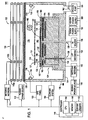
- Figure 1 is a schematic sectional view of one embodiment of an etch reactor suitable for etching a chromium layer
- Figure 2 is a flow diagram of one embodiment of a method for etching a chromium layer
- Figures 3A-I are one embodiment of quartz photomask fabricated utilizing one embodiment of the chromium layer etch method of the present invention
- Figures 4A-G are one embodiment of quartz phase shift mask fabricated utilizing one embodiment of the chromium layer etch method of the present invention.
- Figures 5A-F are one embodiment of quartz phase shift mask fabricated utilizing one embodiment of the chromium layer etch method of the present invention.
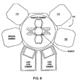
- Figure 6 is a schematic diagram of one embodiment of a processing system, e.g., a cluster tool, including the reactor of Figure 1 .
- FIG 1 depicts a schematic diagram of one embodiment of an etch processing chamber 100 in which a method of quartz etching of the present invention may be practiced.
- Suitable reactors that may be adapted for use with the teachings disclosed herein include, for example, the Decoupled Plasma Source (DPS ® ) II reactor, or the Tetra I and Tetra II Photomask etch systems, all of which are available from Applied Materials, Inc. of Santa Clara, California.
- the etch processing chamber 100 may also be used as a processing module of a processing system 170 as shown in Figure 6 , such as, for example, a Centura ® integrated semiconductor wafer processing system, also available from Applied Materials, Inc.
- the processing system may also include a first chamber 172 suitable for ashing and a second chamber suitable for polymer deposition 174.
- suitable ashing and deposition chambers include AXIOM HTTM and Tetra II processing chamber, also available from Applied Materials, Inc.
- the particular embodiment of the processing chamber 100 shown herein is provided for illustrative purposes and should not be used to limit the scope of the invention.
- the processing chamber 100 generally comprises a process chamber body 102 having a substrate pedestal 124, and a controller 146.
- the chamber body 102 has a conductive wall 104 that supports a substantially flat dielectric ceiling 108.
- Other embodiments of the processing chamber 100 may have other types of ceilings, e.g ., a dome-shaped ceiling.
- An antenna 110 is disposed above the ceiling 108.
- the antenna 110 comprises one or more inductive coil elements that may be selectively controlled (two co-axial elements 110a and 110b are shown in Figure 1 ).
- the antenna 110 is coupled through a first matching network 114 to a plasma power source 112.
- the plasma power source 112 is typically capable of producing up to about 3000 Watts (W) at a tunable frequency in a range from about 50 kHz to about 13.56 MHz. In one embodiment, the plasma power source 112 provides about 100 to about 600 W of inductively coupled RF power, and in another embodiment, the plasma power source 112 provides about 250 to about 600 W of inductively coupled RF power.
- the substrate pedestal (cathode) 124 is coupled through a second matching network 142 to a biasing power source 140.
- the biasing source 140 provides between about zero to about 600 W at a tunable pulse frequency in the range of about 1 to about 10 kHz.
- the biasing source 140 is capable of producing a pulsed RF power output.
- the biasing source 140 may produce pulsed DC power output. It is contemplated that the source 140 may also be configured to provide a constant DC and/or RF power output.
- the biasing source 140 is configured to provide pulsed RF power less than about 600 Watts at a frequency between about 1 to about 10 kHz, with a duty cycle between about 10 to about 95 percent. In another embodiment, the biasing source 140 is configured to provide pulsed RF power between about 10 to about 150 W, at a frequency between about 2 to about 5 kHz, with a duty cycle between about 80 to about 95 percent. In yet another embodiment, the biasing source provides a pulsed RF power of about 10 W.
- the substrate support pedestal 124 includes an electrostatic chuck 160.
- the electrostatic chuck 160 comprises at least one clamping electrode 132 and is controlled by a chuck power supply 166.
- the substrate pedestal 124 may comprise substrate retention mechanisms such as a susceptor clamp ring, a mechanical chuck, and the like.
- a gas panel 120 is coupled to the processing chamber 100 to provide process and/or other gases to the interior of the process chamber 102.
- the gas panel 120 is coupled to one or more inlets 116 formed in a channel 118 in the sidewall 104 of the chamber 102. It is contemplated that the one or more inlets 116 may be provided in other locations, for example, in the ceiling 108 of the processing chamber 100.
- the gas panel 120 is adapted to provide fluorinated process gas through the inlets 116 and into the interior of the chamber body 102.
- a plasma is formed from the process gas and maintained through inductive coupling of power from the plasma power source 112.
- the plasma may alternatively be formed remotely or ignited by other methods.
- the process gas provided from the gas panel 120 includes at least a fluorinated gas and a carbon containing gas. Examples of fluorinated and carbon containing gases include CHF 3 and CF 4 . Other fluorinated gases may include one or more of C 2 F, C 4 F 6 , C 3 F 8 and C 5 F 8 .
- the pressure in the processing chamber 100 is controlled using a throttle valve 162 and a vacuum pump 164.
- the vacuum pump 164 and throttle valve 162 are capable of maintaining chamber pressures in the range of about 1 to about 20 mTorr.
- the temperature of the wall 104 may be controlled using liquid-containing conduits (not shown) that run through the wall 104. Wall temperature is generally maintained at about 65 degrees Celsius.
- the chamber wall 104 is formed from a metal (e.g ., aluminum, stainless steel, and the like) and is coupled to an electrical ground 106.
- the processing chamber 100 also comprises conventional systems for process control, internal diagnostic, end point detection, and the like. Such systems are collectively shown as support systems 154.
- a reticle adapter 182 is used to secure a substrate (such as a reticle or other workpiece) 122 onto the substrate support pedestal 124.
- the reticle adapter 182 generally includes a lower portion 184 milled to cover an upper surface of the pedestal 124 (for example, the electrostatic chuck 160) and a top portion 186 having an opening 188 that is sized and shaped to hold the substrate 122.
- the opening 188 is generally substantially centered with respect to the pedestal 124.
- the adapter 182 is generally formed from a single piece of etch resistant, high temperature resistant material such as polyimide ceramic or quartz.
- a suitable reticle adapter is disclosed in United States Patent No. 6,251,217, issued on June 26, 2001 .
- An edge ring 126 may cover and/or secure the adapter 182 to the pedestal 124.
- a lift mechanism 138 is used to lower or raise the adapter 182, and hence, the substrate 122, onto or off of the substrate support pedestal 124.
- the lift mechanism 138 comprises a plurality of lift pins (one lift pin 130 is shown) that travel through respective guide holes 136.
- the temperature of the substrate 122 is controlled by stabilizing the temperature of the substrate pedestal 124.
- the substrate support pedestal 124 comprises a heater 144 and an optional heat sink 128.
- the heater 144 may be one or more fluid conduits configured to flow a heat transfer fluid therethrough.
- the heater 144 may include at least one heating element 134 that is regulated by a heater power supply 168.
- a backside gas e.g., helium (He)
- He helium
- the backside gas is used to facilitate heat transfer between the pedestal 124 and the substrate 122.
- the pedestal 124 may be heated by the embedded heater 144 to a steady-state temperature, which in combination with the helium backside gas, facilitates uniform heating of the substrate 122.
- An ion-radical shield 127 is disposed in the chamber body 102 above the pedestal 124.
- the ion-radical shield 127 is electrically isolated from the chamber walls 104 and the pedestal 124 and generally comprises a substantially flat plate 131 having a plurality of apertures 129.
- the shield 127 is supported in the chamber 102 above the pedestal by a plurality of legs 125.
- the apertures 129 define a desired open area in the surface of the shield 127 that controls the quantity of ions that pass from a plasma formed in an upper process volume 178 of the process chamber 102 to a lower process volume 180 located between the ion-radical shield 127 and the substrate 122.
- the shield 127 is an ion filter.
- One example of a suitable shield that may be adapted to benefit from the invention is described in United States Patent Application US 2006/0000802 A1, filed June 30, 2004 by Kumar et al. , entitled “METHOD AND APPARATUS FOR PHOTOMASK PLASMA ETCHING" .
- the controller 146 comprises a central processing unit (CPU) 150, a memory 148, and support circuits 152 for the CPU 150 and facilitates control of the components of the processing chamber 100 and, as such, of the etch process, as discussed below in further detail.
- the controller 146 may be one of any form of general-purpose computer processor that can be used in an industrial setting for controlling various chambers and sub-processors.
- the memory 148 of the CPU 150 may be one or more of readily available memory such as random access memory (RAM), read only memory (ROM), floppy disk, hard disk, or any other form of digital storage, local or remote.
- the support circuits 152 are coupled to the CPU 150 for supporting the processor in a conventional manner.
- circuits include cache, power supplies, clock circuits, input/output circuitry and subsystems, and the like.
- the inventive method is generally stored in the memory 148 or other computer-readable medium accessible to the CPU 150 as a software routine.
- software routine may also be stored and/or executed by a second CPU (not shown) that is remotely located from the hardware being controlled by the CPU 150.
- Figure 2 is a flow diagram of one embodiment of a method 200 for etching chromium. Although the method 200 is described below with reference to a substrate utilized to fabricate a photomask, the method 200 may also be used to advantage in other chromium etching applications.
- the method 200 begins at step 202 when the substrate 122 is placed on a support pedestal 124.
- the substrate 122 rests in the opening 188 of the adapter 182.
- the substrate 122 depicted in Figure 1 includes an optically transparent silicon based material, such as quartz (i.e., silicon dioxide (SiO 2 )) layer 192, having an opaque light-shielding chromium layer 190, known as a photomask material, forming a patterned mask on the surface of the quartz layer 192.
- the chromium layer 190 may be chromium and/or chromium oxynitride.
- the substrate 122 may also include an attenuating layer (not shown), such as silicon nitride (SiN) doped with molybdenum (Mo) or molybdenum silicon (MoSi), interposed between the quartz layer 192 and chromium layer 190.
- an attenuating layer such as silicon nitride (SiN) doped with molybdenum (Mo) or molybdenum silicon (MoSi), interposed between the quartz layer 192 and chromium layer 190.
- a resist layer is patterned over the chromium layer.
- the resist layer may be patterned by any suitable method.
- a conformal protective layer is deposited over the patterned resist layer.
- the protective layer may be a polymer, such as carbon polymer with hydrogen.
- the protective layer may be deposited to a thickness of between about 100 to about 500 Angstroms, and in another embodiment, is between about 150 to about 200 Angstroms.
- the protective layer is deposited by using a plasma formed from one or more fluorocarbon processing gases, for example, CHF 3 and/or C 4 F 8 , among others.
- the plasma may include Ar, which improves deposition uniformity.
- the protective layer may be deposited using a plasma power of between about 200 and about 500 W, a bias power between about 0 to about 20 W. In another embodiment, the bias power is less than about 10 W.
- One exemplary process gas utilized to form the protective layer in a plasma process uses about 100 sccm CHF 3 and about 100 sccm Ar, and is maintained at a chamber pressure of about 3 to about 20 milliTorr to form the protective layer up to about 500 Angstroms thick.
- the chromium layer is etched using the patterned resist (and protective layer, when present) as an etch mask.
- the chromium etching step 208 may include first removing the horizontal portions of the protective layer disposed in the openings of the patterned resist to exposed portions of the chromium layer. As the vertical portions of the protective layer disposed on the sidewalls of the patterned resist are removed very slowly as compared to the horizontal portions of the protective layer, chromium layer is etch while the protective layer disposed on the sidewalls of the patterned resist substantially retains its critical dimension (CD) of the opening, thereby allowing accurate transfer of the mask CD to the opening formed in the chromium layer during the etch step 208.
- CD critical dimension
- the etch step 208 forming a plasma from one or more halogen containing process gases are introduced into the process chamber 102 through the gas inlet 116.
- exemplary process gases may include one or more of a fluorocarbon gas, Cl 2 , HBr, HCl, CF 4 and CHF 3 , among others.
- the processing gas may also include O 2 .
- the processing gas may further include an inert gas, such as He, Ar, Xe, Ne, and Kr.
- the substrate 122 comprising chromium is etched using the Tetra I, Tetra II, or DPS ® II etch module by providing CF 4 at a rate of 2 to 50 standard cubic centimeters per minute (sccm) and CFH 3 at a rate of 10 to 50 sccm.
- One specific process recipe provides CF 4 at a rate of 9 sccm, CHF 3 at a rate of 26 sccm.
- the pressure in the process chamber is controlled to less than about 40 mTorr, and in one embodiment, between about 1.5 and about 15 mTorr.
- a pulsed bias power of less than about 600 W is applied to the support pedestal 124 to bias the substrate 122.
- the substrate 112 is biased with a pulsed RF power of less than about 150 W, and in a second example, the substrate 112 is biased with a pulsed RF of about 10 W.
- the bias power may be pulsed with a frequency and duty cycle as described above, for example, with a frequency in the range of about 1 to about 10 kHz, and with a duty cycle between about 10 to about 95 percent.
- the pulsed bias power may be DC and/or RF.
- the biasing source 140 provides pulsed RF power between about 10 to about 150 W, at a frequency between about 2 to about 5 kHz, with a duty cycle between about 80 to about 95 percent. In yet another embodiment, the biasing source provides a pulsed RF power of about 10 W.
- plasma formed from the process gases, is maintained by applying RF power of between about 250 to about 600 W from the plasma power source 112 to the antenna 110. It is contemplated that the plasma may be ignited by any number of methods.
- the chromium layer 190 exposed on the substrate 122 is etched until an endpoint is reached.
- the endpoint may be determined by time, optical interferometry, chamber gas emission spectrography or by other suitable methods.
- the etching step may be performed in-situ the processing system 170 or processing chamber 100 in which the deposition step 206 was performed.
- the chromium layer 190 disposed on the substrate 122 is predominantly etched by the radicals formed by the plasma while the quantity of ions striking the substrate 122 is controlled.
- the reduction in ion impingement on the substrate 122 reduces the etch bias as the resist mask is not attached as aggressively compared to conventional etch processes, resulting in improved accuracy of critical dimensions transfer from the mask to the etched layer.
- the ion-radical shield allows use of other chromium etch processes, for example, the etch process is described in United States Patent Application US 2003/04994, filed September 4, 2002 . It is contemplated that other suitable metal etch processes may be utilized.
- the resist and protective layer remaining after the etch step 208 is removed.
- the remaining resist and protective layer is removed by ashing. Removal step 210 may be performed in-situ the processing system 170 or processing chamber 100 in which the etching step 208 was performed.
- Advantages of the chromium etch method 200 over conventional etch methods includes reduced etch bias; thus making the method 200 highly desirable in etch applications producing small critical dimensions. Moreover, as the chromium etch method 200 allows more accurately transfers critical dimensions from the resist to openings formed in the chromium layer, layers subsequently etched using the patterned chromium layer exhibit good transfer of critical dimensions, thereby making the method 200 highly desirable for fabrication of masks having small line width, such as 45nm node applications.
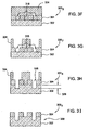
- Figures 3A-G depict one embodiment of a film stack 300 fabricated into a quartz photomask 340 utilizing the method 200 described above.
- the subscript "i" is an integer representing different fabrication stages the film stack shown in Figures 3A-G .
- the film stack 300 1 depicted in Figure 3A includes a quartz layer 302 having a chromium layer 304 disposed thereon.
- the chromium layer 304 is typically chromium and/or chromium oxide such as those described above.
- An optional antireflection layer 306 (shown in phantom) may be formed on the chromium layer 304.
- the antireflection layer 306 may be a thin layer chromium oxide or other suitable material.
- a first resist layer 308 is disposed on the chromium layer 304 or antireflection layer 306, when present.
- the first resist layer 308 is patterned and utilized as a etch mask to etch the chromium layer 304 to form features 320 exposing the underlying quartz layer 302 as depicted in the film stack 300 2 illustrated in Figure 3B .
- a conformal protective layer 310 may be deposited over the resist 308.
- the protective layer 310 covers the sidewalls of the features 320 formed in the resist 308 with a predefined thickness to define a trench 314 having a width 316 as shown in the film stack 300 3 illustrated in Figure 3C .
- the width 316 is selected to have a predefined critical dimension to be transferred to the chromium layer 304.
- the chromium layer 304 is etched using the method 200.
- the chromium layer 304 is etched using a plasma formed from chlorine-containing gas (such as Cl 2 ) or fluorine-containing gases (such as SF 6 or CF 4 ).
- the etch process is substantially anisotropic, thereby breaking through the protective layer (when present) at the bottom of the trench 314 to expose and subsequently etch the chromium layer without significantly changing the width 316.
- the critical dimension, now embodied by width 316 is transferred to an opening 318 formed in the chromium layer 304 as shown in the film stack 300 4 illustrated in Figure 3D .
- the remaining first resist layer 308 is removed, for example, by ashing, to leave the film stack 300 5 as shown in Figure 3E .
- the removal process for the resist layer 308 additionally removes the remaining protective layer 310, leaving a binary photomask 340.
- the film stack 300 5 may be further processed to form a phase shift mask as shown in Figures 3F-I .
- a second resist layer 324 is first disposed on the film stack 300 5 , filling the openings 318 as shown in the film stack 300 6 illustrated in Figure 3F .
- the second resist layer 324 is then patterned.
- the patterned second resist layer 324 exposes the quartz layer 302 at the bottom of alternating openings 318, as shown in the film stack 300 7 illustrated in Figure 3G .
- the quartz layer 302 exposed through the patterned second resist layer 312 is etched using a plasma formed from one or more fluorinated process gases.
- exemplary process gases may include CF 4 and CHF 3 , among others.
- the processing gas may further include an inert gas, such as He, Ar, Xe, Ne, and Kr.
- the bias power applied to the substrate support may be pulsed as described above.
- the endpoint of the quartz etch is selected such that a depth 328 of an etched quartz trench 326 shown in the film stack 300 8 illustrated in Figure 3H is about equal to the length of 180 degrees phase shift through the quartz layer 302 for a predefined wavelength of light intended for use with the quartz phase shift mask. Typical wavelengths are 193 and 248 nm. Thus, the depth 328 is typically about either 172 or 240 nm, although other depths may be utilized for masks intended for use with different lithographic light wavelengths.
- the remaining second resist layer 324 is removed, for example, by ashing, such that the remaining film stack 300 9 forms a quartz phase shift mask 330 as shown in Figure 3I .
- Figures 4A-G depict one embodiment of a film stack 400 i fabricated into a quartz phase shift mask 418 utilizing the method 200 described above.
- the subscript "i" is an integer representing different fabrication stages the film stack shown in Figures 4A-G .
- the film stack 400 1 depicted in Figure 4A includes a quartz layer 402 having a chromium layer 404 disposed thereon.
- the chromium layer 404 is typically chromium and/or chromium oxide such as those described above.
- An optional antireflection layer 406 (shown in phantom) may be disposed on the chromium layer 404.
- a first resist layer 408 is disposed on the chromium layer 404 or antireflection layer 406, when present.
- the first resist layer 408 is patterned to form openings 430 exposing the chromium layer 404, as shown in the film stack 400 2 illustrated in Figure 3B .
- An optional conformal protective layer 432 may be deposited in the chromium layer 404 and first resist layer 408, covering the sidewalls and bottom of the opening 430 as shown in the film stack 400 3 illustrated in Figure 4C .
- the protective layer 432 may be deposited as described with reference to the protective layer 310 above.
- the thickness of the protective layer 432 is selected such that the feature 434 defined between the vertical portions of the protective layer 432 has a predetermined width 436.
- the protective layer 432 and first resist layer 408 are used as a mask to etch an opening 410 in the chromium layer 404, exposing the underlying quartz layer 402 as depicted in the film stack 400 4 illustrated in Figure 4D .
- the etch process is substantially anisotropic, thereby breaking through the protective layer 432 at the bottom of the feature 434 to expose and subsequently etch the chromium layer 404 without significantly changing the width 436.
- the critical dimension of defined by the feature 410 is transferred to an opening 438 formed in the chromium layer 304.
- the chromium layer 404 may be etched as described above.
- the chromium layer 404 is then utilized as an etch mask for etching the quartz layer 402.
- the quartz layer 402 may be etch as described above to form a trench 440 having a bottom 416.
- the etching of the quartz layer 404 through the openings 438 substantially transferred the width 436 to the trench 440.
- the endpoint of the quartz etch is selected such that a depth 414 of an etched quartz trench 440 shown in the film stack 400 5 illustrated in Figure 4F is about equal to the length of 180 degrees phase shift through the quartz layer 402 for a predefined wavelength of light intended for use with the quartz phase shift mask as described above.
- the remaining chromium layer 404 is removed by a suitable process, for example, by a chromium etch as described above, to leave the film stack 400 6 as a quartz phase shift mask 442, shown in the film stack 400 7 illustrated in Figure 4G .
- Figures 5A-F depict one embodiment of a film stack 500 i fabricated into a chromeless etch lithography mask 540 utilizing the method 200 described above.
- the subscript "i" is an integer representing different fabrication stages the film stack shown in Figures 5A-F .
- the film stack 500 1 depicted in Figure 5A includes a quartz layer 502 having a photomask layer 504 disposed thereon.
- the photomask layer 504 includes a chromium layer 552, for example, chromium and/or chromium oxide as those described above, over an attenuating layer 554.
- the attenuating layer 554 generally has a thickness about equal to the length of 180 degrees phase shift through the quartz layer 502 for a predefined wavelength of light intended for use with the quartz phase shift mask. Typical wavelengths are 193 and 248 nm. Thus, the thickness of the attenuating layer is typically about 50 to about 100 nm thick, although other depths may be utilized for masks intended for use with different lithographic light wavelengths and/or different attenuating materials.
- An optional antireflection layer 506 may be formed on the photomask layer 504.
- a first resist layer 508 is disposed on the photomask layer 504 or antireflection layer 506, when present.
- the first resist layer 508 is patterned and utilized as a etch mask to etch the photomask layer 504 to form features 520 exposing the underlying quartz layer 502 as depicted in the film stack 500 2 illustrated in Figure 5B .
- An optional conformal protective layer 510 may be deposited over the resist 508.
- the protective layer 510 covers the sidewalls of the features 520 formed in the resist 508 with a predefined thickness to define a trench 514 having a width 516 as shown in the film stack 500 3 illustrated in Figure 5C .
- the width 516 is selected to have a predefined critical dimension to be transferred to the photomask layer 504 (e.g., the attenuating layer 554 and the chromium layer 552).
- the photomask layer 504 may be etched in a two step process to first etch the chromium layer 552 followed by an etch of the attenuating layer 554.
- the chromium layer 552 may be etched as described above.
- the etch process is substantially anisotropic, thereby breaking through the portion 512 of the protective layer 510 at the bottom of the trench 514 to expose and subsequently etch the chromium layer without significantly changing the width 516.
- the attenuating layer 554 may be etched using a plasma formed from chlorine-containing gas (such as Cl 2 ) and/or fluorine-containing gases (such as SF 6 or CF 4 ).
- the two step etch process is substantially anisotropic, thereby breaking through the protective layer at the bottom of the trench 514 to expose and subsequently etch the chromium layer without significantly changing the width 516.
- the patterned chromium layer functions as a mask to etch the attenuating layer 554. As such, the critical dimension 516 is transferred to an opening 518 formed in the photomask layer 504 as shown in the film stack 500 4 illustrated in Figure 5D .
- the attenuating layer 554 may be plasma etched by a processing gas including (i) one or more fluorine containing polymerizing materials, (ii) a chlorine containing gas, and optionally, (iii) an inert gas.
- a processing gas including (i) one or more fluorine containing polymerizing materials, (ii) a chlorine containing gas, and optionally, (iii) an inert gas.
- a polymerization limiting or inhibiting gas may also be included in the processing gas.
- the one or more fluorine containing gas may include one or more fluorine containing hydrocarbons, hydrogen free fluorine containing gases, or combinations thereof.
- the one or more fluorine containing hydrocarbons may have the general formula C x H y F z , wherein x is an integer from 1 to 5 of carbon atoms, y is an integer from 1 to 8 of hydrogen atoms, and z is an integer from 1 to 8 of fluorine atoms.
- fluorine containing hydrocarbon gases include CHF 3 , CH 3 F, CH 2 F 2 , C 2 HF 5 , C 2 H 4 F 2 , and combinations thereof.
- Fluorine containing hydrocarbon gases having from 1 to 2 atoms of carbon, from 1 to 4 atoms of hydrogen, and from 1 to 5 atoms of fluorine, such as CHF 3 , may be used when etching the attenuating layer 554.
- the hydrogen free fluorocarbon gases may have from 1 to 5 atoms of carbon and from 4 to 8 atoms of fluorine.
- hydrogen free fluorocarbon gases include CF 4 , C 2 F 6 , C 4 F 6 , C 3 F 8 , C 4 F 8 , C 5 F 8 , and combinations thereof.
- the processing gas may include additional etching gases for example, sulfur fluorides, such as sulfur hexafluoride (SF 6 ).
- Fluorine containing gases may be advantageously used to form passivating polymer deposits on the surfaces, particularly the sidewalls, of openings formed in a patterned resist material and etched optically transparent materials.
- the passivating polymer deposits prevent excessive etching of the feature definitions, improving the transfer of the planned critical dimensions to the attenuating layer 554.
- a plasma formed from one or more fluorine containing hydrocarbon gases produces fluorine-containing species that etch the attenuating layer 554 on the substrate 122 without the presence of an oxidizing gas.
- the chlorine-containing gases are selected from the group of chlorine (Cl 2 ), carbon tetrachloride (CCl 4 ), hydrochloric acid (HCl), and combinations thereof, and are used to supply highly reactive radicals to etch the optically transparent material.
- the chlorine-containing gas provides a source of etching radicals and hydrogen or carbon-containing chlorine-containing gases may provide a source of material for forming passivating polymer deposits, which may improve etch bias.
- the processing gas may also include an inert gas which, when ionized as part of the plasma comprising the processing gas, results in sputtering species to increase the etching rate of the feature definitions.
- the presence of an inert gas as part of the plasma may also enhance dissociation of the processing gas.
- inert gases added to the process gas form ionized sputtering species and may further sputter-off any formed polymer deposits on the sidewalls of the freshly etched feature definitions, thereby reducing any passivating deposits and providing a controllable etch rate. It has been observed that the inclusion of an inert gas into the processing gas provides improved plasma stability and improved etching uniformity.
- inert gases include argon (Ar), helium (He), neon (Ne), xenon (Xe), krypton (Kr), and combinations thereof, of which argon and helium are generally used.
- the processing gas for etching the attenuating layer 554 may include chlorine (Cl 2 ) gas, trifluoromethane (CHF 3 ), and argon as an inert gas.
- the processing gas may include one or more polymerization limiting gases, such as oxygen, ozone, nitrogen, or combinations thereof, may be used to control the etching rates of the processing gas by controlling the formation and removal of passivating polymer deposits on the substrate.
- Oxygen containing gases enhance the formation of free oxygen species that react with other species to reduce the formation of polymers that deposit on the surfaces of the etched feature definitions as passivating deposits.
- oxygen gases react with some of the radicals of the plasma process, such as CF 2 , to form volatile radicals, such as COF 2 , which are exhausted from the processing chamber.
- the total flow rate of the processing gases are introduced at a flow rate of greater than about 15 sccm, such as between about 15 sccm and about 200 sccm for etching a 150 mm by 150 mm square photolithographic reticle substrate in an etch chamber.
- the chlorine-containing gas is introduced into the processing chamber at a flow rate of between about 5 sccm and about 100 sccm for etching a 150 mm by 150 mm square photolithographic reticle substrate.
- a flow rate between about 1 sccm and about 50 sccm is used for etching a 150 mm by 150 mm square photolithographic reticle substrate.
- a flow rate between about 0 sccm and about 100 sccm is used for etching a 150 mm by 150 mm square photolithographic reticle substrate.
- polymerization limiting gases are introduced into the processing chamber, a flow rate between about 1 sccm and about 100 sccm is used for etching a 150 mm by 150 mm square photolithographic reticle substrate.
- the individual and total gas flows of the processing gases may vary based upon a number of processing factors, such as the size of the processing chamber, the size of the substrate being processed, and the specific etching profile desired by the operator.
- the processing chamber pressure is maintained between about 2 milliTorr and about 50 millTorr.
- a chamber pressure between about 3 milliTorr and about 20 milliTorr, for example, 3 milliTorr and 10 milliTorr, may be maintained during the etching process.
- the remaining first resist layer 508 is removed, for example, by ashing, to leave the film stack 500 5 as shown in Figure 5E .
- the removal process for the resist layer 508 additionally removes the remaining protective layer 510.
- the chromium portion of the photomask layer 504 (e.g., the patterned chromium layer 552) is removed by a suitable process, such as a dry etch process as described above.
- a suitable process such as a dry etch process as described above.
- the quartz layer 502 and patterned MoSi layer 554 remaining from the film stack 500 6 forms as a chromeless etch lithography mask 540 shown in Figure 5F .
- a method for etching a chromium layer has been provided that advantageously improves trench attributes over conventional processes. Accordingly, the method of etching a chromium layer described herein advantageously facilitates fabrication of photomasks suitable for patterning features having small critical dimensions.
Description
- Embodiments of the present invention generally relate to a method for plasma etching chromium and, more specifically, to a method for etching a chromium layer during photomask fabrication.
- In the manufacture of integrated circuits (IC), or chips, patterns representing different layers of the chip are created by a chip designer. A series of reusable masks, or photomasks, are created from these patterns in order to transfer the design of each chip layer onto a semiconductor substrate during the manufacturing process. Mask pattern generation systems use precision lasers or electron beams to image the design of each layer of the chip onto a respective mask. The masks are then used much like photographic negatives to transfer the circuit patterns for each layer onto a semiconductor substrate. These layers are built up using a sequence of processes and translate into the tiny transistors and electrical circuits that comprise each completed chip. Thus, any defects in the mask may be transferred to the chip, potentially adversely affecting performance. Defects that are severe enough may render the mask completely useless. Typically, a set of 15 to 30 masks is used to construct a chip and can be used repeatedly.
- A mask is typically a glass or a quartz substrate that has a layer of chromium on one side. The chromium layer is covered with an anti-reflective coating and a photosensitive resist. During a patterning process, the circuit design is written onto the mask by exposing portions of the resist to ultraviolet light, making the exposed portions soluble in a developing solution. The soluble portion of the resist is then removed, allowing the exposed underlying chromium to be etched. The etch process removes the chromium and anti-reflective layers from the mask at locations where the resist was removed, i.e., the exposed chromium is removed.
- Another mask utilized for patterning is known as a quartz phase shift mask. The quartz phase shift mask is similar to the mask described above, except that alternating adjacent areas of quartz regions exposed through the patterned chromium layer are etched to a depth about equal to half the wavelength of light which will be utilized to transfer the circuit patterns to a substrate during fabrication. The chromium layer is removed after quartz etching. Thus, as the light is shown through the quartz phase shift mask to expose resist disposed on the substrate, the light impinging the resist through one opening in the mask is 180 degrees out of phase relative to the light passing through the immediately adjacent opening. Therefore, light that may be scattered at the edges of the mask opening is cancelled out by the 180 degree out of phase light scattering at the edge of the adjacent opening, causing a tighter distribution of light in a predefined region of the resist. The tighter distribution of light facilitates writing of features having smaller critical dimensions. Similarly, masks used for chromeless etch lithography also utilize the phase shift of light passing through quartz portions of two masks to sequentially image the resist, thereby improving the light distribution utilized to develop the resist pattern. The phase shift of light through the mask may also be realized using a patterned layer of silicon nitride (SiN) doped with molybdenum (Mb) that caused the imaging light passing through the patterned portions of mask to be 180 degrees out of phase to the light passing through the quartz substrate exposed through openings in the patterned layer.
- In one etch process, known as dry etching, reactive ion etching, or plasma etching, a plasma is used to enhance a chemical reaction and etch the patterned chromium area of the mask.
- Document
EP 1679741 A1 (publication date 12 July 2006) discloses a method of etching quartz. The method includes providing a filmstack in an etching chamber, the filmstack having a quartz layer partially exposed through a patterned layer, providing at least one fluorocarbon process gas to the processing chamber, biasing a quartz layer disposed on a substrate support in the processing chamber with a plurality of power pulses less than 600 Watts and etching the quartz layer through the patterned mask. - Moreover, document
EP 1612840 A1 (publication date 4 January 2006) discloses a method of etching a photomask. The method includes providing a process chamber having a substrate support pedestal adapted to receive a photomask substrate thereon. An ion-radical shield is disposed above the pedestal. A substrate is placed upon the pedestal beneath the ion-radical shield. A process gas is introduced into the process chamber and a plasma is formed from the process gas. The substrate is etched predominantly with radicals that pass through the shield. - Furthermore, from document
US 2003/089680 A1 an apparatus and method for etching a photomask using an inductively coupled pulsed plasma is known. - Undesirably, conventional chromium etch processes often exhibit etch bias due to attack on the photoresist material utilized to pattern the chromium layer. As the resist is attacked during the chromium etch, the critical dimension of patterned resist is not accurately transferred to the chromium layer. Thus, conventional chromium etch processes may not produce acceptable results for masks having critical dimensions less than about 5 µm. This results in non-uniformity of the etched features of the mask and correspondingly diminishes the ability to produce features for devices having small critical dimensions using the mask.
- As the critical dimensions of mask continue to shrink, the importance of etch uniformity increases. Thus, a chromium etch process having high etch uniformity is highly desirable.
- Thus, there is a need for an improved chromium etch process.
- The present invention generally provides a method for etching a chromium layer. The object of the invention is achieved by the measures of appended
claims 1 to 16. - So that the manner in which the features of the present invention can be understood in detail, a more particular description of the invention, is given by reference to embodiments, some of which are illustrated in the appended drawings. It is to be noted, however, that the appended drawings illustrate only typical embodiments of this invention and are therefore not to be considered limiting of its scope, for the invention may admit to other equally effective embodiments.
-
Figure 1 is a schematic sectional view of one embodiment of an etch reactor suitable for etching a chromium layer; -
Figure 2 is a flow diagram of one embodiment of a method for etching a chromium layer; -
Figures 3A-I are one embodiment of quartz photomask fabricated utilizing one embodiment of the chromium layer etch method of the present invention; -
Figures 4A-G are one embodiment of quartz phase shift mask fabricated utilizing one embodiment of the chromium layer etch method of the present invention; -
Figures 5A-F are one embodiment of quartz phase shift mask fabricated utilizing one embodiment of the chromium layer etch method of the present invention; and -
Figure 6 is a schematic diagram of one embodiment of a processing system, e.g., a cluster tool, including the reactor ofFigure 1 . - To facilitate understanding, identical reference numerals have been used, where possible, to designate identical elements that are common to the figures. It is also contemplated that features of one embodiment may be beneficially incorporated in other embodiments, including those not explicitly described, without a specific description of the combined embodiment.
-
Figure 1 depicts a schematic diagram of one embodiment of anetch processing chamber 100 in which a method of quartz etching of the present invention may be practiced. Suitable reactors that may be adapted for use with the teachings disclosed herein include, for example, the Decoupled Plasma Source (DPS®) II reactor, or the Tetra I and Tetra II Photomask etch systems, all of which are available from Applied Materials, Inc. of Santa Clara, California. Theetch processing chamber 100 may also be used as a processing module of aprocessing system 170 as shown inFigure 6 , such as, for example, a Centura® integrated semiconductor wafer processing system, also available from Applied Materials, Inc. The processing system may also include afirst chamber 172 suitable for ashing and a second chamber suitable forpolymer deposition 174. Examples of suitable ashing and deposition chambers include AXIOM HT™ and Tetra II processing chamber, also available from Applied Materials, Inc. The particular embodiment of theprocessing chamber 100 shown herein is provided for illustrative purposes and should not be used to limit the scope of the invention. - Returning to
Figure 1 , theprocessing chamber 100 generally comprises aprocess chamber body 102 having asubstrate pedestal 124, and acontroller 146. Thechamber body 102 has aconductive wall 104 that supports a substantially flatdielectric ceiling 108. Other embodiments of theprocessing chamber 100 may have other types of ceilings, e.g., a dome-shaped ceiling. Anantenna 110 is disposed above theceiling 108. Theantenna 110 comprises one or more inductive coil elements that may be selectively controlled (twoco-axial elements Figure 1 ). Theantenna 110 is coupled through a first matchingnetwork 114 to aplasma power source 112. Theplasma power source 112 is typically capable of producing up to about 3000 Watts (W) at a tunable frequency in a range from about 50 kHz to about 13.56 MHz. In one embodiment, theplasma power source 112 provides about 100 to about 600 W of inductively coupled RF power, and in another embodiment, theplasma power source 112 provides about 250 to about 600 W of inductively coupled RF power. - The substrate pedestal (cathode) 124 is coupled through a
second matching network 142 to a biasingpower source 140. The biasingsource 140 provides between about zero to about 600 W at a tunable pulse frequency in the range of about 1 to about 10 kHz. The biasingsource 140 is capable of producing a pulsed RF power output. Alternatively, the biasingsource 140 may produce pulsed DC power output. It is contemplated that thesource 140 may also be configured to provide a constant DC and/or RF power output. - In one embodiment, the biasing
source 140 is configured to provide pulsed RF power less than about 600 Watts at a frequency between about 1 to about 10 kHz, with a duty cycle between about 10 to about 95 percent. In another embodiment, the biasingsource 140 is configured to provide pulsed RF power between about 10 to about 150 W, at a frequency between about 2 to about 5 kHz, with a duty cycle between about 80 to about 95 percent. In yet another embodiment, the biasing source provides a pulsed RF power of about 10 W. - In one embodiment configured as a DPS® reactor, the
substrate support pedestal 124 includes anelectrostatic chuck 160. Theelectrostatic chuck 160 comprises at least oneclamping electrode 132 and is controlled by achuck power supply 166. In alternative embodiments, thesubstrate pedestal 124 may comprise substrate retention mechanisms such as a susceptor clamp ring, a mechanical chuck, and the like. - A
gas panel 120 is coupled to theprocessing chamber 100 to provide process and/or other gases to the interior of theprocess chamber 102. In the embodiment depicted inFigure 1 , thegas panel 120 is coupled to one ormore inlets 116 formed in achannel 118 in thesidewall 104 of thechamber 102. It is contemplated that the one ormore inlets 116 may be provided in other locations, for example, in theceiling 108 of theprocessing chamber 100. - In one embodiment, the
gas panel 120 is adapted to provide fluorinated process gas through theinlets 116 and into the interior of thechamber body 102. During processing, a plasma is formed from the process gas and maintained through inductive coupling of power from theplasma power source 112. The plasma may alternatively be formed remotely or ignited by other methods. In one embodiment, the process gas provided from thegas panel 120 includes at least a fluorinated gas and a carbon containing gas. Examples of fluorinated and carbon containing gases include CHF3 and CF4. Other fluorinated gases may include one or more of C2F, C4F6, C3F8 and C5F8. - The pressure in the
processing chamber 100 is controlled using athrottle valve 162 and avacuum pump 164. Thevacuum pump 164 andthrottle valve 162 are capable of maintaining chamber pressures in the range of about 1 to about 20 mTorr. - The temperature of the
wall 104 may be controlled using liquid-containing conduits (not shown) that run through thewall 104. Wall temperature is generally maintained at about 65 degrees Celsius. Typically, thechamber wall 104 is formed from a metal (e.g., aluminum, stainless steel, and the like) and is coupled to anelectrical ground 106. Theprocessing chamber 100 also comprises conventional systems for process control, internal diagnostic, end point detection, and the like. Such systems are collectively shown assupport systems 154. - A
reticle adapter 182 is used to secure a substrate (such as a reticle or other workpiece) 122 onto thesubstrate support pedestal 124. Thereticle adapter 182 generally includes alower portion 184 milled to cover an upper surface of the pedestal 124 (for example, the electrostatic chuck 160) and atop portion 186 having anopening 188 that is sized and shaped to hold thesubstrate 122. Theopening 188 is generally substantially centered with respect to thepedestal 124. Theadapter 182 is generally formed from a single piece of etch resistant, high temperature resistant material such as polyimide ceramic or quartz. A suitable reticle adapter is disclosed in United States Patent No.6,251,217, issued on June 26, 2001 . Anedge ring 126 may cover and/or secure theadapter 182 to thepedestal 124. - A
lift mechanism 138 is used to lower or raise theadapter 182, and hence, thesubstrate 122, onto or off of thesubstrate support pedestal 124. Generally, thelift mechanism 138 comprises a plurality of lift pins (onelift pin 130 is shown) that travel through respective guide holes 136. - In operation, the temperature of the
substrate 122 is controlled by stabilizing the temperature of thesubstrate pedestal 124. In one embodiment, thesubstrate support pedestal 124 comprises aheater 144 and anoptional heat sink 128. Theheater 144 may be one or more fluid conduits configured to flow a heat transfer fluid therethrough. In another embodiment, theheater 144 may include at least oneheating element 134 that is regulated by aheater power supply 168. Optionally, a backside gas (e.g., helium (He)) from agas source 156 is provided via agas conduit 158 to channels that are formed in the pedestal surface under thesubstrate 122. The backside gas is used to facilitate heat transfer between thepedestal 124 and thesubstrate 122. During processing, thepedestal 124 may be heated by the embeddedheater 144 to a steady-state temperature, which in combination with the helium backside gas, facilitates uniform heating of thesubstrate 122. - An ion-
radical shield 127 is disposed in thechamber body 102 above thepedestal 124. The ion-radical shield 127 is electrically isolated from thechamber walls 104 and thepedestal 124 and generally comprises a substantiallyflat plate 131 having a plurality ofapertures 129. In the embodiment depicted inFigure 1 , theshield 127 is supported in thechamber 102 above the pedestal by a plurality oflegs 125. Theapertures 129 define a desired open area in the surface of theshield 127 that controls the quantity of ions that pass from a plasma formed in anupper process volume 178 of theprocess chamber 102 to alower process volume 180 located between the ion-radical shield 127 and thesubstrate 122. The greater the open area, the more ions can pass through the ion-radical shield 127. As such, the size and distribution of theapertures 129, along with the thickness of theplate 131 controls the ion density involume 180. Consequently, theshield 127 is an ion filter. One example of a suitable shield that may be adapted to benefit from the invention is described in United States Patent ApplicationUS 2006/0000802 A1, filed June 30, 2004 by Kumar et al. , entitled "METHOD AND APPARATUS FOR PHOTOMASK PLASMA ETCHING". - The
controller 146 comprises a central processing unit (CPU) 150, amemory 148, and supportcircuits 152 for theCPU 150 and facilitates control of the components of theprocessing chamber 100 and, as such, of the etch process, as discussed below in further detail. Thecontroller 146 may be one of any form of general-purpose computer processor that can be used in an industrial setting for controlling various chambers and sub-processors. Thememory 148 of theCPU 150 may be one or more of readily available memory such as random access memory (RAM), read only memory (ROM), floppy disk, hard disk, or any other form of digital storage, local or remote. Thesupport circuits 152 are coupled to theCPU 150 for supporting the processor in a conventional manner. These circuits include cache, power supplies, clock circuits, input/output circuitry and subsystems, and the like. The inventive method is generally stored in thememory 148 or other computer-readable medium accessible to theCPU 150 as a software routine. Alternatively, such software routine may also be stored and/or executed by a second CPU (not shown) that is remotely located from the hardware being controlled by theCPU 150. -
Figure 2 is a flow diagram of one embodiment of amethod 200 for etching chromium. Although themethod 200 is described below with reference to a substrate utilized to fabricate a photomask, themethod 200 may also be used to advantage in other chromium etching applications. - The
method 200, which may be stored in computer readable form in thememory 148 of thecontroller 146 or other storage medium, begins atstep 202 when thesubstrate 122 is placed on asupport pedestal 124. In one embodiment, thesubstrate 122 rests in theopening 188 of theadapter 182. Thesubstrate 122 depicted inFigure 1 includes an optically transparent silicon based material, such as quartz (i.e., silicon dioxide (SiO2))layer 192, having an opaque light-shieldingchromium layer 190, known as a photomask material, forming a patterned mask on the surface of thequartz layer 192. Thechromium layer 190 may be chromium and/or chromium oxynitride. Thesubstrate 122 may also include an attenuating layer (not shown), such as silicon nitride (SiN) doped with molybdenum (Mo) or molybdenum silicon (MoSi), interposed between thequartz layer 192 andchromium layer 190. - At
step 204, a resist layer is patterned over the chromium layer. The resist layer may be patterned by any suitable method. - At an
optional step 206, a conformal protective layer is deposited over the patterned resist layer. The protective layer may be a polymer, such as carbon polymer with hydrogen. The protective layer may be deposited to a thickness of between about 100 to about 500 Angstroms, and in another embodiment, is between about 150 to about 200 Angstroms. - In one embodiment, the protective layer is deposited by using a plasma formed from one or more fluorocarbon processing gases, for example, CHF3 and/or C4F8, among others. Optionally, the plasma may include Ar, which improves deposition uniformity. In one embodiment, the protective layer may be deposited using a plasma power of between about 200 and about 500 W, a bias power between about 0 to about 20 W. In another embodiment, the bias power is less than about 10 W. One exemplary process gas utilized to form the protective layer in a plasma process uses about 100 sccm CHF3 and about 100 sccm Ar, and is maintained at a chamber pressure of about 3 to about 20 milliTorr to form the protective layer up to about 500 Angstroms thick.
- At
step 208, the chromium layer is etched using the patterned resist (and protective layer, when present) as an etch mask. Thechromium etching step 208 may include first removing the horizontal portions of the protective layer disposed in the openings of the patterned resist to exposed portions of the chromium layer. As the vertical portions of the protective layer disposed on the sidewalls of the patterned resist are removed very slowly as compared to the horizontal portions of the protective layer, chromium layer is etch while the protective layer disposed on the sidewalls of the patterned resist substantially retains its critical dimension (CD) of the opening, thereby allowing accurate transfer of the mask CD to the opening formed in the chromium layer during theetch step 208. - In one embodiment, the
etch step 208 forming a plasma from one or more halogen containing process gases are introduced into theprocess chamber 102 through thegas inlet 116. Exemplary process gases may include one or more of a fluorocarbon gas, Cl2, HBr, HCl, CF4 and CHF3, among others. The processing gas may also include O2. The processing gas may further include an inert gas, such as He, Ar, Xe, Ne, and Kr. - In another embodiment, the
substrate 122 comprising chromium is etched using the Tetra I, Tetra II, or DPS® II etch module by providing CF4 at a rate of 2 to 50 standard cubic centimeters per minute (sccm) and CFH3 at a rate of 10 to 50 sccm. One specific process recipe provides CF4 at a rate of 9 sccm, CHF3 at a rate of 26 sccm. The pressure in the process chamber is controlled to less than about 40 mTorr, and in one embodiment, between about 1.5 and about 15 mTorr. - During the
chromium etch step 208, a pulsed bias power of less than about 600 W is applied to thesupport pedestal 124 to bias thesubstrate 122. In a first example, thesubstrate 112 is biased with a pulsed RF power of less than about 150 W, and in a second example, thesubstrate 112 is biased with a pulsed RF of about 10 W. The bias power may be pulsed with a frequency and duty cycle as described above, for example, with a frequency in the range of about 1 to about 10 kHz, and with a duty cycle between about 10 to about 95 percent. The pulsed bias power may be DC and/or RF. In another embodiment, the biasingsource 140 provides pulsed RF power between about 10 to about 150 W, at a frequency between about 2 to about 5 kHz, with a duty cycle between about 80 to about 95 percent. In yet another embodiment, the biasing source provides a pulsed RF power of about 10 W. - During
step 208, plasma, formed from the process gases, is maintained by applying RF power of between about 250 to about 600 W from theplasma power source 112 to theantenna 110. It is contemplated that the plasma may be ignited by any number of methods. - The
chromium layer 190 exposed on thesubstrate 122 is etched until an endpoint is reached. The endpoint may be determined by time, optical interferometry, chamber gas emission spectrography or by other suitable methods. The etching step may be performed in-situ theprocessing system 170 orprocessing chamber 100 in which thedeposition step 206 was performed. - With an ion-
radical shield 127 being present, electrons from the plasma bombard theplate 131 to form a potential on the surface of the ion-radical shield 127. This potential attracts the ions present in the plasma and limits the number of ions that pass through theapertures 129 into thelower process volume 180. The neutral radicals in the plasma pass through theapertures 129 in the ion-radical shield 127 into thelower process volume 180. Thus, thechromium layer 190 disposed on thesubstrate 122 is predominantly etched by the radicals formed by the plasma while the quantity of ions striking thesubstrate 122 is controlled. The reduction in ion impingement on thesubstrate 122 reduces the etch bias as the resist mask is not attached as aggressively compared to conventional etch processes, resulting in improved accuracy of critical dimensions transfer from the mask to the etched layer. - The ion-radical shield allows use of other chromium etch processes, for example, the etch process is described in United States Patent Application
US 2003/04994, filed September 4, 2002 .
It is contemplated that other suitable metal etch processes may be utilized. - At
step 210, the resist and protective layer remaining after theetch step 208 is removed. In one embodiment, the remaining resist and protective layer is removed by ashing.Removal step 210 may be performed in-situ theprocessing system 170 orprocessing chamber 100 in which theetching step 208 was performed. - Advantages of the
chromium etch method 200 over conventional etch methods includes reduced etch bias; thus making themethod 200 highly desirable in etch applications producing small critical dimensions. Moreover, as thechromium etch method 200 allows more accurately transfers critical dimensions from the resist to openings formed in the chromium layer, layers subsequently etched using the patterned chromium layer exhibit good transfer of critical dimensions, thereby making themethod 200 highly desirable for fabrication of masks having small line width, such as 45nm node applications. -
Figures 3A-G depict one embodiment of afilm stack 300 fabricated into aquartz photomask 340 utilizing themethod 200 described above. The subscript "i" is an integer representing different fabrication stages the film stack shown inFigures 3A-G . - The
film stack 3001 depicted inFigure 3A includes aquartz layer 302 having achromium layer 304 disposed thereon. Thechromium layer 304 is typically chromium and/or chromium oxide such as those described above. An optional antireflection layer 306 (shown in phantom) may be formed on thechromium layer 304. Theantireflection layer 306 may be a thin layer chromium oxide or other suitable material. A first resistlayer 308 is disposed on thechromium layer 304 orantireflection layer 306, when present. - The first resist
layer 308 is patterned and utilized as a etch mask to etch thechromium layer 304 to formfeatures 320 exposing theunderlying quartz layer 302 as depicted in thefilm stack 3002 illustrated inFigure 3B . - Optionally, a conformal
protective layer 310 may be deposited over the resist 308. Theprotective layer 310 covers the sidewalls of thefeatures 320 formed in the resist 308 with a predefined thickness to define atrench 314 having awidth 316 as shown in thefilm stack 3003 illustrated inFigure 3C . Thewidth 316 is selected to have a predefined critical dimension to be transferred to thechromium layer 304. - The
chromium layer 304 is etched using themethod 200. In one embodiment, thechromium layer 304 is etched using a plasma formed from chlorine-containing gas (such as Cl2) or fluorine-containing gases (such as SF6 or CF4). The etch process is substantially anisotropic, thereby breaking through the protective layer (when present) at the bottom of thetrench 314 to expose and subsequently etch the chromium layer without significantly changing thewidth 316. As such, the critical dimension, now embodied bywidth 316, is transferred to anopening 318 formed in thechromium layer 304 as shown in thefilm stack 3004 illustrated inFigure 3D . - After the
openings 318 are formed in thechromium layer 304, the remaining first resistlayer 308 is removed, for example, by ashing, to leave thefilm stack 3005 as shown inFigure 3E . The removal process for the resistlayer 308 additionally removes the remainingprotective layer 310, leaving abinary photomask 340. - Optionally, the
film stack 3005 may be further processed to form a phase shift mask as shown inFigures 3F-I . To form the phase shift mask, a second resistlayer 324 is first disposed on thefilm stack 3005, filling theopenings 318 as shown in thefilm stack 3006 illustrated inFigure 3F . The second resistlayer 324 is then patterned. Typically when forming a quartz phase shift mask, the patterned second resistlayer 324 exposes thequartz layer 302 at the bottom of alternatingopenings 318, as shown in thefilm stack 3007 illustrated inFigure 3G . - The
quartz layer 302 exposed through the patterned second resistlayer 312 is etched using a plasma formed from one or more fluorinated process gases. Exemplary process gases may include CF4 and CHF3, among others. The processing gas may further include an inert gas, such as He, Ar, Xe, Ne, and Kr. During etching of thequartz layer 302, the bias power applied to the substrate support may be pulsed as described above. - The endpoint of the quartz etch is selected such that a
depth 328 of an etchedquartz trench 326 shown in thefilm stack 3008 illustrated inFigure 3H is about equal to the length of 180 degrees phase shift through thequartz layer 302 for a predefined wavelength of light intended for use with the quartz phase shift mask. Typical wavelengths are 193 and 248 nm. Thus, thedepth 328 is typically about either 172 or 240 nm, although other depths may be utilized for masks intended for use with different lithographic light wavelengths. After thequartz trench 326 is etched, the remaining second resistlayer 324 is removed, for example, by ashing, such that the remainingfilm stack 3009 forms a quartzphase shift mask 330 as shown inFigure 3I . -
Figures 4A-G depict one embodiment of afilm stack 400i fabricated into a quartzphase shift mask 418 utilizing themethod 200 described above. The subscript "i" is an integer representing different fabrication stages the film stack shown inFigures 4A-G . - The
film stack 4001 depicted inFigure 4A includes aquartz layer 402 having achromium layer 404 disposed thereon. Thechromium layer 404 is typically chromium and/or chromium oxide such as those described above. An optional antireflection layer 406 (shown in phantom) may be disposed on thechromium layer 404. A first resistlayer 408 is disposed on thechromium layer 404 orantireflection layer 406, when present. The first resistlayer 408 is patterned to formopenings 430 exposing thechromium layer 404, as shown in thefilm stack 4002 illustrated inFigure 3B . - An optional conformal
protective layer 432 may be deposited in thechromium layer 404 and first resistlayer 408, covering the sidewalls and bottom of theopening 430 as shown in thefilm stack 4003 illustrated inFigure 4C . Theprotective layer 432 may be deposited as described with reference to theprotective layer 310 above. The thickness of theprotective layer 432 is selected such that thefeature 434 defined between the vertical portions of theprotective layer 432 has apredetermined width 436. - The
protective layer 432 and first resistlayer 408 are used as a mask to etch anopening 410 in thechromium layer 404, exposing theunderlying quartz layer 402 as depicted in thefilm stack 4004 illustrated inFigure 4D . The etch process is substantially anisotropic, thereby breaking through theprotective layer 432 at the bottom of thefeature 434 to expose and subsequently etch thechromium layer 404 without significantly changing thewidth 436. As such, the critical dimension of defined by thefeature 410 is transferred to anopening 438 formed in thechromium layer 304. Thechromium layer 404 may be etched as described above. - The
chromium layer 404 is then utilized as an etch mask for etching thequartz layer 402. Thequartz layer 402 may be etch as described above to form atrench 440 having a bottom 416. The etching of thequartz layer 404 through theopenings 438 substantially transferred thewidth 436 to thetrench 440. - The endpoint of the quartz etch is selected such that a
depth 414 of an etchedquartz trench 440 shown in thefilm stack 4005 illustrated inFigure 4F is about equal to the length of 180 degrees phase shift through thequartz layer 402 for a predefined wavelength of light intended for use with the quartz phase shift mask as described above. - After the
trenches 440 are formed in thequartz layer 402, the remainingchromium layer 404 is removed by a suitable process, for example, by a chromium etch as described above, to leave thefilm stack 4006 as a quartzphase shift mask 442, shown in thefilm stack 4007 illustrated inFigure 4G . -
Figures 5A-F depict one embodiment of afilm stack 500i fabricated into a chromelessetch lithography mask 540 utilizing themethod 200 described above. The subscript "i" is an integer representing different fabrication stages the film stack shown inFigures 5A-F . - The
film stack 5001 depicted inFigure 5A includes aquartz layer 502 having aphotomask layer 504 disposed thereon. Thephotomask layer 504 includes achromium layer 552, for example, chromium and/or chromium oxide as those described above, over anattenuating layer 554. Theattenuating layer 554 generally has a thickness about equal to the length of 180 degrees phase shift through thequartz layer 502 for a predefined wavelength of light intended for use with the quartz phase shift mask. Typical wavelengths are 193 and 248 nm. Thus, the thickness of the attenuating layer is typically about 50 to about 100 nm thick, although other depths may be utilized for masks intended for use with different lithographic light wavelengths and/or different attenuating materials. - An optional antireflection layer 506 (shown in phantom) may be formed on the
photomask layer 504. A first resistlayer 508 is disposed on thephotomask layer 504 orantireflection layer 506, when present. - The first resist
layer 508 is patterned and utilized as a etch mask to etch thephotomask layer 504 to formfeatures 520 exposing theunderlying quartz layer 502 as depicted in thefilm stack 5002 illustrated inFigure 5B . - An optional conformal
protective layer 510 may be deposited over the resist 508. Theprotective layer 510 covers the sidewalls of thefeatures 520 formed in the resist 508 with a predefined thickness to define atrench 514 having awidth 516 as shown in thefilm stack 5003 illustrated inFigure 5C . Thewidth 516 is selected to have a predefined critical dimension to be transferred to the photomask layer 504 (e.g., theattenuating layer 554 and the chromium layer 552). - The
photomask layer 504 may be etched in a two step process to first etch thechromium layer 552 followed by an etch of theattenuating layer 554. Thechromium layer 552 may be etched as described above. The etch process is substantially anisotropic, thereby breaking through theportion 512 of theprotective layer 510 at the bottom of thetrench 514 to expose and subsequently etch the chromium layer without significantly changing thewidth 516. - The
attenuating layer 554 may be etched using a plasma formed from chlorine-containing gas (such as Cl2) and/or fluorine-containing gases (such as SF6 or CF4). The two step etch process is substantially anisotropic, thereby breaking through the protective layer at the bottom of thetrench 514 to expose and subsequently etch the chromium layer without significantly changing thewidth 516. The patterned chromium layer functions as a mask to etch theattenuating layer 554. As such, thecritical dimension 516 is transferred to anopening 518 formed in thephotomask layer 504 as shown in thefilm stack 5004 illustrated inFigure 5D . - The
attenuating layer 554 may be plasma etched by a processing gas including (i) one or more fluorine containing polymerizing materials, (ii) a chlorine containing gas, and optionally, (iii) an inert gas. A polymerization limiting or inhibiting gas may also be included in the processing gas. - The one or more fluorine containing gas may include one or more fluorine containing hydrocarbons, hydrogen free fluorine containing gases, or combinations thereof. The one or more fluorine containing hydrocarbons may have the general formula CxHyFz, wherein x is an integer from 1 to 5 of carbon atoms, y is an integer from 1 to 8 of hydrogen atoms, and z is an integer from 1 to 8 of fluorine atoms. Examples of fluorine containing hydrocarbon gases include CHF3, CH3F, CH2F2, C2HF5, C2H4F2, and combinations thereof. Fluorine containing hydrocarbon gases having from 1 to 2 atoms of carbon, from 1 to 4 atoms of hydrogen, and from 1 to 5 atoms of fluorine, such as CHF3, may be used when etching the
attenuating layer 554. - The hydrogen free fluorocarbon gases may have from 1 to 5 atoms of carbon and from 4 to 8 atoms of fluorine. Examples of hydrogen free fluorocarbon gases include CF4, C2F6, C4F6, C3F8, C4F8, C5F8, and combinations thereof. Optionally, the processing gas may include additional etching gases for example, sulfur fluorides, such as sulfur hexafluoride (SF6).
- Fluorine containing gases may be advantageously used to form passivating polymer deposits on the surfaces, particularly the sidewalls, of openings formed in a patterned resist material and etched optically transparent materials. The passivating polymer deposits prevent excessive etching of the feature definitions, improving the transfer of the planned critical dimensions to the
attenuating layer 554. A plasma formed from one or more fluorine containing hydrocarbon gases produces fluorine-containing species that etch theattenuating layer 554 on thesubstrate 122 without the presence of an oxidizing gas. - The chlorine-containing gases are selected from the group of chlorine (Cl2), carbon tetrachloride (CCl4), hydrochloric acid (HCl), and combinations thereof, and are used to supply highly reactive radicals to etch the optically transparent material. The chlorine-containing gas provides a source of etching radicals and hydrogen or carbon-containing chlorine-containing gases may provide a source of material for forming passivating polymer deposits, which may improve etch bias.
- The processing gas may also include an inert gas which, when ionized as part of the plasma comprising the processing gas, results in sputtering species to increase the etching rate of the feature definitions. The presence of an inert gas as part of the plasma may also enhance dissociation of the processing gas. Additionally, inert gases added to the process gas form ionized sputtering species and may further sputter-off any formed polymer deposits on the sidewalls of the freshly etched feature definitions, thereby reducing any passivating deposits and providing a controllable etch rate. It has been observed that the inclusion of an inert gas into the processing gas provides improved plasma stability and improved etching uniformity. Examples of inert gases include argon (Ar), helium (He), neon (Ne), xenon (Xe), krypton (Kr), and combinations thereof, of which argon and helium are generally used.
- In one example, the processing gas for etching the
attenuating layer 554 may include chlorine (Cl2) gas, trifluoromethane (CHF3), and argon as an inert gas. Optionally, the processing gas may include one or more polymerization limiting gases, such as oxygen, ozone, nitrogen, or combinations thereof, may be used to control the etching rates of the processing gas by controlling the formation and removal of passivating polymer deposits on the substrate. Oxygen containing gases enhance the formation of free oxygen species that react with other species to reduce the formation of polymers that deposit on the surfaces of the etched feature definitions as passivating deposits. For example, oxygen gases react with some of the radicals of the plasma process, such as CF2, to form volatile radicals, such as COF2, which are exhausted from the processing chamber. - The total flow rate of the processing gases, including the inert gas and optional gases, are introduced at a flow rate of greater than about 15 sccm, such as between about 15 sccm and about 200 sccm for etching a 150 mm by 150 mm square photolithographic reticle substrate in an etch chamber. The chlorine-containing gas is introduced into the processing chamber at a flow rate of between about 5 sccm and about 100 sccm for etching a 150 mm by 150 mm square photolithographic reticle substrate. When the fluorine containing gas is introduced into the processing chamber, a flow rate between about 1 sccm and about 50 sccm is used for etching a 150 mm by 150 mm square photolithographic reticle substrate. When the inert gas is introduced into the processing chamber, a flow rate between about 0 sccm and about 100 sccm is used for etching a 150 mm by 150 mm square photolithographic reticle substrate. Optionally, when polymerization limiting gases are introduced into the processing chamber, a flow rate between about 1 sccm and about 100 sccm is used for etching a 150 mm by 150 mm square photolithographic reticle substrate. The individual and total gas flows of the processing gases may vary based upon a number of processing factors, such as the size of the processing chamber, the size of the substrate being processed, and the specific etching profile desired by the operator.
- Generally, the processing chamber pressure is maintained between about 2 milliTorr and about 50 millTorr. A chamber pressure between about 3 milliTorr and about 20 milliTorr, for example, 3 milliTorr and 10 milliTorr, may be maintained during the etching process.
- After the
openings 518 are formed in thephotomask layer 504, the remaining first resistlayer 508 is removed, for example, by ashing, to leave thefilm stack 5005 as shown inFigure 5E . The removal process for the resistlayer 508 additionally removes the remainingprotective layer 510. - The chromium portion of the photomask layer 504 (e.g., the patterned chromium layer 552) is removed by a suitable process, such as a dry etch process as described above. The
quartz layer 502 and patternedMoSi layer 554 remaining from thefilm stack 5006 forms as a chromelessetch lithography mask 540 shown inFigure 5F . - Thus, a method for etching a chromium layer has been provided that advantageously improves trench attributes over conventional processes. Accordingly, the method of etching a chromium layer described herein advantageously facilitates fabrication of photomasks suitable for patterning features having small critical dimensions.
- While the foregoing is directed to embodiments of the present invention, other and further embodiments of the invention may be devised without departing from the basic scope thereof, and the scope thereof is determined by the claims that follow.
Claims (16)
- A method of etching a chromium-containing layer, comprising:providing a substrate (122) comprising a filmstack on a substrate support pedestal (124) in a process chamber (102), the filmstack comprising a chromium-containing layer (190) partially exposed through a patterned layer;providing at least one halogen containing process gas to the process chamber (102); the method further being characterized informing a plasma comprising neutral radicals and ions from the process gas(es) above an ion-radical shield (127);passing the neutral radicals in the plasma through apertures (129) in the ion-radical shield (127);applying a bias to the substrate (122) disposed on the substrate support pedestal (124) in the process chamber (102) with a plurality of power pulses less than 600 Watts and pulsing power at a frequency of 1 to 10 kHz; andetching the chromium-containing layer exposed through a patterned layer below the ion-radical shield to expose the substrate.
- The method of claim 1, further comprising:removing the patterned layer; andapplying a second bias to the substrate (122) disposed on the substrate support pedestal (124) in the process chamber (102) with a plurality of power pulses less than 600 Watts and etching the substrate surface exposed through the chromium-containing layer.
- The method of claim 1 or claim 2, wherein the providing at least one halogen containing process gas comprises:flowing at least one of fluorocarbon gas, Cl2, HBr, HCl, CF4 and CHF3 into the process chamber (102).
- The method of any one of claims 1-3, wherein the providing at least one halogen containing process gas further comprises:flowing O2 into the process chamber (102) and, or flowing an inert gas into the process chamber (102) selected from the group consisting of Ar, He, Xe, Ne and Kr.
- The method of any one of claims 1-4, wherein the providing at least one halogen containing process gas comprises:flowing about 2 to about 50 sccm of CF4 into the process chamber (102), andflowing about 2 to about 50 sccm of CHF3 into the process chamber (102).
- The method of any one of claims 1-5, wherein the applying the bias comprises:applying a pulsing RF power between about 10 W and about 150 W,
- The method of any one of claims 1-6, wherein the applying the bias comprises:applying a pulsing RF power at a pulse frequency between about 2 to about 5 kHz, with a duty cycle between about 80 to about 95 percent.
- The method of any one of claims 1-6, wherein the applying the bias further comprises:applying a pulsing RF power with a duty cycle between about 10 to about 95 percent.
- The method of any one of claims 1-8, wherein the patterned layer is formed by a method comprising:patterning a layer of resist to form at least one opening in the resist layer; anddepositing a conformal protective layer on the patterned resist.
- The method of any one of claims 1-9, wherein the substrate surface comprises an attenuating layer and the chromium-containing layer is disposed on the attenuating layer, and the method further comprises:etching the attenuating layer using the etched chromium-containing layer.
- The method of any one of claims 1-10, further comprising:removing the etched chromium-containing layer.
- The method of any one of claims 1-9, wherein the substrate surface comprises quartz layer, and the method further comprises:forming a patterned resist layer on the etched chromium-containing layer, wherein at least a first opening in the etched chromium-containing layer is filled with resist and at least a second opening in the etched chromium-containing layer is open through the patterned resist; andetching the quartz layer through the second opening.
- The method of any one of claims 1-8, wherein the patterned layer is a patterned resist layer.
- The method of claim 13 further comprising;
depositing a conformal protective layer on the patterned resist layer, the protective layer coating side walls of openings formed in the patterned resist layer; and
wherein the etching the chromium-containing layer exposed through the patterned resist layer comprises etching a chromium-containing layer using the patterned resist layer and protective layer as an etch mask. - The method of claim 14 further comprising:etching the substrate surface to form an opening, wherein the substrate surface comprises a molybdenum layer, a quartz layer, or both;pattering a second resist layer on the patterned underlying layer, the patterned second resist layer covering the opening formed in the underlying layer;etching the chromium-containing layer using the patterned second resist layer as an etch mask; andremoving the patterned second resist layer.
- The method of any one of claims 13-15 further comprising:etching the substrate surface to form an opening, wherein the substrate surface includes quartz; andremoving the chromium-containing layer.
Applications Claiming Priority (1)
| Application Number | Priority Date | Filing Date | Title |
|---|---|---|---|
| US11/044,341 US7829243B2 (en) | 2005-01-27 | 2005-01-27 | Method for plasma etching a chromium layer suitable for photomask fabrication |
Publications (3)
| Publication Number | Publication Date |
|---|---|
| EP1686421A2 EP1686421A2 (en) | 2006-08-02 |
| EP1686421A3 EP1686421A3 (en) | 2008-06-18 |
| EP1686421B1 true EP1686421B1 (en) | 2012-06-13 |
Family
ID=36353349
Family Applications (1)
| Application Number | Title | Priority Date | Filing Date |
|---|---|---|---|
| EP06250436A Not-in-force EP1686421B1 (en) | 2005-01-27 | 2006-01-26 | Method for plasma etching a chromium layer suitable for photomask fabrication |
Country Status (5)
| Country | Link |
|---|---|
| US (1) | US7829243B2 (en) |
| EP (1) | EP1686421B1 (en) |
| JP (1) | JP2006215552A (en) |
| KR (1) | KR101196617B1 (en) |
| TW (1) | TWI367400B (en) |
Families Citing this family (178)
| Publication number | Priority date | Publication date | Assignee | Title |
|---|---|---|---|---|
| US7521000B2 (en) * | 2003-08-28 | 2009-04-21 | Applied Materials, Inc. | Process for etching photomasks |
| US20060000802A1 (en) * | 2004-06-30 | 2006-01-05 | Ajay Kumar | Method and apparatus for photomask plasma etching |
| US8349128B2 (en) | 2004-06-30 | 2013-01-08 | Applied Materials, Inc. | Method and apparatus for stable plasma processing |
| US7790334B2 (en) * | 2005-01-27 | 2010-09-07 | Applied Materials, Inc. | Method for photomask plasma etching using a protected mask |
| US7829243B2 (en) | 2005-01-27 | 2010-11-09 | Applied Materials, Inc. | Method for plasma etching a chromium layer suitable for photomask fabrication |
| JP4812512B2 (en) * | 2006-05-19 | 2011-11-09 | オンセミコンダクター・トレーディング・リミテッド | Manufacturing method of semiconductor device |
| US20080032212A1 (en) * | 2006-08-03 | 2008-02-07 | Kang Jae H | High Definition Mask and Manufacturing Method of the Same |
| JP5271267B2 (en) * | 2006-08-07 | 2013-08-21 | 東京エレクトロン株式会社 | Mask layer processing method before performing etching process |
| US7635546B2 (en) * | 2006-09-15 | 2009-12-22 | Applied Materials, Inc. | Phase shifting photomask and a method of fabricating thereof |
| US7943005B2 (en) | 2006-10-30 | 2011-05-17 | Applied Materials, Inc. | Method and apparatus for photomask plasma etching |
| US7909961B2 (en) * | 2006-10-30 | 2011-03-22 | Applied Materials, Inc. | Method and apparatus for photomask plasma etching |
| KR100944846B1 (en) * | 2006-10-30 | 2010-03-04 | 어플라이드 머티어리얼스, 인코포레이티드 | Mask etch process |
| US7786019B2 (en) * | 2006-12-18 | 2010-08-31 | Applied Materials, Inc. | Multi-step photomask etching with chlorine for uniformity control |
| US20080261120A1 (en) * | 2007-04-20 | 2008-10-23 | Jeffrey Peter Gambino | Photolithography mask with integrally formed protective capping layer |
| KR100924342B1 (en) * | 2007-10-15 | 2009-10-30 | 주식회사 하이닉스반도체 | Method for reparing defect in photomask |
| JP5326404B2 (en) * | 2008-07-29 | 2013-10-30 | 富士通株式会社 | Mold manufacturing method |
| US7637269B1 (en) * | 2009-07-29 | 2009-12-29 | Tokyo Electron Limited | Low damage method for ashing a substrate using CO2/CO-based process |
| US9238870B2 (en) * | 2009-10-12 | 2016-01-19 | Texas Instruments Incorporated | Plasma etch for chromium alloys |
| US9324576B2 (en) | 2010-05-27 | 2016-04-26 | Applied Materials, Inc. | Selective etch for silicon films |
| US20130059448A1 (en) * | 2011-09-07 | 2013-03-07 | Lam Research Corporation | Pulsed Plasma Chamber in Dual Chamber Configuration |
| US10283321B2 (en) | 2011-01-18 | 2019-05-07 | Applied Materials, Inc. | Semiconductor processing system and methods using capacitively coupled plasma |
| US8771539B2 (en) | 2011-02-22 | 2014-07-08 | Applied Materials, Inc. | Remotely-excited fluorine and water vapor etch |
| US8999856B2 (en) | 2011-03-14 | 2015-04-07 | Applied Materials, Inc. | Methods for etch of sin films |
| US9064815B2 (en) * | 2011-03-14 | 2015-06-23 | Applied Materials, Inc. | Methods for etch of metal and metal-oxide films |
| US8771536B2 (en) | 2011-08-01 | 2014-07-08 | Applied Materials, Inc. | Dry-etch for silicon-and-carbon-containing films |
| US8679982B2 (en) | 2011-08-26 | 2014-03-25 | Applied Materials, Inc. | Selective suppression of dry-etch rate of materials containing both silicon and oxygen |
| US8679983B2 (en) | 2011-09-01 | 2014-03-25 | Applied Materials, Inc. | Selective suppression of dry-etch rate of materials containing both silicon and nitrogen |
| US8927390B2 (en) | 2011-09-26 | 2015-01-06 | Applied Materials, Inc. | Intrench profile |
| US8808563B2 (en) | 2011-10-07 | 2014-08-19 | Applied Materials, Inc. | Selective etch of silicon by way of metastable hydrogen termination |
| WO2013070436A1 (en) | 2011-11-08 | 2013-05-16 | Applied Materials, Inc. | Methods of reducing substrate dislocation during gapfill processing |
| US8900469B2 (en) * | 2011-12-19 | 2014-12-02 | Applied Materials, Inc. | Etch rate detection for anti-reflective coating layer and absorber layer etching |
| US9267739B2 (en) | 2012-07-18 | 2016-02-23 | Applied Materials, Inc. | Pedestal with multi-zone temperature control and multiple purge capabilities |
| US9373517B2 (en) | 2012-08-02 | 2016-06-21 | Applied Materials, Inc. | Semiconductor processing with DC assisted RF power for improved control |
| US9034770B2 (en) | 2012-09-17 | 2015-05-19 | Applied Materials, Inc. | Differential silicon oxide etch |
| US9023734B2 (en) | 2012-09-18 | 2015-05-05 | Applied Materials, Inc. | Radical-component oxide etch |
| US9390937B2 (en) | 2012-09-20 | 2016-07-12 | Applied Materials, Inc. | Silicon-carbon-nitride selective etch |
| US9132436B2 (en) | 2012-09-21 | 2015-09-15 | Applied Materials, Inc. | Chemical control features in wafer process equipment |
| US8765574B2 (en) | 2012-11-09 | 2014-07-01 | Applied Materials, Inc. | Dry etch process |
| US8969212B2 (en) | 2012-11-20 | 2015-03-03 | Applied Materials, Inc. | Dry-etch selectivity |
| US9064816B2 (en) | 2012-11-30 | 2015-06-23 | Applied Materials, Inc. | Dry-etch for selective oxidation removal |
| US8980763B2 (en) | 2012-11-30 | 2015-03-17 | Applied Materials, Inc. | Dry-etch for selective tungsten removal |
| US9111877B2 (en) | 2012-12-18 | 2015-08-18 | Applied Materials, Inc. | Non-local plasma oxide etch |
| US8921234B2 (en) | 2012-12-21 | 2014-12-30 | Applied Materials, Inc. | Selective titanium nitride etching |
| US10256079B2 (en) | 2013-02-08 | 2019-04-09 | Applied Materials, Inc. | Semiconductor processing systems having multiple plasma configurations |
| US9362130B2 (en) | 2013-03-01 | 2016-06-07 | Applied Materials, Inc. | Enhanced etching processes using remote plasma sources |
| US9040422B2 (en) | 2013-03-05 | 2015-05-26 | Applied Materials, Inc. | Selective titanium nitride removal |
| US8801952B1 (en) | 2013-03-07 | 2014-08-12 | Applied Materials, Inc. | Conformal oxide dry etch |
| US10170282B2 (en) | 2013-03-08 | 2019-01-01 | Applied Materials, Inc. | Insulated semiconductor faceplate designs |
| US20140271097A1 (en) | 2013-03-15 | 2014-09-18 | Applied Materials, Inc. | Processing systems and methods for halide scavenging |
| US8895449B1 (en) | 2013-05-16 | 2014-11-25 | Applied Materials, Inc. | Delicate dry clean |
| US9114438B2 (en) | 2013-05-21 | 2015-08-25 | Applied Materials, Inc. | Copper residue chamber clean |
| US9493879B2 (en) | 2013-07-12 | 2016-11-15 | Applied Materials, Inc. | Selective sputtering for pattern transfer |
| US20150020974A1 (en) * | 2013-07-19 | 2015-01-22 | Psk Inc. | Baffle and apparatus for treating surface of baffle, and substrate treating apparatus |
| US9773648B2 (en) | 2013-08-30 | 2017-09-26 | Applied Materials, Inc. | Dual discharge modes operation for remote plasma |
| US8956980B1 (en) | 2013-09-16 | 2015-02-17 | Applied Materials, Inc. | Selective etch of silicon nitride |
| US8951429B1 (en) | 2013-10-29 | 2015-02-10 | Applied Materials, Inc. | Tungsten oxide processing |
| US9576809B2 (en) | 2013-11-04 | 2017-02-21 | Applied Materials, Inc. | Etch suppression with germanium |
| US9236265B2 (en) | 2013-11-04 | 2016-01-12 | Applied Materials, Inc. | Silicon germanium processing |
| US9520303B2 (en) | 2013-11-12 | 2016-12-13 | Applied Materials, Inc. | Aluminum selective etch |
| US9245762B2 (en) | 2013-12-02 | 2016-01-26 | Applied Materials, Inc. | Procedure for etch rate consistency |
| US9117855B2 (en) | 2013-12-04 | 2015-08-25 | Applied Materials, Inc. | Polarity control for remote plasma |
| US9287095B2 (en) | 2013-12-17 | 2016-03-15 | Applied Materials, Inc. | Semiconductor system assemblies and methods of operation |
| US9263278B2 (en) | 2013-12-17 | 2016-02-16 | Applied Materials, Inc. | Dopant etch selectivity control |
| US9190293B2 (en) | 2013-12-18 | 2015-11-17 | Applied Materials, Inc. | Even tungsten etch for high aspect ratio trenches |
| US9287134B2 (en) | 2014-01-17 | 2016-03-15 | Applied Materials, Inc. | Titanium oxide etch |
| US9396989B2 (en) | 2014-01-27 | 2016-07-19 | Applied Materials, Inc. | Air gaps between copper lines |
| US9293568B2 (en) | 2014-01-27 | 2016-03-22 | Applied Materials, Inc. | Method of fin patterning |
| US9385028B2 (en) | 2014-02-03 | 2016-07-05 | Applied Materials, Inc. | Air gap process |
| US9499898B2 (en) | 2014-03-03 | 2016-11-22 | Applied Materials, Inc. | Layered thin film heater and method of fabrication |
| US9299575B2 (en) | 2014-03-17 | 2016-03-29 | Applied Materials, Inc. | Gas-phase tungsten etch |
| US9299537B2 (en) | 2014-03-20 | 2016-03-29 | Applied Materials, Inc. | Radial waveguide systems and methods for post-match control of microwaves |
| US9299538B2 (en) | 2014-03-20 | 2016-03-29 | Applied Materials, Inc. | Radial waveguide systems and methods for post-match control of microwaves |
| US9136273B1 (en) | 2014-03-21 | 2015-09-15 | Applied Materials, Inc. | Flash gate air gap |
| US9903020B2 (en) | 2014-03-31 | 2018-02-27 | Applied Materials, Inc. | Generation of compact alumina passivation layers on aluminum plasma equipment components |
| US9269590B2 (en) | 2014-04-07 | 2016-02-23 | Applied Materials, Inc. | Spacer formation |
| US9309598B2 (en) | 2014-05-28 | 2016-04-12 | Applied Materials, Inc. | Oxide and metal removal |
| US9847289B2 (en) | 2014-05-30 | 2017-12-19 | Applied Materials, Inc. | Protective via cap for improved interconnect performance |
| US9378969B2 (en) | 2014-06-19 | 2016-06-28 | Applied Materials, Inc. | Low temperature gas-phase carbon removal |
| US9406523B2 (en) | 2014-06-19 | 2016-08-02 | Applied Materials, Inc. | Highly selective doped oxide removal method |
| US9425058B2 (en) | 2014-07-24 | 2016-08-23 | Applied Materials, Inc. | Simplified litho-etch-litho-etch process |
| US9496167B2 (en) | 2014-07-31 | 2016-11-15 | Applied Materials, Inc. | Integrated bit-line airgap formation and gate stack post clean |
| US9378978B2 (en) | 2014-07-31 | 2016-06-28 | Applied Materials, Inc. | Integrated oxide recess and floating gate fin trimming |
| US9159606B1 (en) | 2014-07-31 | 2015-10-13 | Applied Materials, Inc. | Metal air gap |
| US9165786B1 (en) | 2014-08-05 | 2015-10-20 | Applied Materials, Inc. | Integrated oxide and nitride recess for better channel contact in 3D architectures |
| US9659753B2 (en) | 2014-08-07 | 2017-05-23 | Applied Materials, Inc. | Grooved insulator to reduce leakage current |
| US9553102B2 (en) | 2014-08-19 | 2017-01-24 | Applied Materials, Inc. | Tungsten separation |
| US9355856B2 (en) | 2014-09-12 | 2016-05-31 | Applied Materials, Inc. | V trench dry etch |
| US9478434B2 (en) | 2014-09-24 | 2016-10-25 | Applied Materials, Inc. | Chlorine-based hardmask removal |
| US9368364B2 (en) | 2014-09-24 | 2016-06-14 | Applied Materials, Inc. | Silicon etch process with tunable selectivity to SiO2 and other materials |
| US9613822B2 (en) | 2014-09-25 | 2017-04-04 | Applied Materials, Inc. | Oxide etch selectivity enhancement |
| US9966240B2 (en) | 2014-10-14 | 2018-05-08 | Applied Materials, Inc. | Systems and methods for internal surface conditioning assessment in plasma processing equipment |
| US9355922B2 (en) | 2014-10-14 | 2016-05-31 | Applied Materials, Inc. | Systems and methods for internal surface conditioning in plasma processing equipment |
| US11637002B2 (en) | 2014-11-26 | 2023-04-25 | Applied Materials, Inc. | Methods and systems to enhance process uniformity |
| US9299583B1 (en) | 2014-12-05 | 2016-03-29 | Applied Materials, Inc. | Aluminum oxide selective etch |
| US10224210B2 (en) | 2014-12-09 | 2019-03-05 | Applied Materials, Inc. | Plasma processing system with direct outlet toroidal plasma source |
| US10573496B2 (en) | 2014-12-09 | 2020-02-25 | Applied Materials, Inc. | Direct outlet toroidal plasma source |
| US9502258B2 (en) | 2014-12-23 | 2016-11-22 | Applied Materials, Inc. | Anisotropic gap etch |
| US9343272B1 (en) | 2015-01-08 | 2016-05-17 | Applied Materials, Inc. | Self-aligned process |
| US11257693B2 (en) | 2015-01-09 | 2022-02-22 | Applied Materials, Inc. | Methods and systems to improve pedestal temperature control |
| US9373522B1 (en) | 2015-01-22 | 2016-06-21 | Applied Mateials, Inc. | Titanium nitride removal |
| US9449846B2 (en) | 2015-01-28 | 2016-09-20 | Applied Materials, Inc. | Vertical gate separation |
| US9728437B2 (en) | 2015-02-03 | 2017-08-08 | Applied Materials, Inc. | High temperature chuck for plasma processing systems |
| JP6396819B2 (en) * | 2015-02-03 | 2018-09-26 | 東京エレクトロン株式会社 | Plasma processing method and plasma processing apparatus |
| US20160225652A1 (en) | 2015-02-03 | 2016-08-04 | Applied Materials, Inc. | Low temperature chuck for plasma processing systems |
| US9881805B2 (en) | 2015-03-02 | 2018-01-30 | Applied Materials, Inc. | Silicon selective removal |
| US9691645B2 (en) | 2015-08-06 | 2017-06-27 | Applied Materials, Inc. | Bolted wafer chuck thermal management systems and methods for wafer processing systems |
| US9741593B2 (en) | 2015-08-06 | 2017-08-22 | Applied Materials, Inc. | Thermal management systems and methods for wafer processing systems |
| US9349605B1 (en) | 2015-08-07 | 2016-05-24 | Applied Materials, Inc. | Oxide etch selectivity systems and methods |
| US10504700B2 (en) | 2015-08-27 | 2019-12-10 | Applied Materials, Inc. | Plasma etching systems and methods with secondary plasma injection |
| US10522371B2 (en) | 2016-05-19 | 2019-12-31 | Applied Materials, Inc. | Systems and methods for improved semiconductor etching and component protection |
| US10504754B2 (en) | 2016-05-19 | 2019-12-10 | Applied Materials, Inc. | Systems and methods for improved semiconductor etching and component protection |
| US9960049B2 (en) | 2016-05-23 | 2018-05-01 | Applied Materials, Inc. | Two-step fluorine radical etch of hafnium oxide |
| US9865484B1 (en) | 2016-06-29 | 2018-01-09 | Applied Materials, Inc. | Selective etch using material modification and RF pulsing |
| US10629473B2 (en) | 2016-09-09 | 2020-04-21 | Applied Materials, Inc. | Footing removal for nitride spacer |
| US10062575B2 (en) | 2016-09-09 | 2018-08-28 | Applied Materials, Inc. | Poly directional etch by oxidation |
| US9721789B1 (en) | 2016-10-04 | 2017-08-01 | Applied Materials, Inc. | Saving ion-damaged spacers |
| US10062585B2 (en) | 2016-10-04 | 2018-08-28 | Applied Materials, Inc. | Oxygen compatible plasma source |
| US10546729B2 (en) | 2016-10-04 | 2020-01-28 | Applied Materials, Inc. | Dual-channel showerhead with improved profile |
| US9934942B1 (en) | 2016-10-04 | 2018-04-03 | Applied Materials, Inc. | Chamber with flow-through source |
| US10062579B2 (en) | 2016-10-07 | 2018-08-28 | Applied Materials, Inc. | Selective SiN lateral recess |
| US9947549B1 (en) | 2016-10-10 | 2018-04-17 | Applied Materials, Inc. | Cobalt-containing material removal |
| US10163696B2 (en) | 2016-11-11 | 2018-12-25 | Applied Materials, Inc. | Selective cobalt removal for bottom up gapfill |
| US9768034B1 (en) | 2016-11-11 | 2017-09-19 | Applied Materials, Inc. | Removal methods for high aspect ratio structures |
| US10242908B2 (en) | 2016-11-14 | 2019-03-26 | Applied Materials, Inc. | Airgap formation with damage-free copper |
| US10026621B2 (en) | 2016-11-14 | 2018-07-17 | Applied Materials, Inc. | SiN spacer profile patterning |
| US10566206B2 (en) | 2016-12-27 | 2020-02-18 | Applied Materials, Inc. | Systems and methods for anisotropic material breakthrough |
| US10442727B2 (en) * | 2017-01-05 | 2019-10-15 | Magic Leap, Inc. | Patterning of high refractive index glasses by plasma etching |
| US10431429B2 (en) | 2017-02-03 | 2019-10-01 | Applied Materials, Inc. | Systems and methods for radial and azimuthal control of plasma uniformity |
| US10403507B2 (en) | 2017-02-03 | 2019-09-03 | Applied Materials, Inc. | Shaped etch profile with oxidation |
| US10043684B1 (en) | 2017-02-06 | 2018-08-07 | Applied Materials, Inc. | Self-limiting atomic thermal etching systems and methods |
| US10319739B2 (en) | 2017-02-08 | 2019-06-11 | Applied Materials, Inc. | Accommodating imperfectly aligned memory holes |
| US10943834B2 (en) | 2017-03-13 | 2021-03-09 | Applied Materials, Inc. | Replacement contact process |
| US10319649B2 (en) | 2017-04-11 | 2019-06-11 | Applied Materials, Inc. | Optical emission spectroscopy (OES) for remote plasma monitoring |
| US11276590B2 (en) | 2017-05-17 | 2022-03-15 | Applied Materials, Inc. | Multi-zone semiconductor substrate supports |
| US11276559B2 (en) | 2017-05-17 | 2022-03-15 | Applied Materials, Inc. | Semiconductor processing chamber for multiple precursor flow |
| US10497579B2 (en) | 2017-05-31 | 2019-12-03 | Applied Materials, Inc. | Water-free etching methods |
| US10049891B1 (en) | 2017-05-31 | 2018-08-14 | Applied Materials, Inc. | Selective in situ cobalt residue removal |
| US10920320B2 (en) | 2017-06-16 | 2021-02-16 | Applied Materials, Inc. | Plasma health determination in semiconductor substrate processing reactors |
| US10541246B2 (en) | 2017-06-26 | 2020-01-21 | Applied Materials, Inc. | 3D flash memory cells which discourage cross-cell electrical tunneling |
| US10727080B2 (en) | 2017-07-07 | 2020-07-28 | Applied Materials, Inc. | Tantalum-containing material removal |
| US10541184B2 (en) | 2017-07-11 | 2020-01-21 | Applied Materials, Inc. | Optical emission spectroscopic techniques for monitoring etching |
| US10354889B2 (en) | 2017-07-17 | 2019-07-16 | Applied Materials, Inc. | Non-halogen etching of silicon-containing materials |
| US10170336B1 (en) | 2017-08-04 | 2019-01-01 | Applied Materials, Inc. | Methods for anisotropic control of selective silicon removal |
| US10043674B1 (en) | 2017-08-04 | 2018-08-07 | Applied Materials, Inc. | Germanium etching systems and methods |
| US10297458B2 (en) | 2017-08-07 | 2019-05-21 | Applied Materials, Inc. | Process window widening using coated parts in plasma etch processes |
| US10128086B1 (en) | 2017-10-24 | 2018-11-13 | Applied Materials, Inc. | Silicon pretreatment for nitride removal |
| US10283324B1 (en) | 2017-10-24 | 2019-05-07 | Applied Materials, Inc. | Oxygen treatment for nitride etching |
| US10847596B2 (en) * | 2017-11-10 | 2020-11-24 | Wuhan China Star Optoelectronics Semiconductor Display Technology Co., Ltd. | Bendable display panel and fabricating method thereof |
| US10256112B1 (en) | 2017-12-08 | 2019-04-09 | Applied Materials, Inc. | Selective tungsten removal |
| US10903054B2 (en) | 2017-12-19 | 2021-01-26 | Applied Materials, Inc. | Multi-zone gas distribution systems and methods |
| US11328909B2 (en) | 2017-12-22 | 2022-05-10 | Applied Materials, Inc. | Chamber conditioning and removal processes |
| US10854426B2 (en) | 2018-01-08 | 2020-12-01 | Applied Materials, Inc. | Metal recess for semiconductor structures |
| US10679870B2 (en) | 2018-02-15 | 2020-06-09 | Applied Materials, Inc. | Semiconductor processing chamber multistage mixing apparatus |
| US10964512B2 (en) | 2018-02-15 | 2021-03-30 | Applied Materials, Inc. | Semiconductor processing chamber multistage mixing apparatus and methods |
| TWI766433B (en) | 2018-02-28 | 2022-06-01 | 美商應用材料股份有限公司 | Systems and methods to form airgaps |
| US10593560B2 (en) | 2018-03-01 | 2020-03-17 | Applied Materials, Inc. | Magnetic induction plasma source for semiconductor processes and equipment |
| US10319600B1 (en) | 2018-03-12 | 2019-06-11 | Applied Materials, Inc. | Thermal silicon etch |
| US10497573B2 (en) | 2018-03-13 | 2019-12-03 | Applied Materials, Inc. | Selective atomic layer etching of semiconductor materials |
| US10573527B2 (en) | 2018-04-06 | 2020-02-25 | Applied Materials, Inc. | Gas-phase selective etching systems and methods |
| US10490406B2 (en) | 2018-04-10 | 2019-11-26 | Appled Materials, Inc. | Systems and methods for material breakthrough |
| US10699879B2 (en) | 2018-04-17 | 2020-06-30 | Applied Materials, Inc. | Two piece electrode assembly with gap for plasma control |
| US10886137B2 (en) | 2018-04-30 | 2021-01-05 | Applied Materials, Inc. | Selective nitride removal |
| US10755941B2 (en) | 2018-07-06 | 2020-08-25 | Applied Materials, Inc. | Self-limiting selective etching systems and methods |
| US10872778B2 (en) | 2018-07-06 | 2020-12-22 | Applied Materials, Inc. | Systems and methods utilizing solid-phase etchants |
| US10672642B2 (en) | 2018-07-24 | 2020-06-02 | Applied Materials, Inc. | Systems and methods for pedestal configuration |
| US10892198B2 (en) | 2018-09-14 | 2021-01-12 | Applied Materials, Inc. | Systems and methods for improved performance in semiconductor processing |
| US11049755B2 (en) | 2018-09-14 | 2021-06-29 | Applied Materials, Inc. | Semiconductor substrate supports with embedded RF shield |
| US11062887B2 (en) | 2018-09-17 | 2021-07-13 | Applied Materials, Inc. | High temperature RF heater pedestals |
| US11417534B2 (en) | 2018-09-21 | 2022-08-16 | Applied Materials, Inc. | Selective material removal |
| DE102019110706A1 (en) | 2018-09-28 | 2020-04-02 | Taiwan Semiconductor Manufacturing Co., Ltd. | METHOD FOR PRODUCING EUV PHOTO MASKS |
| US11682560B2 (en) | 2018-10-11 | 2023-06-20 | Applied Materials, Inc. | Systems and methods for hafnium-containing film removal |
| US11121002B2 (en) | 2018-10-24 | 2021-09-14 | Applied Materials, Inc. | Systems and methods for etching metals and metal derivatives |
| US11437242B2 (en) | 2018-11-27 | 2022-09-06 | Applied Materials, Inc. | Selective removal of silicon-containing materials |
| US11721527B2 (en) | 2019-01-07 | 2023-08-08 | Applied Materials, Inc. | Processing chamber mixing systems |
| US10920319B2 (en) | 2019-01-11 | 2021-02-16 | Applied Materials, Inc. | Ceramic showerheads with conductive electrodes |
| GB2584160A (en) * | 2019-05-24 | 2020-11-25 | Edwards Ltd | Vacuum assembly and vacuum pump with an axial through passage |
| CN116235283A (en) * | 2020-08-18 | 2023-06-06 | 应用材料公司 | Method for depositing pre-etching protective layer |
| US11915932B2 (en) | 2021-04-28 | 2024-02-27 | Applied Materials, Inc. | Plasma etching of mask materials |
Family Cites Families (111)
| Publication number | Priority date | Publication date | Assignee | Title |
|---|---|---|---|---|
| JPS5287034A (en) | 1976-01-16 | 1977-07-20 | Fuji Photo Film Co Ltd | Image formation |
| US4357195A (en) * | 1979-06-25 | 1982-11-02 | Tegal Corporation | Apparatus for controlling a plasma reaction |
| US4263088A (en) * | 1979-06-25 | 1981-04-21 | Motorola, Inc. | Method for process control of a plasma reaction |
| DE3071299D1 (en) * | 1979-07-31 | 1986-01-30 | Fujitsu Ltd | Dry etching of metal film |
| JPS58125829A (en) * | 1982-01-22 | 1983-07-27 | Hitachi Ltd | Dry etching method |
| GB2121197A (en) * | 1982-05-26 | 1983-12-14 | Philips Electronic Associated | Plasma-etch resistant mask formation |
| GB2121198A (en) * | 1982-05-26 | 1983-12-14 | Philips Electronic Associated | Plasma-etch resistant mask formation |
| JPS5947733A (en) | 1982-09-13 | 1984-03-17 | Hitachi Ltd | Plasma processing apparatus |
| JPS6050923A (en) | 1983-08-31 | 1985-03-22 | Hitachi Ltd | Method of plasma surface treatment and device therefor |
| JPS6062125A (en) | 1983-09-16 | 1985-04-10 | Toshiba Corp | Plasma etching method |
| JPS6018139B2 (en) | 1983-11-22 | 1985-05-09 | 三菱電機株式会社 | Mask making method |
| JPS60219748A (en) | 1984-04-16 | 1985-11-02 | Mitsubishi Electric Corp | Pattern formation by dry etching |
| JPS611023A (en) | 1984-06-13 | 1986-01-07 | Teru Saamuko Kk | Batch plasma device |
| US4855017A (en) * | 1985-05-03 | 1989-08-08 | Texas Instruments Incorporated | Trench etch process for a single-wafer RIE dry etch reactor |
| US4784720A (en) * | 1985-05-03 | 1988-11-15 | Texas Instruments Incorporated | Trench etch process for a single-wafer RIE dry etch reactor |
| CA1260365A (en) | 1985-05-06 | 1989-09-26 | Lee Chen | Anisotropic silicon etching in fluorinated plasma |
| JPS61263125A (en) | 1985-05-15 | 1986-11-21 | Tokuda Seisakusho Ltd | Dry etching apparatus |
| DE3613181C2 (en) | 1986-04-18 | 1995-09-07 | Siemens Ag | Method for producing trenches with adjustable steepness of the trench walls in semiconductor substrates made of silicon |
| JPS62253785A (en) * | 1986-04-28 | 1987-11-05 | Tokyo Univ | Intermittent etching method |
| JPS6313334A (en) | 1986-07-04 | 1988-01-20 | Hitachi Ltd | Dry etching |
| JPH0691035B2 (en) | 1986-11-04 | 1994-11-14 | 株式会社日立製作所 | Low temperature dry etching method and apparatus |
| FR2616030A1 (en) | 1987-06-01 | 1988-12-02 | Commissariat Energie Atomique | PLASMA ETCHING OR DEPOSITION METHOD AND DEVICE FOR IMPLEMENTING THE METHOD |
| DE3733135C1 (en) * | 1987-10-01 | 1988-09-22 | Leybold Ag | Device for coating or etching using a plasma |
| GB2212974B (en) * | 1987-11-25 | 1992-02-12 | Fuji Electric Co Ltd | Plasma processing apparatus |
| JP2860653B2 (en) | 1988-06-13 | 1999-02-24 | 東京エレクトロン株式会社 | Plasma processing method |
| JP2918892B2 (en) | 1988-10-14 | 1999-07-12 | 株式会社日立製作所 | Plasma etching method |
| KR900013595A (en) | 1989-02-15 | 1990-09-06 | 미다 가쓰시게 | Plasma Etching Method and Apparatus |
| US4889588A (en) * | 1989-05-01 | 1989-12-26 | Tegal Corporation | Plasma etch isotropy control |
| JPH0383335A (en) | 1989-08-28 | 1991-04-09 | Hitachi Ltd | Etching process |
| DE3940083A1 (en) | 1989-12-04 | 1991-06-13 | Siemens Ag | Anisotropic dry etching of aluminium (alloy) circuits - using plasma of chlorine, nitrogen and argon |
| US5160408A (en) * | 1990-04-27 | 1992-11-03 | Micron Technology, Inc. | Method of isotropically dry etching a polysilicon containing runner with pulsed power |
| KR930004713B1 (en) * | 1990-06-18 | 1993-06-03 | 삼성전자 주식회사 | Plasma exciting apparatus using modulation step and its method |
| US5356515A (en) * | 1990-10-19 | 1994-10-18 | Tokyo Electron Limited | Dry etching method |
| JP2888258B2 (en) | 1990-11-30 | 1999-05-10 | 東京エレクトロン株式会社 | Substrate processing apparatus and substrate processing method |
| JPH04303929A (en) | 1991-01-29 | 1992-10-27 | Micron Technol Inc | Trench etching method for silicon substrate |
| JPH04311033A (en) | 1991-02-20 | 1992-11-02 | Micron Technol Inc | Method for etching post-treatment for semiconductor device |
| JP2988122B2 (en) * | 1992-05-14 | 1999-12-06 | 日本電気株式会社 | Dry etching apparatus and method for manufacturing semiconductor device |
| JP3334911B2 (en) | 1992-07-31 | 2002-10-15 | キヤノン株式会社 | Pattern formation method |
| JPH0753577B2 (en) | 1992-10-23 | 1995-06-07 | 工業技術院長 | Method for producing titanium-based oxide with ultrafine gold particles immobilized |
| US5352324A (en) * | 1992-11-05 | 1994-10-04 | Hitachi, Ltd. | Etching method and etching apparatus therefor |
| JP3064769B2 (en) * | 1992-11-21 | 2000-07-12 | アルバック成膜株式会社 | PHASE SHIFT MASK, ITS MANUFACTURING METHOD, AND EXPOSURE METHOD USING THE PHASE SHIFT MASK |
| US5674647A (en) * | 1992-11-21 | 1997-10-07 | Ulvac Coating Corporation | Phase shift mask and manufacturing method thereof and exposure method using phase shift mask |
| JPH07226397A (en) * | 1994-02-10 | 1995-08-22 | Tokyo Electron Ltd | Etching treatment method |
| US6007732A (en) * | 1993-03-26 | 1999-12-28 | Fujitsu Limited | Reduction of reflection by amorphous carbon |
| KR100295385B1 (en) * | 1993-04-09 | 2001-09-17 | 기타지마 요시토시 | Halftone Phase Shift Photomask, Blanks for Halftone Phase Shift Photomask and Manufacturing Method thereof |
| JP3453435B2 (en) * | 1993-10-08 | 2003-10-06 | 大日本印刷株式会社 | Phase shift mask and method of manufacturing the same |
| US5468341A (en) * | 1993-12-28 | 1995-11-21 | Nec Corporation | Plasma-etching method and apparatus therefor |
| US5952128A (en) * | 1995-08-15 | 1999-09-14 | Ulvac Coating Corporation | Phase-shifting photomask blank and method of manufacturing the same as well as phase-shifting photomask |
| CA2157257C (en) | 1994-09-12 | 1999-08-10 | Kazuhiko Endo | Semiconductor device with amorphous carbon layer and method of fabricating the same |
| JPH0892765A (en) * | 1994-09-22 | 1996-04-09 | Tokyo Electron Ltd | Etching method |
| JP3799073B2 (en) | 1994-11-04 | 2006-07-19 | 株式会社日立製作所 | Dry etching method |
| US5683538A (en) * | 1994-12-23 | 1997-11-04 | International Business Machines Corporation | Control of etch selectivity |
| US5614060A (en) * | 1995-03-23 | 1997-03-25 | Applied Materials, Inc. | Process and apparatus for etching metal in integrated circuit structure with high selectivity to photoresist and good metal etch residue removal |
| JP3397933B2 (en) * | 1995-03-24 | 2003-04-21 | アルバック成膜株式会社 | Phase shift photomask blanks, phase shift photomasks, and manufacturing methods thereof. |
| JP2658966B2 (en) * | 1995-04-20 | 1997-09-30 | 日本電気株式会社 | Photomask and manufacturing method thereof |
| US5948570A (en) * | 1995-05-26 | 1999-09-07 | Lucent Technologies Inc. | Process for dry lithographic etching |
| US6693310B1 (en) * | 1995-07-19 | 2004-02-17 | Mitsubishi Denki Kabushiki Kaisha | Semiconductor device and manufacturing method thereof |
| JPH09129621A (en) * | 1995-09-28 | 1997-05-16 | Applied Materials Inc | Pulse corrugated bias electric power |
| US5773199A (en) | 1996-09-09 | 1998-06-30 | Vanguard International Semiconductor Corporation | Method for controlling linewidth by etching bottom anti-reflective coating |
| DE19736370C2 (en) | 1997-08-21 | 2001-12-06 | Bosch Gmbh Robert | Process for anisotropic etching of silicon |
| JP3366238B2 (en) | 1997-10-27 | 2003-01-14 | 鹿児島日本電気株式会社 | Chromium film etching method |
| US6143476A (en) | 1997-12-12 | 2000-11-07 | Applied Materials Inc | Method for high temperature etching of patterned layers using an organic mask stack |
| US6635185B2 (en) * | 1997-12-31 | 2003-10-21 | Alliedsignal Inc. | Method of etching and cleaning using fluorinated carbonyl compounds |
| US6919168B2 (en) * | 1998-01-13 | 2005-07-19 | Applied Materials, Inc. | Masking methods and etching sequences for patterning electrodes of high density RAM capacitors |
| US6037265A (en) * | 1998-02-12 | 2000-03-14 | Applied Materials, Inc. | Etchant gas and a method for etching transistor gates |
| US5994235A (en) * | 1998-06-24 | 1999-11-30 | Lam Research Corporation | Methods for etching an aluminum-containing layer |
| JP2000114246A (en) | 1998-08-07 | 2000-04-21 | Ulvac Seimaku Kk | Dry etching method and apparatus, photoresist mask and method of producing the same, and semiconductor circuit and method of producing the same |
| US6114250A (en) * | 1998-08-17 | 2000-09-05 | Lam Research Corporation | Techniques for etching a low capacitance dielectric layer on a substrate |
| JP2000098582A (en) | 1998-09-17 | 2000-04-07 | Ulvac Seimaku Kk | Phase shift photomask blank, phase shift photomask, their fabrication and equipment for fabrication of the same photomask blank |
| JP2000138201A (en) | 1998-10-29 | 2000-05-16 | Ulvac Seimaku Kk | Method and system for dry etching of half-tone phase shifted film, half-tone phase shifted photomask and manufacture thereof, and semiconductor circuit and manufacture thereof |
| KR100311234B1 (en) * | 1999-01-18 | 2001-11-02 | 학교법인 인하학원 | Enhanced inductively coupled plasma reactor |
| US6251217B1 (en) | 1999-01-27 | 2001-06-26 | Applied Materials, Inc. | Reticle adapter for a reactive ion etch system |
| US6727047B2 (en) | 1999-04-16 | 2004-04-27 | Applied Materials, Inc. | Method of extending the stability of a photoresist during direct writing of an image upon the photoresist |
| KR100307629B1 (en) | 1999-04-30 | 2001-09-26 | 윤종용 | Method for forming and applicating a anti reflective film using hydrocarbon based gas |
| US6280646B1 (en) * | 1999-07-16 | 2001-08-28 | Micron Technology, Inc. | Use of a chemically active reticle carrier for photomask etching |
| US6716758B1 (en) | 1999-08-25 | 2004-04-06 | Micron Technology, Inc. | Aspect ratio controlled etch selectivity using time modulated DC bias voltage |
| US6193855B1 (en) * | 1999-10-19 | 2001-02-27 | Applied Materials, Inc. | Use of modulated inductive power and bias power to reduce overhang and improve bottom coverage |
| JP2001201842A (en) | 1999-11-09 | 2001-07-27 | Ulvac Seimaku Kk | Phase shift photomask blank, phase shift photomask, and manufacturing method of semiconductor device |
| JP2001142194A (en) * | 1999-11-15 | 2001-05-25 | Sharp Corp | Method for manufacturing phase shift mask |
| JP4700160B2 (en) | 2000-03-13 | 2011-06-15 | 株式会社半導体エネルギー研究所 | Semiconductor device |
| US7115523B2 (en) * | 2000-05-22 | 2006-10-03 | Applied Materials, Inc. | Method and apparatus for etching photomasks |
| JP2004503829A (en) * | 2000-06-15 | 2004-02-05 | アプライド マテリアルズ インコーポレイテッド | Method and apparatus for etching a metal layer on a substrate |
| KR20020009410A (en) * | 2000-07-25 | 2002-02-01 | 포만 제프리 엘 | A ternary photomask and method of making the same |
| JP2002351046A (en) * | 2001-05-24 | 2002-12-04 | Nec Corp | Phase shift mask and its design method |
| US20030003374A1 (en) | 2001-06-15 | 2003-01-02 | Applied Materials, Inc. | Etch process for photolithographic reticle manufacturing with improved etch bias |
| WO2003021659A1 (en) * | 2001-09-04 | 2003-03-13 | Applied Materials, Inc. | Methods and apparatus for etching metal layers on substrates |
| JP4876357B2 (en) * | 2001-09-06 | 2012-02-15 | 大日本印刷株式会社 | Substrate having character symbol portion and method for processing the character symbol portion |
| TW567394B (en) * | 2001-10-22 | 2003-12-21 | Unaxis Usa Inc | Apparatus for processing a photomask, method for processing a substrate, and method of employing a plasma reactor to etch a thin film upon a substrate |
| WO2003036704A1 (en) * | 2001-10-22 | 2003-05-01 | Unaxis Usa, Inc. | Method and apparatus for the etching of photomask substrates using pulsed plasma |
| US6720132B2 (en) * | 2002-01-08 | 2004-04-13 | Taiwan Semiconductor Manufacturing Co., Ltd. | Bi-layer photoresist dry development and reactive ion etch method |
| DE10307518B4 (en) * | 2002-02-22 | 2011-04-14 | Hoya Corp. | Halftone phase shift mask blank, halftone phase shift mask and method of making the same |
| DE10208448A1 (en) * | 2002-02-27 | 2003-09-11 | Infineon Technologies Ag | Lithography process for reducing the lateral loss of chromium structure in photomask production using chemically amplified resists |
| JP2003282547A (en) * | 2002-03-26 | 2003-10-03 | Ulvac Japan Ltd | Method and apparatus for performing plasma treatment with high selectivity and high uniformity over large area |
| JP3684206B2 (en) * | 2002-04-12 | 2005-08-17 | 株式会社東芝 | Photo mask |
| WO2003089990A2 (en) | 2002-04-19 | 2003-10-30 | Applied Materials, Inc. | Process for etching photomasks |
| US20040072081A1 (en) * | 2002-05-14 | 2004-04-15 | Coleman Thomas P. | Methods for etching photolithographic reticles |
| US7169695B2 (en) | 2002-10-11 | 2007-01-30 | Lam Research Corporation | Method for forming a dual damascene structure |
| US20040086787A1 (en) * | 2002-11-05 | 2004-05-06 | Waheed Nabila Lehachi | Alternating aperture phase shift photomask having plasma etched isotropic quartz features |
| US20040097077A1 (en) | 2002-11-15 | 2004-05-20 | Applied Materials, Inc. | Method and apparatus for etching a deep trench |
| US20040132311A1 (en) * | 2003-01-06 | 2004-07-08 | Applied Materials, Inc. | Method of etching high-K dielectric materials |
| WO2004086143A2 (en) * | 2003-03-21 | 2004-10-07 | Applied Materials, Inc. | Multi-step process for etching photomasks |
| KR101135246B1 (en) | 2003-04-09 | 2012-06-07 | 호야 가부시키가이샤 | Method of producing photomask and photomask blank |
| US8257546B2 (en) * | 2003-04-11 | 2012-09-04 | Applied Materials, Inc. | Method and system for monitoring an etch process |
| US20040224524A1 (en) * | 2003-05-09 | 2004-11-11 | Applied Materials, Inc. | Maintaining the dimensions of features being etched on a lithographic mask |
| US7179754B2 (en) * | 2003-05-28 | 2007-02-20 | Applied Materials, Inc. | Method and apparatus for plasma nitridation of gate dielectrics using amplitude modulated radio-frequency energy |
| KR100506938B1 (en) * | 2003-07-04 | 2005-08-05 | 삼성전자주식회사 | Photomask for forming photoresist patterns repeating in two dimensions and method for fabricating the same |
| US20060000802A1 (en) | 2004-06-30 | 2006-01-05 | Ajay Kumar | Method and apparatus for photomask plasma etching |
| US7879510B2 (en) | 2005-01-08 | 2011-02-01 | Applied Materials, Inc. | Method for quartz photomask plasma etching |
| US7829243B2 (en) | 2005-01-27 | 2010-11-09 | Applied Materials, Inc. | Method for plasma etching a chromium layer suitable for photomask fabrication |
| US7790334B2 (en) | 2005-01-27 | 2010-09-07 | Applied Materials, Inc. | Method for photomask plasma etching using a protected mask |
| KR200421729Y1 (en) | 2006-04-27 | 2006-07-18 | 진재삼 | Golf mat |
-
2005
- 2005-01-27 US US11/044,341 patent/US7829243B2/en not_active Expired - Fee Related
-
2006
- 2006-01-23 TW TW095102512A patent/TWI367400B/en not_active IP Right Cessation
- 2006-01-25 JP JP2006016905A patent/JP2006215552A/en active Pending
- 2006-01-25 KR KR1020060007615A patent/KR101196617B1/en not_active IP Right Cessation
- 2006-01-26 EP EP06250436A patent/EP1686421B1/en not_active Not-in-force
Also Published As
| Publication number | Publication date |
|---|---|
| KR20060086865A (en) | 2006-08-01 |
| TWI367400B (en) | 2012-07-01 |
| US7829243B2 (en) | 2010-11-09 |
| TW200639591A (en) | 2006-11-16 |
| US20060166107A1 (en) | 2006-07-27 |
| KR101196617B1 (en) | 2012-11-05 |
| EP1686421A3 (en) | 2008-06-18 |
| JP2006215552A (en) | 2006-08-17 |
| EP1686421A2 (en) | 2006-08-02 |
Similar Documents
| Publication | Publication Date | Title |
|---|---|---|
| EP1686421B1 (en) | Method for plasma etching a chromium layer suitable for photomask fabrication | |
| EP1686422B1 (en) | Method for photomask plasma etching using a protected mask | |
| US8293430B2 (en) | Method for etching a molybdenum layer suitable for photomask fabrication | |
| JP2006215552A5 (en) | ||
| US7718539B2 (en) | Method for photomask fabrication utilizing a carbon hard mask | |
| US7879510B2 (en) | Method for quartz photomask plasma etching | |
| US20040072081A1 (en) | Methods for etching photolithographic reticles | |
| US8778574B2 (en) | Method for etching EUV material layers utilized to form a photomask | |
| KR100944846B1 (en) | Mask etch process | |
| US20130092655A1 (en) | Method for etching an euv reflective multi-material layers utilized to form a photomask | |
| US10199224B2 (en) | Method for improving CD micro-loading in photomask plasma etching | |
| US7786019B2 (en) | Multi-step photomask etching with chlorine for uniformity control |
Legal Events
| Date | Code | Title | Description |
|---|---|---|---|
| PUAI | Public reference made under article 153(3) epc to a published international application that has entered the european phase |
Free format text: ORIGINAL CODE: 0009012 |
|
| AK | Designated contracting states |
Kind code of ref document: A2 Designated state(s): AT BE BG CH CY CZ DE DK EE ES FI FR GB GR HU IE IS IT LI LT LU LV MC NL PL PT RO SE SI SK TR |
|
| AX | Request for extension of the european patent |
Extension state: AL BA HR MK YU |
|
| PUAL | Search report despatched |
Free format text: ORIGINAL CODE: 0009013 |
|
| AK | Designated contracting states |
Kind code of ref document: A3 Designated state(s): AT BE BG CH CY CZ DE DK EE ES FI FR GB GR HU IE IS IT LI LT LU LV MC NL PL PT RO SE SI SK TR |
|
| AX | Request for extension of the european patent |
Extension state: AL BA HR MK YU |
|
| 17P | Request for examination filed |
Effective date: 20081218 |
|
| AKX | Designation fees paid |
Designated state(s): AT BE BG CH CY CZ DE DK EE ES FI FR GB GR HU IE IS IT LI LT LU LV MC NL PL PT RO SE SI SK TR |
|
| 17Q | First examination report despatched |
Effective date: 20090311 |
|
| GRAJ | Information related to disapproval of communication of intention to grant by the applicant or resumption of examination proceedings by the epo deleted |
Free format text: ORIGINAL CODE: EPIDOSDIGR1 |
|
| GRAP | Despatch of communication of intention to grant a patent |
Free format text: ORIGINAL CODE: EPIDOSNIGR1 |
|
| GRAP | Despatch of communication of intention to grant a patent |
Free format text: ORIGINAL CODE: EPIDOSNIGR1 |
|
| GRAS | Grant fee paid |
Free format text: ORIGINAL CODE: EPIDOSNIGR3 |
|
| GRAA | (expected) grant |
Free format text: ORIGINAL CODE: 0009210 |
|
| AK | Designated contracting states |
Kind code of ref document: B1 Designated state(s): AT BE BG CH CY CZ DE DK EE ES FI FR GB GR HU IE IS IT LI LT LU LV MC NL PL PT RO SE SI SK TR |
|
| REG | Reference to a national code |
Ref country code: GB Ref legal event code: FG4D |
|
| REG | Reference to a national code |
Ref country code: CH Ref legal event code: EP Ref country code: AT Ref legal event code: REF Ref document number: 562239 Country of ref document: AT Kind code of ref document: T Effective date: 20120615 |
|
| REG | Reference to a national code |
Ref country code: IE Ref legal event code: FG4D |
|
| REG | Reference to a national code |
Ref country code: DE Ref legal event code: R096 Ref document number: 602006030080 Country of ref document: DE Effective date: 20120809 |
|
| REG | Reference to a national code |
Ref country code: NL Ref legal event code: VDEP Effective date: 20120613 |
|
| PG25 | Lapsed in a contracting state [announced via postgrant information from national office to epo] |
Ref country code: LT Free format text: LAPSE BECAUSE OF FAILURE TO SUBMIT A TRANSLATION OF THE DESCRIPTION OR TO PAY THE FEE WITHIN THE PRESCRIBED TIME-LIMIT Effective date: 20120613 Ref country code: FI Free format text: LAPSE BECAUSE OF FAILURE TO SUBMIT A TRANSLATION OF THE DESCRIPTION OR TO PAY THE FEE WITHIN THE PRESCRIBED TIME-LIMIT Effective date: 20120613 Ref country code: CY Free format text: LAPSE BECAUSE OF FAILURE TO SUBMIT A TRANSLATION OF THE DESCRIPTION OR TO PAY THE FEE WITHIN THE PRESCRIBED TIME-LIMIT Effective date: 20120613 Ref country code: SE Free format text: LAPSE BECAUSE OF FAILURE TO SUBMIT A TRANSLATION OF THE DESCRIPTION OR TO PAY THE FEE WITHIN THE PRESCRIBED TIME-LIMIT Effective date: 20120613 |
|
| REG | Reference to a national code |
Ref country code: AT Ref legal event code: MK05 Ref document number: 562239 Country of ref document: AT Kind code of ref document: T Effective date: 20120613 |
|
| REG | Reference to a national code |
Ref country code: LT Ref legal event code: MG4D Effective date: 20120613 |
|
| PG25 | Lapsed in a contracting state [announced via postgrant information from national office to epo] |
Ref country code: SI Free format text: LAPSE BECAUSE OF FAILURE TO SUBMIT A TRANSLATION OF THE DESCRIPTION OR TO PAY THE FEE WITHIN THE PRESCRIBED TIME-LIMIT Effective date: 20120613 Ref country code: LV Free format text: LAPSE BECAUSE OF FAILURE TO SUBMIT A TRANSLATION OF THE DESCRIPTION OR TO PAY THE FEE WITHIN THE PRESCRIBED TIME-LIMIT Effective date: 20120613 Ref country code: GR Free format text: LAPSE BECAUSE OF FAILURE TO SUBMIT A TRANSLATION OF THE DESCRIPTION OR TO PAY THE FEE WITHIN THE PRESCRIBED TIME-LIMIT Effective date: 20120914 |
|
| PG25 | Lapsed in a contracting state [announced via postgrant information from national office to epo] |
Ref country code: RO Free format text: LAPSE BECAUSE OF FAILURE TO SUBMIT A TRANSLATION OF THE DESCRIPTION OR TO PAY THE FEE WITHIN THE PRESCRIBED TIME-LIMIT Effective date: 20120613 Ref country code: SK Free format text: LAPSE BECAUSE OF FAILURE TO SUBMIT A TRANSLATION OF THE DESCRIPTION OR TO PAY THE FEE WITHIN THE PRESCRIBED TIME-LIMIT Effective date: 20120613 Ref country code: EE Free format text: LAPSE BECAUSE OF FAILURE TO SUBMIT A TRANSLATION OF THE DESCRIPTION OR TO PAY THE FEE WITHIN THE PRESCRIBED TIME-LIMIT Effective date: 20120613 Ref country code: IS Free format text: LAPSE BECAUSE OF FAILURE TO SUBMIT A TRANSLATION OF THE DESCRIPTION OR TO PAY THE FEE WITHIN THE PRESCRIBED TIME-LIMIT Effective date: 20121013 Ref country code: CZ Free format text: LAPSE BECAUSE OF FAILURE TO SUBMIT A TRANSLATION OF THE DESCRIPTION OR TO PAY THE FEE WITHIN THE PRESCRIBED TIME-LIMIT Effective date: 20120613 Ref country code: BE Free format text: LAPSE BECAUSE OF FAILURE TO SUBMIT A TRANSLATION OF THE DESCRIPTION OR TO PAY THE FEE WITHIN THE PRESCRIBED TIME-LIMIT Effective date: 20120613 Ref country code: AT Free format text: LAPSE BECAUSE OF FAILURE TO SUBMIT A TRANSLATION OF THE DESCRIPTION OR TO PAY THE FEE WITHIN THE PRESCRIBED TIME-LIMIT Effective date: 20120613 |
|
| PG25 | Lapsed in a contracting state [announced via postgrant information from national office to epo] |
Ref country code: IT Free format text: LAPSE BECAUSE OF FAILURE TO SUBMIT A TRANSLATION OF THE DESCRIPTION OR TO PAY THE FEE WITHIN THE PRESCRIBED TIME-LIMIT Effective date: 20120613 Ref country code: PL Free format text: LAPSE BECAUSE OF FAILURE TO SUBMIT A TRANSLATION OF THE DESCRIPTION OR TO PAY THE FEE WITHIN THE PRESCRIBED TIME-LIMIT Effective date: 20120613 Ref country code: PT Free format text: LAPSE BECAUSE OF FAILURE TO SUBMIT A TRANSLATION OF THE DESCRIPTION OR TO PAY THE FEE WITHIN THE PRESCRIBED TIME-LIMIT Effective date: 20121015 |
|
| PG25 | Lapsed in a contracting state [announced via postgrant information from national office to epo] |
Ref country code: NL Free format text: LAPSE BECAUSE OF FAILURE TO SUBMIT A TRANSLATION OF THE DESCRIPTION OR TO PAY THE FEE WITHIN THE PRESCRIBED TIME-LIMIT Effective date: 20120613 |
|
| PLBE | No opposition filed within time limit |
Free format text: ORIGINAL CODE: 0009261 |
|
| STAA | Information on the status of an ep patent application or granted ep patent |
Free format text: STATUS: NO OPPOSITION FILED WITHIN TIME LIMIT |
|
| PG25 | Lapsed in a contracting state [announced via postgrant information from national office to epo] |
Ref country code: ES Free format text: LAPSE BECAUSE OF FAILURE TO SUBMIT A TRANSLATION OF THE DESCRIPTION OR TO PAY THE FEE WITHIN THE PRESCRIBED TIME-LIMIT Effective date: 20120924 Ref country code: DK Free format text: LAPSE BECAUSE OF FAILURE TO SUBMIT A TRANSLATION OF THE DESCRIPTION OR TO PAY THE FEE WITHIN THE PRESCRIBED TIME-LIMIT Effective date: 20120613 |
|
| 26N | No opposition filed |
Effective date: 20130314 |
|
| REG | Reference to a national code |
Ref country code: DE Ref legal event code: R097 Ref document number: 602006030080 Country of ref document: DE Effective date: 20130314 |
|
| PG25 | Lapsed in a contracting state [announced via postgrant information from national office to epo] |
Ref country code: BG Free format text: LAPSE BECAUSE OF FAILURE TO SUBMIT A TRANSLATION OF THE DESCRIPTION OR TO PAY THE FEE WITHIN THE PRESCRIBED TIME-LIMIT Effective date: 20120913 |
|
| PG25 | Lapsed in a contracting state [announced via postgrant information from national office to epo] |
Ref country code: MC Free format text: LAPSE BECAUSE OF NON-PAYMENT OF DUE FEES Effective date: 20130131 |
|
| REG | Reference to a national code |
Ref country code: CH Ref legal event code: PL |
|
| GBPC | Gb: european patent ceased through non-payment of renewal fee |
Effective date: 20130126 |
|
| REG | Reference to a national code |
Ref country code: IE Ref legal event code: MM4A |
|
| REG | Reference to a national code |
Ref country code: FR Ref legal event code: ST Effective date: 20130930 |
|
| PG25 | Lapsed in a contracting state [announced via postgrant information from national office to epo] |
Ref country code: LI Free format text: LAPSE BECAUSE OF NON-PAYMENT OF DUE FEES Effective date: 20130131 Ref country code: CH Free format text: LAPSE BECAUSE OF NON-PAYMENT OF DUE FEES Effective date: 20130131 |
|
| PG25 | Lapsed in a contracting state [announced via postgrant information from national office to epo] |
Ref country code: GB Free format text: LAPSE BECAUSE OF NON-PAYMENT OF DUE FEES Effective date: 20130126 Ref country code: FR Free format text: LAPSE BECAUSE OF NON-PAYMENT OF DUE FEES Effective date: 20130131 |
|
| PG25 | Lapsed in a contracting state [announced via postgrant information from national office to epo] |
Ref country code: IE Free format text: LAPSE BECAUSE OF NON-PAYMENT OF DUE FEES Effective date: 20130126 |
|
| PGFP | Annual fee paid to national office [announced via postgrant information from national office to epo] |
Ref country code: DE Payment date: 20140131 Year of fee payment: 9 |
|
| PG25 | Lapsed in a contracting state [announced via postgrant information from national office to epo] |
Ref country code: TR Free format text: LAPSE BECAUSE OF FAILURE TO SUBMIT A TRANSLATION OF THE DESCRIPTION OR TO PAY THE FEE WITHIN THE PRESCRIBED TIME-LIMIT Effective date: 20120613 |
|
| PG25 | Lapsed in a contracting state [announced via postgrant information from national office to epo] |
Ref country code: HU Free format text: LAPSE BECAUSE OF FAILURE TO SUBMIT A TRANSLATION OF THE DESCRIPTION OR TO PAY THE FEE WITHIN THE PRESCRIBED TIME-LIMIT; INVALID AB INITIO Effective date: 20060126 Ref country code: LU Free format text: LAPSE BECAUSE OF NON-PAYMENT OF DUE FEES Effective date: 20130126 |
|
| REG | Reference to a national code |
Ref country code: DE Ref legal event code: R119 Ref document number: 602006030080 Country of ref document: DE |
|
| PG25 | Lapsed in a contracting state [announced via postgrant information from national office to epo] |
Ref country code: DE Free format text: LAPSE BECAUSE OF NON-PAYMENT OF DUE FEES Effective date: 20150801 |