EP1916250B1 - Electronic devices comprising poly(dithienyl-benzodithiophenes) as semiconductors - Google Patents
Electronic devices comprising poly(dithienyl-benzodithiophenes) as semiconductors Download PDFInfo
- Publication number
- EP1916250B1 EP1916250B1 EP07119190A EP07119190A EP1916250B1 EP 1916250 B1 EP1916250 B1 EP 1916250B1 EP 07119190 A EP07119190 A EP 07119190A EP 07119190 A EP07119190 A EP 07119190A EP 1916250 B1 EP1916250 B1 EP 1916250B1
- Authority
- EP
- European Patent Office
- Prior art keywords
- poly
- semiconductor
- dithiophene
- polymer
- milliliters
- Prior art date
- Legal status (The legal status is an assumption and is not a legal conclusion. Google has not performed a legal analysis and makes no representation as to the accuracy of the status listed.)
- Active
Links
- 239000004065 semiconductor Substances 0.000 title claims description 61
- YXFVVABEGXRONW-UHFFFAOYSA-N Toluene Chemical compound CC1=CC=CC=C1 YXFVVABEGXRONW-UHFFFAOYSA-N 0.000 claims description 42
- 229920000642 polymer Polymers 0.000 claims description 34
- YMWUJEATGCHHMB-UHFFFAOYSA-N Dichloromethane Chemical group ClCCl YMWUJEATGCHHMB-UHFFFAOYSA-N 0.000 claims description 26
- MVPPADPHJFYWMZ-UHFFFAOYSA-N chlorobenzene Chemical compound ClC1=CC=CC=C1 MVPPADPHJFYWMZ-UHFFFAOYSA-N 0.000 claims description 26
- 239000000758 substrate Substances 0.000 claims description 23
- 239000010409 thin film Substances 0.000 claims description 16
- 239000000203 mixture Substances 0.000 claims description 14
- WYURNTSHIVDZCO-UHFFFAOYSA-N Tetrahydrofuran Chemical compound C1CCOC1 WYURNTSHIVDZCO-UHFFFAOYSA-N 0.000 claims description 12
- 239000002904 solvent Substances 0.000 claims description 12
- 239000010408 film Substances 0.000 claims description 8
- OCJBOOLMMGQPQU-UHFFFAOYSA-N 1,4-dichlorobenzene Chemical compound ClC1=CC=C(Cl)C=C1 OCJBOOLMMGQPQU-UHFFFAOYSA-N 0.000 claims description 5
- 229940117389 dichlorobenzene Drugs 0.000 claims description 5
- CTQNGGLPUBDAKN-UHFFFAOYSA-N O-Xylene Chemical compound CC1=CC=CC=C1C CTQNGGLPUBDAKN-UHFFFAOYSA-N 0.000 claims description 3
- 238000000576 coating method Methods 0.000 claims description 3
- AUHZEENZYGFFBQ-UHFFFAOYSA-N mesitylene Substances CC1=CC(C)=CC(C)=C1 AUHZEENZYGFFBQ-UHFFFAOYSA-N 0.000 claims description 3
- 125000001827 mesitylenyl group Chemical group [H]C1=C(C(*)=C(C([H])=C1C([H])([H])[H])C([H])([H])[H])C([H])([H])[H] 0.000 claims description 3
- YLQBMQCUIZJEEH-UHFFFAOYSA-N tetrahydrofuran Natural products C=1C=COC=1 YLQBMQCUIZJEEH-UHFFFAOYSA-N 0.000 claims description 3
- 239000008096 xylene Substances 0.000 claims description 3
- WSLDOOZREJYCGB-UHFFFAOYSA-N 1,2-Dichloroethane Chemical compound ClCCCl WSLDOOZREJYCGB-UHFFFAOYSA-N 0.000 claims description 2
- 239000008199 coating composition Substances 0.000 claims 2
- 239000010410 layer Substances 0.000 description 53
- 239000000243 solution Substances 0.000 description 34
- HEDRZPFGACZZDS-MICDWDOJSA-N Trichloro(2H)methane Chemical compound [2H]C(Cl)(Cl)Cl HEDRZPFGACZZDS-MICDWDOJSA-N 0.000 description 24
- KFZMGEQAYNKOFK-UHFFFAOYSA-N Isopropanol Chemical compound CC(C)O KFZMGEQAYNKOFK-UHFFFAOYSA-N 0.000 description 23
- OKKJLVBELUTLKV-UHFFFAOYSA-N Methanol Chemical compound OC OKKJLVBELUTLKV-UHFFFAOYSA-N 0.000 description 21
- VLKZOEOYAKHREP-UHFFFAOYSA-N n-Hexane Chemical compound CCCCCC VLKZOEOYAKHREP-UHFFFAOYSA-N 0.000 description 18
- XKRFYHLGVUSROY-UHFFFAOYSA-N Argon Chemical compound [Ar] XKRFYHLGVUSROY-UHFFFAOYSA-N 0.000 description 16
- 108091006146 Channels Proteins 0.000 description 13
- VYPSYNLAJGMNEJ-UHFFFAOYSA-N Silicium dioxide Chemical compound O=[Si]=O VYPSYNLAJGMNEJ-UHFFFAOYSA-N 0.000 description 13
- -1 poly(methacrylate) Polymers 0.000 description 13
- XUIMIQQOPSSXEZ-UHFFFAOYSA-N Silicon Chemical compound [Si] XUIMIQQOPSSXEZ-UHFFFAOYSA-N 0.000 description 12
- 229910052710 silicon Inorganic materials 0.000 description 12
- 239000010703 silicon Substances 0.000 description 12
- RBTARNINKXHZNM-UHFFFAOYSA-K iron trichloride Chemical compound Cl[Fe](Cl)Cl RBTARNINKXHZNM-UHFFFAOYSA-K 0.000 description 10
- 229960004592 isopropanol Drugs 0.000 description 10
- 229910052786 argon Inorganic materials 0.000 description 8
- QVGXLLKOCUKJST-UHFFFAOYSA-N atomic oxygen Chemical compound [O] QVGXLLKOCUKJST-UHFFFAOYSA-N 0.000 description 8
- 239000001301 oxygen Substances 0.000 description 8
- 229910052760 oxygen Inorganic materials 0.000 description 8
- 238000007639 printing Methods 0.000 description 8
- 229910052814 silicon oxide Inorganic materials 0.000 description 8
- 229910021578 Iron(III) chloride Inorganic materials 0.000 description 7
- 239000004793 Polystyrene Substances 0.000 description 7
- 238000006243 chemical reaction Methods 0.000 description 7
- 230000005669 field effect Effects 0.000 description 7
- 238000000034 method Methods 0.000 description 7
- 229920002223 polystyrene Polymers 0.000 description 7
- 238000001644 13C nuclear magnetic resonance spectroscopy Methods 0.000 description 6
- 238000005160 1H NMR spectroscopy Methods 0.000 description 6
- 229920001940 conductive polymer Polymers 0.000 description 6
- PCHJSUWPFVWCPO-UHFFFAOYSA-N gold Chemical compound [Au] PCHJSUWPFVWCPO-UHFFFAOYSA-N 0.000 description 6
- 229910052737 gold Inorganic materials 0.000 description 6
- 239000010931 gold Substances 0.000 description 6
- 239000000976 ink Substances 0.000 description 6
- 238000004519 manufacturing process Methods 0.000 description 6
- 239000000463 material Substances 0.000 description 6
- 229910052751 metal Inorganic materials 0.000 description 6
- 239000002184 metal Substances 0.000 description 6
- KDLHZDBZIXYQEI-UHFFFAOYSA-N palladium Substances [Pd] KDLHZDBZIXYQEI-UHFFFAOYSA-N 0.000 description 6
- 229920006395 saturated elastomer Polymers 0.000 description 6
- 239000007787 solid Substances 0.000 description 6
- 238000004528 spin coating Methods 0.000 description 6
- RCHUVCPBWWSUMC-UHFFFAOYSA-N trichloro(octyl)silane Chemical compound CCCCCCCC[Si](Cl)(Cl)Cl RCHUVCPBWWSUMC-UHFFFAOYSA-N 0.000 description 6
- 239000004642 Polyimide Substances 0.000 description 5
- 238000004440 column chromatography Methods 0.000 description 5
- 238000001816 cooling Methods 0.000 description 5
- 239000013078 crystal Substances 0.000 description 5
- 239000003480 eluent Substances 0.000 description 5
- 238000011156 evaluation Methods 0.000 description 5
- 238000005227 gel permeation chromatography Methods 0.000 description 5
- 229920000728 polyester Polymers 0.000 description 5
- 229920001721 polyimide Polymers 0.000 description 5
- 239000000741 silica gel Substances 0.000 description 5
- 229910002027 silica gel Inorganic materials 0.000 description 5
- 229960001866 silicon dioxide Drugs 0.000 description 5
- XLYOFNOQVPJJNP-UHFFFAOYSA-N water Chemical compound O XLYOFNOQVPJJNP-UHFFFAOYSA-N 0.000 description 5
- RTZKZFJDLAIYFH-UHFFFAOYSA-N Diethyl ether Chemical compound CCOCC RTZKZFJDLAIYFH-UHFFFAOYSA-N 0.000 description 4
- IMNFDUFMRHMDMM-UHFFFAOYSA-N N-Heptane Chemical compound CCCCCCC IMNFDUFMRHMDMM-UHFFFAOYSA-N 0.000 description 4
- PXHVJJICTQNCMI-UHFFFAOYSA-N Nickel Chemical compound [Ni] PXHVJJICTQNCMI-UHFFFAOYSA-N 0.000 description 4
- NFHFRUOZVGFOOS-UHFFFAOYSA-N Pd(PPh3)4 Substances [Pd].C1=CC=CC=C1P(C=1C=CC=CC=1)C1=CC=CC=C1.C1=CC=CC=C1P(C=1C=CC=CC=1)C1=CC=CC=C1.C1=CC=CC=C1P(C=1C=CC=CC=1)C1=CC=CC=C1.C1=CC=CC=C1P(C=1C=CC=CC=1)C1=CC=CC=C1 NFHFRUOZVGFOOS-UHFFFAOYSA-N 0.000 description 4
- YTPLMLYBLZKORZ-UHFFFAOYSA-N Thiophene Chemical compound C=1C=CSC=1 YTPLMLYBLZKORZ-UHFFFAOYSA-N 0.000 description 4
- 239000012300 argon atmosphere Substances 0.000 description 4
- 239000002322 conducting polymer Substances 0.000 description 4
- 229920000620 organic polymer Polymers 0.000 description 4
- 239000002985 plastic film Substances 0.000 description 4
- BASFCYQUMIYNBI-UHFFFAOYSA-N platinum Chemical compound [Pt] BASFCYQUMIYNBI-UHFFFAOYSA-N 0.000 description 4
- 229920000515 polycarbonate Polymers 0.000 description 4
- 239000004417 polycarbonate Substances 0.000 description 4
- 238000002360 preparation method Methods 0.000 description 4
- 239000012258 stirred mixture Substances 0.000 description 4
- QTBSBXVTEAMEQO-UHFFFAOYSA-N Acetic acid Chemical compound CC(O)=O QTBSBXVTEAMEQO-UHFFFAOYSA-N 0.000 description 3
- 229920001609 Poly(3,4-ethylenedioxythiophene) Polymers 0.000 description 3
- BQCADISMDOOEFD-UHFFFAOYSA-N Silver Chemical compound [Ag] BQCADISMDOOEFD-UHFFFAOYSA-N 0.000 description 3
- 229910052782 aluminium Inorganic materials 0.000 description 3
- XAGFODPZIPBFFR-UHFFFAOYSA-N aluminium Chemical compound [Al] XAGFODPZIPBFFR-UHFFFAOYSA-N 0.000 description 3
- 239000012298 atmosphere Substances 0.000 description 3
- 238000005266 casting Methods 0.000 description 3
- 238000012512 characterization method Methods 0.000 description 3
- 239000002131 composite material Substances 0.000 description 3
- 238000001035 drying Methods 0.000 description 3
- 238000001914 filtration Methods 0.000 description 3
- 239000011521 glass Substances 0.000 description 3
- UQPUONNXJVWHRM-UHFFFAOYSA-N palladium;triphenylphosphane Chemical compound [Pd].C1=CC=CC=C1P(C=1C=CC=CC=1)C1=CC=CC=C1 UQPUONNXJVWHRM-UHFFFAOYSA-N 0.000 description 3
- 239000004033 plastic Substances 0.000 description 3
- 229920003023 plastic Polymers 0.000 description 3
- 239000002244 precipitate Substances 0.000 description 3
- 239000011541 reaction mixture Substances 0.000 description 3
- 238000007650 screen-printing Methods 0.000 description 3
- 239000011734 sodium Substances 0.000 description 3
- 238000007738 vacuum evaporation Methods 0.000 description 3
- XCXAUPBHQCCWCI-UHFFFAOYSA-N 2-(3-hexylthiophen-2-yl)-4,4,5,5-tetramethyl-1,3,2-dioxaborolane Chemical compound C1=CSC(B2OC(C)(C)C(C)(C)O2)=C1CCCCCC XCXAUPBHQCCWCI-UHFFFAOYSA-N 0.000 description 2
- DGJCULPYCMEHFZ-UHFFFAOYSA-N 4,4,5,5-tetramethyl-2-(3-methylthiophen-2-yl)-1,3,2-dioxaborolane Chemical compound C1=CSC(B2OC(C)(C)C(C)(C)O2)=C1C DGJCULPYCMEHFZ-UHFFFAOYSA-N 0.000 description 2
- CSCPPACGZOOCGX-UHFFFAOYSA-N Acetone Chemical compound CC(C)=O CSCPPACGZOOCGX-UHFFFAOYSA-N 0.000 description 2
- VHUUQVKOLVNVRT-UHFFFAOYSA-N Ammonium hydroxide Chemical compound [NH4+].[OH-] VHUUQVKOLVNVRT-UHFFFAOYSA-N 0.000 description 2
- 0 CCC(*)C1c([s]c(-c2c(*)cc(CC)[s]2)c2)c2C=C2SC(c3c(*)cc(*C)[s]3)=CC12C Chemical compound CCC(*)C1c([s]c(-c2c(*)cc(CC)[s]2)c2)c2C=C2SC(c3c(*)cc(*C)[s]3)=CC12C 0.000 description 2
- UFHFLCQGNIYNRP-UHFFFAOYSA-N Hydrogen Chemical compound [H][H] UFHFLCQGNIYNRP-UHFFFAOYSA-N 0.000 description 2
- 108010075750 P-Type Calcium Channels Proteins 0.000 description 2
- 229910052581 Si3N4 Inorganic materials 0.000 description 2
- CDBYLPFSWZWCQE-UHFFFAOYSA-L Sodium Carbonate Chemical compound [Na+].[Na+].[O-]C([O-])=O CDBYLPFSWZWCQE-UHFFFAOYSA-L 0.000 description 2
- 238000000944 Soxhlet extraction Methods 0.000 description 2
- 238000009825 accumulation Methods 0.000 description 2
- 239000007864 aqueous solution Substances 0.000 description 2
- 230000015572 biosynthetic process Effects 0.000 description 2
- 239000003990 capacitor Substances 0.000 description 2
- 239000011248 coating agent Substances 0.000 description 2
- 150000001875 compounds Chemical class 0.000 description 2
- 239000008367 deionised water Substances 0.000 description 2
- 229910021641 deionized water Inorganic materials 0.000 description 2
- 238000013461 design Methods 0.000 description 2
- 239000003989 dielectric material Substances 0.000 description 2
- 239000006185 dispersion Substances 0.000 description 2
- 238000009826 distribution Methods 0.000 description 2
- 239000007772 electrode material Substances 0.000 description 2
- 239000003822 epoxy resin Substances 0.000 description 2
- 230000006870 function Effects 0.000 description 2
- 238000010438 heat treatment Methods 0.000 description 2
- 229910010272 inorganic material Inorganic materials 0.000 description 2
- 239000011147 inorganic material Substances 0.000 description 2
- IUYHWZFSGMZEOG-UHFFFAOYSA-M magnesium;propane;chloride Chemical compound [Mg+2].[Cl-].C[CH-]C IUYHWZFSGMZEOG-UHFFFAOYSA-M 0.000 description 2
- 229910044991 metal oxide Inorganic materials 0.000 description 2
- 150000004706 metal oxides Chemical class 0.000 description 2
- 238000004377 microelectronic Methods 0.000 description 2
- 229910052759 nickel Inorganic materials 0.000 description 2
- 239000012044 organic layer Substances 0.000 description 2
- 230000001590 oxidative effect Effects 0.000 description 2
- 239000002245 particle Substances 0.000 description 2
- 229910052697 platinum Inorganic materials 0.000 description 2
- 229920001467 poly(styrenesulfonates) Polymers 0.000 description 2
- 229920000647 polyepoxide Polymers 0.000 description 2
- 229920005596 polymer binder Polymers 0.000 description 2
- 239000002491 polymer binding agent Substances 0.000 description 2
- 229920000193 polymethacrylate Polymers 0.000 description 2
- 239000000047 product Substances 0.000 description 2
- 238000001953 recrystallisation Methods 0.000 description 2
- HQVNEWCFYHHQES-UHFFFAOYSA-N silicon nitride Chemical compound N12[Si]34N5[Si]62N3[Si]51N64 HQVNEWCFYHHQES-UHFFFAOYSA-N 0.000 description 2
- 229910052709 silver Inorganic materials 0.000 description 2
- 239000004332 silver Substances 0.000 description 2
- 238000003786 synthesis reaction Methods 0.000 description 2
- 238000012360 testing method Methods 0.000 description 2
- SIUXRPJYVQQBAF-UHFFFAOYSA-N thieno[2,3-f][1]benzothiole-4,8-dione Chemical compound O=C1C=2C=CSC=2C(=O)C2=C1SC=C2 SIUXRPJYVQQBAF-UHFFFAOYSA-N 0.000 description 2
- 229930192474 thiophene Natural products 0.000 description 2
- 238000012546 transfer Methods 0.000 description 2
- 238000001771 vacuum deposition Methods 0.000 description 2
- RELMFMZEBKVZJC-UHFFFAOYSA-N 1,2,3-trichlorobenzene Chemical compound ClC1=CC=CC(Cl)=C1Cl RELMFMZEBKVZJC-UHFFFAOYSA-N 0.000 description 1
- CGHIBGNXEGJPQZ-UHFFFAOYSA-N 1-hexyne Chemical compound CCCCC#C CGHIBGNXEGJPQZ-UHFFFAOYSA-N 0.000 description 1
- AWYXKECIKVHBKM-UHFFFAOYSA-N 2,6-dibromo-4,8-dihexylthieno[2,3-f][1]benzothiole Chemical compound CCCCCCC1=C2C=C(Br)SC2=C(CCCCCC)C2=C1SC(Br)=C2 AWYXKECIKVHBKM-UHFFFAOYSA-N 0.000 description 1
- LEELWLKZRKDMAS-UHFFFAOYSA-N 2-(2,4-dimethoxy-3-methylsulfanylphenyl)ethanamine Chemical compound COC1=CC=C(CCN)C(OC)=C1SC LEELWLKZRKDMAS-UHFFFAOYSA-N 0.000 description 1
- XQJNXCHDODCAJF-UHFFFAOYSA-N 2-bromo-3-hexylthiophene Chemical compound CCCCCCC=1C=CSC=1Br XQJNXCHDODCAJF-UHFFFAOYSA-N 0.000 description 1
- MRWWWZLJWNIEEJ-UHFFFAOYSA-N 4,4,5,5-tetramethyl-2-propan-2-yloxy-1,3,2-dioxaborolane Chemical compound CC(C)OB1OC(C)(C)C(C)(C)O1 MRWWWZLJWNIEEJ-UHFFFAOYSA-N 0.000 description 1
- 229920003026 Acene Polymers 0.000 description 1
- OKTJSMMVPCPJKN-UHFFFAOYSA-N Carbon Chemical compound [C] OKTJSMMVPCPJKN-UHFFFAOYSA-N 0.000 description 1
- VYZAMTAEIAYCRO-UHFFFAOYSA-N Chromium Chemical compound [Cr] VYZAMTAEIAYCRO-UHFFFAOYSA-N 0.000 description 1
- 238000006069 Suzuki reaction reaction Methods 0.000 description 1
- 229910021626 Tin(II) chloride Inorganic materials 0.000 description 1
- RTAQQCXQSZGOHL-UHFFFAOYSA-N Titanium Chemical compound [Ti] RTAQQCXQSZGOHL-UHFFFAOYSA-N 0.000 description 1
- 230000002411 adverse Effects 0.000 description 1
- 229910021417 amorphous silicon Inorganic materials 0.000 description 1
- MWPLVEDNUUSJAV-UHFFFAOYSA-N anthracene Chemical class C1=CC=CC2=CC3=CC=CC=C3C=C21 MWPLVEDNUUSJAV-UHFFFAOYSA-N 0.000 description 1
- JRPBQTZRNDNNOP-UHFFFAOYSA-N barium titanate Chemical compound [Ba+2].[Ba+2].[O-][Ti]([O-])([O-])[O-] JRPBQTZRNDNNOP-UHFFFAOYSA-N 0.000 description 1
- 229910002113 barium titanate Inorganic materials 0.000 description 1
- 229910021523 barium zirconate Inorganic materials 0.000 description 1
- DQBAOWPVHRWLJC-UHFFFAOYSA-N barium(2+);dioxido(oxo)zirconium Chemical compound [Ba+2].[O-][Zr]([O-])=O DQBAOWPVHRWLJC-UHFFFAOYSA-N 0.000 description 1
- 230000005587 bubbling Effects 0.000 description 1
- 239000006229 carbon black Substances 0.000 description 1
- 239000003054 catalyst Substances 0.000 description 1
- 230000003197 catalytic effect Effects 0.000 description 1
- 239000002800 charge carrier Substances 0.000 description 1
- 229910052804 chromium Inorganic materials 0.000 description 1
- 239000011651 chromium Substances 0.000 description 1
- 238000001246 colloidal dispersion Methods 0.000 description 1
- 239000000084 colloidal system Substances 0.000 description 1
- 239000004020 conductor Substances 0.000 description 1
- 230000021615 conjugation Effects 0.000 description 1
- 239000012043 crude product Substances 0.000 description 1
- 238000003618 dip coating Methods 0.000 description 1
- 230000000694 effects Effects 0.000 description 1
- 238000005516 engineering process Methods 0.000 description 1
- 230000002708 enhancing effect Effects 0.000 description 1
- 230000007613 environmental effect Effects 0.000 description 1
- 238000003818 flash chromatography Methods 0.000 description 1
- 229920002457 flexible plastic Polymers 0.000 description 1
- 229910002804 graphite Inorganic materials 0.000 description 1
- 239000010439 graphite Substances 0.000 description 1
- 125000004051 hexyl group Chemical group [H]C([H])([H])C([H])([H])C([H])([H])C([H])([H])C([H])([H])C([H])([H])* 0.000 description 1
- 239000001257 hydrogen Substances 0.000 description 1
- 229910052739 hydrogen Inorganic materials 0.000 description 1
- 239000012535 impurity Substances 0.000 description 1
- BDVZHDCXCXJPSO-UHFFFAOYSA-N indium(3+) oxygen(2-) titanium(4+) Chemical compound [O-2].[Ti+4].[In+3] BDVZHDCXCXJPSO-UHFFFAOYSA-N 0.000 description 1
- AMGQUBHHOARCQH-UHFFFAOYSA-N indium;oxotin Chemical compound [In].[Sn]=O AMGQUBHHOARCQH-UHFFFAOYSA-N 0.000 description 1
- 229910052809 inorganic oxide Inorganic materials 0.000 description 1
- 238000002955 isolation Methods 0.000 description 1
- 239000007788 liquid Substances 0.000 description 1
- 238000005259 measurement Methods 0.000 description 1
- 230000001404 mediated effect Effects 0.000 description 1
- 150000002739 metals Chemical class 0.000 description 1
- 239000000178 monomer Substances 0.000 description 1
- 239000003960 organic solvent Substances 0.000 description 1
- 238000005691 oxidative coupling reaction Methods 0.000 description 1
- TWNQGVIAIRXVLR-UHFFFAOYSA-N oxo(oxoalumanyloxy)alumane Chemical compound O=[Al]O[Al]=O TWNQGVIAIRXVLR-UHFFFAOYSA-N 0.000 description 1
- 229920006255 plastic film Polymers 0.000 description 1
- 229920000058 polyacrylate Polymers 0.000 description 1
- 230000000379 polymerizing effect Effects 0.000 description 1
- 239000011970 polystyrene sulfonate Substances 0.000 description 1
- 229960002796 polystyrene sulfonate Drugs 0.000 description 1
- 239000000843 powder Substances 0.000 description 1
- 238000012545 processing Methods 0.000 description 1
- QHGVXILFMXYDRS-UHFFFAOYSA-N pyraclofos Chemical compound C1=C(OP(=O)(OCC)SCCC)C=NN1C1=CC=C(Cl)C=C1 QHGVXILFMXYDRS-UHFFFAOYSA-N 0.000 description 1
- 239000000523 sample Substances 0.000 description 1
- 239000002210 silicon-based material Substances 0.000 description 1
- 229910000029 sodium carbonate Inorganic materials 0.000 description 1
- 238000004544 sputter deposition Methods 0.000 description 1
- 238000003756 stirring Methods 0.000 description 1
- 238000003860 storage Methods 0.000 description 1
- 229920001169 thermoplastic Polymers 0.000 description 1
- 239000004416 thermosoftening plastic Substances 0.000 description 1
- 125000005556 thienylene group Chemical group 0.000 description 1
- AXZWODMDQAVCJE-UHFFFAOYSA-L tin(II) chloride (anhydrous) Chemical compound [Cl-].[Cl-].[Sn+2] AXZWODMDQAVCJE-UHFFFAOYSA-L 0.000 description 1
- 238000007514 turning Methods 0.000 description 1
Images
Classifications
-
- C—CHEMISTRY; METALLURGY
- C07—ORGANIC CHEMISTRY
- C07D—HETEROCYCLIC COMPOUNDS
- C07D495/00—Heterocyclic compounds containing in the condensed system at least one hetero ring having sulfur atoms as the only ring hetero atoms
- C07D495/02—Heterocyclic compounds containing in the condensed system at least one hetero ring having sulfur atoms as the only ring hetero atoms in which the condensed system contains two hetero rings
- C07D495/04—Ortho-condensed systems
-
- C—CHEMISTRY; METALLURGY
- C07—ORGANIC CHEMISTRY
- C07D—HETEROCYCLIC COMPOUNDS
- C07D519/00—Heterocyclic compounds containing more than one system of two or more relevant hetero rings condensed among themselves or condensed with a common carbocyclic ring system not provided for in groups C07D453/00 or C07D455/00
-
- C—CHEMISTRY; METALLURGY
- C08—ORGANIC MACROMOLECULAR COMPOUNDS; THEIR PREPARATION OR CHEMICAL WORKING-UP; COMPOSITIONS BASED THEREON
- C08G—MACROMOLECULAR COMPOUNDS OBTAINED OTHERWISE THAN BY REACTIONS ONLY INVOLVING UNSATURATED CARBON-TO-CARBON BONDS
- C08G61/00—Macromolecular compounds obtained by reactions forming a carbon-to-carbon link in the main chain of the macromolecule
- C08G61/12—Macromolecular compounds containing atoms other than carbon in the main chain of the macromolecule
- C08G61/122—Macromolecular compounds containing atoms other than carbon in the main chain of the macromolecule derived from five- or six-membered heterocyclic compounds, other than imides
- C08G61/123—Macromolecular compounds containing atoms other than carbon in the main chain of the macromolecule derived from five- or six-membered heterocyclic compounds, other than imides derived from five-membered heterocyclic compounds
- C08G61/126—Macromolecular compounds containing atoms other than carbon in the main chain of the macromolecule derived from five- or six-membered heterocyclic compounds, other than imides derived from five-membered heterocyclic compounds with a five-membered ring containing one sulfur atom in the ring
-
- H—ELECTRICITY
- H10—SEMICONDUCTOR DEVICES; ELECTRIC SOLID-STATE DEVICES NOT OTHERWISE PROVIDED FOR
- H10K—ORGANIC ELECTRIC SOLID-STATE DEVICES
- H10K10/00—Organic devices specially adapted for rectifying, amplifying, oscillating or switching; Organic capacitors or resistors having potential barriers
- H10K10/40—Organic transistors
- H10K10/46—Field-effect transistors, e.g. organic thin-film transistors [OTFT]
- H10K10/462—Insulated gate field-effect transistors [IGFETs]
- H10K10/464—Lateral top-gate IGFETs comprising only a single gate
-
- H—ELECTRICITY
- H10—SEMICONDUCTOR DEVICES; ELECTRIC SOLID-STATE DEVICES NOT OTHERWISE PROVIDED FOR
- H10K—ORGANIC ELECTRIC SOLID-STATE DEVICES
- H10K10/00—Organic devices specially adapted for rectifying, amplifying, oscillating or switching; Organic capacitors or resistors having potential barriers
- H10K10/40—Organic transistors
- H10K10/46—Field-effect transistors, e.g. organic thin-film transistors [OTFT]
- H10K10/462—Insulated gate field-effect transistors [IGFETs]
- H10K10/466—Lateral bottom-gate IGFETs comprising only a single gate
-
- H—ELECTRICITY
- H10—SEMICONDUCTOR DEVICES; ELECTRIC SOLID-STATE DEVICES NOT OTHERWISE PROVIDED FOR
- H10K—ORGANIC ELECTRIC SOLID-STATE DEVICES
- H10K10/00—Organic devices specially adapted for rectifying, amplifying, oscillating or switching; Organic capacitors or resistors having potential barriers
- H10K10/40—Organic transistors
- H10K10/46—Field-effect transistors, e.g. organic thin-film transistors [OTFT]
- H10K10/462—Insulated gate field-effect transistors [IGFETs]
- H10K10/484—Insulated gate field-effect transistors [IGFETs] characterised by the channel regions
-
- H—ELECTRICITY
- H10—SEMICONDUCTOR DEVICES; ELECTRIC SOLID-STATE DEVICES NOT OTHERWISE PROVIDED FOR
- H10K—ORGANIC ELECTRIC SOLID-STATE DEVICES
- H10K85/00—Organic materials used in the body or electrodes of devices covered by this subclass
- H10K85/10—Organic polymers or oligomers
- H10K85/111—Organic polymers or oligomers comprising aromatic, heteroaromatic, or aryl chains, e.g. polyaniline, polyphenylene or polyphenylene vinylene
- H10K85/113—Heteroaromatic compounds comprising sulfur or selene, e.g. polythiophene
-
- C—CHEMISTRY; METALLURGY
- C08—ORGANIC MACROMOLECULAR COMPOUNDS; THEIR PREPARATION OR CHEMICAL WORKING-UP; COMPOSITIONS BASED THEREON
- C08G—MACROMOLECULAR COMPOUNDS OBTAINED OTHERWISE THAN BY REACTIONS ONLY INVOLVING UNSATURATED CARBON-TO-CARBON BONDS
- C08G2261/00—Macromolecular compounds obtained by reactions forming a carbon-to-carbon link in the main chain of the macromolecule
- C08G2261/10—Definition of the polymer structure
- C08G2261/14—Side-groups
- C08G2261/141—Side-chains having aliphatic units
-
- C—CHEMISTRY; METALLURGY
- C08—ORGANIC MACROMOLECULAR COMPOUNDS; THEIR PREPARATION OR CHEMICAL WORKING-UP; COMPOSITIONS BASED THEREON
- C08G—MACROMOLECULAR COMPOUNDS OBTAINED OTHERWISE THAN BY REACTIONS ONLY INVOLVING UNSATURATED CARBON-TO-CARBON BONDS
- C08G2261/00—Macromolecular compounds obtained by reactions forming a carbon-to-carbon link in the main chain of the macromolecule
- C08G2261/30—Monomer units or repeat units incorporating structural elements in the main chain
- C08G2261/32—Monomer units or repeat units incorporating structural elements in the main chain incorporating heteroaromatic structural elements in the main chain
- C08G2261/324—Monomer units or repeat units incorporating structural elements in the main chain incorporating heteroaromatic structural elements in the main chain condensed
- C08G2261/3243—Monomer units or repeat units incorporating structural elements in the main chain incorporating heteroaromatic structural elements in the main chain condensed containing one or more sulfur atoms as the only heteroatom, e.g. benzothiophene
-
- C—CHEMISTRY; METALLURGY
- C08—ORGANIC MACROMOLECULAR COMPOUNDS; THEIR PREPARATION OR CHEMICAL WORKING-UP; COMPOSITIONS BASED THEREON
- C08G—MACROMOLECULAR COMPOUNDS OBTAINED OTHERWISE THAN BY REACTIONS ONLY INVOLVING UNSATURATED CARBON-TO-CARBON BONDS
- C08G2261/00—Macromolecular compounds obtained by reactions forming a carbon-to-carbon link in the main chain of the macromolecule
- C08G2261/90—Applications
- C08G2261/92—TFT applications
Definitions
- the present disclosure is generally directed to semiconductors of the formulas as illustrated herein and processes of preparation and uses thereof. More specifically, the present disclosure in embodiments is directed to novel polymers of the formulas as illustrated herein, and more specifically, to poly(dithienylbenzo[1,2-b:4,5-b']dithiophene)s selected as semiconductors for polymer thin -film transistors and also which can be selected as solution processable and substantially stable channel semiconductors in organic electronic devices, such as thin film transistors and which transistors are stable in air, that is do not substantially degrade over a period of time when exposed to oxygen.
- the presence of two thienylene functions in the semiconductor polymer assists in enhancing transistor performance, such as field effect mobility, for example there can be achieved TFT field effect mobility of 10 -2 cm -2 /v.s.
- TFTs thin film transistors
- a semiconductor of the formulas as illustrated herein which semiconductors possess excellent solvent solubility, and which can be solution processable; and which devices possess mechanical durability and structural flexibility, characteristics which are desirable for fabricating flexible TFTs on a number of substrates, such as plastic substrates.
- Flexible TFTs enable the design of electronic devices with structural flexibility and mechanical durability characteristics.
- the use of plastic substrates together with the semiconductor of the formulas as illustrated herein can transform the traditionally rigid silicon TFT into a mechanically more durable and structurally flexible TFT design. This can be of particular value to large area devices such as large -area image sensors, electronic paper and other display media.
- p -type semiconductors of the formulas as illustrated herein possess in embodiments extended conjugation for integrated circuit logic el ements for low end microelectronics, such as smart cards, radio frequency identification (RFID) tags, and memory/storage devices, and enhance their mechanical durability, and thus their useful life span.
- RFID radio frequency identification
- a number of semiconductor polymers are not, it is believed, stable when exposed to air as they become oxidatively doped by ambient oxygen resulting in increased conductivity. The result is large off-current and thus low current on/off ratio for the devices fabricated from these materials. Accordingly, with many of these polymers, rigorous precautions are usually undertaken during processing and device fabrication to exclude environmental oxygen to avoid or minimize oxidative doping. These precautionary measures increase the cost of manufacturing therefore offsetting the appeal of certain semiconductor TFTs as an economical alternative to amorphous silicon technology, particularly for large area devices. These and other disadvantages are avoided or minimized in embodiments of the present disclosure.
- FIG. 1 to 4 Illustrated in Figures 1 to 4 are various representative embodiments of the present disclosure, and wherein p-type semiconductors of the formulas as illustrated herein are selected as the channel or semiconductor material in thin film transistor (TFT) configurations.
- TFT thin film transistor
- p -type polymer semiconductors of the formulas/structures illustrated herein which are useful as microelectronic components, and which polymers possess a solubility of, for example, at least about 0.1 percent to about 95 percent by weight in common organic solvents, such as methylene chloride, tetrahydrofuran, toluene, xylene, mesitylene, chlorobenzene, dichlorobenzene, trichlorobenzene, and the like, and thus these polymers can be economically fabricated by solution processes such as spin coating, screen printing, stamp printing, dip coating, solution casting, jet printing, and the like.
- novel p-type semiconductors of the formulas as illustrated herein, and devices thereof, and which devices exhibit enhanced resistance to the adverse effects of oxygen that is, these devices exhibit relatively high current on/off ratios, and their performance does not substantially degrade as rapidly as similar devices fabricated with regioregular poly(3-alkylthiophene)s, or with acenes.
- n represents the number of units, such as for example, n is a number of from about 2 to about 5,000, and more specifically, from about 2 to about 1,000, or from about 2 to about 700.
- the number average molecular weight (M n ) of the polymers in embodiments can be, for example, from about 500 to about 400,000, including from about 1,000 to about 150,000, and the weight average molecular weight (M w ) thereof can be from about 600 to about 500,000, including from about 1,500 to about 200,000, both as measured by gel permeation chromatography using polystyrene standards.
- examples of p-type channel semiconductors are represented by the following structures (21) through (33).
- n represents the number of repeating units of the polymer, and can be, for example, from 2 to about 5,000, from about 5 to about 2,500, and more specifically, from about 5 to about 1,000, from about 5 to about 800, or from about 5 to about 200.
- the number average molecular weight (M n ) of the polymers can be, for example, from about 500 to about 400,000, including from about 1,000 to about 150,000, and the weight average molecular weight (M w ) thereof can be from about 600 to about 500,000, including from about 1,500 to about 200,000, both as measured by gel permeation chromatography using polystyrene standards; or, more specifically, the p-type channel semiconductors are represented by the following structures wherein n represents the number of repeating units of the polymer, and can be, for example, from 2 to about 5,000, from about 5 to about 2, 500, and more specifically, from about 5 to about 1,000, from about 5 to about 800, or from about 5 to about 200.
- the number average molecular weight (M n ) of the polymers can be, for example, from about 500 to about 400,000, including from about 1,000 to about 150,000, and the weight average molecular weight (M w ) thereof can be from about 600 to about 500,000, including from about 1,500 to about 200,000, both as measured by gel permeation chromatography using polystyrene standards
- the polymer semiconductors of Formulas/Structures (I) are soluble or substantially soluble in common coating solvents, for example, in embodiments they possess a solubility of at least about 0.1 percent by weight, and more specifically, from about 0.5 percent to about 10 percent, or to about 95 percent by weig ht in such solvents as methylene chloride, 1,2 -dichloroethane, tetrahydrofuran, toluene, xylene, mesitylene, chlorobenzene, and dichlorobenzene, and the like.
- solvents as methylene chloride, 1,2 -dichloroethane, tetrahydrofuran, toluene, xylene, mesitylene, chlorobenzene, and dichlorobenzene, and the like.
- p-type semiconductors of the formulas as illustrated herein provide a stable conductivity of, for example, from about 10 -9 S/cm to about 10 -4 S/cm, and more specifically, from about 10 -8 S/cm to about 10 -5 S/cm as determined by conventional four-probe conductivity measurements.
- the p-type semiconductors disclosed when fabricated from solutions as thin films of, for example, from about 10 nanometers to about 500 nanometers, or from about 50 to about 300 nanometers in thickness are more stable in ambient conditions than similar devices fabricated from poly(3-alkylthiophene-2,5-diyl).
- the aforementioned p-type semiconductors of the formulas as illustrated herein, and devices thereof are generally stable for a number of weeks rather than days or hours as is the situation with poly(3-alkylthiophene-2,5-diyl) after exposure to ambient oxygen, thus the devices fabricated from p-type semiconductors of the formulas as illustrated herein can provide higher current on/off ratios, and their performance characteristics do not substantially change as rapidly as poly(3-alkylthiophene-2,5-diyl) when no rigorous procedural precautions have been taken to exclude ambient oxygen during material preparation, device fabrication, and evaluation.
- P-type semiconductors such as the poly(dithienylbenzo[1,2-b:4,5-b']dithiophene)s disclosed herein, are in embodiments stable, that is they do not substantially degrade when exposed to oxygen.
- a thin film transistor comprised of a substrate, a gate electrode, a gate dielectric layer, a source electrode and a drain electrode, and in contact with the source/drain electrodes and the gate dielectric layer a semiconductor layer comprised of the specified polymers such as a poly(dithienylbenzo[1,2-b:4,5-b']dithiophene); an electronic device comprising a semiconductive component and wherein the device is a thin film transistor, and the component is selected from the group consisting of at least one of the defined poly(dithienylbenzo[1,2-b:4,5-b']dithiophene) compounds; a TFT device wherein the substrate is a plastic sheet of a polyester, a polycarbonate, or a polyimide; the gate source and drain electrodes are each independently comprised of gold, nickel, aluminum, platinum, indium titanium oxide, or a conductive polymer, and the gate dielectric is a dielectric layer comprised of silicon n
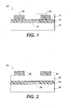
- FIG. 1 there is schematically illustrated a TFT configuration 10 comprised of a substrate 16, in contact therewith a metal contact 18 (gate electrode), and a layer of an insulating dielectric layer 14 with the gate electrode having a portion thereof or the entire gate in contact with the dielectric layer 14 on top of which layer 14 two metal contacts, 20 and 22 (source and drain electrodes), are deposited.
- a metal contact 18 gate electrode
- a layer of an insulating dielectric layer 14 with the gate electrode having a portion thereof or the entire gate in contact with the dielectric layer 14 on top of which layer 14 two metal contacts, 20 and 22 (source and drain electrodes), are deposited.
- layer 12 comprised of the poly(dithienylbenzo[1,2-b:4,5-b']dithiophene) semiconductor, poly(4,8-didodecyl-2,6-bis-(3-methyl-thiophen-2-yl)-benzo[1,2-b;4,5-b']dithiophene), of Formula (22) wherein n is 23, or poly(4,8-dihexyl-2,6-bis-(3-hexyl-thiophen-2-yl)-benzo[1,2-b:4,5-b']dithiophene), of Formula (23), where n is 24.
- the gate electrode can be included in the substrate, in the dielectric layer, and the like throughout.
- FIG. 2 schematically illustrates another TFT configuration 30 comprised of a substrate 36, a gate electrode 38, a source electrode 40, and a drain electrode 42, an insulating dielectric layer 34, and the semiconductor layer 32 of poly(4,8-didodecyl-2,6-bis-(3-methyl-thiophen-2-yl)-benzo[1,2-b;4,5-b']dithiophene) of Formula (22), or poly(4,8-dihexyl-2,6-bis-(3-hexyl-thiophen-2-yl)-benzo[1,2-b:4,5-b']dithiophene) (23).
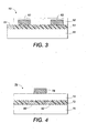
- FIG. 3 schematically illustrates a further TFT configuration 50 comprised of a heavily n-doped silicon wafer 56, which can act as a gate electrode, a thermally grown silicon oxide dielectric layer 54, the poly(dithienylbenzo[1,2-b:4,5-b']dithiophene) semiconductor layer 52 of poly(4,8-didodecyl-2,6-bis-(3-methyl-thiophen-2-yl)-benzo[1,2-b;4,5-b']dithiophene) (22), or poly(4,8-dihexyl-2,6-bis-(3-hexyl-thiophen-2-yl)-benzo[1,2-b:4,5-b']dithiophene) (23), and a source electrode 60, a drain electrode 62; and a gate electrode contact 64.
- a heavily n-doped silicon wafer 56 which can act as a gate electrode
- a thermally grown silicon oxide dielectric layer 54 the poly
- FIG. 4 schematically illustrates a TFT configuration 70 comprised of substrate 76, a gate electrode 7 8, a source electrode 80, a drain electrode 82, p - type semiconductors of the formulas as illustrated herein semiconductor layer 72 of poly(4,8-didodecyl-2,6-bis-(3-methyl-thiophen-2-yl)-benzo[1,2-b;4,5-b']dithiophene) of Formula (22), wherein n is 23, or poly(4,8-dihexyl-2,6-bis-(3-hexyl-thiophen-2-yl)-benzo[1,2-b:4,5-b']dithiophene) (23), wherein n is 24, and an insulating dielectric layer 74.
- an optional protecting layer may be incorporated on top of each of the transistor configurations of Figures 1, 2 , 3 and 4 .
- the insulating dielectric layer 74 may also function as a protecting layer.
- the substrate layer may generally be a silicon material inclusive of various appropriate forms of silicon, a glass plate, a plastic film or a sheet, and the like depending on the intended applications.
- a plastic substrate such as for example polyester, polycarbonate, polyimide sheets, and the like, may be selected.
- the thickness of the substrate may be, for example, from about 10 micrometers to over 10 millimeters with a specific thickness being from about 50 to about 100 micrometers, especially for a flexible plastic substrate, and from about 1 to about 10 millimeters for a rigid substrate such as glass or silicon.
- the insulating dielectric layer which can separate the gate electrode from the source and drain elec trodes, and in contact with the semiconductor layer, can generally be an inorganic material film, an organic polymer film, or an organic - inorganic composite film.
- the thickness of the dielectric layer is, for example, from about 10 nanometers to about 1 micrometer with a more specific thickness being about 100 nanometers to about 500 nanometers.
- Illustrative examples of inorganic materials suitable as the dielectric layer include silicon oxide, silicon nitride, aluminum oxide, barium titanate, barium zirc onate titanate, and the like; illustrative examples of organic polymers for the dielectric layer include polyesters, polycarbonates, poly(vinyl phenol), polyimides, polystyrene, poly(methacrylate)s, poly(acrylate)s, epoxy resin, and the like; and illustrat ive examples of inorganic-organic composite materials include nanosized metal oxide particles dispersed in polymers, such as polyester, polyimide, epoxy resin, and the like.
- the insulating dielectric layer is generally of a thickness of from about 50 nano meters to about 500 nanometers depending on the dielectric constant of the dielectric material used. More specifically, the dielectric material has a dielectric constant of, for example, at least about 3, thus a suitable dielectric thickness of about 300 nanometers can provide a desirable capacitance, for example, of about 10 -9 to about 10 -7 F/cm 2 .
- the active semiconductor layer comprised of p -type semiconductors of the formulas as illustrated herein, and wherein the thickness of this layer is generally, for example, about 10 nanometers to about 1 micrometer, or about 40 to about 100 nanometers.
- This layer can generally be fabricated by solution processes such as spin coating, casting, screen, stamp, or jet printing of a solution of p-type semiconductors of the present disclosure.
- the gate electrode can be a thin metal film, a conducting polymer film, a conducting film generated from a conducting ink o r paste, or the substrate itself (for example heavily doped silicon).
- gate electrode materials include, but are not limited to aluminum, gold, chromium, indium tin oxide, conducting polymers, such as polystyrene sulfonate -doped poly(3,4-ethylenedioxythiophene) (PSS/PEDOT), a conducting ink/paste comprised of carbon black/graphite or colloidal silver dispersion contained in a polymer binder, such as Electrodag available from Acheson Colloids Company, and silver filled electrically conductive thermoplastic ink available from Noelle Industries, and the like.
- the gate layer can be prepared by vacuum evaporation, sputtering of metals or conductive metal oxides, coating from conducting polymer solutions or conducting inks, or dispersions by spin coat ing, casting or printing.
- the thickness of the gate electrode layer is, for example, from about 10 nanometers to about 10 micrometers, and a specific thickness is, for example, from about 10 to about 200 nanometers for metal films, and about 1 to about 10 micrometers for polymer conductors.
- the source and drain electrode layer can be fabricated from materials which provide a low resistance ohmic contact to the semiconductor layer.
- Typical materials suitable for use as source and drain electrodes include those of the gate electrode materials such as gold, nickel, aluminum, platinum, conducting polymers, and conducting inks.
- Typical thickness of this layer is, for example, from about 40 nanometers to about 1 micrometer with the more specific thickness bein g about 100 to about 400 nanometers.
- the TFT devices contain a semiconductor channel with a width W and length L.
- the semiconductor channel width may be, for example, from about 10 micrometers to about 5 millimeters with a specific channel width being about 100 micrometers to about 1 millimeter.
- the semiconductor channel length may be, for example, from about 1 micrometer to about 1 millimeter with a more specific channel length being from about 5 micrometers to about 100 micrometers.
- the source electrode is grounded and a bias voltage of generally, for example, about 0 volt to about -80 volts is applied to the drain electrode to collect the charge carriers transported across the semiconductor channel when a voltage of generally, for example, about +10 volts to about -80 volts is applied to the gate electrode.
- the test device was comprised of an n-doped silicon wafer with a thermally grown silicon ox ide layer of a thickness of about 200 nanometers thereon.
- the wafer functioned as the gate electrode while the silicon oxide layer acted as the gate dielectric; the silicon oxide layer had a capacitance of about 15 nF/cm 2 (nanofarads/square centimeter) as measured with a capacitor meter.
- the silicon wafer was first cleaned with isopropanol, argon plasma, isopropanol and air dried.
- the solution was first filtrated through a 1 micrometer syringe filter, and then spin -coated onto the OTS8-treated silicon substrate at 1,000 rpm for 120 seconds in a warm atmosphere resulting in thin film with a thickness of a bout 20 to about 50 nanometers.
- gold source and drain electrodes of about 50 nanometers in thickness for each were deposited on top of the semiconductor layer by vacuum deposition through a shado w mask with various channel lengths and widths, thus creating a series of transistors of various dimensions.
- the evaluation of field-effect transistor devices performance was accomplished in a black box (that is, a closed box which excluded ambient light) at ambient conditions using a Keithley 4200 SCS semiconductor characterization system.
- the carrier mobility, ⁇ was calculated from the data in the saturated regime (gate voltage, V G ⁇ source-drain voltage, V SD ) according to equation (1)
- I SD C i ⁇ W / 2 ⁇ L ⁇ V G ⁇ V T 2
- I SD is the drain current at the saturated regime
- W and L are, respectively, the semiconductor channel width and length
- C i is the capacitance per unit area of the gate dielectric layer
- V G and V T are, respectively, the gate volt age and threshold voltage.
- Another property of field-effect transistor is its current on/off ratio. This is the ratio of the saturation source-drain current at the accumulation regime to the source-drain current at the depletion regime.
- a 100 milliliter three-necked round-bottomed flask was charged with magnetic stirrer, adding funnel and water condenser, and flushed with Argon and vacuumed three times at heating. Milligram turnings (0.83 gram, 34 .0 mmol) were added into the flask and the system was flushed with Argon for 10 minutes before 10 milliliters of anhydrous ether were added. 2 -bromo-3-hexyl-thiophene (7 grams, 28.3 mmol) with 20 milliliters anhydrous ether was added into the adding funne I. Around 5 milliliters of a thiophene solution were dropped slowly into the flask and heated the flask a little bit with heat gun.
- the reaction started three minutes late with continuous bubbling of ether, and the thiophene solution was dropped into the flask and the reaction was stirred at room temperature for another 2 hours.
- the Grignard solution was transferred to another 100 milliliter two -necked flask, and then cooled the solution to -78°C. A white precipitate formed when cooled and the solution became viscous.
- 2-Isopropoxy-4,4,5,5-tetramethyl-1,3,2-dioxaborolane (7 milliliters, 34 mmol) was added through syringe at -78°C. The precipitates were dissolved during the adding. Then the solution was warmed to room temperature and stirred for a furth er 18 hours.
- a dark red solid g was obtained after filtration, which was purified by Soxhlet extraction with methanol for 4 hours, and heptane for 24 hours. Then chlorobenzene was used to extract polymer for 16 hours. Removal of solvent and drying in vacuo provided 60 milligrams (12 percent yield) of brown powder.
- the test device was comprised of an n-doped silicon wafer with a thermally grown silicon oxide layer of a thickness of about 200 nanometers thereon.
- the wafer functioned as the gate electrode while the silicon oxide layer acted as the gate dielectric; the silicon oxide layer had a capacitance of about 15 nF/cm 2 (nanofarads/square centimeter) as measured with a capacitor meter.
- the silicon wafer was first cleaned with isopropanol, argon plasma, isopropanol and air dried.
- the solution was first filtrated through a 1 micrometer syringe filter, and then spin -coated onto the OTS8-treated silicon substrate at 1,000 rpm for 120 seconds in w arm atmosphere, resulting in thin film with a thickness of about 20 to about 50 nanometers.
- gold source and drain electrodes of about 50 nanometers in thickness for each were deposited on top of the semiconductor layer by vacuum deposition through a shadow mask with various channel lengths and widths, thus creating a series of transistors of various dimensions.
- the evaluation of field-effect thin film transistor performance was accomplished in a b lack box (that is, a closed box which excluded ambient light) at ambient conditions using a Keithley 4200 SCS semiconductor characterization system.
- Another property of field -effect transistor was its current on/off ratio. This was the ratio of the saturation source -drain current at the accumulation regime to the source-drain current at the depletion regime.
- thin film transistor of poly(dithienylbenzo[1,2-b:4,5-b']dithiophene)s encompassed by Formulas/Structures (I) was excellent semiconductors for electronic devices.
- the device fabrication and characterization were accomplished in ambient conditions, evidencing their oxidative stability for a number of weeks as compared to regioregular poly(3-alkylthiophene)s devices which were stable for about less than one week.
Landscapes
- Chemical & Material Sciences (AREA)
- Organic Chemistry (AREA)
- Engineering & Computer Science (AREA)
- Materials Engineering (AREA)
- Health & Medical Sciences (AREA)
- Chemical Kinetics & Catalysis (AREA)
- Medicinal Chemistry (AREA)
- Polymers & Plastics (AREA)
- Thin Film Transistor (AREA)
- Polyoxymethylene Polymers And Polymers With Carbon-To-Carbon Bonds (AREA)
Applications Claiming Priority (2)
| Application Number | Priority Date | Filing Date | Title |
|---|---|---|---|
| US11/586,449 US7834132B2 (en) | 2006-10-25 | 2006-10-25 | Electronic devices |
| US11/586,448 US7820782B2 (en) | 2006-10-25 | 2006-10-25 | Poly(dithienylbenzo[1,2-b:4,5-b′]dithiophene) polymers |
Publications (2)
| Publication Number | Publication Date |
|---|---|
| EP1916250A1 EP1916250A1 (en) | 2008-04-30 |
| EP1916250B1 true EP1916250B1 (en) | 2011-01-05 |
Family
ID=38926331
Family Applications (1)
| Application Number | Title | Priority Date | Filing Date |
|---|---|---|---|
| EP07119190A Active EP1916250B1 (en) | 2006-10-25 | 2007-10-24 | Electronic devices comprising poly(dithienyl-benzodithiophenes) as semiconductors |
Country Status (7)
| Country | Link |
|---|---|
| EP (1) | EP1916250B1 (ja) |
| JP (1) | JP5472874B2 (ja) |
| KR (1) | KR101397662B1 (ja) |
| BR (1) | BRPI0703903A (ja) |
| CA (1) | CA2606985C (ja) |
| DE (1) | DE602007011709D1 (ja) |
| TW (1) | TW200834572A (ja) |
Cited By (2)
| Publication number | Priority date | Publication date | Assignee | Title |
|---|---|---|---|---|
| KR101561323B1 (ko) | 2008-07-02 | 2015-10-16 | 바스프 에스이 | 폴리(5,5'-비스(티오펜-2-일)-벤조[2,1-b;3,4-b']디티오펜) 및 이의 고성능 용액 가공가능한 반전도성 중합체로서의 용도 |
| KR101763954B1 (ko) | 2009-05-21 | 2017-08-01 | 라이너지 테크 인코포레이션 | 공액 중합체 및 광전자 장치에서 이의 용도 |
Families Citing this family (20)
| Publication number | Priority date | Publication date | Assignee | Title |
|---|---|---|---|---|
| US20090181509A1 (en) * | 2008-01-14 | 2009-07-16 | Xerox Corporation | Polymer semiconductors with high mobility |
| JP2009215546A (ja) * | 2008-02-13 | 2009-09-24 | Sumitomo Chemical Co Ltd | 多環縮環化合物、多環縮環重合体及びこれらを含む有機薄膜 |
| US7968871B2 (en) * | 2008-04-11 | 2011-06-28 | Xerox Corporation | Organic thin film transistor |
| US8367798B2 (en) * | 2008-09-29 | 2013-02-05 | The Regents Of The University Of California | Active materials for photoelectric devices and devices that use the materials |
| KR101780083B1 (ko) * | 2009-12-02 | 2017-10-10 | 바스프 에스이 | 디티에노벤조-티에노[3,2-b]티오펜 공중합체 및 고성능 용액 공정 가능한 반도체 중합체로서 이의 용도 |
| US10050201B2 (en) * | 2010-04-19 | 2018-08-14 | Merck Patent Gmbh | Polymers of benzodithiophene and their use as organic semiconductors |
| US8895693B2 (en) | 2010-06-25 | 2014-11-25 | Samsung Electronics Co., Ltd. | Electron-donating polymers and organic solar cells including the same |
| KR101792901B1 (ko) | 2010-07-09 | 2017-11-02 | 메르크 파텐트 게엠베하 | 반도전성 중합체 |
| DE102010032737A1 (de) | 2010-07-29 | 2012-02-02 | Merck Patent Gmbh | Polymere enthaltend substituierte Benzodithiopheneinheiten, Blends enthaltend diese Polymere sowie Vorrichtungen enthaltend diese Polymere oder Blends |
| US8759421B2 (en) * | 2010-08-31 | 2014-06-24 | Samsung Electronics Co., Ltd. | Continuous process for preparing nanodispersions using an ultrasonic flow-through heat exchanger |
| US9790236B2 (en) | 2011-01-05 | 2017-10-17 | Samsung Electronics Co., Ltd. | Organic semiconductor compound, and transistor and electronic device including the same |
| US20120168726A1 (en) * | 2011-01-05 | 2012-07-05 | Samsung Electronics Co., Ltd. | Organic semiconductor compound, and transistor and electronic device including the same |
| US8394918B2 (en) | 2011-02-28 | 2013-03-12 | Corning Incorporated | Five-ring fused heteroaromatic compounds and conjugated polymers thereof |
| WO2012129511A2 (en) * | 2011-03-24 | 2012-09-27 | Northwestern University | Semiconducting compounds and devices incorporating same |
| KR101853395B1 (ko) | 2011-05-23 | 2018-04-30 | 삼성전자주식회사 | 전자 공여체 고분자 및 이를 포함하는 태양 전지 |
| JP2014531493A (ja) * | 2011-09-23 | 2014-11-27 | オーシャンズ キング ライティング サイエンスアンドテクノロジー カンパニー リミテッド | ジフルオロベンゾトリアゾリル太陽電池ポリマー材料、並びにその調製方法及び使用 |
| US9590178B2 (en) | 2011-09-28 | 2017-03-07 | Merck Patent Gmbh | Conjugated polymers |
| KR101777326B1 (ko) | 2011-10-05 | 2017-09-12 | 삼성전자주식회사 | 전자 공여체 고분자 및 이를 포함하는 유기 태양 전지 |
| CN104781367B (zh) * | 2012-11-07 | 2017-04-26 | 巴斯夫欧洲公司 | 基于萘并二酮的聚合物 |
| EP2928940B1 (en) * | 2012-12-04 | 2021-03-03 | CLAP Co., Ltd. | Functionalized benzodithiophene polymers for electronic application |
Family Cites Families (3)
| Publication number | Priority date | Publication date | Assignee | Title |
|---|---|---|---|---|
| DE602004024629D1 (de) * | 2003-10-15 | 2010-01-28 | Merck Patent Gmbh | Polybenzodithiophene |
| JP2005206750A (ja) * | 2004-01-26 | 2005-08-04 | Konica Minolta Holdings Inc | 有機半導体材料、有機トランジスタ、電界効果トランジスタ、スイッチング素子及び5員複素環化合物 |
| CN100443483C (zh) * | 2005-12-08 | 2008-12-17 | 中国科学院长春应用化学研究所 | 稠环单元封端的齐聚噻吩类高迁移率有机半导体材料及用途 |
-
2007
- 2007-10-18 CA CA2606985A patent/CA2606985C/en not_active Expired - Fee Related
- 2007-10-18 JP JP2007271009A patent/JP5472874B2/ja active Active
- 2007-10-24 DE DE602007011709T patent/DE602007011709D1/de active Active
- 2007-10-24 TW TW096139790A patent/TW200834572A/zh unknown
- 2007-10-24 EP EP07119190A patent/EP1916250B1/en active Active
- 2007-10-25 KR KR1020070107920A patent/KR101397662B1/ko active IP Right Grant
- 2007-10-25 BR BRPI0703903-4A patent/BRPI0703903A/pt not_active IP Right Cessation
Cited By (2)
| Publication number | Priority date | Publication date | Assignee | Title |
|---|---|---|---|---|
| KR101561323B1 (ko) | 2008-07-02 | 2015-10-16 | 바스프 에스이 | 폴리(5,5'-비스(티오펜-2-일)-벤조[2,1-b;3,4-b']디티오펜) 및 이의 고성능 용액 가공가능한 반전도성 중합체로서의 용도 |
| KR101763954B1 (ko) | 2009-05-21 | 2017-08-01 | 라이너지 테크 인코포레이션 | 공액 중합체 및 광전자 장치에서 이의 용도 |
Also Published As
| Publication number | Publication date |
|---|---|
| CA2606985A1 (en) | 2008-04-25 |
| JP2008109135A (ja) | 2008-05-08 |
| KR20080037580A (ko) | 2008-04-30 |
| CA2606985C (en) | 2011-02-01 |
| TW200834572A (en) | 2008-08-16 |
| JP5472874B2 (ja) | 2014-04-16 |
| DE602007011709D1 (de) | 2011-02-17 |
| KR101397662B1 (ko) | 2014-06-27 |
| EP1916250A1 (en) | 2008-04-30 |
| BRPI0703903A (pt) | 2008-06-10 |
Similar Documents
| Publication | Publication Date | Title |
|---|---|---|
| EP1916250B1 (en) | Electronic devices comprising poly(dithienyl-benzodithiophenes) as semiconductors | |
| US7820782B2 (en) | Poly(dithienylbenzo[1,2-b:4,5-b′]dithiophene) polymers | |
| US7834132B2 (en) | Electronic devices | |
| EP1679330B1 (en) | Polythiophenes and devices thereof | |
| EP1327647B1 (en) | Polythiophenes and devices thereof | |
| US6770904B2 (en) | Polythiophenes and electronic devices generated therefrom | |
| EP1329474B1 (en) | Polythiophenes and devices thereof | |
| EP1329477B1 (en) | Polythiophenes and devices thereof | |
| US7250625B2 (en) | Polythiophenes and electronic devices generated therefrom | |
| EP1329476B1 (en) | Polythiophenes and devices thereof | |
| EP1605007B1 (en) | Processes to prepare oligomeric thiophene compounds | |
| EP2213692A1 (en) | Polymer Semiconductors with High Mobility | |
| US7049629B2 (en) | Semiconductor polymers and devices thereof | |
| EP1843409B1 (en) | Organic thin film transistor comprising a poly(ethynylthiophene) | |
| US20040183068A1 (en) | Fluorinated polythiophenes and devices thereof | |
| US20040186266A1 (en) | Fluorinated polythiophenes and devices thereof | |
| US20070093641A1 (en) | Polymers | |
| US20090242878A1 (en) | Optimization of new polymer semiconductors for better mobility and processibality | |
| US20070238852A1 (en) | Poly(alkynylthiophenes)s |
Legal Events
| Date | Code | Title | Description |
|---|---|---|---|
| PUAI | Public reference made under article 153(3) epc to a published international application that has entered the european phase |
Free format text: ORIGINAL CODE: 0009012 |
|
| AK | Designated contracting states |
Kind code of ref document: A1 Designated state(s): AT BE BG CH CY CZ DE DK EE ES FI FR GB GR HU IE IS IT LI LT LU LV MC MT NL PL PT RO SE SI SK TR |
|
| AX | Request for extension of the european patent |
Extension state: AL BA HR MK RS |
|
| RIN1 | Information on inventor provided before grant (corrected) |
Inventor name: PAN, HUALONG Inventor name: ONG, BENG S. Inventor name: LI, YUNING Inventor name: LIU, PING Inventor name: WU, YILIANG |
|
| 17P | Request for examination filed |
Effective date: 20081030 |
|
| 17Q | First examination report despatched |
Effective date: 20081125 |
|
| AKX | Designation fees paid |
Designated state(s): DE FR GB |
|
| GRAP | Despatch of communication of intention to grant a patent |
Free format text: ORIGINAL CODE: EPIDOSNIGR1 |
|
| GRAS | Grant fee paid |
Free format text: ORIGINAL CODE: EPIDOSNIGR3 |
|
| GRAA | (expected) grant |
Free format text: ORIGINAL CODE: 0009210 |
|
| AK | Designated contracting states |
Kind code of ref document: B1 Designated state(s): DE FR GB |
|
| REG | Reference to a national code |
Ref country code: GB Ref legal event code: FG4D |
|
| REF | Corresponds to: |
Ref document number: 602007011709 Country of ref document: DE Date of ref document: 20110217 Kind code of ref document: P |
|
| REG | Reference to a national code |
Ref country code: DE Ref legal event code: R096 Ref document number: 602007011709 Country of ref document: DE Effective date: 20110217 |
|
| PLBE | No opposition filed within time limit |
Free format text: ORIGINAL CODE: 0009261 |
|
| STAA | Information on the status of an ep patent application or granted ep patent |
Free format text: STATUS: NO OPPOSITION FILED WITHIN TIME LIMIT |
|
| 26N | No opposition filed |
Effective date: 20111006 |
|
| REG | Reference to a national code |
Ref country code: DE Ref legal event code: R097 Ref document number: 602007011709 Country of ref document: DE Effective date: 20111006 |
|
| REG | Reference to a national code |
Ref country code: DE Ref legal event code: R081 Ref document number: 602007011709 Country of ref document: DE Owner name: SAMSUNG ELECTRONICS CO., LTD., KR Free format text: FORMER OWNER: XEROX CORP., ROCHESTER, US Effective date: 20130820 Ref country code: DE Ref legal event code: R081 Ref document number: 602007011709 Country of ref document: DE Owner name: SAMSUNG ELECTRONICS CO., LTD., SUWON-SI, KR Free format text: FORMER OWNER: XEROX CORP., ROCHESTER, NEW YORK, US Effective date: 20130820 |
|
| REG | Reference to a national code |
Ref country code: FR Ref legal event code: TP Owner name: SAMSUNG ELECTRONICS CO., LTD., KR Effective date: 20131105 |
|
| REG | Reference to a national code |
Ref country code: GB Ref legal event code: 732E Free format text: REGISTERED BETWEEN 20140306 AND 20140312 |
|
| REG | Reference to a national code |
Ref country code: FR Ref legal event code: PLFP Year of fee payment: 10 |
|
| REG | Reference to a national code |
Ref country code: FR Ref legal event code: PLFP Year of fee payment: 11 |
|
| REG | Reference to a national code |
Ref country code: FR Ref legal event code: PLFP Year of fee payment: 12 |
|
| PGFP | Annual fee paid to national office [announced via postgrant information from national office to epo] |
Ref country code: GB Payment date: 20230914 Year of fee payment: 17 |
|
| PGFP | Annual fee paid to national office [announced via postgrant information from national office to epo] |
Ref country code: FR Payment date: 20230921 Year of fee payment: 17 |
|
| PGFP | Annual fee paid to national office [announced via postgrant information from national office to epo] |
Ref country code: DE Payment date: 20230919 Year of fee payment: 17 |