EP1914757A2 - Dispositif et procédé de stockage - Google Patents
Dispositif et procédé de stockage Download PDFInfo
- Publication number
- EP1914757A2 EP1914757A2 EP07251753A EP07251753A EP1914757A2 EP 1914757 A2 EP1914757 A2 EP 1914757A2 EP 07251753 A EP07251753 A EP 07251753A EP 07251753 A EP07251753 A EP 07251753A EP 1914757 A2 EP1914757 A2 EP 1914757A2
- Authority
- EP
- European Patent Office
- Prior art keywords
- memory device
- unit
- semiconductor memory
- writing
- functional capacity
- Prior art date
- Legal status (The legal status is an assumption and is not a legal conclusion. Google has not performed a legal analysis and makes no representation as to the accuracy of the status listed.)
- Withdrawn
Links
Images


Classifications
-
- G—PHYSICS
- G11—INFORMATION STORAGE
- G11C—STATIC STORES
- G11C29/00—Checking stores for correct operation ; Subsequent repair; Testing stores during standby or offline operation
- G11C29/70—Masking faults in memories by using spares or by reconfiguring
- G11C29/76—Masking faults in memories by using spares or by reconfiguring using address translation or modifications
- G11C29/765—Masking faults in memories by using spares or by reconfiguring using address translation or modifications in solid state disks
-
- G—PHYSICS
- G06—COMPUTING; CALCULATING OR COUNTING
- G06F—ELECTRIC DIGITAL DATA PROCESSING
- G06F3/00—Input arrangements for transferring data to be processed into a form capable of being handled by the computer; Output arrangements for transferring data from processing unit to output unit, e.g. interface arrangements
- G06F3/06—Digital input from, or digital output to, record carriers, e.g. RAID, emulated record carriers or networked record carriers
- G06F3/0601—Interfaces specially adapted for storage systems
- G06F3/0602—Interfaces specially adapted for storage systems specifically adapted to achieve a particular effect
- G06F3/0614—Improving the reliability of storage systems
- G06F3/0616—Improving the reliability of storage systems in relation to life time, e.g. increasing Mean Time Between Failures [MTBF]
-
- G—PHYSICS
- G06—COMPUTING; CALCULATING OR COUNTING
- G06F—ELECTRIC DIGITAL DATA PROCESSING
- G06F3/00—Input arrangements for transferring data to be processed into a form capable of being handled by the computer; Output arrangements for transferring data from processing unit to output unit, e.g. interface arrangements
- G06F3/06—Digital input from, or digital output to, record carriers, e.g. RAID, emulated record carriers or networked record carriers
- G06F3/0601—Interfaces specially adapted for storage systems
- G06F3/0628—Interfaces specially adapted for storage systems making use of a particular technique
- G06F3/0638—Organizing or formatting or addressing of data
- G06F3/064—Management of blocks
-
- G—PHYSICS
- G06—COMPUTING; CALCULATING OR COUNTING
- G06F—ELECTRIC DIGITAL DATA PROCESSING
- G06F3/00—Input arrangements for transferring data to be processed into a form capable of being handled by the computer; Output arrangements for transferring data from processing unit to output unit, e.g. interface arrangements
- G06F3/06—Digital input from, or digital output to, record carriers, e.g. RAID, emulated record carriers or networked record carriers
- G06F3/0601—Interfaces specially adapted for storage systems
- G06F3/0668—Interfaces specially adapted for storage systems adopting a particular infrastructure
- G06F3/0671—In-line storage system
- G06F3/0683—Plurality of storage devices
- G06F3/0688—Non-volatile semiconductor memory arrays
-
- G—PHYSICS
- G11—INFORMATION STORAGE
- G11C—STATIC STORES
- G11C16/00—Erasable programmable read-only memories
- G11C16/02—Erasable programmable read-only memories electrically programmable
- G11C16/06—Auxiliary circuits, e.g. for writing into memory
- G11C16/34—Determination of programming status, e.g. threshold voltage, overprogramming or underprogramming, retention
- G11C16/349—Arrangements for evaluating degradation, retention or wearout, e.g. by counting erase cycles
- G11C16/3495—Circuits or methods to detect or delay wearout of nonvolatile EPROM or EEPROM memory devices, e.g. by counting numbers of erase or reprogram cycles, by using multiple memory areas serially or cyclically
-
- G—PHYSICS
- G11—INFORMATION STORAGE
- G11C—STATIC STORES
- G11C29/00—Checking stores for correct operation ; Subsequent repair; Testing stores during standby or offline operation
- G11C29/70—Masking faults in memories by using spares or by reconfiguring
- G11C29/76—Masking faults in memories by using spares or by reconfiguring using address translation or modifications
Definitions
- the present invention relates to a storage device and a storing method, and more specifically, to a controlling method and an implementing method of a flash memory for enhancing reliability of a storing system using a flash memory.
- non-volatile semiconductor memory there is a flash memory for which a deletion unit or a writing unit (functional capacity unit) is previously determined.
- the flash memory has a floating gate structure, which wraps a conductor such as a polysilicon in an oxide insulator such as an oxide silicon for storing information by the presence of the charge, which is in the floating gate.
- the flash memory may use a structure for reserving a charge in a particular place other than the floating gate structure.
- the flash memory has a lifetime, with limited number of deletion and limited number of rewriting for each capacity of deletion unit.
- a method for prolonging the lifetime of non-volatile semiconductor memory with a lifetime for each deletion unit capacity includes a method for evening up the number of deletion for each deletion unit over the entire chip and a method for enabling the non-volatile semiconductor memory to keep operating as a memory device without a problem even if some deletion units cannot be used by providing a substitute region for substituting the part of the deletion units whose lifetime has expired.
- the methods can prolong the lifetime, however, cannot eliminate the lifetime.
- the flash memory has a lifetime and it dies if the lifetime has expired.
- a storage system using a flash memory needs a mechanism for compensating a part of the flash memory whose lifetime has expired even when the lifetime has expired in that part. At that moment, a failure occurs that a part of the flash memory is impossible to be deleted or written. In such a case, new data merely cannot be written in the part and already stored data can be read out without any problem. Therefore, it is effective to substituting only a part, in which deleting or writing is impossible, with another means leaving the remainder kept being used.
- the management of the logical address and the physical address is performed by the superior system, there is a problem in that the management table becomes too large, raising an implementing cost for a required memory or the like. There is a problem in that it takes much time in converting the logical address and the physical address and the performance is lowered when it is attempted to reduce the cost.
- the method has a problem in that it is ineffective to exchange a memory device when only a part of the memory device has become unavailable.
- the present invention is adapted, when one deletion unit in the flash drive or the like has a failure, to cause another flash drive to substitute the deletion unit.
- the present invention is preferably adapted to cause the superior controlling unit to mange which logical address is mapped for each deletion unit, i.e., to manage association between the logical address and the physical address.
- the present invention is preferably adapted to transfer the logical address to the flash drive without managing association between the logical address and the physical address in the superior controlling unit, cause each flash drive to determine whether data corresponding to the logical address is stored or not and return the result, and output the data.
- the present invention is preferably adapted to inquire the logical address for all the flash drives, which makes up the RAID group, in the system for improving reliability of data by integrating a plurality of flash drives such as RAID.
- the present invention is preferably adapted to set a range for logical addresses to be served for each RAID group and the logical addresses in a served range are inquired in parallel for each of different RAID groups.
- the present invention is preferably adapted to return information on whether a writing request from the superior controlling unit can be addressed or not to the superior controlling unit when data is written, cause the superior controlling unit to form a RAID parity group from a flash drive that can answer the writing request and write data.
- the present invention is preferably adapted to cause each flash drive among the flash drive forming a parity group to store data order and parity data classifying information instructed by the superior controlling unit by logical address unit as the flash drives forming a parity group differ for each logical address.
- the present invention is preferably adapted to cause the flash drive to save information indicating invalidity of the stored data, if the flash dive cannot address a writing request but a writing request is given from the superior controlling unit and the data corresponding to the logical address is stored.
- the present invention is preferably adapted to cause the flash drive to inform the superior controlling unit on the maximum value of the number of deletion of a deletion unit, and cause the superior controlling unit to issue a request to add a flash drive to the RAID group including the flash drive to an administrator, when the number of deletion reaches a predetermined number of times.
- the present invention may be adapted to add a flash module of a print substrate structure in which a flash memory is provided for the flash drive whose maximum number of deletion reaches a predetermined number of times to the flash drive so that the substituting region in the flash drive can be added.
- the least number of flash drives start to operate at first, and when the number of deletion reaches a predetermined number of times, a new flash drive is added for substituting the deletion unit the original flash drive whose lifetime has expired.
- Data is gradually transferred to a flash drive, to which substitutions are added, with valid data among data stored in the original flash drive decreasing.
- the present invention is preferably adapted to transfer the valid data in the flash drive to the added drive and remove the flash drive, when a predetermined threshold is exceeded.
- the present invention may be adapted to remove the flash drive and that on the removed flash drive is restored on the added drive by using the redundancy of the RAID, when the predetermined threshold is exceeded.
- the present invention may be adapted to enable the flash drives by twice the number of the minimum number of the flash drives, which form the RAID, to be connected in a RAID group.
- a capacity of the entire storage device can be kept by adding a flash drive or a flash module in the flash drive for a flash memory that has a failure.
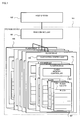
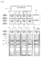
- FIG. 1 shows a configuration of a storage device 101 of the embodiment.
- the storage device 101 includes a plurality of flash drives 104 and a RAID controller 103, which controls the plurality of flash drives 104 in the storage device 101.
- the storage device 101 is connected to a host system 102 via the RAID controller 103.
- the flash drive 104 includes a plurality of flash modules 105, each of which is a printed board provided with a plurality of flash memory devices 107 and a flash memory controller 108.
- a flash drive controller 106 interfaces exchanges between the flash module 105 and the RAID controller 103, the superior controlling unit of the flash module 105.
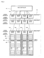
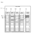
- the storage device 101 that puts much stress on reliability has a plurality of flash drives 104, for example, with four flash drives forming a RAID group 201.
- the RAID controller 103 allocates a logical address to a unit of the RAID group 201.
- the flash drive 104 includes a plurality of flash modules 105. Each flash module includes multiple flash memory devises 107.
- a flash memory device 202 includes a deletion unit 203, which is called a block, and a writing unit 204, which is called a page.
- the writing unit 204 corresponds to a sector as it is called in an HDD but the writing unit 204 may be formed with a plurality of sectors.
- the RAID controller 103 forms the RAID group 201 with four flash drives 104 and manages a plurality of RAID group.
- a logical address is allocated to each of the RAID groups according to a capacity of the RAID group.
- the logical address corresponds to a logical address given by the superior host system 102.
- a writing unit 204 with a deletion unit 203 in a flash memory chip 202 corresponding to the logical address is selected from each flash drive 104 to form a parity group 205 by four writing units.
- the RAID controller reads data by a parity group unit 205.
- each data is managed by a logical address.
- the logical addresses are converted into an address of a specific drive, an address of a specific flash memory chip, an address of a specific deletion unit in a chip, and an address of a specific writing unit by the RAID controller or the flash drive controller.
- a flash memory is limited in the number of times todelete/rewrite. If the flash memory has a great number of pieces of valid data, the deleted deletion unit that can be written decreases to be finally eliminated. In such state, it can address reading but hard to address writing.
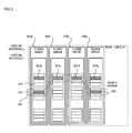
- a flash drive 601 is added to flash drives 104b, c, d and e forming a RAID group as shown in FIG. 6 so that the flash drive 601 can substitute for the flash drive which can no longer address writing.
- the substituting is only for writing data, and the originally included flash drive is used for reading data that has not been updated. For example, such an operation is taken; if writing to the flash drive 104e cannot be addressed in the parity group 602, data for the flash drive 104e is written into the flash drive 601; and if writing to the flash drive 104d cannot be addressed in the parity group 603, data for the flash drive 104d is written into the flash drive 601.
- That operation has an effect in prolonging the lifetime of the entire external storage device only by adding a new flash drive to the RAID group after the four flash drives began to operate at the beginning of the operation and before any of the flash drives becomes to be unable to address writing so that the new flash drive substitutes for writing to the flash drive that is unable to address the writing to keep the capacity of the external storage device.
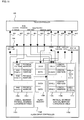
- the flash drive 104 and the RAID controller 103 are interfaced by a logical address 902, a data owning signal 907, a writing enabled signal 901, a writing request 904, a nullification request 905, a data input 906, a RAID position 908 for performing data identification in a parity group of read out data, a RAID position 903 for performing data identification in a parity group in writing, and status information 910.
- the status information 901 includes information on the usage state of the flash memory such as the maximum number of times to delete a deletion unit and a ratio of the valid data.
- the signals and information may be respectively connected as independent signals or may take a form of a command and a response that are exchanged via a certain communication interface.
- the RAID controller 103 is provided with a switch mechanism 802 for selecting four drives from the drives that can be connected inside a RAID group and sorting the data as shown in FIG. 8.
- the logical address 401 sent from the host system 102 is conventionally converted into the drive address 403 and the logical address in a drive 404 by the RAID controller 103.
- the data 402 sent from the host system 102 is processed to four pieces of data of three pieces of writing units 407 and a piece of parity data 408.
- the four pieces of data are respectively stored in different flash drives as a rule.
- the drive address 403 and the logical address in a drive 404 can be obtained by calculation by using the logical address 401.
- a flash drive that has a deletion unit that reached the limited number of times to delete of the flash memory may substitute the writing to the other flash drives so that which flash drive has the writing unit corresponding to the logical address therein needs to be managed.
- a superior RAID controller may manage it. In such a case, which flash drive is each writing unit present needs to be managed, requiring a large-scale conversion table.
- the RAID controller determines what superior to the logical address from the host system and examines which RAID group the data belongs to. The remaining logical address becomes a logical address inside the RAID group, which is sent to all the flash drives in the RAID group.
- Each flash drive determines whether it owns data corresponding to the received logical address or not and answers whether it owns the data or not to the RAID controller by an owning signal 907. If the flash drive actually owns the data, it outputs the corresponding data as read out data 909 and outputs which data is among the three pieces of data in the parity group and a parity by the RAID position 908.
- the RAID controller selects four flash drives which output owning signals from a plurality of flash derives inside the RAID group, checks respective RAID positions, sorts the pieces of data and restores the data.
- the fourth flash drive is restored by using a RAID function and the data is restored.
- the owning signals are obtained from five or more flash drives, old data in the same logical address and new data are included. Thus, if time and generation information are also managed, the data is restored by retrieving the latest data by using those pieces of data. If there is no time and generation information, the state is addressed as an error.
- the RAID controller If the RAID controller writes data, it selects four flash drives that can be written among a plurality of flash drives in a RAID group, transfers the logical address 902, the RAID position information 903 and the data 906, and writes them by using the writing request signals 904. To the unselected flash drives, the logical address 902 and the nullification signal 905 are transferred. If the flash drive receives the logical address 902 and the nullification signal 905 and owns data corresponding to the logical address 902, it nullifies the data. If the flash drive does not own data corresponding to the logical address 902, it ignores the logical address 902 and the nullification signal 905.
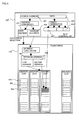
- the flash drive controller 106 has a table 1101 for converting a given logical address to an address of the writing unit in an actual flash memory chip (physical address) and a conversion table 1102 for converting a physical address to a logical address.
- a table for converting a logical address to a physical address stores RAID position information 1103 corresponding to a logical address and a physical address 1104.
- the conversion table has entries for writing unit capacity included in the flash drive.
- the flash drive controller 106 outputs a writing enabled signal 901 if the writing unit information-storing unit 1105 of a physical address logical address conversion table has space.
- the logical address 902 the RAID position information 903, the writing signal 904 and the writing data 906 are inputted.
- the flash drive controller 106 accesses the logical address physical address conversion table 1101 by using the inputted logical address as an entry, registers the inputted RAID position 1103, finds out a spaced writing unit from the physical address logical address conversion table 1102 and registers the physical address 1104.
- the RAID controller 103 inputs the logical address 902 in reading.
- the flash drive controller 106 accesses the logical address physical address conversion table 1101 by using the inputted logical address as an entry and checks whether an effective physical address 1104 is registered or not. If the effective physical address 1104 is registered, the flash drive controller 106 accesses the physical address logical address conversion table 1102, checks the writing unit information-storing unit 1105 indicating the valid/invalid/space of the data. If the data is valid, outputs the data owning signal 907, the RAID position information 908 and the data 910 of the writing unit 1109 of the flash memory 1108 corresponding to the physical address.
- nullification signal 905 is inputted instead of the writing signal 904 when the data is written, a physical address is obtained from the inputted logical address and the writing unit information-storing unit 1105 indicating the valid/invalid/space of the corresponding physical address logical address conversion table 1102 is nullified.
- the physical address logical address conversion table 1102 In the physical address logical address conversion table 1102, information 1107 on the number of times to delete is managed for each of the deletion unit, which is a set of a plurality of writing units, the maximum value inside the physical address logical address conversion table 1102 is examined and outputted as the status information 910.
- the flash memory 1108 is described in the figure, but it is not present in the flash drive controller 106.
- the figure describes the flash memory 1108 to schematically show correspondence with the physical address logical address conversion table and a flow of data.
- the physical address logical address conversion table may be present in the flash drive controller or may be realized by using a region in a part of the flash memory.
- the logical address physical address conversion table may also be present in the flash drive controller or may be realized by using a region in a part of the flash memory.
- the RAID controller updates or overwrites a part of the data forming a parity group, it reads data from the parity group, updates or overwrites a part of the data, generates the parity data and writes it again in the flash drive.
- the flash drive registers a physical address of the writing unit in a space state to the physical address of the logical address physical address conversion table 1101 and nullifies the writing unit information-storing unit 1105 of the previous physical address of the physical address logical address conversion table 1102.
- the flash drive Regularly or when the number of spaced writing units decreases to below a determined value, the flash drive examines the physical address logical address conversion table and finds out a deletion unit that has a high ratio of invalid writing units in a deletion unit. If an invalid state is more than a determined ratio, pieces of valid data in the deletion unit are transferred to a spaced writing unit one by one, all states of writing units in the original deletion unit are nullified and the deletion unit is deleted. At this moment, the transferred logical address of the writing units is checked and the logical address physical address conversion table is updated.
- any method can be taken for a RAID controller to select four flash drives from a RAID group, but the flash drives may be in prioritized. If a piece of data of a minimum unit is written, two parts of a corresponding data part and a parity in the corresponding parity group are updated and written in the corresponding flash drives. As a result, the number of times to rewrite a device of a deletion unit of the flash memory that forms a parity group is varied.
- a fault occurs such as unable to delete or unable to write for each deletion unit of the flash memory in the flash drive.
- Substitute regions are prepared in the flash module or the flash drive to some extent to address the fault.
- the flash drive may become unable to accept a writing request. This state can be predicted from information on the maximum number of times to delete. A method may be taken for adding a new flash drive to the RAID group when the maximum number of times to delete exceeds a predetermined value.
- the flash drive can be added by one unit. If two flash drives that forms the RAID group cannot address a writing request, two writing units of four writing units that forms the parity group are written in a flash drive. Thus, it is difficult to read out data of the parity group at a time so that normal performance as the RAID system cannot be exerted. Therefore, a method can be taken for deciding the number of flash drives to be added by monitoring the maximum number of times to delete of the flash drives in the RAID group and comparing the maximum number with a predetermined value.
- a ratio of valid data in the deletion unit is decreasing.
- a ratio of a valid data is also monitored. If the ratio becomes less than the predetermined value, valid data in the deletion unit is moved to the flash drive that can answer a writing request. At this moment, it is made that data forming the same parity group is not to be allocated to the same flash drive. As such, a flash drive moves valid data saved therein to another flash drive until the flash drive has run out of its lifetime, and the flash drive that has moved all the valid data can be removed from the RAID group.
- FIGS. 7, 10, and 12 The second embodiment of the present invention will be described by using FIGS. 7, 10, and 12.
- a flash memory is added by the unit of the flash drive in the first embodiment; while a flash memory is added by the unit of a flash module in the flash drive in the second embodiment.
- the flash module has a structure of a printed board provided with a plurality of flash memory devices and a controller for converting a logical address in the flash memory module and a physical address of the flash memory.
- a flash drive controller for controlling a plurality of flash modules is in the flash drive.
- the RAID position information is present as position information in the parity group is required for the RAID controller to access four flash drives at a time and retrieve data of a parity group, but the logical address physical address conversion table becomes simplified as whether data of writing unit is owned or not only needs to be checked in the flash module in the flash drive.
- a plurality of flash modules 105 are in the flash drive 104 and a plurality of flash memories 202 are in the flash module 105. If the flash memory 202 is kept being used, a failure occurs such as it cannot be deleted or written by a deletion unit 203 or a writing unit 204. If multiple pieces of valid data are present in the flash memory 202 and a substituting region and the like cannot be deleted, data cannot be written in the flash memory. At this moment, a function of the flash drive 104 can be kept by adding a new flash module 105e and, for example, data in a writing unit corresponding to the flash modules 105b, 105d which no longer address the writing request is written to a new flash module 105e.
- the flash controller 108 and the flash drive controller 106 of the flash module are interfaced by a logical address 1002, a data owning signal 1006, a writing enabled signal 1001, a writing request 1004, a nullification request 1003, a data input 1005, a data output 1007 and status information 1008.
- the status information 1010 includes information on the usage state of the flash memory such as the maximum number of times to delete deletion units and a ratio of the valid data.
- the signals and information may be respectively connected as an independent signals or may take a form of a command and a response that are exchanged via a certain communication interface.
- the flash memory controller 108 has a table 1201 for converting a given logical address to an address of the writing unit in an actual flash memory chip (physical address) and a conversion table 1202 for converting a physical address to a logical address.
- a table 1201 for converting a logical address to a physical address stores a physical address 1203 corresponding to the logical address.
- the conversion table has entries for writing unit capacity included in the flash module.
- the flash memory controller 108 outputs a writing enabled signal 1001 if the writing unit information-storing unit 1204 of a physical address logical address conversion table has space.
- the flash drive controller 106 selects the flash module, the logical address 1002, the writing signal 1004 and the writing data 1005 are inputted.
- the flash memory controller 108 accesses the logical address physical address conversion table 1201 by using the inputted logical address as an entry, finds out a spaced writing unit from the physical address logical address conversion table 1202 and registers the physical address 1203.
- the flash memory controller 108 validates a writing unit information storing unit 1204 indicating valid/invalid/space of data in the physical address logical address conversion table 1202, writes the logical address into the logical address storing unit 1205, and writes data into the writing unit 1208 of the flash memory 1207 corresponding to the physical address.
- the flash drive controller 103 inputs a logical address 1002 in reading.
- the flash memory controller 108 accesses the logical address physical address conversion table 1201 by using the inputted logical address as an entry and checks whether a valid physical address 1203 is registered or not. If a valid physical address 1203 is registered, the flash drive controller 103 accesses the physical address logical address conversion table 1202, checks the writing unit information storing unit 1204 indicating valid/invalid/space of data. If the data is valid, it outputs a data owning signal 1006 and data 1007 of a writing unit 1208 of the flashmemory 1207 corresponding to the physical address.
- nullification signal 1003 is inputted instead of the writing signal 1004 in writing data, a physical address is obtained from the inputted logical address and the writing unit information-storing unit 1204 indicating valid/invalid/space of the corresponding physical address logical address conversion table 1202 is nullified.
- the physical address logical address conversion table 1202 In the physical address logical address conversion table 1202, information 1206 on the number of times to delete is managed for each of a deletion unit, which is a set of a plurality of writing units, the maximum value in the physical address logical address conversion table 1202 is examined and it is outputted as the status information 1008.
- the flash memory 1207 is described in the figure, but it is not present in the flash memory controller 108.
- the figure describes the flash memory 1207 to schematically show correspondence with the physical address logical address conversion table and a flow of data.
- the physical address logical address conversion table may be present in the flash memory controller or may be realized by using a region in a part of the flashmemory.
- the logical address physical address conversion table may also be present in the flash memory controller or may be realized by using a region of a part of the flash memory.
- the flash drive controller selects a flash module from the flash modules that can answer the writing request among flash modules present in the flash drive, gives a writing request to the selected flash module, while giving a nullification request to the other flash modules in the flash drive.
- the flash module registers a physical address of a spaced writing unit to the physical address of the logical address physical address conversion table 1201 and nullifies the writing unit information-storing unit 1204 of the previous physical address of the physical address logical address conversion table 1202.
- the flash module Regularly or when the number of spaced writing units decreases to below a determined value, the flash module examines the physical address logical address conversion table and finds out a deletion unit that has a high ratio of invalid writing units in a deletion unit. If an invalid state is more than a determined ratio, pieces of valid data in the deletion unit are transferred to a spaced writing unit one by one, all states of writing units in the original deletion unit are nullified and the deletion unit is deleted. At this moment, the transferred logical address of the writing unit is checked and the logical address physical address conversion table is updated.
- any method can be taken for the flash drive controller to select a flash module from a flash drive, but the modules may be prioritized.
- a storage system which is characterized by the flash memory, that enables the capacity in the beginning of the operation to be kept by adding a flash memory in response to a failure for each of the deletion unit.
- the storage system can be maintained with a minimum cost by adding a functional module such as a module of the flash memory or a drive.
- a first aspect of the present invention is a storage device equipped with two or more memory device units with a plurality of semiconductor memory devices, each of which has a functional capacity unit smaller than an entire capacity of semiconductor memory devices and has a writing lifetime for each functional capacity unit, wherein only a functional capacity unit whose writing lifetime is run out to be determined as unable to be written in a semiconductor memory device of a memory device unit is substituted by a functional capacity unit in a semiconductor memory device of another memory device unit to keep a predetermined capacity of the entire device.
- a second aspect of the present invention is the storage device according to the first aspect, wherein the memory device unit is a memory module formed by a plurality of semiconductor memory devices, each of which has a functional capacity unit smaller than an entire capacity of semiconductor memory devices and has a writing lifetime for each functional capacity unit, and a memory controller with a function for converting physical address information for accessing the semiconductor memory device and logical address information, wherein only a functional capacity unit whose writing lifetime is run out to be determined as unable to be written in a semiconductor memory device of a memory module is substituted by a functional capacity unit in a semiconductor memory device of another memory module.
- a third aspect of the present invention is the storage device according to the first aspect, wherein the memory device unit is a drive formed by a plurality of memory modules, each of which is formed by a plurality of semiconductor memory devices, each of which has a functional capacity unit smaller than an entire capacity of semiconductor memory devices and has a writing lifetime for each functional capacity unit, and a memory controller with a function for converting physical address information for accessing the semiconductor memory device and logical address information; and a drive controller with a function for converting physical address information for accessing the semiconductor memory device of the memory module and logical address information, wherein only a functional capacity unit whose writing lifetime is run out to be determined as unable to be written in a semiconductor memory device of a memory module of a drive is substituted by a functional capacity unit in a semiconductor memory device of a memory module of another drive.
- the memory device unit is a drive formed by a plurality of memory modules, each of which is formed by a plurality of semiconductor memory devices, each of which has a functional capacity unit smaller than an entire capacity
- a fourth aspect of the present invention is the storage device according to the second or the third aspect, wherein a memory controller or a drive controller of the memory device unit gives a logical address to the semiconductor memory device of the memory device unit and determines whether the semiconductor memory device of the memory device unit stores data corresponding to the logical address or not, and the semiconductor memory device of a memory device unit for reading out data is selected based on the determination.
- a fifth aspect of the present invention is the storage device according to the second or the third aspect, wherein a writing unit is selected from a semiconductor memory device of a plurality of memory device units one by one, the plurality of writing units forming a redundant configuration, and wherein the memory controller or the drive controller of the memory device unit returns information on whether it can accept a writing request or not, and a semiconductor memory device of the memory device unit that can address the writing is selected based on the returned information.
- a sixth aspect of the present invention is the storage device according to the second or the third aspect, wherein writing units are selected from a semiconductor memory device of a plurality of memory device units one by one, the plurality of writing units forming a redundant configuration, and wherein the memory controller or the drive controller writes additional information including an order of the pieces of data, kinds of data such as a parity and an arrangement of the pieces of data at a time when the redundant configuration is taken, and correct data is restored based on the additional information when the writing units are read out.
- a seventh aspect of the present invention is the storage device according to the second or the third aspect, wherein the memory controller or the drive controller saves information on relationship with a logical address for each of the functional capacity unit of the semiconductor memory device and creates information on relationship with an added logical address of an added semiconductor memory device when the semiconductor memory device is added.
- An eighth aspect of the present invention is a storing method using a storage device equipped with two or more memory device units with a plurality of semiconductor memory devices, each of which has a functional capacity unit smaller than an entire capacity of semiconductor memory devices and has a writing lifetime for each functional capacity unit, including a step of storing only a functional capacity unit whose writing lifetime is run out to be determined as unable to be written in a semiconductor memory device of a memory device unit by substituting the functional capacity unit by a functional capacity unit in a semiconductor memory device of another memory device unit to keep a predetermined capacity of the entire device.
- a ninth aspect of the present invention is the storing method according to the eighth aspect, wherein the memory device unit is a memory module formed by a plurality of semiconductor memory devices, each of which has a functional capacity unit smaller than an entire capacity of semiconductor memory devices and has a writing lifetime for each functional capacity unit, and a memory controller with a function for converting physical address information for accessing the semiconductor memory device and logical address information, including a step of storing only a functional capacity unit whose writing lifetime is run out to be determined as unable to be written in a semiconductor memory device of a memory module by substituting the functional capacity unit by a functional capacity unit in a semiconductor memory device of another memory module.
- a tenth aspect of the present invention is the storing method according to the eighth aspect, wherein the memory device unit is a drive formed by a plurality of memory modules, each of which is formed by a plurality of semiconductor memory devices, each of which has a functional capacity unit smaller than an entire capacity of semiconductor memory devices and has a writing lifetime for each functional capacity unit, and a memory controller with a function for converting physical address information for accessing the semiconductor memory device and logical address information; and a drive controller with a function for converting physical address information for accessing the semiconductor memory device of the memory module and logical address information, wherein only a functional capacity unit whose writing lifetime is run out to be determined as unable to be written in a semiconductor memory device of a memory module by substituting the functional capacity unit by a functional capacity unit in a semiconductor memory device of another memory module.
- An eleventh aspect of the present invention is the storing method according to the eighth aspect, further including the steps of: giving a logical address to a semiconductor memory device of the memory device unit; determining whether the semiconductor memory device of the memory device unit stores data corresponding to the logical address or not; and selecting the semiconductor memory device of the memory device unit for reading out data based on the determination.
- a twelfth aspect of the present invention is the storing method according to the eighth aspect, further including the steps of: selecting writing units from a plurality of semiconductor memory devices one by one, with the plurality of writing units forming a redundant configuration; returning information on whether the memory device unit accepts a writing request or not; and selecting the semiconductor memory device of the memory device unit that can address writing based on the returned information.
- a thirteenth aspect of the present invention is the storing method according to the eighth aspect, further including the steps of: selecting writing units from a semiconductor memory device of a plurality of memory device units one by one, with the plurality of writing units forming a redundant configuration; writing additional information including an order of the pieces of data, kinds of data such as a parity and an arrangement of the pieces of data at a time when the redundant configuration is taken; and restoring correct data based on the additional information when the writing units are read out.
- a fourteenth aspect of the present invention is the storing method according to the eighth aspect, including the steps of: saving information on relationship with a logical address for each functional capacity unit of the semiconductor memory device; and creating information on relationship with an added logical address of an added semiconductor memory device when the semiconductor memory device is added.
Landscapes
- Engineering & Computer Science (AREA)
- Theoretical Computer Science (AREA)
- Human Computer Interaction (AREA)
- Physics & Mathematics (AREA)
- General Engineering & Computer Science (AREA)
- General Physics & Mathematics (AREA)
- Techniques For Improving Reliability Of Storages (AREA)
- For Increasing The Reliability Of Semiconductor Memories (AREA)
- Memory System (AREA)
Applications Claiming Priority (1)
| Application Number | Priority Date | Filing Date | Title |
|---|---|---|---|
| JP2006286108A JP4932427B2 (ja) | 2006-10-20 | 2006-10-20 | 記憶装置及び記憶方法 |
Publications (2)
| Publication Number | Publication Date |
|---|---|
| EP1914757A2 true EP1914757A2 (fr) | 2008-04-23 |
| EP1914757A3 EP1914757A3 (fr) | 2010-09-01 |
Family
ID=39092736
Family Applications (1)
| Application Number | Title | Priority Date | Filing Date |
|---|---|---|---|
| EP07251753A Withdrawn EP1914757A3 (fr) | 2006-10-20 | 2007-04-25 | Dispositif et procédé de stockage |
Country Status (3)
| Country | Link |
|---|---|
| US (2) | US7757038B2 (fr) |
| EP (1) | EP1914757A3 (fr) |
| JP (1) | JP4932427B2 (fr) |
Cited By (3)
| Publication number | Priority date | Publication date | Assignee | Title |
|---|---|---|---|---|
| EP2250564A1 (fr) * | 2008-03-01 | 2010-11-17 | Kabushiki Kaisha Toshiba | Système de mémoire |
| JP2016192213A (ja) * | 2016-05-26 | 2016-11-10 | 株式会社日立製作所 | 複数のフラッシュパッケージを有するストレージシステム |
| CN112559395A (zh) * | 2020-12-18 | 2021-03-26 | 国电南瑞科技股份有限公司 | 基于双Soc存储系统异常处理机制的继电保护装置及方法 |
Families Citing this family (178)
| Publication number | Priority date | Publication date | Assignee | Title |
|---|---|---|---|---|
| JP4818812B2 (ja) * | 2006-05-31 | 2011-11-16 | 株式会社日立製作所 | フラッシュメモリストレージシステム |
| FR2847695B1 (fr) * | 2002-11-25 | 2005-03-11 | Oberthur Card Syst Sa | Entite electronique securisee integrant la gestion de la duree de vie d'un objet |
| JP4932427B2 (ja) * | 2006-10-20 | 2012-05-16 | 株式会社日立製作所 | 記憶装置及び記憶方法 |
| CN101178933B (zh) * | 2007-12-05 | 2010-07-28 | 苏州壹世通科技有限公司 | 一种闪存阵列装置 |
| JP4691123B2 (ja) * | 2008-03-01 | 2011-06-01 | 株式会社東芝 | メモリシステム |
| JP2010020648A (ja) * | 2008-07-12 | 2010-01-28 | Hitachi Ulsi Systems Co Ltd | 記憶装置 |
| JP2010079445A (ja) * | 2008-09-24 | 2010-04-08 | Toshiba Corp | Ssd装置 |
| US8799743B2 (en) * | 2008-10-28 | 2014-08-05 | Micron Technology, Inc. | Error correction in multiple semiconductor memory units |
| JP4439578B1 (ja) * | 2008-12-24 | 2010-03-24 | 株式会社東芝 | 不揮発性半導体メモリドライブ装置および不揮発性半導体メモリドライブ装置のデータ管理方法 |
| US8205037B2 (en) | 2009-04-08 | 2012-06-19 | Google Inc. | Data storage device capable of recognizing and controlling multiple types of memory chips operating at different voltages |
| US8595572B2 (en) | 2009-04-08 | 2013-11-26 | Google Inc. | Data storage device with metadata command |
| US9323658B2 (en) * | 2009-06-02 | 2016-04-26 | Avago Technologies General Ip (Singapore) Pte. Ltd. | Multi-mapped flash RAID |
| US8639877B2 (en) * | 2009-06-30 | 2014-01-28 | International Business Machines Corporation | Wear leveling of solid state disks distributed in a plurality of redundant array of independent disk ranks |
| US8291131B2 (en) | 2009-07-06 | 2012-10-16 | Micron Technology, Inc. | Data transfer management |
| WO2011010344A1 (fr) * | 2009-07-22 | 2011-01-27 | 株式会社日立製作所 | Système de mémorisation comportant une pluralité de progiciels flash |
| US8930622B2 (en) | 2009-08-11 | 2015-01-06 | International Business Machines Corporation | Multi-level data protection for flash memory system |
| US7941696B2 (en) * | 2009-08-11 | 2011-05-10 | Texas Memory Systems, Inc. | Flash-based memory system with static or variable length page stripes including data protection information and auxiliary protection stripes |
| US8176284B2 (en) * | 2009-08-11 | 2012-05-08 | Texas Memory Systems, Inc. | FLASH-based memory system with variable length page stripes including data protection information |
| US7818525B1 (en) * | 2009-08-12 | 2010-10-19 | Texas Memory Systems, Inc. | Efficient reduction of read disturb errors in NAND FLASH memory |
| US8189379B2 (en) | 2009-08-12 | 2012-05-29 | Texas Memory Systems, Inc. | Reduction of read disturb errors in NAND FLASH memory |
| WO2011021126A1 (fr) * | 2009-08-21 | 2011-02-24 | International Business Machines Corporation | Système de stockage de données et procédé de fonctionnement dun système de stockage de données |
| US8234520B2 (en) * | 2009-09-16 | 2012-07-31 | International Business Machines Corporation | Wear leveling of solid state disks based on usage information of data and parity received from a raid controller |
| US8677203B1 (en) * | 2010-01-11 | 2014-03-18 | Apple Inc. | Redundant data storage schemes for multi-die memory systems |
| JP2011170589A (ja) * | 2010-02-18 | 2011-09-01 | Nec Corp | ストレージ制御装置、ストレージ装置およびストレージ制御方法 |
| JP4940322B2 (ja) * | 2010-03-16 | 2012-05-30 | 株式会社東芝 | 半導体メモリ映像蓄積再生装置及びデータ書込み/読出し方法 |
| US8904226B2 (en) * | 2010-08-26 | 2014-12-02 | Cleversafe, Inc. | Migrating stored copies of a file to stored encoded data slices |
| US11614893B2 (en) | 2010-09-15 | 2023-03-28 | Pure Storage, Inc. | Optimizing storage device access based on latency |
| JP4966404B2 (ja) * | 2010-10-21 | 2012-07-04 | 株式会社東芝 | メモリ制御装置、記憶装置、及びメモリ制御方法 |
| JP5426711B2 (ja) | 2011-06-08 | 2014-02-26 | パナソニック株式会社 | メモリコントローラ及び不揮発性記憶装置 |
| US8589640B2 (en) | 2011-10-14 | 2013-11-19 | Pure Storage, Inc. | Method for maintaining multiple fingerprint tables in a deduplicating storage system |
| JP5659178B2 (ja) | 2012-03-16 | 2015-01-28 | 株式会社東芝 | 不揮発性記憶装置及び不揮発性メモリの制御方法 |
| US9513845B2 (en) * | 2012-03-30 | 2016-12-06 | Violin Memory Inc. | Memory module virtualization |
| CN104205059B (zh) | 2012-04-27 | 2017-07-14 | 株式会社日立制作所 | 存储系统和存储控制装置 |
| US8972826B2 (en) | 2012-10-24 | 2015-03-03 | Western Digital Technologies, Inc. | Adaptive error correction codes for data storage systems |
| US9021339B2 (en) | 2012-11-29 | 2015-04-28 | Western Digital Technologies, Inc. | Data reliability schemes for data storage systems |
| US9059736B2 (en) | 2012-12-03 | 2015-06-16 | Western Digital Technologies, Inc. | Methods, solid state drive controllers and data storage devices having a runtime variable raid protection scheme |
| US9214963B1 (en) | 2012-12-21 | 2015-12-15 | Western Digital Technologies, Inc. | Method and system for monitoring data channel to enable use of dynamically adjustable LDPC coding parameters in a data storage system |
| JP6055544B2 (ja) * | 2013-06-03 | 2016-12-27 | 株式会社日立製作所 | ストレージ装置およびストレージ装置制御方法 |
| JP5768118B2 (ja) * | 2013-12-11 | 2015-08-26 | 株式会社日立製作所 | 複数のフラッシュパッケージを有するストレージシステム |
| US9367243B1 (en) | 2014-06-04 | 2016-06-14 | Pure Storage, Inc. | Scalable non-uniform storage sizes |
| US9003144B1 (en) | 2014-06-04 | 2015-04-07 | Pure Storage, Inc. | Mechanism for persisting messages in a storage system |
| US9612952B2 (en) * | 2014-06-04 | 2017-04-04 | Pure Storage, Inc. | Automatically reconfiguring a storage memory topology |
| US11960371B2 (en) | 2014-06-04 | 2024-04-16 | Pure Storage, Inc. | Message persistence in a zoned system |
| US9213485B1 (en) | 2014-06-04 | 2015-12-15 | Pure Storage, Inc. | Storage system architecture |
| US9836234B2 (en) | 2014-06-04 | 2017-12-05 | Pure Storage, Inc. | Storage cluster |
| US10574754B1 (en) | 2014-06-04 | 2020-02-25 | Pure Storage, Inc. | Multi-chassis array with multi-level load balancing |
| US8850108B1 (en) | 2014-06-04 | 2014-09-30 | Pure Storage, Inc. | Storage cluster |
| US9218244B1 (en) | 2014-06-04 | 2015-12-22 | Pure Storage, Inc. | Rebuilding data across storage nodes |
| US11399063B2 (en) | 2014-06-04 | 2022-07-26 | Pure Storage, Inc. | Network authentication for a storage system |
| EP3152648B1 (fr) * | 2014-06-04 | 2021-08-04 | Pure Storage, Inc. | Reconfiguration automatique d'une topologie de mémoire de stockage |
| US11068363B1 (en) | 2014-06-04 | 2021-07-20 | Pure Storage, Inc. | Proactively rebuilding data in a storage cluster |
| US11652884B2 (en) | 2014-06-04 | 2023-05-16 | Pure Storage, Inc. | Customized hash algorithms |
| US8868825B1 (en) | 2014-07-02 | 2014-10-21 | Pure Storage, Inc. | Nonrepeating identifiers in an address space of a non-volatile solid-state storage |
| US10114757B2 (en) | 2014-07-02 | 2018-10-30 | Pure Storage, Inc. | Nonrepeating identifiers in an address space of a non-volatile solid-state storage |
| US9836245B2 (en) | 2014-07-02 | 2017-12-05 | Pure Storage, Inc. | Non-volatile RAM and flash memory in a non-volatile solid-state storage |
| US11886308B2 (en) | 2014-07-02 | 2024-01-30 | Pure Storage, Inc. | Dual class of service for unified file and object messaging |
| US11604598B2 (en) | 2014-07-02 | 2023-03-14 | Pure Storage, Inc. | Storage cluster with zoned drives |
| US9021297B1 (en) | 2014-07-02 | 2015-04-28 | Pure Storage, Inc. | Redundant, fault-tolerant, distributed remote procedure call cache in a storage system |
| US9747229B1 (en) | 2014-07-03 | 2017-08-29 | Pure Storage, Inc. | Self-describing data format for DMA in a non-volatile solid-state storage |
| US10853311B1 (en) | 2014-07-03 | 2020-12-01 | Pure Storage, Inc. | Administration through files in a storage system |
| US9811677B2 (en) | 2014-07-03 | 2017-11-07 | Pure Storage, Inc. | Secure data replication in a storage grid |
| US8874836B1 (en) | 2014-07-03 | 2014-10-28 | Pure Storage, Inc. | Scheduling policy for queues in a non-volatile solid-state storage |
| US9483346B2 (en) | 2014-08-07 | 2016-11-01 | Pure Storage, Inc. | Data rebuild on feedback from a queue in a non-volatile solid-state storage |
| US9495255B2 (en) | 2014-08-07 | 2016-11-15 | Pure Storage, Inc. | Error recovery in a storage cluster |
| US9766972B2 (en) | 2014-08-07 | 2017-09-19 | Pure Storage, Inc. | Masking defective bits in a storage array |
| US9558069B2 (en) | 2014-08-07 | 2017-01-31 | Pure Storage, Inc. | Failure mapping in a storage array |
| US9082512B1 (en) | 2014-08-07 | 2015-07-14 | Pure Storage, Inc. | Die-level monitoring in a storage cluster |
| US10983859B2 (en) | 2014-08-07 | 2021-04-20 | Pure Storage, Inc. | Adjustable error correction based on memory health in a storage unit |
| US10079711B1 (en) | 2014-08-20 | 2018-09-18 | Pure Storage, Inc. | Virtual file server with preserved MAC address |
| WO2016113831A1 (fr) * | 2015-01-13 | 2016-07-21 | 株式会社日立製作所 | Système de stockage et procédé de commande de mémoire |
| JP6476959B2 (ja) * | 2015-02-13 | 2019-03-06 | 富士通株式会社 | ストレージ制御装置、ストレージシステム、および制御プログラム |
| US9948615B1 (en) | 2015-03-16 | 2018-04-17 | Pure Storage, Inc. | Increased storage unit encryption based on loss of trust |
| US11294893B2 (en) | 2015-03-20 | 2022-04-05 | Pure Storage, Inc. | Aggregation of queries |
| US9940234B2 (en) | 2015-03-26 | 2018-04-10 | Pure Storage, Inc. | Aggressive data deduplication using lazy garbage collection |
| US10082985B2 (en) | 2015-03-27 | 2018-09-25 | Pure Storage, Inc. | Data striping across storage nodes that are assigned to multiple logical arrays |
| US10178169B2 (en) | 2015-04-09 | 2019-01-08 | Pure Storage, Inc. | Point to point based backend communication layer for storage processing |
| US9672125B2 (en) | 2015-04-10 | 2017-06-06 | Pure Storage, Inc. | Ability to partition an array into two or more logical arrays with independently running software |
| US10140149B1 (en) | 2015-05-19 | 2018-11-27 | Pure Storage, Inc. | Transactional commits with hardware assists in remote memory |
| US9817576B2 (en) | 2015-05-27 | 2017-11-14 | Pure Storage, Inc. | Parallel update to NVRAM |
| US10846275B2 (en) | 2015-06-26 | 2020-11-24 | Pure Storage, Inc. | Key management in a storage device |
| US10983732B2 (en) | 2015-07-13 | 2021-04-20 | Pure Storage, Inc. | Method and system for accessing a file |
| US11232079B2 (en) | 2015-07-16 | 2022-01-25 | Pure Storage, Inc. | Efficient distribution of large directories |
| US10108355B2 (en) | 2015-09-01 | 2018-10-23 | Pure Storage, Inc. | Erase block state detection |
| US11341136B2 (en) | 2015-09-04 | 2022-05-24 | Pure Storage, Inc. | Dynamically resizable structures for approximate membership queries |
| US9768953B2 (en) | 2015-09-30 | 2017-09-19 | Pure Storage, Inc. | Resharing of a split secret |
| US10762069B2 (en) | 2015-09-30 | 2020-09-01 | Pure Storage, Inc. | Mechanism for a system where data and metadata are located closely together |
| US10853266B2 (en) | 2015-09-30 | 2020-12-01 | Pure Storage, Inc. | Hardware assisted data lookup methods |
| US9843453B2 (en) | 2015-10-23 | 2017-12-12 | Pure Storage, Inc. | Authorizing I/O commands with I/O tokens |
| US10007457B2 (en) | 2015-12-22 | 2018-06-26 | Pure Storage, Inc. | Distributed transactions with token-associated execution |
| US10261690B1 (en) | 2016-05-03 | 2019-04-16 | Pure Storage, Inc. | Systems and methods for operating a storage system |
| US11231858B2 (en) | 2016-05-19 | 2022-01-25 | Pure Storage, Inc. | Dynamically configuring a storage system to facilitate independent scaling of resources |
| US10691567B2 (en) | 2016-06-03 | 2020-06-23 | Pure Storage, Inc. | Dynamically forming a failure domain in a storage system that includes a plurality of blades |
| US11706895B2 (en) | 2016-07-19 | 2023-07-18 | Pure Storage, Inc. | Independent scaling of compute resources and storage resources in a storage system |
| US11861188B2 (en) | 2016-07-19 | 2024-01-02 | Pure Storage, Inc. | System having modular accelerators |
| US10768819B2 (en) | 2016-07-22 | 2020-09-08 | Pure Storage, Inc. | Hardware support for non-disruptive upgrades |
| US11449232B1 (en) | 2016-07-22 | 2022-09-20 | Pure Storage, Inc. | Optimal scheduling of flash operations |
| US9672905B1 (en) | 2016-07-22 | 2017-06-06 | Pure Storage, Inc. | Optimize data protection layouts based on distributed flash wear leveling |
| US11080155B2 (en) | 2016-07-24 | 2021-08-03 | Pure Storage, Inc. | Identifying error types among flash memory |
| US11604690B2 (en) | 2016-07-24 | 2023-03-14 | Pure Storage, Inc. | Online failure span determination |
| US10216420B1 (en) | 2016-07-24 | 2019-02-26 | Pure Storage, Inc. | Calibration of flash channels in SSD |
| US11797212B2 (en) | 2016-07-26 | 2023-10-24 | Pure Storage, Inc. | Data migration for zoned drives |
| US10366004B2 (en) | 2016-07-26 | 2019-07-30 | Pure Storage, Inc. | Storage system with elective garbage collection to reduce flash contention |
| US10203903B2 (en) | 2016-07-26 | 2019-02-12 | Pure Storage, Inc. | Geometry based, space aware shelf/writegroup evacuation |
| US11734169B2 (en) | 2016-07-26 | 2023-08-22 | Pure Storage, Inc. | Optimizing spool and memory space management |
| US11886334B2 (en) | 2016-07-26 | 2024-01-30 | Pure Storage, Inc. | Optimizing spool and memory space management |
| US11422719B2 (en) | 2016-09-15 | 2022-08-23 | Pure Storage, Inc. | Distributed file deletion and truncation |
| US10102071B2 (en) * | 2016-09-26 | 2018-10-16 | Toshiba Memory Corporation | Storage device that restores data lost during a subsequent data write |
| US10248560B2 (en) | 2016-09-26 | 2019-04-02 | Toshiba Memory Corporation | Storage device that restores data lost during a subsequent data write |
| US10756816B1 (en) | 2016-10-04 | 2020-08-25 | Pure Storage, Inc. | Optimized fibre channel and non-volatile memory express access |
| US9747039B1 (en) | 2016-10-04 | 2017-08-29 | Pure Storage, Inc. | Reservations over multiple paths on NVMe over fabrics |
| US11550481B2 (en) | 2016-12-19 | 2023-01-10 | Pure Storage, Inc. | Efficiently writing data in a zoned drive storage system |
| US11307998B2 (en) | 2017-01-09 | 2022-04-19 | Pure Storage, Inc. | Storage efficiency of encrypted host system data |
| US9747158B1 (en) | 2017-01-13 | 2017-08-29 | Pure Storage, Inc. | Intelligent refresh of 3D NAND |
| US11955187B2 (en) | 2017-01-13 | 2024-04-09 | Pure Storage, Inc. | Refresh of differing capacity NAND |
| US10979223B2 (en) | 2017-01-31 | 2021-04-13 | Pure Storage, Inc. | Separate encryption for a solid-state drive |
| US10528488B1 (en) | 2017-03-30 | 2020-01-07 | Pure Storage, Inc. | Efficient name coding |
| US11016667B1 (en) | 2017-04-05 | 2021-05-25 | Pure Storage, Inc. | Efficient mapping for LUNs in storage memory with holes in address space |
| US10141050B1 (en) | 2017-04-27 | 2018-11-27 | Pure Storage, Inc. | Page writes for triple level cell flash memory |
| US10944671B2 (en) | 2017-04-27 | 2021-03-09 | Pure Storage, Inc. | Efficient data forwarding in a networked device |
| US10516645B1 (en) | 2017-04-27 | 2019-12-24 | Pure Storage, Inc. | Address resolution broadcasting in a networked device |
| US11467913B1 (en) | 2017-06-07 | 2022-10-11 | Pure Storage, Inc. | Snapshots with crash consistency in a storage system |
| US11138103B1 (en) | 2017-06-11 | 2021-10-05 | Pure Storage, Inc. | Resiliency groups |
| US11782625B2 (en) | 2017-06-11 | 2023-10-10 | Pure Storage, Inc. | Heterogeneity supportive resiliency groups |
| US11947814B2 (en) | 2017-06-11 | 2024-04-02 | Pure Storage, Inc. | Optimizing resiliency group formation stability |
| US10425473B1 (en) | 2017-07-03 | 2019-09-24 | Pure Storage, Inc. | Stateful connection reset in a storage cluster with a stateless load balancer |
| US10402266B1 (en) | 2017-07-31 | 2019-09-03 | Pure Storage, Inc. | Redundant array of independent disks in a direct-mapped flash storage system |
| US10210926B1 (en) | 2017-09-15 | 2019-02-19 | Pure Storage, Inc. | Tracking of optimum read voltage thresholds in nand flash devices |
| US10877827B2 (en) | 2017-09-15 | 2020-12-29 | Pure Storage, Inc. | Read voltage optimization |
| US10496330B1 (en) | 2017-10-31 | 2019-12-03 | Pure Storage, Inc. | Using flash storage devices with different sized erase blocks |
| US10884919B2 (en) | 2017-10-31 | 2021-01-05 | Pure Storage, Inc. | Memory management in a storage system |
| US10515701B1 (en) | 2017-10-31 | 2019-12-24 | Pure Storage, Inc. | Overlapping raid groups |
| US10545687B1 (en) | 2017-10-31 | 2020-01-28 | Pure Storage, Inc. | Data rebuild when changing erase block sizes during drive replacement |
| US11024390B1 (en) | 2017-10-31 | 2021-06-01 | Pure Storage, Inc. | Overlapping RAID groups |
| US10860475B1 (en) | 2017-11-17 | 2020-12-08 | Pure Storage, Inc. | Hybrid flash translation layer |
| US10990566B1 (en) | 2017-11-20 | 2021-04-27 | Pure Storage, Inc. | Persistent file locks in a storage system |
| US10719265B1 (en) | 2017-12-08 | 2020-07-21 | Pure Storage, Inc. | Centralized, quorum-aware handling of device reservation requests in a storage system |
| US10929053B2 (en) | 2017-12-08 | 2021-02-23 | Pure Storage, Inc. | Safe destructive actions on drives |
| US10929031B2 (en) | 2017-12-21 | 2021-02-23 | Pure Storage, Inc. | Maximizing data reduction in a partially encrypted volume |
| US10733053B1 (en) | 2018-01-31 | 2020-08-04 | Pure Storage, Inc. | Disaster recovery for high-bandwidth distributed archives |
| US10467527B1 (en) | 2018-01-31 | 2019-11-05 | Pure Storage, Inc. | Method and apparatus for artificial intelligence acceleration |
| US10976948B1 (en) | 2018-01-31 | 2021-04-13 | Pure Storage, Inc. | Cluster expansion mechanism |
| US11036596B1 (en) | 2018-02-18 | 2021-06-15 | Pure Storage, Inc. | System for delaying acknowledgements on open NAND locations until durability has been confirmed |
| US11494109B1 (en) | 2018-02-22 | 2022-11-08 | Pure Storage, Inc. | Erase block trimming for heterogenous flash memory storage devices |
| US10853146B1 (en) | 2018-04-27 | 2020-12-01 | Pure Storage, Inc. | Efficient data forwarding in a networked device |
| US10931450B1 (en) | 2018-04-27 | 2021-02-23 | Pure Storage, Inc. | Distributed, lock-free 2-phase commit of secret shares using multiple stateless controllers |
| US11385792B2 (en) | 2018-04-27 | 2022-07-12 | Pure Storage, Inc. | High availability controller pair transitioning |
| US11436023B2 (en) | 2018-05-31 | 2022-09-06 | Pure Storage, Inc. | Mechanism for updating host file system and flash translation layer based on underlying NAND technology |
| US11438279B2 (en) | 2018-07-23 | 2022-09-06 | Pure Storage, Inc. | Non-disruptive conversion of a clustered service from single-chassis to multi-chassis |
| US11500570B2 (en) | 2018-09-06 | 2022-11-15 | Pure Storage, Inc. | Efficient relocation of data utilizing different programming modes |
| US11520514B2 (en) | 2018-09-06 | 2022-12-06 | Pure Storage, Inc. | Optimized relocation of data based on data characteristics |
| US11868309B2 (en) | 2018-09-06 | 2024-01-09 | Pure Storage, Inc. | Queue management for data relocation |
| US11354058B2 (en) | 2018-09-06 | 2022-06-07 | Pure Storage, Inc. | Local relocation of data stored at a storage device of a storage system |
| US10454498B1 (en) | 2018-10-18 | 2019-10-22 | Pure Storage, Inc. | Fully pipelined hardware engine design for fast and efficient inline lossless data compression |
| US10976947B2 (en) | 2018-10-26 | 2021-04-13 | Pure Storage, Inc. | Dynamically selecting segment heights in a heterogeneous RAID group |
| US11334254B2 (en) | 2019-03-29 | 2022-05-17 | Pure Storage, Inc. | Reliability based flash page sizing |
| US11775189B2 (en) | 2019-04-03 | 2023-10-03 | Pure Storage, Inc. | Segment level heterogeneity |
| US11099986B2 (en) | 2019-04-12 | 2021-08-24 | Pure Storage, Inc. | Efficient transfer of memory contents |
| US11714572B2 (en) | 2019-06-19 | 2023-08-01 | Pure Storage, Inc. | Optimized data resiliency in a modular storage system |
| US11281394B2 (en) | 2019-06-24 | 2022-03-22 | Pure Storage, Inc. | Replication across partitioning schemes in a distributed storage system |
| US11023147B2 (en) * | 2019-10-10 | 2021-06-01 | EMC IP Holding Company LLC | Mapping storage extents into resiliency groups |
| US11893126B2 (en) | 2019-10-14 | 2024-02-06 | Pure Storage, Inc. | Data deletion for a multi-tenant environment |
| US11847331B2 (en) | 2019-12-12 | 2023-12-19 | Pure Storage, Inc. | Budgeting open blocks of a storage unit based on power loss prevention |
| US11416144B2 (en) | 2019-12-12 | 2022-08-16 | Pure Storage, Inc. | Dynamic use of segment or zone power loss protection in a flash device |
| US11704192B2 (en) | 2019-12-12 | 2023-07-18 | Pure Storage, Inc. | Budgeting open blocks based on power loss protection |
| US11188432B2 (en) | 2020-02-28 | 2021-11-30 | Pure Storage, Inc. | Data resiliency by partially deallocating data blocks of a storage device |
| US11507297B2 (en) | 2020-04-15 | 2022-11-22 | Pure Storage, Inc. | Efficient management of optimal read levels for flash storage systems |
| US11256587B2 (en) | 2020-04-17 | 2022-02-22 | Pure Storage, Inc. | Intelligent access to a storage device |
| US11474986B2 (en) | 2020-04-24 | 2022-10-18 | Pure Storage, Inc. | Utilizing machine learning to streamline telemetry processing of storage media |
| US11416338B2 (en) | 2020-04-24 | 2022-08-16 | Pure Storage, Inc. | Resiliency scheme to enhance storage performance |
| US11768763B2 (en) | 2020-07-08 | 2023-09-26 | Pure Storage, Inc. | Flash secure erase |
| US11681448B2 (en) | 2020-09-08 | 2023-06-20 | Pure Storage, Inc. | Multiple device IDs in a multi-fabric module storage system |
| US11513974B2 (en) | 2020-09-08 | 2022-11-29 | Pure Storage, Inc. | Using nonce to control erasure of data blocks of a multi-controller storage system |
| US11487455B2 (en) | 2020-12-17 | 2022-11-01 | Pure Storage, Inc. | Dynamic block allocation to optimize storage system performance |
| US11614880B2 (en) | 2020-12-31 | 2023-03-28 | Pure Storage, Inc. | Storage system with selectable write paths |
| US11847324B2 (en) | 2020-12-31 | 2023-12-19 | Pure Storage, Inc. | Optimizing resiliency groups for data regions of a storage system |
| US11630593B2 (en) | 2021-03-12 | 2023-04-18 | Pure Storage, Inc. | Inline flash memory qualification in a storage system |
| US11507597B2 (en) | 2021-03-31 | 2022-11-22 | Pure Storage, Inc. | Data replication to meet a recovery point objective |
| US11832410B2 (en) | 2021-09-14 | 2023-11-28 | Pure Storage, Inc. | Mechanical energy absorbing bracket apparatus |
Citations (4)
| Publication number | Priority date | Publication date | Assignee | Title |
|---|---|---|---|---|
| US5546348A (en) | 1994-03-14 | 1996-08-13 | Hitachi, Ltd. | Semiconductor disc storage |
| US5680579A (en) | 1994-11-10 | 1997-10-21 | Kaman Aerospace Corporation | Redundant array of solid state memory devices |
| US5812814A (en) | 1993-02-26 | 1998-09-22 | Kabushiki Kaisha Toshiba | Alternative flash EEPROM semiconductor memory system |
| US5963474A (en) | 1998-05-11 | 1999-10-05 | Fujitsu Limited | Secondary storage device using nonvolatile semiconductor memory |
Family Cites Families (9)
| Publication number | Priority date | Publication date | Assignee | Title |
|---|---|---|---|---|
| JPH0644144A (ja) * | 1992-07-23 | 1994-02-18 | Mitsubishi Electric Corp | 半導体ディスク装置 |
| JP2530102B2 (ja) * | 1993-07-14 | 1996-09-04 | 株式会社東芝 | 半導体ディスク装置およびその制御方法 |
| US5561632A (en) * | 1994-01-26 | 1996-10-01 | Sony Corporation | Nonvolatile semiconductor flash memory |
| JP3525472B2 (ja) * | 1994-01-26 | 2004-05-10 | ソニー株式会社 | 半導体不揮発性記憶装置 |
| AU7313600A (en) * | 1999-09-17 | 2001-04-24 | Hitachi Limited | Storage where the number of error corrections is recorded |
| JP2004021811A (ja) * | 2002-06-19 | 2004-01-22 | Hitachi Ltd | 不揮発メモリを使用したディスク制御装置 |
| US7370248B2 (en) * | 2003-11-07 | 2008-05-06 | Hewlett-Packard Development Company, L.P. | In-service raid mirror reconfiguring |
| JP4400913B2 (ja) * | 2003-11-26 | 2010-01-20 | 株式会社日立製作所 | ディスクアレイ装置 |
| JP4932427B2 (ja) * | 2006-10-20 | 2012-05-16 | 株式会社日立製作所 | 記憶装置及び記憶方法 |
-
2006
- 2006-10-20 JP JP2006286108A patent/JP4932427B2/ja not_active Expired - Fee Related
-
2007
- 2007-01-11 US US11/622,168 patent/US7757038B2/en not_active Expired - Fee Related
- 2007-04-25 EP EP07251753A patent/EP1914757A3/fr not_active Withdrawn
-
2010
- 2010-06-02 US US12/791,915 patent/US20100241797A1/en not_active Abandoned
Patent Citations (4)
| Publication number | Priority date | Publication date | Assignee | Title |
|---|---|---|---|---|
| US5812814A (en) | 1993-02-26 | 1998-09-22 | Kabushiki Kaisha Toshiba | Alternative flash EEPROM semiconductor memory system |
| US5546348A (en) | 1994-03-14 | 1996-08-13 | Hitachi, Ltd. | Semiconductor disc storage |
| US5680579A (en) | 1994-11-10 | 1997-10-21 | Kaman Aerospace Corporation | Redundant array of solid state memory devices |
| US5963474A (en) | 1998-05-11 | 1999-10-05 | Fujitsu Limited | Secondary storage device using nonvolatile semiconductor memory |
Cited By (7)
| Publication number | Priority date | Publication date | Assignee | Title |
|---|---|---|---|---|
| EP2250564A1 (fr) * | 2008-03-01 | 2010-11-17 | Kabushiki Kaisha Toshiba | Système de mémoire |
| EP2250564A4 (fr) * | 2008-03-01 | 2012-10-31 | Toshiba Kk | Système de mémoire |
| US8554984B2 (en) | 2008-03-01 | 2013-10-08 | Kabushiki Kaisha Toshiba | Memory system |
| US8762631B2 (en) | 2008-03-01 | 2014-06-24 | Kabushiki Kaisha Toshiba | Memory system |
| US9213635B2 (en) | 2008-03-01 | 2015-12-15 | Kabushiki Kaisha Toshiba | Memory system |
| JP2016192213A (ja) * | 2016-05-26 | 2016-11-10 | 株式会社日立製作所 | 複数のフラッシュパッケージを有するストレージシステム |
| CN112559395A (zh) * | 2020-12-18 | 2021-03-26 | 国电南瑞科技股份有限公司 | 基于双Soc存储系统异常处理机制的继电保护装置及方法 |
Also Published As
| Publication number | Publication date |
|---|---|
| JP2008102819A (ja) | 2008-05-01 |
| US7757038B2 (en) | 2010-07-13 |
| US20080098158A1 (en) | 2008-04-24 |
| US20100241797A1 (en) | 2010-09-23 |
| EP1914757A3 (fr) | 2010-09-01 |
| JP4932427B2 (ja) | 2012-05-16 |
Similar Documents
| Publication | Publication Date | Title |
|---|---|---|
| US7757038B2 (en) | Storage device and storing method | |
| JP4897524B2 (ja) | ストレージシステム及びストレージシステムのライト性能低下防止方法 | |
| US8429340B2 (en) | Storage system comprising flash memory modules subject to plural types of wear-leveling processes | |
| US7475185B2 (en) | Nonvolatile memory system, nonvolatile memory device, memory controller, access device, and method for controlling nonvolatile memory device | |
| EP2200045B1 (fr) | Méthode de mise à jour d'une mémoire flash multibit | |
| US8051270B2 (en) | Memory controller, nonvolatile storage device, nonvolatile storage system, and memory control method | |
| KR100608592B1 (ko) | 플래시 메모리의 데이터 관리 장치 및 방법 | |
| JP5612514B2 (ja) | 不揮発性メモリコントローラ及び不揮発性記憶装置 | |
| US5651132A (en) | Disk array control system | |
| US20070214309A1 (en) | Nonvolatile storage device and data writing method thereof | |
| KR100388338B1 (ko) | 캐시 메모리의 제어 방법, 컴퓨터 시스템, 하드 디스크드라이브 장치 및 하드 디스크 제어 장치 | |
| CN111736755A (zh) | 数据存储装置、其操作方法以及包括其的存储系统 | |
| US20070033342A1 (en) | Disk array device, method for controlling the disk array device and storage system | |
| US20090210612A1 (en) | Memory controller, nonvolatile memory device, and nonvolatile memory system | |
| JP4829202B2 (ja) | 記憶装置及びメモリ制御方法 | |
| KR101070511B1 (ko) | Ssd 컨트롤러 및 ssd 컨트롤러의 동작 방법 | |
| JP4734432B2 (ja) | データ記憶システム | |
| JP5631486B2 (ja) | Nandメモリのブロックベースファイルシステムへログベースバファリングを用いて書き込む方法 | |
| JP6715297B2 (ja) | 半導体記憶装置の制御方法 | |
| JPH0644139A (ja) | ディスクキャッシュシステムおよびそのページ置き換え制御方法 | |
| JP2005250831A (ja) | 半導体メモリ装置 | |
| KR20090113624A (ko) | 솔리드 스테이트 드라이브 및 그 동작 제어방법 |
Legal Events
| Date | Code | Title | Description |
|---|---|---|---|
| PUAI | Public reference made under article 153(3) epc to a published international application that has entered the european phase |
Free format text: ORIGINAL CODE: 0009012 |
|
| 17P | Request for examination filed |
Effective date: 20070514 |
|
| AK | Designated contracting states |
Kind code of ref document: A2 Designated state(s): AT BE BG CH CY CZ DE DK EE ES FI FR GB GR HU IE IS IT LI LT LU LV MC MT NL PL PT RO SE SI SK TR |
|
| AX | Request for extension of the european patent |
Extension state: AL BA HR MK RS |
|
| PUAL | Search report despatched |
Free format text: ORIGINAL CODE: 0009013 |
|
| AK | Designated contracting states |
Kind code of ref document: A3 Designated state(s): AT BE BG CH CY CZ DE DK EE ES FI FR GB GR HU IE IS IT LI LT LU LV MC MT NL PL PT RO SE SI SK TR |
|
| AX | Request for extension of the european patent |
Extension state: AL BA HR MK RS |
|
| AKX | Designation fees paid |
Designated state(s): DE FR GB IE |
|
| 17Q | First examination report despatched |
Effective date: 20150803 |
|
| STAA | Information on the status of an ep patent application or granted ep patent |
Free format text: STATUS: THE APPLICATION IS DEEMED TO BE WITHDRAWN |
|
| 18D | Application deemed to be withdrawn |
Effective date: 20151215 |