EP1909354A1 - Reflektionsbandpassfilter - Google Patents
Reflektionsbandpassfilter Download PDFInfo
- Publication number
- EP1909354A1 EP1909354A1 EP07117809A EP07117809A EP1909354A1 EP 1909354 A1 EP1909354 A1 EP 1909354A1 EP 07117809 A EP07117809 A EP 07117809A EP 07117809 A EP07117809 A EP 07117809A EP 1909354 A1 EP1909354 A1 EP 1909354A1
- Authority
- EP
- European Patent Office
- Prior art keywords
- ghz
- microstrip line
- region
- bandpass filter
- reflection
- Prior art date
- Legal status (The legal status is an assumption and is not a legal conclusion. Google has not performed a legal analysis and makes no representation as to the accuracy of the status listed.)
- Withdrawn
Links
Images


Classifications
-
- H—ELECTRICITY
- H01—ELECTRIC ELEMENTS
- H01P—WAVEGUIDES; RESONATORS, LINES, OR OTHER DEVICES OF THE WAVEGUIDE TYPE
- H01P1/00—Auxiliary devices
- H01P1/20—Frequency-selective devices, e.g. filters
- H01P1/201—Filters for transverse electromagnetic waves
- H01P1/203—Strip line filters
Definitions
- the present invention relates to reflection-type bandpass filter for use in ultra-wideband (UWB) radio data communications.
- UWB ultra-wideband
- the present invention relates to reflection-type bandpass filter for use in ultra-wideband (UWB) radio data communications (hereafter referred to as for UWB).
- UWB ultra-wideband
- FCC Federal Communications Commission
- the stop band rejection (difference between the reflectivity in the pass band and reflectivity in the stop band) was not set at an adequately large value in the design stage. Thus, these filters may not satisfy the FCC regulations because of manufacturing errors and the like.
- a bandpass filter provided with dual mode-type microstrip is reported as wide-band bandpass filter for UWB,
- the pass band of the bandpass filter disclosed in Document 12 is between 3 GHz and 5.5 GHz approximately.
- the pass band is narrow, and it does not cover the entire region of the UWB.
- the design method for the bandpass filter disclosed in Document 12 is complicated, and difficult to realize.
- the present invention was devised in light of the above circumstances.
- the object of the present invention is to offer a high-performance reflection-type bandpass filter for UWB satisfying the FCC regulations.
- the first aspect of the present invention relates to a reflection-type bandpass fitter for ultra-wideband radio data communications comprising a substrate formed by laminating a conducting layer and dielectric layer, and a microstrip line made of a conductor of non-uniform width and provided on the dielectric layer, wherein the distribution in the lengthwise direction of width of the microstrip line is set such that the absolute value of the difference in reflectivity at the frequency f in the region f ⁇ 3.1 GHz and f >10.6 GHz and the reflectivity in the region 3.7 GHz ⁇ f ⁇ 10.0 GHz becomes equal or greater than 10 dB, and the variation in the group delay in the region 3.7 GHz ⁇ f ⁇ 10.0 GHz becomes within ⁇ 0.2 ns.
- the second aspect of the present invention relates to a reflection-type bandpass filter for ultra-wideband radio data communications comprising a substrate formed by laminating a conducting layer and dielectric layer, and a microstrip line made of a conductor of non-uniform width and provided on the dielectric layer, wherein the distribution in the lengthwise direction of width of the microstrip line is set such that the absolute value of the difference in reflectivity at the frequency f in the region f ⁇ 3.1 GHz and f >10.6 GHz and the reflectivity in the region 4.0 GHz ⁇ f ⁇ 9.8 GHz becomes equal or greater than 10 dB, and the variation in the group delay in the region 4.0 GHz ⁇ f ⁇ 9.8 GHz becomes within ⁇ 0.1 ns.
- the third aspect of the present invention relates to a reflection-type bandpass filter for ultra-wideband radio data communications comprising a substrate formed by laminating a conducting layer and dielectric layer, and a microstrip line made of a conductor of non-uniform width and provided on the dielectric layer, wherein the distribution in the lengthwise direction of width of the microstrip line is set such that the absolute value of the difference in reflectivity at the frequency f in the region f ⁇ 3.1 GHz and f >10.6 GHz and the reflectivity in the region 3.5 GHz ⁇ f ⁇ 10.1 GHz becomes equal or greater than 10 dB, and the variation in the group delay in the region 3.5 GHz ⁇ f ⁇ 10.1 GHz becomes within ⁇ 0.2 ns.
- the fourth aspect of the present invention relates to a reflection-type bandpass filter for ultra-wideband radio data communications comprising a substrate formed by laminating a conducting layer and dielectric layer, and a microstrip line made of a conductor of non-uniform width and provided on the dielectric layer, wherein the distribution in the lengthwise direction of width of the microstrip line is set such that the absolute value of the difference in reflectivity at the frequency f in the region f ⁇ 3.1 GHz and f >10.6 GHz and the reflectivity in the region 4.0 GHz ⁇ f ⁇ 9.6 GHz becomes equal or greater than 10 dB, and the variation in the group delay in the region 4.0 GHz ⁇ f ⁇ 9.6 GHz becomes within ⁇ 0.07 ns.
- the fifth aspect of the present invention relates to a reflection-type bandpass filter for ultra-wideband radio data communications comprising a substrate formed by laminating a conducting layer and dielectric layer, and a microstrip line made of a conductor of non-uniform width and provided on the dielectric layer, wherein the distribution in the lengthwise direction of width of the microstrip line is set such that the absolute value of the difference in reflectivity at the frequency f in the region f ⁇ 3.1 GHz and f >10.6 GHz and the reflectivity in the region 4.2 GHz ⁇ f ⁇ 9.5 GHz becomes equal or greater than 10 dB, and the variation in the group delay in the region 4.2 GHz ⁇ f ⁇ 9.5 GHz becomes within ⁇ 0.2 ns.
- the characteristic impedance Zc of the input terminal transmission line should preferably be such that 10 ⁇ ⁇ Zc ⁇ 200 ⁇ .
- a resistance having the same impedance as the characteristic impedance, or a non-reflecting terminator should preferably be provided on the terminating side.
- the dielectric layer of the substrate should preferably have a thickness h such that 0.5 mm ⁇ h s 5 mm, a relative dielectric constant ⁇ r such that 1 ⁇ ⁇ r ⁇ 200, a width W such that 2 mm ⁇ W ⁇ 100 mm, and a length L such that 2 mm ⁇ L ⁇ 300 mm.
- the lengthwise distribution of width of the microstrip line should preferably be set using a design method based on inverse problem leading to potential from spectral data in the Zakharov-Shabat equation.
- the distribution in the lengthwise direction of width of the microstrip line should preferably be set using a window function method.
- the distribution in the lengthwise direction of width of the microstrip line should preferably be set using the Kaiser window function method.
- the sixth aspect of the present invention relates to a reflection-type bandpass filter for ultra-wideband radio data communications comprising a substrate formed by laminating a conducting layer and dielectric layer, and a microstrip line made of a conductor of non-uniform width and provided on the dielectric layer, wherein the distribution in the lengthwise direction of width of the microstrip line is set such that the absolute value of the difference in reflectivity at the frequency f in the region f ⁇ 3.1 GHz and f>10.6 GHz and the reflectivity in the region 3.4 GHz ⁇ f ⁇ 10.3 GHz becomes equal or greater than 10 dB, and the variation in the group delay in the region 3.4 GHz ⁇ f ⁇ 10.3 GHz becomes within ⁇ 0.2 ns, and the conducting layer and the microstrip line are made of copper foil of thickness equal or greater than 2.1 ⁇ m.
- the seventh aspect of the present invention relates to a reflection-type bandpass filter for ultra-wideband radio data communications comprising a substrate formed by laminating a conducting layer and dielectric layer, and a microstrip line made of a conductor of non-uniform width and provided on the dielectric layer, wherein the distribution in the lengthwise direction of width of the microstrip line is set such that the absolute value of the difference in reflectivity at the frequency f in the region f ⁇ 3.1 GHz and f>10.6 GHz and the reflectivity in the region 3.6 GHz ⁇ f ⁇ 10.1 GHz becomes equal or greater than 10 dB, and the variation in the group delay in the region 3.6 GHz ⁇ f ⁇ 10.1 GHz becomes within ⁇ 0.2 ns, and the conducting layer and the microstrip line are made of copper foil of thickness equal or greater than 2.1 ⁇ m.
- the eighth aspect of the present invention relates to a reflection-type bandpass filter for ultra-wideband radio data communications comprising a substrate formed by laminating a conducting layer and dielectric layer, and a microstrip line made of a conductor of non-uniform width and provided on the dielectric layer, wherein the distribution in the lengthwise direction of width of the microstrip line is set such that the absolute value of the difference in reflectivity at the frequency f in the region f ⁇ 3.1 GHz and f>10.6 GHz and the reflectivity in the region 40 GHz ⁇ f ⁇ 9.7 GHz becomes equal or greater than 10 dB, and the variation in the group delay in the region 4.0 GHz ⁇ f ⁇ 9.7 GHz becomes within ⁇ 0.2 ns, and the conducting layer and the microstrip line are made of copper foil of thickness equal or greater than 2.1 ⁇ m.
- the characteristic impedance Zc of the input terminal transmission line should preferably be such that 10 ⁇ ⁇ Zc ⁇ 300 ⁇ .
- a resistance having the same impedance as the characteristic impedance, or a non-reflecting terminator should preferably be provided on the terminating side.
- the dielectric layer of the substrate should preferably have a thickness h such that 0.5 mm ⁇ h ⁇ 10 mm, and relative dielectric constant ⁇ r such that 1 ⁇ ⁇ r ⁇ 500.
- a bandpass filter for UWB satisfying the FCC regulations with a stop band rejection equal or greater than 10 dB and the variation of the group delay within ⁇ 0.2 ns can be offered.
- the reflection-type bandpass filter of the present invention by applying the window function method and designing a bandpass filter that includes a non-uniform microstrip line, even if a manufacturing error occurs, a bandpass filter with larger stop band rejection and smaller variation of the group delay within the pass band compared to conventional filters can be offered. Therefore, the allowable range of manufacturing errors of the bandpass filter can be set larger compared to that of the conventional bandpass filter.
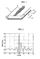
- FIG. 1 is a perspective view showing the schematic configuration of the reflection-type bandpass filter of the present invention.
- reference numeral 1 represents the reflection-type bandpass filter
- 2 the substrate
- 3 the conducting layer
- 4 the dielectric layer
- 5 the microstrip line.
- the z axis is taken along the lengthwise direction of the microstrip line 5, the y-axis perpendicular to the z-axis and along a direction parallel to the surface of the substrate 2, and the x-axis perpendicular to both the y-axis and the z-axis. From the end face on the input side, the length along the z-axis direction is taken as z.
- the reflection-type bandpass filter 1 has a substrate 2 laminated by a conducting layer 3 and dielectric layer 4, and a microstrip line 5 constituted by conductor having non-uniform width and provided on the dielectric layer 4.
- the distribution in the lengthwise direction of width of the microstrip line 5 is set such that : (1) the absolute value of the difference in reflectivity at the frequency f in the region f ⁇ 3.1 GHz and f>10.6 GHz and the reflectivity in the region 3.7 GHz ⁇ f ⁇ 10.0 GHz becomes equal or greater than 10 dB, the variation of the group delay in the region 3.7GHz ⁇ f ⁇ 10.0 GHz becomes within ⁇ 0.2 ns; or (2) the absolute value of the difference in reflectivity at the frequency f in the region f ⁇ 3.1 GHz and f>10.6 GHz and the reflectivity in the region 4.0 GHz ⁇ f ⁇ 9.8 GHz becomes equal or greater than 10 dB, the variation of the group delay in the region 4.0 GHz ⁇ f ⁇ 9.8 GHz becomes within ⁇ 0.1 ns; or (3) the absolute value of the difference in reflectivity at the frequency f in the region f ⁇ 3.1 GHz and f>10.6 GHz and the reflectivity in the
- the distribution in the lengthwise direction of width of the microstrip line 5 is set such that (1) the absolute value of the difference in reflectivity at the frequency f in the region f ⁇ 3.1 GHz and f>10.6 GHz and the reflectivity in the region 3.4 GHz ⁇ f ⁇ 10.3 GHz becomes equal or greater than 10 dB, the variation of the group delay in the region 3.4 GHz ⁇ f ⁇ 10.3 GHz becomes within ⁇ 0.2 ns; or (2) the absolute value of the difference in reflectivity at the frequency f in the region f ⁇ 3.1 GHz and f>10.6 GHz and the reflectivity in the region 3.6 GHz ⁇ f ⁇ 10.1 GHz becomes equal or greater than 10 dB, the variation of the group delay in the region 3.6 GHz ⁇ f ⁇ 10.1 GHz becomes within ⁇ 0.2 ns; or (3) the absolute value of the difference in reflectivity at the frequency f in the region f ⁇ 3.1 GHz and f>10.6 GHz and the reflectivity in the
- the reflection-type bandpass filter of the present invention was configured with increased stop band rejection by using the window function method (see Document 10) used in the design of digital filters.
- the stop band rejection can be increased. Therefore, manufacturing tolerances can be increased. The variation in the group delay frequency within the pass band will become small.
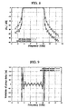
- the transmission line of the reflection-type bandpass filter 1 of the present invention can be expressed as a non-uniformly distributed parameter circuit, as shown in FIG. 5.
- L(z) and C(z) are the inductance and capacitance per unit length respectively in the transmission line.
- the function of equation (2) is introduced.
- ⁇ ⁇ ⁇ 1 z ⁇ t ⁇ z - 1 c z ⁇ ⁇ ⁇ 1 z ⁇ t ⁇ t - 1 2 ⁇ d ⁇ ln ⁇ Z z dz ⁇ ⁇ 2 z ⁇ t
- ⁇ ⁇ 2 z ⁇ t z 1 c z ⁇ ⁇ ⁇ 2 z ⁇ t t - 1 2 ⁇ d ⁇ ln ⁇ Z z dz ⁇ ⁇ 1 z ⁇ t .
- ⁇ 1 , ⁇ 2 are the power wave amplitudes propagating in the +z and -z directions respectively.
- c(z) 1/ ⁇ L(z)/C(z) ⁇ .
- the time factor is taken as exp(j ⁇ t)
- the Zakharov-Shabat equation as shown in the equation (5) can be obtained.
- Zakharov-Shabat The inverse problem of Zakharov-Shabat is the synthesis of the potential q(x) from the spectral data of the solution satisfying the equation above (see Document 11). If the potential q(x) is determined, then the local characteristic impedance can be found from equation (7) below.
- Z x Z 0 ⁇ exp 2 ⁇ ⁇ 0 x ⁇ q s ⁇ ds .
- the reflection coefficient r(x) of x space is calculated from the spectra data reflection coefficient R( ⁇ ) using the following equation (8), and q(x) is obtained from r(x).
- r x 1 2 ⁇ ⁇ ⁇ ⁇ - ⁇ ⁇ ⁇ R ⁇ ⁇ e - j ⁇ x d ⁇
- w(x) is a window function. If the window function is correctly selected, the level of the stop band rejection can be appropriately controlled.
- ⁇ M/2, and ⁇ is decided from experience as in equation (11) below.
- ⁇ ⁇ 0.1102 ⁇ A - 8.7 , A > 50 , 0.5842 ( A - 21 ⁇ ) 0.4 + 0.07886 ⁇ A - 21 , 21 ⁇ A ⁇ 50 , 0 , A ⁇ 21
- q(x) is determined, and the local characteristic impedance Z(x) is determined from equation (7).
- the local characteristic impedance and the width w of the microstrip line 5 are related to each other.
- the width w of the microstrip line 5 can be calculated from the value of the local characteristic impedance.
- the system characteristic impedance was taken as 50 Q, and the design was carried out.
- the characteristic impedance should be set such that it coincides with the impedance of the system being used.
- the system impedance 50 ⁇ , 75 ⁇ , 300 ⁇ , or similar is used.
- the characteristic impedance Zc should preferably be in the following range: 10 ⁇ ⁇ Zc ⁇ 300 ⁇ . If the characteristic impedance is less than 10 ⁇ , the loss due to conductor or dielectric will become relatively high. If the characteristic impedance is greater than 300 ⁇ , matching with the system impedance is not possible.
- Tables 1 through 3 list the widths w of the microstrip line 5 when the Kaiser window was used.
- FIG. 7 shows the shape of the microstrip line 5 in the reflection-type bandpass filter 1 of the embodiment 1.
- the non-reflecting terminator or resistance may be connected in series with the terminating end of the reflection-type bandpass filter 1.
- ⁇ , ⁇ 0 , and ⁇ each represent the angular frequency, the magnetic permeability in vacuum, and the conductivity of the metal.
- the thickness of the conducting layer 3 and of the conductor of the microstrip line 5 should be taken as 2.1 ⁇ m or greater.
- This reflection-type bandpass filter is used in a system where the characteristic impedance is 50 ⁇ .
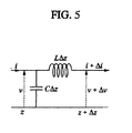
- FIG. 8 and FIG. 9 express the amplitude characteristics and group delay frequency characteristics respectively of the reflective wave (S11) in the bandpass filter of the embodiment 1.
- the characteristics when Kaiser window is not used are also shown.
- the reflectivity is -1 dB or greater and the variation of the group delay is within ⁇ 0.05 ns.
- the reflectivity is -17 dB or lower.
- the region of transition frequency becomes wider, but the stop band rejection increases to 15 dB, and the variation of group delay within the pass band decreases.
- Tables 4 through 6 list the widths w of the microstrip line 5 when the Kaiser window was used.
- FIG. 11 shows the shape of the microstrip line 5 in the reflection-type bandpass filter 1 of the embodiment 2.
- the thickness of the conducting layer 3 and of the conductor of the microstrip line 5 should be taken as 2.1 ⁇ m or greater.
- This reflection-type bandpass filter is used in a system where the characteristic impedance is 50 ⁇ .
- FIG. 12 and FIG. 13 express the amplitude characteristics and group delay frequency characteristics respectively of the reflective wave (S11) in the bandpass filter of the embodiment 2.
- the characteristics when Kaiser window is not used are also shown.
- the reflectivity is -2 dB or greater and the variation of the group delay is within ⁇ 0.03 ns.
- the reflectivity is -20 dB or lower.
- the region of transition frequency becomes wider, but the stop band rejection increases to 18 dB, and the variation of group delay within the pass band decreases.
- Tables 7 through 9 list the widths w of the microstrip line 5 when the Kaiser window was used.
- FIG. 15 shows the shape of the microstrip line 5 in the reflection-type bandpass filter 1 of the embodiment 3.
- the thickness of the conducting layer 3 and of the conductor of the microstrip line 5 should be taken as 2.1 ⁇ m or greater.
- This reflection-type bandpass filter is used in a system where the characteristic impedance is 30 ⁇ .
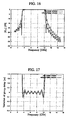
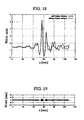
- FIG. 16 and FIG. 17 express the amplitude characteristics and group delay frequency characteristics respectively of the reflective wave (S11) in the bandpass filter of the embodiment 3.
- the characteristics when Kaiser window is not used are also shown, As shown in the figures, in the region of frequency f for which 3.5 GHz ⁇ f ⁇ 10.1 GHz, the reflectivity is -1 dB or greater and the variation of the group delay is within ⁇ 0.1 ns. In the region f ⁇ 3.1 GHz and f > 10.6 GHz, the reflectivity is -15 dB or lower.
- the region of transition frequency becomes wider, but the stop band rejection increases to 13 dB, and the variation of group delay within the pass band decreases.
- Tables 10 through 12 list the widths w of the microstrip line 5 when the Kaiser window was used.
- FIG. 19 shows the shape of the microstrip line 5 in the reflection-type bandpass fitter 1 of the embodiment 4.
- the thickness of the conducting layer 3 and of the conductor of the microstrip line 5 should be taken as 2.1 ⁇ m or greater.
- This reflectiort-type bandpass filter is used in a system where the characteristic impedance is 30 ⁇ .
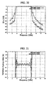
- FIG. 20 and FIG. 21 express the amplitude characteristics and group delay frequency characteristics respectively of the reflective wave (S11) in the bandpass filter of the embodiment 4.
- the characteristics when Kaiser window is not used are also shown.
- the reflectivity is -2 dB or greater and the variation of the group delay is within ⁇ 0.1 ns.
- the reflectivity is -20 dB or lower.
- the region of transition frequency becomes wider, but the stop band rejection increases to 18 dB, and the variation of group delay within the pass band decreases.
- Tables 13 through 15 list the widths w of the microstrip line 5 when the Kaiser window was used.
- FIG. 23 shows the shape of the microstrip line 5 in the reflection-type bandpass filter 1 of the embodiment 5.
- the thickness of the conducting layer 3 and of the conductor of the microstrip line 5 should be taken as 2,1 ⁇ m or greater.
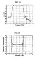
- This reflection-type bandpass filter is used in a system where the characteristic impedance is 50 ⁇ .
- FIG. 24 and FIG. 25 express the amplitude characteristics and group delay frequency characteristics respectively of the reflective wave (S11) in the bandpass filter of the embodiment 5. For comparison, the characteristics when Kaiser window is not used, are also shown. As shown in the figures, in the region of frequency f for which 4.0 GHz ⁇ f ⁇ 9.6 GHz, the reflectivity is -1 dB or greater and the variation of the group delay is within ⁇ 0.05 ns.
- FIG. 27 shows the shape of the microstrip line 5 in the reflection-type bandpass filter 1 of the embodiment 6.
- the thickness of the conducting layer 3 and of the conductor of the microstrip line 5 should be taken as 2.1 ⁇ m or greater.
- This reflection-type bandpass filter is used in a system where the characteristic impedance is 50 ⁇ .
- FIG. 28 and FIG. 29 express the amplitude characteristics and group delay frequency characteristics respectively of the reflective wave (S11) in the bandpass fitter of the embodiment 6.
- the reflectivity is -2 dB or greater and the variation of the group delay is within ⁇ 0.15 ns.
- the reflectivity is -15 dB or lower.
- Tables 17 through 19 list the widths w of the microstrip line 5.
- FIG. 31 shows the shape of the microstrip line 5 in the reflection-type bandpass filter 1 of the embodiment 7.
- the thickness of the conducting layer 3 and of the conductor of the microstrip line 5 should be taken as 2.1 ⁇ m or greater.
- This reflection-type bandpass filter is used in a system where the characteristic impedance is 50 ⁇ .
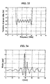
- FIG. 32 and FIG. 33 express the amplitude characteristics and group delay frequency characteristics respectively of the reflective wave (S11) in the bandpass filter of the embodiment 7.
- the reflectivity is -0.5 dB or greater and the variation of the group delay is within ⁇ 0.1 ns.
- the reflectivity is -10 dB or lower.
- Tables 20 through 22 list the widths w of the microstrip line 5.
- FIG. 35 shows the shape of the microstrip line 5 in the reflection-type bandpass filter 1 of the embodiment 8.
- the thickness of the conducting layer 3 and of the conductor of the microstrip line 5 should be taken as 2.1 ⁇ m or greater.
- This reflection-type bandpass filter is used in a system where the characteristic impedance is 30 ⁇ .
- FIG. 36 and FIG. 37 express the amplitude characteristics and group delay frequency characteristics respectively of the reflective wave (S11) in the bandpass filter of the embodiment 8, As shown in the figures, in the region of frequency f for which 3.4 GHz ⁇ f ⁇ 10.3 GHz, the reflectivity is -0.5 dB or greater and the variation of the group delay is within ⁇ 0.1 ns. In the region f ⁇ 3.1 GHz and f > 10.6 GHz, the reflectivity is -10 dB or lower.
- Tables 23 through 25 list the widths w of the microstrip line 5.
- FIG. 39 shows the shape of the microstrip line 5 in the reflection-type bandpass filter 1 of the embodiment 9.
- the thickness of the conducting layer 3 and of the conductor of the microstrip line 5 should be taken as 2.1 ⁇ m or greater.
- This reflection-type bandpass filter is used in a system where the characteristic impedance is 50 ⁇ .
- FIG. 40 and FIG. 41 express the amplitude characteristics and group delay frequency characteristics respectively of the reflective wave (S11) in the bandpass filter of the embodiment 9.
- the reflectivity is -1 dB or greater and the variation of the group delay is within ⁇ 0.1 ns.
- the reflectivity is -15 dB or lower.
- Table 26 lists the widths w of the microstrip line 5.
- FIG. 43 shows the shape of the microstrip line 5 in the reflection-type bandpass filter 1 of the embodiment 10.
- the thickness of the conducting layer 3 and of the conductor of the microstrip line 5 should be taken as 2.1 ⁇ m or greater.
- This reflection-type bandpass filter is used in a system where the characteristic impedance is 50 ⁇ .
- FIG. 44 and FIG. 45 express the amplitude characteristics and group delay frequency characteristics respectively of the reflective wave (S11) in the bandpass filter of the embodiment 10.
- the reflectivity is -2 dB or greater and the variation of the group delay is within ⁇ 0.15 ns.
- the reflectivity is -13 dB or lower.
Applications Claiming Priority (2)
| Application Number | Priority Date | Filing Date | Title |
|---|---|---|---|
| JP2006274322A JP2008098700A (ja) | 2006-10-05 | 2006-10-05 | 反射型バンドパスフィルター |
| JP2006321596A JP2008136062A (ja) | 2006-11-29 | 2006-11-29 | 反射型バンドパスフィルター |
Publications (1)
| Publication Number | Publication Date |
|---|---|
| EP1909354A1 true EP1909354A1 (de) | 2008-04-09 |
Family
ID=38777939
Family Applications (1)
| Application Number | Title | Priority Date | Filing Date |
|---|---|---|---|
| EP07117809A Withdrawn EP1909354A1 (de) | 2006-10-05 | 2007-10-03 | Reflektionsbandpassfilter |
Country Status (2)
| Country | Link |
|---|---|
| US (1) | US7855621B2 (de) |
| EP (1) | EP1909354A1 (de) |
Families Citing this family (3)
| Publication number | Priority date | Publication date | Assignee | Title |
|---|---|---|---|---|
| JP6730904B2 (ja) * | 2016-10-13 | 2020-07-29 | 株式会社フジクラ | 多重化装置 |
| US11431069B2 (en) | 2019-02-28 | 2022-08-30 | KYOCERA AVX Components Corporation | High frequency, surface mountable microstrip band pass filter |
| KR20200144846A (ko) | 2019-06-19 | 2020-12-30 | 삼성전자주식회사 | 외부 장치의 위치 정보를 결정하기 위한 전자 장치 및 그의 동작 방법 |
Citations (1)
| Publication number | Priority date | Publication date | Assignee | Title |
|---|---|---|---|---|
| SU1728904A1 (ru) * | 1990-03-14 | 1992-04-23 | Киевское высшее военное авиационное инженерное училище | Микрополосковый режекторный фильтр |
Family Cites Families (27)
| Publication number | Priority date | Publication date | Assignee | Title |
|---|---|---|---|---|
| GB579414A (en) | 1941-10-15 | 1946-08-02 | Standard Telephones Cables Ltd | Improvements in or relating to electric wave filters |
| US3617877A (en) * | 1969-07-01 | 1971-11-02 | Us Navy | Coaxial line measurement device having metal strip filter |
| US4371853A (en) | 1979-10-30 | 1983-02-01 | Matsushita Electric Industrial Company, Limited | Strip-line resonator and a band pass filter having the same |
| JPS5664501A (en) | 1979-10-30 | 1981-06-01 | Matsushita Electric Ind Co Ltd | Strip line resonator |
| CH663690A5 (en) | 1983-09-22 | 1987-12-31 | Feller Ag | Line having a distributed low-pass filter |
| US4992760A (en) | 1987-11-27 | 1991-02-12 | Hitachi Metals, Ltd. | Magnetostatic wave device and chip therefor |
| US5418507A (en) * | 1991-10-24 | 1995-05-23 | Litton Systems, Inc. | Yig tuned high performance filters using full loop, nonreciprocal coupling |
| US5525953A (en) | 1993-04-28 | 1996-06-11 | Murata Manufacturing Co., Ltd. | Multi-plate type high frequency parallel strip-line cable comprising circuit device part integratedly formed in dielectric body of the cable |
| JP3350792B2 (ja) | 1993-04-28 | 2002-11-25 | 株式会社村田製作所 | 平行ストリップラインケーブル |
| JPH09172318A (ja) | 1995-12-19 | 1997-06-30 | Hisamatsu Nakano | 円偏波マイクロストリップラインアンテナ |
| US5923295A (en) | 1995-12-19 | 1999-07-13 | Mitsumi Electric Co., Ltd. | Circular polarization microstrip line antenna power supply and receiver loading the microstrip line antenna |
| JPH09232820A (ja) | 1996-02-27 | 1997-09-05 | Toshiba Corp | マイクロストリップ線路 |
| JPH1065402A (ja) | 1996-06-26 | 1998-03-06 | Korea Electron Telecommun | マイクロストリップオープンスタブ線路方式の低域通過フィルターおよびその製造方法 |
| JP3001825B2 (ja) | 1997-02-28 | 2000-01-24 | 社団法人関西電子工業振興センター | マイクロストリップラインアンテナ |
| JP3527410B2 (ja) | 1998-06-15 | 2004-05-17 | 株式会社リコー | コプレーナーストリップライン |
| JP3289694B2 (ja) | 1998-07-24 | 2002-06-10 | 株式会社村田製作所 | 高周波回路装置および通信装置 |
| JP3587354B2 (ja) | 1999-03-08 | 2004-11-10 | 株式会社村田製作所 | 横結合共振子型表面波フィルタ及び縦結合共振子型表面波フィルタ |
| JP3650957B2 (ja) * | 1999-07-13 | 2005-05-25 | 株式会社村田製作所 | 伝送線路、フィルタ、デュプレクサおよび通信装置 |
| JP2001339203A (ja) | 2000-05-29 | 2001-12-07 | Murata Mfg Co Ltd | デュアルモード・バンドパスフィルタ |
| JP2002043810A (ja) | 2000-07-21 | 2002-02-08 | Sony Corp | マイクロストリップ線路 |
| US6603376B1 (en) | 2000-12-28 | 2003-08-05 | Nortel Networks Limited | Suspended stripline structures to reduce skin effect and dielectric loss to provide low loss transmission of signals with high data rates or high frequencies |
| US20040145954A1 (en) | 2001-09-27 | 2004-07-29 | Toncich Stanley S. | Electrically tunable bandpass filters |
| US6924714B2 (en) * | 2003-05-14 | 2005-08-02 | Anokiwave, Inc. | High power termination for radio frequency (RF) circuits |
| KR100576773B1 (ko) * | 2003-12-24 | 2006-05-08 | 한국전자통신연구원 | 종단 결합된 sir들을 이용한 마이크로스트립대역통과필터 |
| KR20060113539A (ko) | 2005-04-28 | 2006-11-02 | 쿄세라 코포레이션 | 대역통과 필터 및 이것을 사용한 무선통신기기 |
| KR100806389B1 (ko) | 2006-01-09 | 2008-02-27 | 삼성전자주식회사 | Paralle coupled cpw line 필터 |
| US8081707B2 (en) | 2006-03-13 | 2011-12-20 | Xg Technology, Inc. | Carrier less modulator using saw filters |
-
2007
- 2007-10-03 EP EP07117809A patent/EP1909354A1/de not_active Withdrawn
- 2007-10-04 US US11/867,440 patent/US7855621B2/en not_active Expired - Fee Related
Patent Citations (1)
| Publication number | Priority date | Publication date | Assignee | Title |
|---|---|---|---|---|
| SU1728904A1 (ru) * | 1990-03-14 | 1992-04-23 | Киевское высшее военное авиационное инженерное училище | Микрополосковый режекторный фильтр |
Non-Patent Citations (4)
| Title |
|---|
| DA-CHIANG CHANG ET AL: "Wide-Band Equal-Ripple Filters inNonuniform Transmission Lines", IEEE TRANSACTIONS ON MICROWAVE THEORY AND TECHNIQUES, IEEE SERVICE CENTER, PISCATAWAY, NJ, US, vol. 50, no. 4, April 2002 (2002-04-01), XP011076539, ISSN: 0018-9480 * |
| GAOBIAO XIAO ET AL: "A New Numerical Method for Synthesis of Arbitrarily Terminated Lossless NonuniformTransmission Lines", IEEE TRANSACTIONS ON MICROWAVE THEORY AND TECHNIQUES, IEEE SERVICE CENTER, PISCATAWAY, NJ, US, vol. 49, no. 2, February 2001 (2001-02-01), XP011038268, ISSN: 0018-9480 * |
| GAOBIAO XIAO ET AL: "Impedance Matching for Complex Loads Through Nonuniform Transmission Lines", IEEE TRANSACTIONS ON MICROWAVE THEORY AND TECHNIQUES, IEEE SERVICE CENTER, PISCATAWAY, NJ, US, vol. 50, no. 6, June 2002 (2002-06-01), XP011076613, ISSN: 0018-9480 * |
| RENATO DE PÁDUA MOREIRA ET AL: "Direct Synthesis of Microwave Filters Using Inverse Scattering Transmission-Line Matrix Method", IEEE TRANSACTIONS ON MICROWAVE THEORY AND TECHNIQUES, IEEE SERVICE CENTER, PISCATAWAY, NJ, US, vol. 48, no. 12, December 2000 (2000-12-01), XP011038181, ISSN: 0018-9480 * |
Also Published As
| Publication number | Publication date |
|---|---|
| US7855621B2 (en) | 2010-12-21 |
| US20080106355A1 (en) | 2008-05-08 |
Similar Documents
| Publication | Publication Date | Title |
|---|---|---|
| US20100188167A1 (en) | Ku-band diplexer | |
| Boutejdar et al. | Design and improvement of a compact bandpass filter using DGS technique for WLAN and WiMAX applications | |
| EP1909354A1 (de) | Reflektionsbandpassfilter | |
| JP2008098700A (ja) | 反射型バンドパスフィルター | |
| EP1909352A1 (de) | Reflektionsbandpassfilter | |
| US7839240B2 (en) | Reflection-type banpass filter | |
| Das et al. | Compact High-Selectivity Wide Stopband Microstrip Cross-Coupled Bandpass Filter With Spurline | |
| Jung et al. | A highly selective UWB bandpass filter using stepped impedance stubs | |
| Al-Naib et al. | Single metal layer CPW metamaterial bandpass filter | |
| EP1909351B1 (de) | Reflektionsbandpassfilter | |
| EP1912277A1 (de) | Reflektionsbandpassfilter | |
| Karthie et al. | Fractal-based triangular bandpass filter with a notched band for interference rejection in wideband applications | |
| Marimuthu et al. | Wideband and harmonic suppression method of parallel coupled microstrip bandpass filter using centered single groove | |
| Al-Areqi et al. | Design of microstrip parallel-coupled line band pass filters for the application in fifth generation wireless communication | |
| Rautschke et al. | Comparison of conventional and substrate integrated waveguide filters for satellite communication | |
| Tabei et al. | A compact wideband bandstop filter using microstrip ring structure | |
| Jovanović | Extended Configuration of Antiparallel Band Pass Filters with Two Independently Adjustable Transmission Zeros. | |
| Cui et al. | A triple-layer frequency selective surface with flat wide passband | |
| Almalkawi et al. | Compact realization of combline bandpass filter integrated with defected microstrip structure bandstop filter | |
| Farhat et al. | Microstrip bandpass filter with wide stopband and high out-of-band rejection | |
| Uchida et al. | An elliptic-function bandpass filter utilizing left-handed operations of an inter-digital coupled line | |
| Firmli et al. | Design of Ultra-Wideband (UWB) Bandpass Filters Based on Interdigital Edge Coupled Lines: A Review | |
| T Hammed | Miniaturized Dual-Band Bandstop Filter Using Multilayered E-Shape Microstrip Structure | |
| JP2009272753A (ja) | 透過型導波路バンドパスフィルタ及びその設計方法 | |
| Singh et al. | A Compact 3 rd Order SIW Filter with Improved Upper Band Performance for Ku-Band Applications |
Legal Events
| Date | Code | Title | Description |
|---|---|---|---|
| PUAI | Public reference made under article 153(3) epc to a published international application that has entered the european phase |
Free format text: ORIGINAL CODE: 0009012 |
|
| 17P | Request for examination filed |
Effective date: 20071003 |
|
| AK | Designated contracting states |
Kind code of ref document: A1 Designated state(s): AT BE BG CH CY CZ DE DK EE ES FI FR GB GR HU IE IS IT LI LT LU LV MC MT NL PL PT RO SE SI SK TR |
|
| AX | Request for extension of the european patent |
Extension state: AL BA HR MK RS |
|
| AKX | Designation fees paid |
Designated state(s): DE FR GB IT |
|
| STAA | Information on the status of an ep patent application or granted ep patent |
Free format text: STATUS: THE APPLICATION IS DEEMED TO BE WITHDRAWN |
|
| 18D | Application deemed to be withdrawn |
Effective date: 20081010 |