EP1908273B1 - Pixel binning and averaging based on illumination - Google Patents
Pixel binning and averaging based on illumination Download PDFInfo
- Publication number
- EP1908273B1 EP1908273B1 EP06787654.0A EP06787654A EP1908273B1 EP 1908273 B1 EP1908273 B1 EP 1908273B1 EP 06787654 A EP06787654 A EP 06787654A EP 1908273 B1 EP1908273 B1 EP 1908273B1
- Authority
- EP
- European Patent Office
- Prior art keywords
- color
- pixel values
- pixel
- consecutive
- subset
- Prior art date
- Legal status (The legal status is an assumption and is not a legal conclusion. Google has not performed a legal analysis and makes no representation as to the accuracy of the status listed.)
- Active
Links
Images


Classifications
-
- H—ELECTRICITY
- H04—ELECTRIC COMMUNICATION TECHNIQUE
- H04N—PICTORIAL COMMUNICATION, e.g. TELEVISION
- H04N23/00—Cameras or camera modules comprising electronic image sensors; Control thereof
- H04N23/80—Camera processing pipelines; Components thereof
- H04N23/84—Camera processing pipelines; Components thereof for processing colour signals
- H04N23/88—Camera processing pipelines; Components thereof for processing colour signals for colour balance, e.g. white-balance circuits or colour temperature control
-
- H—ELECTRICITY
- H04—ELECTRIC COMMUNICATION TECHNIQUE
- H04N—PICTORIAL COMMUNICATION, e.g. TELEVISION
- H04N25/00—Circuitry of solid-state image sensors [SSIS]; Control thereof
- H04N25/10—Circuitry of solid-state image sensors [SSIS]; Control thereof for transforming different wavelengths into image signals
- H04N25/11—Arrangement of colour filter arrays [CFA]; Filter mosaics
- H04N25/13—Arrangement of colour filter arrays [CFA]; Filter mosaics characterised by the spectral characteristics of the filter elements
- H04N25/134—Arrangement of colour filter arrays [CFA]; Filter mosaics characterised by the spectral characteristics of the filter elements based on three different wavelength filter elements
-
- H—ELECTRICITY
- H04—ELECTRIC COMMUNICATION TECHNIQUE
- H04N—PICTORIAL COMMUNICATION, e.g. TELEVISION
- H04N25/00—Circuitry of solid-state image sensors [SSIS]; Control thereof
- H04N25/40—Extracting pixel data from image sensors by controlling scanning circuits, e.g. by modifying the number of pixels sampled or to be sampled
- H04N25/44—Extracting pixel data from image sensors by controlling scanning circuits, e.g. by modifying the number of pixels sampled or to be sampled by partially reading an SSIS array
- H04N25/445—Extracting pixel data from image sensors by controlling scanning circuits, e.g. by modifying the number of pixels sampled or to be sampled by partially reading an SSIS array by skipping some contiguous pixels within the read portion of the array
-
- H—ELECTRICITY
- H04—ELECTRIC COMMUNICATION TECHNIQUE
- H04N—PICTORIAL COMMUNICATION, e.g. TELEVISION
- H04N25/00—Circuitry of solid-state image sensors [SSIS]; Control thereof
- H04N25/40—Extracting pixel data from image sensors by controlling scanning circuits, e.g. by modifying the number of pixels sampled or to be sampled
- H04N25/44—Extracting pixel data from image sensors by controlling scanning circuits, e.g. by modifying the number of pixels sampled or to be sampled by partially reading an SSIS array
- H04N25/447—Extracting pixel data from image sensors by controlling scanning circuits, e.g. by modifying the number of pixels sampled or to be sampled by partially reading an SSIS array by preserving the colour pattern with or without loss of information
-
- H—ELECTRICITY
- H04—ELECTRIC COMMUNICATION TECHNIQUE
- H04N—PICTORIAL COMMUNICATION, e.g. TELEVISION
- H04N25/00—Circuitry of solid-state image sensors [SSIS]; Control thereof
- H04N25/40—Extracting pixel data from image sensors by controlling scanning circuits, e.g. by modifying the number of pixels sampled or to be sampled
- H04N25/46—Extracting pixel data from image sensors by controlling scanning circuits, e.g. by modifying the number of pixels sampled or to be sampled by combining or binning pixels
Definitions
- the invention relates generally to the field of subsampling of pixels of an image sensor. More specifically, the invention relates to subsampling pixels of an image sensor that changes pixel sensitivity to account for scene illuminant changes.
- Subsampling image sensors for reducing spatial resolution is performed for purposes such as increasing processing speed and the like.
- Fig. 1 there is shown a Bayer color filter array (CFA) used for creating color images on the image sensor.
- CFA Bayer color filter array
- prior art image sensors are subsampled by skipping pixels (designated by the X) as shown in Fig. 2 .
- the prior art reduces resolution by combining pixels as shown in Fig. 3 .
- the individual colors are combined both vertically and horizontally as shown by the curved lines.
- the resulting subsampled image for both Fig. 2 and Fig. 3 have sampling characteristics that are not optimal for representing the subsampled image.
- the pixels that comprise the subsampled image are not evenly spaced but are instead grouped together. This results in a perceived lower resolution image than might be anticipated by the amount of subsampling done.
- US 2004/0125223A1 patent application discloses a method for driving a solid-state image pickup apparatus, a solid-state image pickup device and a camera which enables fast operation and makes applicable of the conventional algorithm in signal processings by reducing the number of samples in the horizontal and vertical directions.
- Three or more odd number pixels in the solid-state image pickup device are made one block, signal charges of predetermined pixels being thinned out to be transferred to transfer registers, resulting signal charges being added within the transfer registers so that the center of gravity of pixels (pixel center) may coincide with a pixel at the center of one block and resulting mixed charge being transferred.
- Three transfer electrodes are provided per one column of the vertical register in a part of the vertical register on the side of the horizontal register.
- the vertical registers arranged in a three column cycle constitute the solid-state image pickup device.
- the camera is constructed to have a switching mode of operation between a mode in which mixed charges that result from adding signal charges in predetermined pixels of one block are output, and a normal mode of taking a picture.
- a solid-state image pick-up apparatus wherein a solid-state image sensor includes a color filter having filter segments arranged in a pattern, photosensitive cells for photoelectrically transducing light transmitted through the filter segments to generate corresponding signal charges, vertical transfer devices for vertically transferring the signal charges, a horizontal transfer device for transferring the signal charges input from the vertical transfer devices in the horizontal direction, and a charge holding circuit intervening between the vertical and horizontal transfer devices for temporarily storing the signal charges.
- a signal charge thinning circuit omits signal charges whose color pattern, which is generated by mixing signal charges having the same color attribute in the direction of row in the filter pattern to thereby horizontally thin the signal charges, is different in positional relation from the filter pattern.
- the present invention is directed to overcoming one or more of the problems set forth above. According to one aspect of the present invention, the present invention is directed to a method as set out in claim 1 and a method as set out in claim 3.
- the present invention has the following advantage of permitting selective combining and subsampling of colors based on lighting conditions in order to improve the inherent white balance, or chromatic sensitivity, of the image sensor, while also improving the spatial sampling pattern of the resulting reduced resolution image. It also includes the advantage of permitting extended dynamic range in the reduced resolution image when certain combining and subsampling approaches are used.
- the invention will be described in the context of a commonly known Bayer color filter array pattern. It is to be understood that the present invention is applicable to both types of image sensors, CCDs (charge-coupled devices) and active pixel (also commonly known as CMOS) image sensors. It is also noted that a two-dimensional array can be retrieved from any image whether on a sensor or in electronic memory.
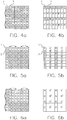
- the patent application will first describe subsampling in the y direction that also improves the sensitivity of the subsampled blue pixels ( Figs. 4a and 4b ), then will describe subsampling in the x direction with similar improvement in blue sensitivity ( Figs. 5a and 5b ), and then will describe an embodiment of the invention where there is subsampling in both y and x directions with still further improvement in blue sensitivity ( Figs. 6a and 6b ).
- a top view of an example two dimensional image sensor which is not an embodiment of the present invention, but is useful for understanding the invention.
- the sensor is covered and spanned by a color filter array, typically a Bayer color filter, for creating pixels containing different colors.
- the present example is directed to subsampling the image sensor to create a smaller resolution image that exhibits a different color balance than that of a non-subsampled image or prior art subsampled images.
- the non-subsampled image may be better suited for capturing images in daylight and the subsampled image may be better suited for capturing images in incandescent light.
- the image sensor of the present example periodically combines at least two pixel values of a same first color, the color blue in column 2, in the y direction of the two dimensional array. It is further noted that green is combined in column 1.
- the combined pixel values of the first color are read out of the sensor, via a horizontal shift register in a CCD image sensor and by addressable column circuits in a CMOS image sensor.
- the non-combined pixels are also read out in the y direction of the two dimensional array.
- the non-combined colors are red in column 1 and green in column 2.
- the second color is periodically skipped or not read out.
- the second color is red in column 1 and green in column 2. This is accomplished by not addressing these pixels in a CMOS image sensor and by a fast dump gate in a CCD image sensor.
- the periodicity is formed by skipping the color between the combined colors.
- the skipped colors are indicated by Xs in Fig. 4a .
- subsampling by the above described method produces an image having combined first colors and second colors that are uniform in spacing.
- the image may alternatively be subsampled in the x direction by repeating the above described process with column 1 being analogous to row 1 and column 2 analogous to row 2.
- the subsampling in the x and y directions may be done separately or, in embodiments of the present invention, combined as in Figs. 6a and 6b for producing the desired subsampled image.
- Figs. 6a and 6b which provide an embodiment of the invention, have the further advantage of additional improvement in blue sensitivity, because additional blue pixels from the original image are combined.
- Figs. 7a and 7b there is shown an alternative decimation arrangement analogous to Figs. 4a and 4b but with improved sensitivity to red light instead of blue light.
- the image sensor of Figs. 7a and 7b which is not an embodiment of the present invention but is useful for understanding the invention, periodically combines at least two pixel values of a same first color, the red in column 1, in the y direction of the two dimensional array. It is further noted that green is combined in column 2.
- the combined pixel values of the first color are read out to the sensor.
- the non-combined pixels are also read out in the y direction of the two dimensional array.
- the non-combined colors are blue in column 2 and green in column 1.
- the second color is periodically skipped or not read out.
- the second color is blue in column 2 and green in column 1.
- the periodicity is formed by skipping the color between the combined colors.
- the skipped colors are indicated by Xs in Fig. 7a .
- Figs. 8a and 8b correspond to Figs. 5a and 5b
- Figs. 9a and 9b which correspond to Figs. 6a and 6b
- Improved sensitivity to blue light may be suited to capturing images illuminated by incandescent light
- improved sensitivity to red light may be suited to capturing images illuminated by fluorescent light.
- Choosing one subsampling scheme over another may be performed automatically by sensor circuitry or by algorithmic examination of the sensor scene data. The selectivity may be performed manually by simply permitting the user to override the automatic function and select the appropriate light based on the sensed lighting conditions.
- Figs. 4b, 5b , 7b, and 8b it is seen that in addition to the combined blue or red color there are also both a non-combined green result and a combined green result. These two green results effectively provide two different green sensitivities in the resulting image.
- the two green sensitivities can be used to extend the dynamic range of the captured image, with the non-combined green pixels being effective at capturing and reproducing bright areas of the image, the combined green pixels being effective at capturing and reproducing dark areas of the image, and areas of the image that are between the light and dark areas may be effectively represented by both the non-combined and the combined green pixels.
- Figs. 4b, 5b , 7b, and 8b it is seen that in addition to the combined blue or red color there are also both a non-combined green result and a combined green result.
- 10a and 10b which provides another embodiment of the invention, selectively combining and not combining green pixels in both the horizontal and vertical directions (analogous to combining blue pixels and not combining red pixels in Figs. 6a and 6b or to combining red pixels and not combining blue pixels in Figs. 9a and 9b ) provides a further increase in dynamic range based on the green pixels while not affecting the speed of the red and blue combined pixels relative to each other.
Landscapes
- Engineering & Computer Science (AREA)
- Multimedia (AREA)
- Signal Processing (AREA)
- Physics & Mathematics (AREA)
- Spectroscopy & Molecular Physics (AREA)
- Color Television Image Signal Generators (AREA)
- Image Processing (AREA)
- Transforming Light Signals Into Electric Signals (AREA)
- Facsimile Image Signal Circuits (AREA)
- Color Image Communication Systems (AREA)
Applications Claiming Priority (2)
| Application Number | Priority Date | Filing Date | Title |
|---|---|---|---|
| US11/185,393 US8306362B2 (en) | 2005-07-20 | 2005-07-20 | Selective pixel binning and averaging based on scene illuminant |
| PCT/US2006/027776 WO2007015835A1 (en) | 2005-07-20 | 2006-07-18 | Pixel binning and averaging based on illumination |
Publications (2)
| Publication Number | Publication Date |
|---|---|
| EP1908273A1 EP1908273A1 (en) | 2008-04-09 |
| EP1908273B1 true EP1908273B1 (en) | 2018-05-09 |
Family
ID=37389844
Family Applications (1)
| Application Number | Title | Priority Date | Filing Date |
|---|---|---|---|
| EP06787654.0A Active EP1908273B1 (en) | 2005-07-20 | 2006-07-18 | Pixel binning and averaging based on illumination |
Country Status (7)
| Country | Link |
|---|---|
| US (1) | US8306362B2 (enExample) |
| EP (1) | EP1908273B1 (enExample) |
| JP (2) | JP5114400B2 (enExample) |
| KR (1) | KR101246410B1 (enExample) |
| CN (1) | CN101223772B (enExample) |
| TW (1) | TWI394445B (enExample) |
| WO (1) | WO2007015835A1 (enExample) |
Families Citing this family (27)
| Publication number | Priority date | Publication date | Assignee | Title |
|---|---|---|---|---|
| US8274715B2 (en) | 2005-07-28 | 2012-09-25 | Omnivision Technologies, Inc. | Processing color and panchromatic pixels |
| US8139130B2 (en) | 2005-07-28 | 2012-03-20 | Omnivision Technologies, Inc. | Image sensor with improved light sensitivity |
| US7916362B2 (en) * | 2006-05-22 | 2011-03-29 | Eastman Kodak Company | Image sensor with improved light sensitivity |
| US8031258B2 (en) | 2006-10-04 | 2011-10-04 | Omnivision Technologies, Inc. | Providing multiple video signals from single sensor |
| US7999870B2 (en) * | 2008-02-01 | 2011-08-16 | Omnivision Technologies, Inc. | Sampling and readout of an image sensor having a sparse color filter array pattern |
| US7781716B2 (en) * | 2008-03-17 | 2010-08-24 | Eastman Kodak Company | Stacked image sensor with shared diffusion regions in respective dropped pixel positions of a pixel array |
| US20100309340A1 (en) * | 2009-06-03 | 2010-12-09 | Border John N | Image sensor having global and rolling shutter processes for respective sets of pixels of a pixel array |
| US8546737B2 (en) * | 2009-10-30 | 2013-10-01 | Invisage Technologies, Inc. | Systems and methods for color binning |
| JP5775570B2 (ja) * | 2010-06-01 | 2015-09-09 | 博立▲碼▼杰通▲訊▼(深▲せん▼)有限公司Boly Media Communications(Shenzhen)Co.,Ltd. | マルチスペクトル感光素子及びそのサンプリング方法 |
| JP5640509B2 (ja) * | 2010-07-09 | 2014-12-17 | ソニー株式会社 | 固体撮像素子およびカメラシステム |
| US8780238B2 (en) | 2011-01-28 | 2014-07-15 | Aptina Imaging Corporation | Systems and methods for binning pixels |
| GB2488769A (en) * | 2011-03-07 | 2012-09-12 | Sony Corp | Image Sensor Including an Array of Primary Colour Sensitive Photosensors Being Read in Line Subsets |
| JP5833961B2 (ja) * | 2012-03-23 | 2015-12-16 | 株式会社東芝 | 画像圧縮装置、画像処理システム、及び画像圧縮方法 |
| US9407837B2 (en) | 2013-02-28 | 2016-08-02 | Google Inc. | Depth sensor using modulated light projector and image sensor with color and IR sensing |
| US9398287B2 (en) | 2013-02-28 | 2016-07-19 | Google Technology Holdings LLC | Context-based depth sensor control |
| KR102178335B1 (ko) | 2014-01-02 | 2020-11-12 | 삼성전자주식회사 | 이미지 센서의 비닝 방법 및 이미지 센서 |
| JP2015156556A (ja) * | 2014-02-20 | 2015-08-27 | 株式会社東芝 | 固体撮像装置 |
| CN103872065B (zh) * | 2014-03-10 | 2016-09-21 | 北京空间机电研究所 | 垂直电荷转移成像探测器像元合并方法 |
| US9978801B2 (en) | 2014-07-25 | 2018-05-22 | Invisage Technologies, Inc. | Multi-spectral photodetector with light-sensing regions having different heights and no color filter layer |
| CN104241309B (zh) * | 2014-09-19 | 2018-01-02 | 上海集成电路研发中心有限公司 | 一种模拟随机像素效果的cmos图像像素阵列 |
| CN104819991A (zh) * | 2015-05-15 | 2015-08-05 | 北京华力兴科技发展有限责任公司 | 可变分辨率的辐射成像方法、系统和装置 |
| US9986189B2 (en) | 2016-01-04 | 2018-05-29 | Samsung Electronics Co., Ltd. | Pixel sensors and imaging devices for providing multiple sub sample images within a single frame |
| US10277840B2 (en) | 2016-01-11 | 2019-04-30 | Semiconductor Components Industries, Llc | Methods for clocking an image sensor |
| US11025842B2 (en) | 2019-04-05 | 2021-06-01 | Apple Inc. | Binner circuit for image signal processor |
| CN113711584B (zh) * | 2020-03-20 | 2023-03-03 | 华为技术有限公司 | 一种摄像装置 |
| KR20210148682A (ko) | 2020-06-01 | 2021-12-08 | 삼성전자주식회사 | 이미지 센서, 이미지 센서를 포함하는 모바일 장치 및 이미지 센서의 센싱 감도 제어 방법 |
| KR20230152464A (ko) | 2022-04-27 | 2023-11-03 | 삼성전자주식회사 | 이미지 센서의 비닝 방법 및 이를 수행하는 이미지 센서 |
Citations (2)
| Publication number | Priority date | Publication date | Assignee | Title |
|---|---|---|---|---|
| JP2000032345A (ja) * | 1998-07-10 | 2000-01-28 | Olympus Optical Co Ltd | 撮像装置 |
| US20030169355A1 (en) * | 2002-03-07 | 2003-09-11 | Naoki Kubo | Solid-state image pickup apparatus with horizontal thinning and a signal reading method for the same |
Family Cites Families (18)
| Publication number | Priority date | Publication date | Assignee | Title |
|---|---|---|---|---|
| US4591900A (en) | 1983-03-14 | 1986-05-27 | Rca Corporation | Encoding pattern for single chip CCD camera processing scheme |
| JP4329128B2 (ja) * | 1996-07-12 | 2009-09-09 | ソニー株式会社 | 固体撮像装置、固体撮像装置の駆動方法およびカメラ |
| US6057586A (en) | 1997-09-26 | 2000-05-02 | Intel Corporation | Method and apparatus for employing a light shield to modulate pixel color responsivity |
| US5990950A (en) | 1998-02-11 | 1999-11-23 | Iterated Systems, Inc. | Method and system for color filter array multifactor interpolation |
| JP4140077B2 (ja) | 1998-02-18 | 2008-08-27 | ソニー株式会社 | 固体撮像素子の駆動方法及び固体撮像素子、並びにカメラ |
| TW391129B (en) | 1998-04-30 | 2000-05-21 | Hyundai Electronics Ind | Apparatus and method for compressing image data outputted from image semsor having bayer pattern |
| JPH11331706A (ja) | 1998-05-15 | 1999-11-30 | Sony Corp | 固体撮像素子およびその駆動方法、並びにカメラシステム |
| JP4361991B2 (ja) * | 1999-08-20 | 2009-11-11 | メディア・テック・ユーエスエイ・インコーポレーテッド | 画像処理装置 |
| US6784930B1 (en) * | 1999-11-29 | 2004-08-31 | Agilent Technologies, Inc. | Active pixel sensor with enhanced reset |
| JP2002185871A (ja) | 2000-12-12 | 2002-06-28 | Sony Corp | 固体撮像素子及びその駆動方法 |
| US7292274B2 (en) * | 2001-11-06 | 2007-11-06 | Eastman Kodak Company | Solid-state image pickup device driving method and image capturing apparatus for outputting high-resolution signals for still images and moving images of improved quality at a high frame rate |
| JP3968122B2 (ja) * | 2001-12-13 | 2007-08-29 | イーストマン コダック カンパニー | 撮像装置 |
| US6970608B1 (en) * | 2001-12-30 | 2005-11-29 | Cognex Technology And Investment Corporation | Method for obtaining high-resolution performance from a single-chip color image sensor |
| JP2004112738A (ja) * | 2002-07-25 | 2004-04-08 | Fujitsu Ltd | 単板式カラーイメージセンサの解像度変換方法及び画素データ処理回路 |
| DE10245715A1 (de) * | 2002-10-01 | 2004-04-15 | Philips Intellectual Property & Standards Gmbh | Verfahren und Vorrichtung zur Erzeugung von Teilabbildungen |
| JP4458236B2 (ja) * | 2003-09-30 | 2010-04-28 | パナソニック株式会社 | 固体撮像装置 |
| JP4624065B2 (ja) * | 2004-10-13 | 2011-02-02 | オリンパス株式会社 | 撮像装置 |
| US7538807B2 (en) * | 2004-11-23 | 2009-05-26 | Dalsa Corporation | Method and apparatus for in a multi-pixel pick-up element reducing a pixel-based resolution and/or effecting anti-aliasing through selectively combining selective primary pixel outputs to combined secondary pixel outputs |
-
2005
- 2005-07-20 US US11/185,393 patent/US8306362B2/en active Active
-
2006
- 2006-06-23 TW TW095122752A patent/TWI394445B/zh active
- 2006-07-18 CN CN200680026084XA patent/CN101223772B/zh active Active
- 2006-07-18 JP JP2008522882A patent/JP5114400B2/ja active Active
- 2006-07-18 KR KR1020087001467A patent/KR101246410B1/ko active Active
- 2006-07-18 EP EP06787654.0A patent/EP1908273B1/en active Active
- 2006-07-18 WO PCT/US2006/027776 patent/WO2007015835A1/en not_active Ceased
-
2012
- 2012-07-06 JP JP2012152843A patent/JP5619825B2/ja active Active
Patent Citations (2)
| Publication number | Priority date | Publication date | Assignee | Title |
|---|---|---|---|---|
| JP2000032345A (ja) * | 1998-07-10 | 2000-01-28 | Olympus Optical Co Ltd | 撮像装置 |
| US20030169355A1 (en) * | 2002-03-07 | 2003-09-11 | Naoki Kubo | Solid-state image pickup apparatus with horizontal thinning and a signal reading method for the same |
Also Published As
| Publication number | Publication date |
|---|---|
| US20070030366A1 (en) | 2007-02-08 |
| KR20080030028A (ko) | 2008-04-03 |
| JP5114400B2 (ja) | 2013-01-09 |
| CN101223772A (zh) | 2008-07-16 |
| JP5619825B2 (ja) | 2014-11-05 |
| EP1908273A1 (en) | 2008-04-09 |
| KR101246410B1 (ko) | 2013-03-21 |
| TWI394445B (zh) | 2013-04-21 |
| US8306362B2 (en) | 2012-11-06 |
| TW200729929A (en) | 2007-08-01 |
| WO2007015835A1 (en) | 2007-02-08 |
| CN101223772B (zh) | 2012-12-12 |
| JP2009503939A (ja) | 2009-01-29 |
| JP2012231521A (ja) | 2012-11-22 |
Similar Documents
| Publication | Publication Date | Title |
|---|---|---|
| EP1908273B1 (en) | Pixel binning and averaging based on illumination | |
| US6992714B1 (en) | Image pickup apparatus having plural pixels arranged two-dimensionally, and selective addition of different pixel color signals to control spatial color arrangement | |
| US8310573B2 (en) | Solid-state imaging device, signal processing method thereof and image capturing apparatus | |
| CN1086534C (zh) | 图象传感设备 | |
| US7440019B2 (en) | Solid-state image pick-up device | |
| CN103392336B (zh) | 固态成像设备和相机系统 | |
| EP2194721A2 (en) | solid-state imaging device, method for processing signal of solid-state imaging device, and imaging apparatus | |
| US8111298B2 (en) | Imaging circuit and image pickup device | |
| JP2003218343A (ja) | 固体撮像装置 | |
| KR100462260B1 (ko) | 영상픽업장치 | |
| EP1349399A2 (en) | Solid state color image pickup device | |
| EP0800317B1 (en) | Single CCD-type color camera having high resolution and capable of restricting generation of ghost color | |
| US20050117039A1 (en) | Solid-state imaging device | |
| US20040017493A1 (en) | Resolution conversion method and pixel data processing circuit for single-plate-type color-image sensor | |
| US7701498B2 (en) | Solid-state image pickup device, drive method therefor and camera | |
| JP2004023683A (ja) | 固体撮像素子の欠陥補正装置及び方法 | |
| US7932942B2 (en) | Solid-state imaging device including three stacked photoelectric conversion layers, three accumulators, and a single readout circuit | |
| US20060197859A1 (en) | Solid-state image sensor having its photosensitive cells broadened in area | |
| Singh et al. | Double Binnable RGB, RGBW and LMS Color Filter Arrays | |
| WO2002085035A1 (fr) | Dispositif d'imagerie a semiconducteur | |
| JPH0946716A (ja) | 固体撮像装置の駆動方法 | |
| JPH0414983A (ja) | 固体撮像装置及びその駆動方法 | |
| JPH0965075A (ja) | リニアセンサとその出力の信号処理装置 | |
| JP2004146955A (ja) | 固体撮像素子及びその駆動方法 | |
| JPH0564069A (ja) | 撮像装置 |
Legal Events
| Date | Code | Title | Description |
|---|---|---|---|
| PUAI | Public reference made under article 153(3) epc to a published international application that has entered the european phase |
Free format text: ORIGINAL CODE: 0009012 |
|
| 17P | Request for examination filed |
Effective date: 20071221 |
|
| AK | Designated contracting states |
Kind code of ref document: A1 Designated state(s): DE FR GB NL |
|
| RBV | Designated contracting states (corrected) |
Designated state(s): DE FR GB NL |
|
| 17Q | First examination report despatched |
Effective date: 20090114 |
|
| RAP1 | Party data changed (applicant data changed or rights of an application transferred) |
Owner name: OMNIVISION TECHNOLOGIES, INC. |
|
| DAX | Request for extension of the european patent (deleted) | ||
| REG | Reference to a national code |
Ref country code: DE Ref legal event code: R079 Ref document number: 602006055368 Country of ref document: DE Free format text: PREVIOUS MAIN CLASS: H04N0003150000 Ipc: H04N0005345000 |
|
| GRAP | Despatch of communication of intention to grant a patent |
Free format text: ORIGINAL CODE: EPIDOSNIGR1 |
|
| INTG | Intention to grant announced |
Effective date: 20180108 |
|
| RIC1 | Information provided on ipc code assigned before grant |
Ipc: H04N 5/345 20110101AFI20171218BHEP Ipc: H04N 9/04 20060101ALI20171218BHEP Ipc: H04N 5/347 20110101ALI20171218BHEP |
|
| GRAS | Grant fee paid |
Free format text: ORIGINAL CODE: EPIDOSNIGR3 |
|
| GRAA | (expected) grant |
Free format text: ORIGINAL CODE: 0009210 |
|
| AK | Designated contracting states |
Kind code of ref document: B1 Designated state(s): DE FR GB NL |
|
| REG | Reference to a national code |
Ref country code: GB Ref legal event code: FG4D |
|
| REG | Reference to a national code |
Ref country code: DE Ref legal event code: R096 Ref document number: 602006055368 Country of ref document: DE |
|
| REG | Reference to a national code |
Ref country code: FR Ref legal event code: PLFP Year of fee payment: 13 |
|
| REG | Reference to a national code |
Ref country code: NL Ref legal event code: FP |
|
| REG | Reference to a national code |
Ref country code: DE Ref legal event code: R097 Ref document number: 602006055368 Country of ref document: DE |
|
| PLBE | No opposition filed within time limit |
Free format text: ORIGINAL CODE: 0009261 |
|
| STAA | Information on the status of an ep patent application or granted ep patent |
Free format text: STATUS: NO OPPOSITION FILED WITHIN TIME LIMIT |
|
| 26N | No opposition filed |
Effective date: 20190212 |
|
| REG | Reference to a national code |
Ref country code: DE Ref legal event code: R079 Ref document number: 602006055368 Country of ref document: DE Free format text: PREVIOUS MAIN CLASS: H04N0005345000 Ipc: H04N0025440000 |
|
| PGFP | Annual fee paid to national office [announced via postgrant information from national office to epo] |
Ref country code: GB Payment date: 20250612 Year of fee payment: 20 |
|
| PGFP | Annual fee paid to national office [announced via postgrant information from national office to epo] |
Ref country code: NL Payment date: 20250618 Year of fee payment: 20 |
|
| PGFP | Annual fee paid to national office [announced via postgrant information from national office to epo] |
Ref country code: FR Payment date: 20250612 Year of fee payment: 20 |
|
| PGFP | Annual fee paid to national office [announced via postgrant information from national office to epo] |
Ref country code: DE Payment date: 20250616 Year of fee payment: 20 |