EP1905602A2 - Linsenmatrix, Belichtungsvorrichtung, Bilderzeugungsvorrichtung und Lesevorrichtung - Google Patents
Linsenmatrix, Belichtungsvorrichtung, Bilderzeugungsvorrichtung und Lesevorrichtung Download PDFInfo
- Publication number
- EP1905602A2 EP1905602A2 EP07117136A EP07117136A EP1905602A2 EP 1905602 A2 EP1905602 A2 EP 1905602A2 EP 07117136 A EP07117136 A EP 07117136A EP 07117136 A EP07117136 A EP 07117136A EP 1905602 A2 EP1905602 A2 EP 1905602A2
- Authority
- EP
- European Patent Office
- Prior art keywords
- lens
- lens array
- lenses
- light
- array according
- Prior art date
- Legal status (The legal status is an assumption and is not a legal conclusion. Google has not performed a legal analysis and makes no representation as to the accuracy of the status listed.)
- Ceased
Links
- 230000003287 optical effect Effects 0.000 claims abstract description 116
- 239000000463 material Substances 0.000 claims description 15
- 239000011347 resin Substances 0.000 claims description 13
- 229920005989 resin Polymers 0.000 claims description 13
- 150000001875 compounds Chemical class 0.000 claims description 11
- 238000000465 moulding Methods 0.000 claims description 9
- 230000000052 comparative effect Effects 0.000 description 83
- 238000012546 transfer Methods 0.000 description 20
- 230000015556 catabolic process Effects 0.000 description 14
- 238000006731 degradation reaction Methods 0.000 description 14
- 230000004075 alteration Effects 0.000 description 10
- 230000008901 benefit Effects 0.000 description 10
- 238000009826 distribution Methods 0.000 description 9
- 230000001965 increasing effect Effects 0.000 description 9
- 230000007423 decrease Effects 0.000 description 7
- 238000005259 measurement Methods 0.000 description 6
- 230000009467 reduction Effects 0.000 description 6
- 238000002474 experimental method Methods 0.000 description 5
- 238000012795 verification Methods 0.000 description 5
- 230000000903 blocking effect Effects 0.000 description 4
- 239000003086 colorant Substances 0.000 description 4
- 238000005520 cutting process Methods 0.000 description 4
- 238000011156 evaluation Methods 0.000 description 4
- 238000000034 method Methods 0.000 description 4
- 102220616555 S-phase kinase-associated protein 2_E48R_mutation Human genes 0.000 description 3
- 150000001925 cycloalkenes Chemical class 0.000 description 3
- 230000001747 exhibiting effect Effects 0.000 description 3
- 239000011159 matrix material Substances 0.000 description 3
- 239000013307 optical fiber Substances 0.000 description 3
- 239000012780 transparent material Substances 0.000 description 3
- 238000003491 array Methods 0.000 description 2
- 230000001276 controlling effect Effects 0.000 description 2
- 229910052736 halogen Inorganic materials 0.000 description 2
- 150000002367 halogens Chemical class 0.000 description 2
- 239000004973 liquid crystal related substance Substances 0.000 description 2
- 238000012986 modification Methods 0.000 description 2
- 230000004048 modification Effects 0.000 description 2
- 239000004065 semiconductor Substances 0.000 description 2
- 229910001220 stainless steel Inorganic materials 0.000 description 2
- 239000010935 stainless steel Substances 0.000 description 2
- 239000000758 substrate Substances 0.000 description 2
- VYZAMTAEIAYCRO-UHFFFAOYSA-N Chromium Chemical compound [Cr] VYZAMTAEIAYCRO-UHFFFAOYSA-N 0.000 description 1
- 239000011247 coating layer Substances 0.000 description 1
- 230000000694 effects Effects 0.000 description 1
- 230000002708 enhancing effect Effects 0.000 description 1
- 238000005530 etching Methods 0.000 description 1
- 239000003365 glass fiber Substances 0.000 description 1
- 238000005304 joining Methods 0.000 description 1
- 239000010410 layer Substances 0.000 description 1
- 238000004020 luminiscence type Methods 0.000 description 1
- 238000004519 manufacturing process Methods 0.000 description 1
- 238000005192 partition Methods 0.000 description 1
- 230000002093 peripheral effect Effects 0.000 description 1
- 239000000049 pigment Substances 0.000 description 1
- 239000004417 polycarbonate Substances 0.000 description 1
- 229920000515 polycarbonate Polymers 0.000 description 1
- 230000001105 regulatory effect Effects 0.000 description 1
Images


Classifications
-
- B—PERFORMING OPERATIONS; TRANSPORTING
- B41—PRINTING; LINING MACHINES; TYPEWRITERS; STAMPS
- B41J—TYPEWRITERS; SELECTIVE PRINTING MECHANISMS, i.e. MECHANISMS PRINTING OTHERWISE THAN FROM A FORME; CORRECTION OF TYPOGRAPHICAL ERRORS
- B41J2/00—Typewriters or selective printing mechanisms characterised by the printing or marking process for which they are designed
- B41J2/435—Typewriters or selective printing mechanisms characterised by the printing or marking process for which they are designed characterised by selective application of radiation to a printing material or impression-transfer material
- B41J2/447—Typewriters or selective printing mechanisms characterised by the printing or marking process for which they are designed characterised by selective application of radiation to a printing material or impression-transfer material using arrays of radiation sources
- B41J2/45—Typewriters or selective printing mechanisms characterised by the printing or marking process for which they are designed characterised by selective application of radiation to a printing material or impression-transfer material using arrays of radiation sources using light-emitting diode [LED] or laser arrays
- B41J2/451—Special optical means therefor, e.g. lenses, mirrors, focusing means
-
- G—PHYSICS
- G02—OPTICS
- G02B—OPTICAL ELEMENTS, SYSTEMS OR APPARATUS
- G02B27/00—Optical systems or apparatus not provided for by any of the groups G02B1/00 - G02B26/00, G02B30/00
- G02B27/0018—Optical systems or apparatus not provided for by any of the groups G02B1/00 - G02B26/00, G02B30/00 with means for preventing ghost images
-
- G—PHYSICS
- G02—OPTICS
- G02B—OPTICAL ELEMENTS, SYSTEMS OR APPARATUS
- G02B3/00—Simple or compound lenses
- G02B3/0006—Arrays
- G02B3/0037—Arrays characterized by the distribution or form of lenses
- G02B3/005—Arrays characterized by the distribution or form of lenses arranged along a single direction only, e.g. lenticular sheets
-
- G—PHYSICS
- G02—OPTICS
- G02B—OPTICAL ELEMENTS, SYSTEMS OR APPARATUS
- G02B3/00—Simple or compound lenses
- G02B3/0006—Arrays
- G02B3/0037—Arrays characterized by the distribution or form of lenses
- G02B3/0056—Arrays characterized by the distribution or form of lenses arranged along two different directions in a plane, e.g. honeycomb arrangement of lenses
-
- G—PHYSICS
- G02—OPTICS
- G02B—OPTICAL ELEMENTS, SYSTEMS OR APPARATUS
- G02B3/00—Simple or compound lenses
- G02B3/0006—Arrays
- G02B3/0037—Arrays characterized by the distribution or form of lenses
- G02B3/0062—Stacked lens arrays, i.e. refractive surfaces arranged in at least two planes, without structurally separate optical elements in-between
- G02B3/0068—Stacked lens arrays, i.e. refractive surfaces arranged in at least two planes, without structurally separate optical elements in-between arranged in a single integral body or plate, e.g. laminates or hybrid structures with other optical elements
-
- G—PHYSICS
- G02—OPTICS
- G02B—OPTICAL ELEMENTS, SYSTEMS OR APPARATUS
- G02B5/00—Optical elements other than lenses
- G02B5/003—Light absorbing elements
-
- G—PHYSICS
- G03—PHOTOGRAPHY; CINEMATOGRAPHY; ANALOGOUS TECHNIQUES USING WAVES OTHER THAN OPTICAL WAVES; ELECTROGRAPHY; HOLOGRAPHY
- G03G—ELECTROGRAPHY; ELECTROPHOTOGRAPHY; MAGNETOGRAPHY
- G03G15/00—Apparatus for electrographic processes using a charge pattern
- G03G15/04—Apparatus for electrographic processes using a charge pattern for exposing, i.e. imagewise exposure by optically projecting the original image on a photoconductive recording material
- G03G15/0409—Details of projection optics
-
- G—PHYSICS
- G03—PHOTOGRAPHY; CINEMATOGRAPHY; ANALOGOUS TECHNIQUES USING WAVES OTHER THAN OPTICAL WAVES; ELECTROGRAPHY; HOLOGRAPHY
- G03G—ELECTROGRAPHY; ELECTROPHOTOGRAPHY; MAGNETOGRAPHY
- G03G2215/00—Apparatus for electrophotographic processes
- G03G2215/01—Apparatus for electrophotographic processes for producing multicoloured copies
- G03G2215/0103—Plural electrographic recording members
- G03G2215/0119—Linear arrangement adjacent plural transfer points
- G03G2215/0138—Linear arrangement adjacent plural transfer points primary transfer to a recording medium carried by a transport belt
- G03G2215/0141—Linear arrangement adjacent plural transfer points primary transfer to a recording medium carried by a transport belt the linear arrangement being horizontal
-
- G—PHYSICS
- G03—PHOTOGRAPHY; CINEMATOGRAPHY; ANALOGOUS TECHNIQUES USING WAVES OTHER THAN OPTICAL WAVES; ELECTROGRAPHY; HOLOGRAPHY
- G03G—ELECTROGRAPHY; ELECTROPHOTOGRAPHY; MAGNETOGRAPHY
- G03G2215/00—Apparatus for electrophotographic processes
- G03G2215/04—Arrangements for exposing and producing an image
- G03G2215/0429—Changing or enhancing the image
- G03G2215/0431—Producing a clean non-image area, i.e. avoiding show-around effects
- G03G2215/0448—Charge-erasing means for the non-image area
- G03G2215/0451—Light-emitting array or panel
- G03G2215/0453—Light-emitting diodes, i.e. LED-array
Definitions
- This invention relates to a lens array, an exposure device, an image forming apparatus and a reading apparatus.
- an image forming apparatus such as a printer, a copier, a compound machine or the like
- an image forming apparatus uses an array of rod lenses disposed in opposition to the light emitting portions.
- the rod lenses are configured to focus the lights emitted by the light emitting portions onto a surface of a photosensitive drum.
- a reading device such as a scanner having an array of light receiving portions.
- Such a reading device uses an array of rod lenses disposed in opposition to the light receiving portions.
- the rod lens is an optical element formed of a glass fiber impregnated with ion so that the refractive index decreases from the center portion toward the peripheral portion.
- the rod lens forms an erected image at the same magnification.
- a lens array in which rod lenses are arranged in a plurality of rows is used as an optical system for focusing an image of an object as a linear image.
- a lens array in which rod lenses are arranged in a single row. Further, there is proposed another lens array including lens-pairs each of which includes a pair of micro lenses disposed at an interval corresponding to the focal length so that optical axes thereof are aligned with each other (see, for example, Japanese Laid-Open Patent Publication No. 2002-107661 ).
- the lens array using the micro lenses has the same function as the lens array using the rod lenses.
- An object of the present invention is to solve the above described problems, and an object of the present invention is to provide a lens array, an exposure device, an image forming apparatus and a reading apparatus capable of enhancing the resolution and increasing the amount of light.
- the present invention provides a lens array including a plurality of lens groups each of which includes lenses so disposed that optical axes thereof are aligned with each other.
- the lens groups are arranged in a direction perpendicular to the optical axes.
- a light-blocking portion is provided for shielding each of the lens groups from light having passed through any lens of other lens groups.
- a largest diameter D of each lens, and an arrangement interval P at which the lens groups are arranged satisfy the relationship: P ⁇ D.
- the largest diameter D of the lens is larger than the arrangement interval P of the lens groups, it becomes possible to prevent the degradation of the resolution and the reduction of the amount of light (that otherwise occur with a cycle corresponding to the arrangement interval of the lenses).
- the present invention also provides a lens array including a plurality of lenses.
- the plurality of lenses include first and second lenses arranged in a first direction at an arrangement interval P Y , and third and fourth lenses arranged in a second direction at an arrangement interval P N .
- the arrangement intervals P Y and P N satisfy the relationship: P Y > P N .
- the arrangement interval P N in the second direction is smaller than the arrangement interval P Y between the lenses in the first direction, the resolution can be enhanced, and the amount of light can be increased.
- the printer uses a toner, i.e., a developer, composed of a resin containing a pigment (as a coloring agent), and is configured to form an image such as a color image or a monochrome image on a sheet as a medium in accordance with image data.
- a toner i.e., a developer
- a resin containing a pigment as a coloring agent
- FIG. 1 is a schematic view showing a printer according to the first embodiment of the present invention.
- a printer 10 includes a main body (i.e., an apparatus main body) in which a substantially S-shaped feeding path 25 is provided for feeding a not shown sheet (i.e., a medium). Feeding rollers 26, 27, 28 and 29 are disposed along the feeding path 25. Further, image forming units Bk, Y, M and C are disposed along the feeding path 25, for forming the toner images (developer images) of the respective colors. A transfer unit 34 is disposed below the image forming units Bk, Y, M and C, for feeding the sheet and for transferring the respective toner images to the sheet. The feeding path 25 is formed between the respective image forming units Bk, Y, M and C and the transfer unit 34. The transfer unit 34 constitutes a belt driving unit.
- LED heads 23 i.e., exposure devices or recording heads
- LED heads 23 are disposed in the printer 10 in such a manner that the LED heads 23 face respective photosensitive drums (i.e., image bearing bodies) 11 of the image forming units Bk, Y, M and C.
- a fixing unit 35 is disposed on the downstream side of the transfer unit 34, for fixing the toner image (having been transferred to the sheet) to the sheet.
- the photosensitive drum 11 has an electrically chargeable surface, and rotates at a predetermined speed.
- the surface of the photosensitive drum 11 is exposed with light emitted by the LED head 23, and the electric charge of the exposed surface of the photosensitive drum 11 is removed, so that the latent image is formed thereon.
- a charging roller 12 i.e., a charging device
- the charging roller 12 rotates in the direction opposite to the rotational direction of the photosensitive drum 11 and applies a predetermined voltage to the surface of the photosensitive drum 11.
- a developing device 45 is disposed in opposition to the photosensitive drum 11, and develops the latent image to form a toner image.
- the developing device 45 includes a developing roller 16 (i.e., a developer bearing body) causing the toner to adhere to the photosensitive drum 11, a not shown developing blade regulating the thickness of the toner layer formed on the surface of the developing roller 16, a toner supply roller 18 (i.e., a developer supply roller) supplying the toner to the developing roller 16, and the like.
- the developing roller 16 is urged against the photosensitive drum 11 at a constant pressure, and rotates in the direction opposite to the rotational direction of the photosensitive drum 11.
- the toner supply roller 18 is urged against the developing roller 16 at a constant pressure, and rotates in the same direction as the rotational direction of the developing roller 16.
- the photosensitive drum 11, the charging roller 12, the developing device 45 and the like are housed in a casing 20 that constitutes a main body of the image forming unit.
- a toner cartridge 15 (as a developer storing portion) storing the toner is detachably attached to the casing 20.
- the transfer unit 34 includes a movable transfer belt 21, and transfer rollers 22 (i.e., transfer members) respectively disposed in opposition to the photosensitive drums 11.
- the transfer belt 21 and the transfer rollers 22 are applied with predetermined voltages by not shown power sources, and transfer the respective toner images from the photosensitive drums 11 to the sheet.
- the printer 10 includes a lower frame 38 and an upper frame 40 swingably provided on the lower frame 38.
- the upper frame 40 includes a stacker 31 for stacking the ejected sheets thereon.
- a sheet cassette 30 i.e., a media storing portion
- the sheet cassette 30 has a sheet pickup portion 32 that picks up and feeds the sheet out of the sheet cassette 30.
- the charging rollers 12 uniformly charge the surfaces of the photosensitive drums 11.
- the LED heads 23 expose the surfaces of the photosensitive drums 11, and form latent images thereon.
- the developing devices 45 develop the latent images and form toner images of the respective colors.
- the sheet is picked up by the sheet pickup portion 32, is fed by the feeding rollers 26 and 27, and adheres to the transfer belt 21 by means of an electrostatic effect.
- the transfer belt 21 By the movement of the transfer belt 21, the sheet is fed through between the image forming units Bk, Y, M and C and the transfer unit 34, and the toner images of the respective colors are transferred to the sheet in an overlapping manner, with the result that the color toner image is formed on the sheet.
- the sheet reaches the fixing unit 35, and the color toner image is fixed to the sheet.
- the sheet is further fed by the feeing rollers 28 and 29, and is ejected to the stacker 31.
- the printer 10 includes an external interface (not shown) for communicating with an external device and for receiving print data.
- the printer 10 further includes a control unit that receives the print data via the external interface and controls the whole of the printer.
- the LED head 23 will be described.
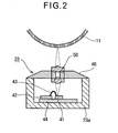
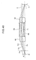
- FIG. 2 is a cross sectional view of the LED head 23 according to the first embodiment of the present invention.
- the LED head 23 includes a lens array 50.
- the lens array 50 is fixed to a supporting body 23a by means of a holding member 46.
- the LED head 23 includes light emitting portions 41 that emit light to the photosensitive drum 11.
- the light emitting portions 41 include a plurality of LED elements (i.e., light emitting elements) linearly arranged. In this embodiment, the number of the LED elements per inch (approximately 25.4 mm) is 600.
- a light-blocking member (not shown) is disposed between the light emitting portions 41 and the lens array 50.
- the light emitting portions 41 and a driver IC 42 for controlling the light emission of the LED elements of the light emitting portions 41 are provided on a wiring substrate 44 (disposed on the supporting body 23a).
- the light emitting portions 41 and the driver IC 42 are connected with each other by means of wires 43.
- the above described control unit generates control signal for the LED head 23 in accordance with the image data, and sends the control signal to the driver IC 42.
- the driver IC 42 causes the LED elements of the light emitting portions 41 to respectively emit lights of predetermined amounts according to the control signal. Then, the lights emitted by the respective LED elements are incident on the lens array 50, pass through the lens array 50, and are focused on the photosensitive drum 11, so that the focused images of the light emitting portions 41 are formed on the photosensitive drum 11.
- the lens array 50 will be described.
- FIG. 3A is a partially cutaway plan view showing the lens array 50 according to the first embodiment of the present invention.
- FIG. 3B is a schematic perspective view of a light-blocking portion of the lens array.
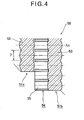
- FIGS. 4 and 5 are a longitudinal sectional view and a cross sectional view showing the lens array 50 according to the first embodiment of the present invention.
- the lens array 50 includes a pair of lens plates 51a and 51b that face with each other.
- the lens array 50 further includes a light-blocking portion 54 disposed between the lens plates 51a and 51b and made of material that blocks the light.
- the light-blocking portion 54 has a plurality of openings 55.
- a plurality of micro lenses 53 are integrally formed on each of the lens plates 51a and 51b, and are disposed at the center portions of the lens plates 51a and 51b in the width direction.
- the micro lenses 53 are arranged in the direction perpendicular to the optical axes of the micro lenses 53 (i.e., arranged in the longitudinal direction of the lens plates 51a and 51b).
- Each of the micro lenses 53 of the lens plate 51a and the corresponding one of the micro lenses 53 of the lens plate 51b have optical axes aligned with each other, and constitute a lens-pair (i.e., a lens group) 52.
- Each micro lens 53 constitutes an optical element that forms an inverted image at a reduced magnification.
- the lens pair 52 constitutes an optical element that forms an erected image at the same magnification.
- each micro lens 53 has a rotationally-symmetric shape with respect to the optical axis (indicated by the mark Ax in FIG. 3A).
- the curved surface of the micro lens 53 is so shaped that the curved surface of the micro lens 53 is cut by a plane parallel to the optical axis in the vicinity of the border with the adjacent micro lens 53.
- a largest diameter D of the micro lens 53 is defined as a diameter of a circle which circumscribes the micro lens 53 and whose center is aligned with the optical axis of the micro lens 53.
- the lens plates 51a and 51b and the light-blocking portion 54 are so disposed that the optical axes of the lens pairs 52 are aligned with the centers of the openings 55.
- an interval (center-to-center distance) at which the micro lenses 53 are arranged is referred to as an arrangement interval P.
- the arrangement interval P of the micro lenses 53 and the diameter D of each micro lens 53 are so set as to satisfy the relationship: P ⁇ D.
- the opening 55 of the light-blocking portion 54 has a dimension (i.e., an opening dimension in the width direction) W X in the direction perpendicular to the direction in which the micro lenses 53 are arranged, and a dimension (i.e., an opening dimension in the arranging direction) W Y in the direction parallel to the direction in which the micro lenses 53 are arranged.
- the dimensions W X and W Y satisfy the relationship: W Y ⁇ W X .
- the opening 55 has a substantially cylindrical shape whose diameter is the same as the opening dimension W X and whose center is aligned with the optical axis, and bounded by two planes parallel to the optical axis disposed at an interval which is the same as the opening dimension W Y .
- a lens array of a comparative example is prepared for the verification of the advantage of this embodiment.
- a lens array 50' (see FIGS. 9 and 10) of the comparative example is so configured that the arrangement interval P of the micro lenses 53' is the same as the diameter D of each micro lens 53', and the micro lens 53' has a circular shape as seen in the direction of the optical axis.
- the dimensions W Y and W X of the opening 55' of the light-blocking portion 54' are the same as each other.
- the opening 55' has a cylindrical shape whose diameter is the same as the opening dimension W Y and whose center is aligned with the optical axis.
- the lens plates 51a and 51b are formed of cycloolefin-based resin "ZEONEX E48R" (product name) manufactured by Nihon Zeon Corporation and formed by resin molding.
- the light-blocking portion 54 (54') is formed of polycarbonate and formed by resin molding.
- FIG. 6 is a schematic view showing an arrangement of optical elements according to the first embodiment of the present invention.
- the mark L 0 indicates the distance between the lens array 50 and the light emitting portion 41 (i.e., the distance between an object plane and a lens surface), and is defined by the distance between the apex of an outer curved surface 53a of the micro lens 53 and a plane (i.e., an object plane P1) on which the light emitting portions 41 are arranged.
- the mark L I indicates the distance (i.e., the distance between an image plane and a lens surface) between the lens array 50 and the photosensitive drum 11 on which an image I is focused, and is defined by the distance between the apex of an outer curved surface 53a of the micro lens 53 and a plane (i.e., an image plane P2) on which the photosensitive drum 11 is disposed.
- the mark L T indicates the lens thickness L T , and is defined by the distance between the outer curved surface 53a and the inner curved surface 53b of the micro lens 53.
- the mark L S indicates the distance between lens surfaces, and is defined by the distance between the respective inner curved surfaces 53b of the micro lenses 53 of the lens-pair 52.
- the mark TC indicates the distance between the image plane P2 and the object plane P1, and is defined by the distance between the photosensitive drum 11 and the light emitting portion 41.
- outer curved surface 53a and the inner curved surface 53b of the micro lens 53 are respectively rotationally-symmetric high-order aspheric surfaces, and expressed as the following equations (1) and (2):
- Z O r r 2 C o 1 + 1 - r C O 2 + A O ⁇ r 4 + B O ⁇ r 6
- Z I r r 2 C I 1 + 1 - r C I 2 + A I ⁇ r 4 + B I ⁇ r 6
- Each of the functions Z O (r) and Z I (r) indicates a rotating coordinate system whose axis is parallel to the optical axis of the micro lens 53 and in which the radial coordinate is expressed as "r".
- the apexes of the outer curved surface 53a and the inner curved surface 53b of the micro lens 53 are defined as original points.
- the direction from the object plane toward the image plane is expressed as being positive number.
- the mark C o indicates a radius of curvature of the outer curved surface 53a.
- the mark A o indicates a fourth-order aspherical coefficient of the outer curved surface 53a.
- the mark B o indicates a sixth-order aspherical coefficient of the outer curved surface 53a.
- the mark C I indicates a radius of curvature of the inner curved surface 53b.
- the mark A I indicates a fourth-order aspherical coefficient of the inner curved surface 53b.
- the mark B I indicates a sixth-order aspherical coefficient of the inner curved surface 53b.
- micro lenses 53 are integrally formed with the lens plates 51a and 51b, it is also possible to individually form the micro lenses 53 and to fix the micro lenses 53 to the lens plates 51a and 51b at predetermined intervals.
- the outer curved surface 53a and the inner curved surface 53b are rotationally-symmetric high-order aspheric surfaces in this embodiment, the outer curved surface 53a and the inner curved surface 53b can be spherical surfaces. Moreover, the outer curved surface 53a and the inner curved surface 53b can be conic surfaces (such as paraboloidal surfaces, ellipsoidal surfaces, hyperboloidal surfaces or the like), toroidal surfaces (asymmetric in respective directions perpendicular to the optical axis) and cylindrical surfaces or the like. Further, the outer curved surface 53a and the inner curved surface 53b can be conventional free curved surfaces.
- the micro lens 53 is formed of a transparent material (that transmits the light from the light source) having a uniform refractive index and having predetermined curved surfaces. However, it is also possible to use a lens, optical fibers or the like having a predetermined distribution of refractive index.
- the light-blocking portion 54 is formed by resin molding in this embodiment, the light-blocking portion 54 can be formed by cutting work. Further, it is also possible to form a light-blocking pattern of a light-blocking material (that blocks the light emitted by the light source) on a material that transmits the light. It is also possible to form a light-blocking pattern using a light-blocking material partially on the lens plates 51a and 51b. It is also possible to partially roughen the surfaces of the lens plates 51a and 51b to block the light. It is also possible to partially cut off the lens plates 51a and 51b to prevent the incidence of a part of the light.
- the LED elements i.e., the LED array
- organic EL (Electric Luminescence) elements are used as the light emitting portions 41.
- semiconductor lasers it is also possible to use a light source such as a fluorescent lamp, halogen lamp or the like together with a shutter composed of a liquid crystal display.
- FIGS. 7 and 8 are a plan view and a sectional view showing the lens array of the first embodiment of the present invention.
- FIGS. 9 and 10 are a plan view and a sectional view showing the lens array of the comparative example with respect to the first embodiment of the present invention.
- the lens array 50 of the first embodiment and the lens array 50' of the comparative example are configured as shown in TABLE 1.
- a reference numeral 41a indicates a light emitting portion (among the light emitting portions 41) disposed on a position corresponding to a border between adjacent micro lenses 53 (53').
- the lens array 50' of the comparative example is used to form the focused image I of the light emitting portion 41a, the resolution and the amount of light are smaller than those when the lens array 50 of the first embodiment of the present invention is used.
- FIGS. 8 and 10 show respective paths of the lights passing through the lens arrays 50 and 50' and reaching the photosensitive drum 11 to form the focused image I.
- a light ray traveling along the shortest path is defined as a principal ray R M .
- a light ray travelling along the outermost path from the principal ray R M is defined as a rim ray Rs.
- the light emitted by the light emitting portion 41a is incident on the micro lens 53 (53') on the light emitting portion 41a side of the lens pair 52 (52'), forms the focused image of the light emitting portion 41a at the reduced magnification, and is incident on the micro lens 53 (53') on the photosensitive drum 11 side.
- the micro lens 53 (53') of the photosensitive drum 11 side forms an inverted image of the image (having been focused at the reduced magnification) of the light emitting portion 41a at the enlarged magnification.
- the lens pair 52 (52') focuses an erected image of the light emitting portion 41a on the surface of the photosensitive drum 11 at the same magnification.
- the light emitting portion 41a is closer to the optical axis Ax of the micro lens 53, compared with the lens array 50' of the comparative example.
- the aberration becomes smaller and the amount of light increases, as the object is closer to the optical axis of the lens.
- the rim ray R S of the light emitted by the light emitting portion 41a has a larger angle ⁇ 0 , compared with the rim ray R S of the lens array 50' of the comparative example. Therefore, when the lens array 50 according to the first embodiment is used, the amount of the light incident on the micro lens 53 (of the total amount of the light emitted by the light emitted portion 41a) is larger than that when the lens array 50' of the comparative example is used. Accordingly, the focused image I of the light emitting portion 41a using the lens array 50 of the first embodiment is brighter than the focused image I of the light emitting portion 41a using the lens array 50' of the comparative example.
- the optical axes Ax of the micro lenses 53 of the lens array 50 of the first embodiment are closer to the light emitting portions 41a than the optical axes Ax of the micro lenses 53' of the lens array 50' of the comparative example.
- the aberration in the focused image I is smaller when the lens array 50 of the first embodiment is used than when the lens array 50' of the comparative example is used. Therefore, according to the first embodiment of the present invention, it becomes possible to form a sharp image and to obtain a bright image (with large amount of light). Further, it becomes possible to prevent the degradation of the resolution and the reduction of the amount of light (that otherwise occur with a cycle corresponding to the arrangement interval of the micro lenses 53 of the lens array 50).
- MTF Modulation Transfer Function, i.e., amplitude transfer function
- the MTF indicates a resolution of the focused image, i.e., a contrast in the amount of light forming the focused image by means of the activated LED elements of the LED head 23.
- a resolution of the focused image i.e., a contrast in the amount of light forming the focused image by means of the activated LED elements of the LED head 23.
- FIG. 11 is a graph showing the MTF of the lens array of the first embodiment of the present invention.
- FIG. 12 is a graph showing the MTF of the lens array of the comparative example.
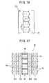
- FIG. 13 is a graph showing the distribution of the amount of light of the lens array of the first embodiment of the present invention.
- FIG. 14 is a graph showing the distribution of the amount of light of the lens array of the comparative example.
- the horizontal axis indicates the position on the image plane
- the vertical axis indicates the MTF.
- the horizontal axis indicates the position on the image plane
- the vertical axis indicates the amount of light.
- the lens array 50 of the first embodiment and the lens array 50' of the comparative example are respectively mounted on the LED head 23 of the color LED printer having the resolution of 600 dpi.
- a microscopic digital camera is used to take the focused image at a position distanced from the outer curved surface 53 on the image plane side (the photosensitive drum 11 side) by the distance L I (i.e., the distance L1 between the image plane and the lens surface).
- the distribution of the amount of light forming the focused image of the light emitting portion is analyzed, and the MTF and the amount of light are calculated.
- the MTF on each position is expressed as a proportion (percentage) to the maximum value of the MTF.
- the amount of light on each position is expressed as a proportion (percentage) to the maximum value of the amount of light.
- FIGS. 11 through 14 show the experimental results on the positions in the range of 20 mm.
- the range of fluctuation of the MTF is approximately 50 % as shown in FIG. 12.
- the range of fluctuation of the MTF is approximately 5 % as shown in FIG. 11.
- the range of fluctuation of the amount of light is approximately 40 % as shown in FIG. 14.
- the range of fluctuation of the amount of light is approximately 20 % as shown in FIG. 13.
- the LED head 23 of the first embodiment of the present invention is controlled by the driver IC 42 so that the LED elements emit constant amount of lights, the range of fluctuation can be reduced to less than or equal to 1 %.
- the LED head of the comparative example can not be controlled to cause the LED elements to emit constant amount of lights.
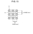
- the "1 ⁇ 1" image is an image in which dots D are alternately formed at 300 dpi (i.e., at the interval of 0.0423 mm ⁇ 2) in the vertical and horizontal directions on the dot matrix of 600 dpi.
- the mark B indicates a blank space between the dots D.
- the first embodiment of the present invention it becomes possible to prevent the degradation of the resolution and the reduction of the amount of light (that otherwise occur with a cycle corresponding to the arrangement interval P of the micro lenses 53 of the lens array 50).
- the printer 10 according to the first embodiment of the present invention, it becomes possible to form an image having neither of streaks, stripes or the like on the sheet in accordance with an image data.
- the micro lenses 53 are disposed on both sides of the light-blocking portion 54.
- compound lenses each of which includes a plurality of micro lenses disposed in an overlapping manner
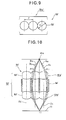
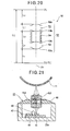
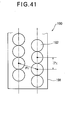
- FIG. 16 is a plan view of a lens array according to the second embodiment of the present invention.
- FIGS. 17 and 18 are a longitudinal sectional view and a cross sectional view of the lens array according to the second embodiment of the present invention.
- the lens array 50 includes four lens plates 51a, 51b, 51c and 51d and a light-blocking portion 54 having a plurality of openings 55.
- the lens plates 51a and 51c are overlapped with each other in the direction of the optical axes Ax, and the lens plates 51b and 51d are overlapped with each other in the direction of the optical axes Ax.
- the light-blocking portion 54 is disposed between the light-blocking portions 51c and 51d.
- a plurality of micro lenses 53 are arranged on predetermined positions of the lens plates 51a through 51d (in this example, on the center portions of each of the lens plates 51a through 51d in the width direction).
- the micro lenses 53 are linearly arranged in the direction perpendicular to the optical axes Ax, i.e., in the longitudinal direction of the lens plates 51a through 51d.
- each of the micro lenses 53 of the lens plate 51a and the corresponding one of the micro lenses 53 of the lens plate 51b constitute a compound lens 61.
- Each of the micro lenses 53 of the lens plates 51b and the corresponding one of the micro lenses 51d constitute a compound lens 61.
- the compound lenses 61 constitute a lens-pair (i.e., a lens group) 62.
- the diameters D1 and D2 are not same as each other.
- the diameters D1 and D2 and the arrangement interval P satisfy: P ⁇ D1, and P ⁇ D2.
- FIG. 19 is a cross sectional view showing a reading apparatus according to the third embodiment of the present invention.
- the reading apparatus 70 is configured to read a manuscript (not shown) and to generate electronic data.
- the reading apparatus 70 includes the lens array 50 (as an optical system) for forming a focused image of the manuscript at a predetermined position, light receiving elements 71 that receive the focused image and convert the focused image into electric signal, a wiring board 72 on which the light receiving elements 71 and a not shown control unit (adjacent to the light receiving elements 71) are disposed, a light source 73 that emits light to the manuscript, a manuscript table 75 made of material that transmits the light (emitted by the light source 73) on which the manuscript is placed, and the like.
- the reference numeral 74 indicates a holding member that holds respective components of the reading apparatus 70.
- FIG. 20 is a schematic view showing an arrangement of optical elements of the reading apparatus according to the third embodiment.
- the mark L 0 indicates the distance between the lens array 50 and the manuscript (i.e., the distance between an object plane and a lens surface), and is defined by the distance between the apex of the outer curved surface 53a of the lens array 50 and a plane (i.e., an object plane P1) on which the manuscript is placed.
- the mark L I indicates the distance between the lens array 50 and the light receiving elements 71 (i.e., the distance between an image plane and a lens surface), and is defined by the distance between the apex of the outer curved surface 53a of the micro lens 53 and a plane (i.e., an image plane P2) on which the light receiving elements 71 are arranged.
- the mark L T indicates the lens thickness, and is defined by the distance between the outer curved surface 53a and the inner curved surface 53b of the micro lens 53.
- the mark L S indicates the lens surface distance, and is defined by the distance between the respective inner curved surfaces 53b of the micro lenses 53 of the lens-pair 52.
- the mark TC indicates the distance between the image plane P2 and the object plane P1, and is defined by distance between the manuscript and the light receiving portion 71.
- the reading apparatus 70 of the third embodiment uses the lens array 50, and the reading apparatus of the comparative example uses the lens array 50' (FIGS. 9 and 10).
- the configurations of the lens array 50 and the lens array 50' are the same as those shown in TABLE 1 described in the first embodiment.
- the light emitted by the light source 73 is reflected by the surface of the manuscript placed on the manuscript table 75.
- the lens array 50 focuses a part of the light reflected by the manuscript, and forms a focused image on a surface of the light receiving elements 71.
- the light receiving elements 71 transfer the focused image into the electric signal.
- the electric signal is sent to the not shown control unit of the reading apparatus 70, and an image data is generated at an image forming portion of the control unit.
- the image data is generated from the same manuscript using the reading apparatus 70 of the third embodiment, and using the reading apparatus of the comparative example.
- the reading apparatus 70 of the third embodiment it is found that the image data similar to the manuscript can be obtained.
- the reading apparatus of the comparative example it is found that stripes occur with a cycle of 1.6 mm which is the same as the arrangement interval P of the micro lenses 53.
- the medium with "1 ⁇ 1" image of 600 dpi (as shown in FIG. 15) is used as the manuscript.
- the third embodiment of the present invention it becomes possible to prevent the degradation of the resolution and the reduction of the amount of light (that otherwise occur with a cycle corresponding to the arrangement interval P of the micro lenses 53 of the reading apparatus 70). Therefore, it becomes possible to prevent the generation of the streaks, stripes or the like on the image data. Accordingly, the image quality can be enhanced, and the image data similar to the manuscript can be obtained.
- FIG. 21 is a cross sectional view of an LED head according to the fourth embodiment of the present invention.
- the LED head 23 includes a lens array 150.
- the lens array 150 is fixed to a supporting body 23a by means of a holding member 46.
- the LED head 23 includes light emitting portions 41 that emit lights to the photosensitive drum 11.
- the light emitting portions 41 include a plurality of LED elements (i.e., light emitting elements) linearly arranged. In this example, the number of the LED elements per inch (approximately 25.4 mm) is 1200.
- a light-blocking portion (not shown) is disposed between the light emitting portions 41 and the lens array 150.
- the light emitting portions 41 and a driver IC 42 for controlling the light emission of the LED elements of the light emitting portions 41 are provided on a wiring substrate 44 (disposed on the supporting body 23a).
- the light emitting portions 41 and the driver IC 42 are connected with each other by means of wires 43.
- the above described control unit generates control signal for the LED head 23 in accordance with the image data, and sends the control signal to the driver IC 42.
- the driver IC 42 causes the LED elements of the light emitting portions 41 to respectively emit lights of predetermined amounts according to the control signal. Then, the lights emitted by the respective LED elements are incident on the lens array 150, pass through the lens array 150 and are focused on the photosensitive drum 11, so that the focused images of the light emitting portion 41 are formed on the photosensitive drum 11.
- the lens array 150 will be described.
- FIGS. 22 and 23 are a perspective view and a partially cutaway plan view of the lens array 150 according to the fourth embodiment of the present invention.
- FIG. 24 is a cross sectional view of the lens array 150.
- the lens array 150 includes two lens plates 151a and 151b arranged in two stages so that the lens plates 151a and 151b face each other.
- Each of the lens plates 151a and 151b includes a plurality of micro lenses 152 having a predetermined curved surfaces.
- the lens array further includes a light-blocking portion 154 made of light-blocking material and disposed between the lens plates 151a and 151b.
- the light-blocking portion 154 has openings 155 corresponding to the micro lenses 152.
- the light-blocking portion 154 shields each pair of micro lenses 152 (facing each other) from the light having passed through any of other pairs of the micro lenses.
- the micro lenses 152 on each of the lens plates 151a and 151b are arranged in at least two rows (in this example, two rows) and arranged in a staggered manner.
- the arrangement interval P Y indicates the interval of the micro lenses 152 in the arranging direction (i.e., the direction in which the micro lenses 152 are arranged in each row).
- the arrangement interval P N indicates the interval (center-to-center distance) between the closest two micro lenses 152 across the rows.
- the arrangement interval P N (i.e., the interval between the closest two micro lenses 152 across the rows) is smaller than the arrangement interval P Y of the micro lenses 152 in the arranging direction. Since the arrangement interval P N is small, the resolution can be enhanced, and the amount of light can be increased.
- each of the micro lenses 152 of the lens plate 151a and the corresponding one of the micro lenses 152 of the lens plate 151b are arranged in two stages so that the optical axes thereof are aligned with each other, and constitute a lens-pair (i.e., a lens group).
- the light-blocking portion 154 includes comb-like members 113a and 113b facing each other in the width direction of the lens plates 151a and 151b, and a partition plate 113 disposed between the comb-like members 113a and 113b.
- the above described openings 155 are formed on the comb-like members 113a and 113b.
- the micro lenses 152 of the lens plates 151a and 151b and the openings 155 of the light-blocking portion 154 are arranged at the same arrangement interval in the same direction (i.e., in the longitudinal direction of the lens plates 151a and 151b).
- the optical axes of the micro lenses 152 of the lens plates 151a and 151b are aligned with the centers of the openings 55.
- Each of the micro lenses 152 is configured to form an inverted image.
- the lens-pair i.e., a pair of micro lenses 152 facing each other
- the arrangement interval of the micro lenses 152 of the lens plates 151a and 151b and the openings 155 of the light-blocking portion 154 is referred to as an arrangement interval P Y (FIG. 23).
- the interval (i.e., center-to-center distance) between the closest micro lenses 152 is referred to as an arrangement interval P N .
- the arrangement intervals P Y and P N satisfy the relationship: P Y > P N
- a row-center-to-array-center distance P A (FIG. 23).
- the lens array 150 of the specific example of the fourth embodiment is prepared for the verification of an advantage of the fourth embodiment.
- the arrangement interval P Y is 1.200 mm and the arrangement interval P N is 1.000 mm.
- the row-center-to-array-center distance P A is 0.400 mm according to the above described equation (3).
- the lens array of comparative example i.e., the lens array 150' shown in FIG. 27
- the arrangement interval P Y is 1.200 mm
- the arrangement interval P N is 1.200 mm
- the row-center-to-array-center distance P A is 0.520 mm according to the above described equation (3).
- the lens array 150 of the specific example of the fourth embodiment and the lens array 150' of the comparative example are different in the positional relationship between the micro lenses 152 and the light emitting portions 41 (FIG. 21). Therefore, the optimum shape of the curved surface of the micro lens 152 of the lens array 150 of the fourth embodiment is different from that of the lens array 150' of the comparative example.
- the lens plates 51a and 51b are formed of cycloolefin-based resin "ZEONEX E48R" (product name) manufactured by Nihon Zeon Corporation.
- the micro lenses 152 are integrally formed with the respective lens plates 151a and 151b by resin molding.
- the light-blocking portion 154 (the comb-like members 113a and 113b) is formed of stainless plates, and the openings 55 are formed by etching.
- a non-reflection coating layer composed of chrome is formed on the surface of the light-blocking portion 154.
- FIG. 25 shows a arrangement of optical elements of the lens array 150 according to the fourth embodiment of the present invention.
- the mark L 0 indicates the distance between the lens array 150 and the light emitting portion 41 (i.e., the distance between an object plane and a lens surface), and is defined by the distance between the apex of the outer curved surface 152a of the micro lens 152 and a plane (i.e., an object plane P1) on which the light emitting portions 41 are arranged.
- the mark L I indicates the distance between the lens array 150 and the photosensitive drum 11 (i.e., the distance between an image plane and a lens surface), and is defined by the distance between the apex of the outer curved surface 152a of the micro lens 152 and a plane (i.e., an image plane P2) on which the photosensitive drum 11 is disposed.
- the mark L T indicates the lens thickness, and is defined by the distance between the outer curved surface 152a and the inner curved surface 152b of the micro lens 152.
- the mark L S indicates the distance between lens surfaces, and is defined by the distance between the respective inner curved surfaces 152b of the micro lenses 152.
- the mark TC indicates the distance between the image plane P2 and the object plane P1, and is defined by distance between the photosensitive drum 11 and the light emitting portion 41.
- the mark r L indicates the radius of the micro lens 152, and the mark r A indicates the radius of the opening 155 (i.e., the opening dimension of the light-blocking portion 154).
- outer curved surface 152a and the inner curved surface 152b of the micro lens 152 are respectively rotationally-symmetric high-order aspheric surfaces, and are respectively expressed as the following equations (4) and (5) :
- Z O r r 2 C O 1 + 1 - r C O 2 + A O ⁇ r 4 + B O ⁇ r 6
- Z I r r 2 C I 1 + 1 - r C I 2 + A I ⁇ r 4 + B I ⁇ r 6
- the above described rotationally-symmetric high-order aspheric surface is a curved surface having the same shape in every radial direction about the optical axis of the micro lens 152 (i.e., rotationally-symmetric shape) and having a plurality of inflection points.
- Each of the functions Z O (r) and Z I (r) indicates a rotating coordinate system whose axis is parallel to the optical axis of the micro lens 152 and in which the radial coordinate is expressed as "r".
- the apexes of the outer curved surface 152a and the inner curved surface 152b of the micro lens 152 are defined as original points.
- the direction from the object plane toward the image plane is expressed as being positive number.
- the mark C o indicates a radius of curvature of the outer curved surface 152a.
- the mark A o indicates a fourth-order aspherical coefficient of the outer curved surface 152a.
- the mark B o indicates a sixth-order aspherical coefficient of the outer curved surface 152a.
- the mark C I indicates a radius of curvature of the inner curved surface 152b.
- the mark A I indicates a fourth-order aspherical coefficient of the inner curved surface 152b.
- the mark B I indicates a sixth-order aspherical coefficient of the inner curved surface 152b.
- micro lenses 152 are integrally formed with the lens plates 151a and 151b in this embodiment, it is also possible to individually form the micro lenses 152 and to fix the micro lenses 152 to the lens plates 151a and 151b at predetermined intervals.
- the outer curved surface 152a and the inner curved surface 152b have rotationally-symmetric high-order aspheric surfaces in this embodiment, the outer curved surface 152a and the inner curved surface 152b can be spherical surfaces. Moreover, the outer curved surface 152a and the inner curved surface 152b can be conic surfaces (such as paraboloidal surfaces, ellipsoidal surfaces, hyperboloidal surfaces or the like), toroidal surfaces (asymmetric in the respective directions perpendicular to the optical axis) and cylindrical surfaces or the like. Further, the outer curved surface 152a and the inner curved surface 152b can be conventional free curved surfaces.
- the outer and inner curved surfaces 152a and 152b are formed as aspherical surfaces, the aberration can be smaller than the micro lens having spherical surfaces, and therefore the resolution can be enhanced. Further, since the outer and inner curved surfaces 152a and 152b are formed to be rotationally-symmetric, the structure of the micro lens 152 can be simpler than the micro lens having asymmetrical surfaces.
- micro lens 152 of this embodiment is composed of as a single lens having two refracting surfaces (curved surfaces), it is also possible to use a compound lens (i.e., a combination of a plurality of single lenses) having four or more refracting surfaces.
- the micro lens 152 is formed of a transparent material (transmitting the light from the light source) having a uniform refractive index and having predetermined curved surfaces. However, it is also possible to use a lens, optical fibers or the like having a predetermined distribution of the refractive index.
- the light-blocking portion 154 is formed of stainless steel plate, it is also possible to form a light-blocking pattern of a light-blocking material (that blocks the light emitted by the light source) on a material that transmits the light. It is also possible to form the light-blocking pattern of the light-blocking material partially on the lens plates 151a and 151b. It is also possible to partially roughen the surfaces of the lens plates 151a and 151b to block the light. It is also possible to partially cut down the lens plates 151a and 151b to prevent the incidence of a part of the light.
- the LED elements are used as the light emitting portions 41.
- organic EL elements as the light emitting portions 41.
- semiconductor lasers as the recording head of the printer 10.
- a light source such as a fluorescent lamp, halogen lamp or the like together with a shutter composed of a liquid crystal display.
- the lens array 150 of this embodiment includes two rows of micro lenses 152, the lens array 150 can have three or more rows of micro lenses 152.
- FIG. 26 shows an optical system of the LED head according to the fourth embodiment of the present invention.
- FIG. 27 shows an optical system of the LED head according to the comparative example.
- FIGS. 26 and 27 a light path between the light emitting portion 41 and an image I focused by the lens array 150 (150') is shown. Further, only one LED element of the light emitting portion 41, two micro lenses 152 of the lens array 150 (150'), the light-blocking portion 154 and the photosensitive drum 11 are shown in FIGS. 26 and 27.
- the horizontal (left-to-right) direction in FIGS. 26 and 27 is the direction of the optical axis between the light emitting portion 41 and the focused image on the photosensitive drum 11.
- the micro lenses 152 and the LED elements are arranged in the direction perpendicular to the sheets of FIGS. 26 and 27.
- FIGS. 26 and 27 only one pair of micro lenses 152 and one opening 55 aligned with each other in the direction of the optical axis are shown in FIGS. 26 and 27.
- the micro lenses 152 of the second row and the corresponding openings 155 of the light-blocking portion 154 are disposed below the micro lenses 152 of the first row and the corresponding openings 155 in a vertically symmetrical manner in FIGS. 26 and 27.
- a light ray traveling along the shortest path of the lens array 150 of the fourth embodiment is defined as a principal ray R M1' and a light ray travelling along the outermost path of the lens array 150 is defined as a rim ray R S1 .
- a light ray traveling along the shortest path of the light path of the lens array 150' of the comparative example is defined as a principal ray R M '
- a light ray travelling along the outermost path of the lens array 150 is defined as a rim ray R S '.
- the angular angle of the light emitted by the light emitting portion 41 of the specific example of the fourth embodiment is referred to as an angular angle ⁇ O1
- the angular angle of the light emitted by the light emitting portion 41 of the comparative example is referred to as an angular angle ⁇ O
- the angular angle of the light incident on the photosensitive drum 11 of the specific example of the fourth embodiment is referred to as an angular angle ⁇ I1
- the angular angle of the light incident on the photosensitive drum 11 of the comparative example is referred to as an angular angle ⁇ I .
- the angular angle of the light emitted by and incident on the respective micro lenses 152 of the specific example of the fourth embodiment is referred to as an angular angle ⁇ L1
- the angular angle of the light emitted by and incident on the respective micro lenses 152 of the comparative example is referred to as an angular angle ⁇ L .
- the angular angles ⁇ O1 , ⁇ I1 and ⁇ L1 of the lens array 150 of the specific example of the fourth embodiment are greater than the angular angles ⁇ O2 , ⁇ I2 and ⁇ L2 of the comparative example. This means that the focused image of the light emitting portion 41 focused by the lens array 150 of the forth embodiment is brighter than the image focused by the lens array 150' of the comparative example.
- the center line of the lens array 150 in the width direction is positioned on a line connecting the light emitting portion 41 and the focused image I focused by the lens array 150.
- the distance between the center line and the optical axis of the micro lens 152 is the above described row-center-to-array-center distance P A .
- the row-center-to-array-center distance P A of the lens array of the specific example of the fourth embodiment is 0.400 mm
- the row-center-to-array-center distance P A of the lens array 150' of the comparative example is 0.520 mm.
- the aberration becomes smaller and the amount of light increases, as the object is closer to the optical axis of the lens.
- the optical axes of the micro lenses 152 are closer to the light emitting portions 41 compared with the lens array 150' of the comparative example. Therefore, it becomes possible to obtain a sharp focused image exhibiting small aberration, and it becomes possible to increase the resolution of the focused image and the amount of light.
- the lens array 150 of the specific example of the fourth embodiment and the lens array 150' of the comparative example are configured as shown in TABLE 2. TABLE 2. MARK PROPERTIES EXAMPLE OF 4TH EMBODIMENT COMPARATIVE EXAMPLE P Y ARRANGEMENT INTERVAL OF MICRO LENSES IN ARRANGING DIRECTION (mm) 1.200 1.200 P N ARRANGEMENT INTERVAL BETWEEN CLOSEST MICRO LENSES (mm) 1.000 1.200 P A ROW-CENTER-TO-ARRAY-CENTER DISTANCE (mm) 0.400 0.520 L O DISTANCE BETWEEN OBJECT PLANE AND LENS SURFACE (mm) 2.300 2.300 r L RADIUS OF MICRO LENS (mm) 0.500 0.500 C O RADIUS OF CURVATURE OF OUTER CURVED SURFACE (mm) 0.8645 0.5833 A O 4TH ORDER ASPHERICAL COEFFICIENT OF OUTER CURVED SURFACE
- TABLE 2 shows the MTF at the resolution of 1200 dpi, and the amount of light (I r ) expressed as a relative value relative to the comparative example.
- the MTF Modulation Transfer Function, i.e., amplitude transfer function
- FIG. 28 is a graph showing the distribution of the amount of light according to the fourth embodiment of the present invention.
- the horizontal axis indicates the position on the image plane, and the vertical axis indicates the amount of light.
- numerals 1, 2, 3 and 4 indicate positions corresponding to the light emitting portions 41 that are activated.
- the MTF indicates a resolution of the focused image focused by the LED head 23 (FIG. 21), i.e., a contrast in the amount of light forming the focused images of activated LED elements of the LED head 23.
- a resolution of the focused image focused by the LED head 23 i.e., a contrast in the amount of light forming the focused images of activated LED elements of the LED head 23.
- MTF I max - I min / I max + I min ⁇ 100 %
- I max is a maximum of the amount of light forming the focused image
- I min is a minimum of the amount of light between the focused images adjacent to each other.
- a microscopic digital camera is used to take the focused image at a position distanced from the end surface of the lens array 150 on the image plane side (the photosensitive drum 11 side) by the distance L I . Based on the image taken by the microscopic digital camera, the distribution of the amount of light forming the focused image of the light emitting portion 41 is analyzed, and the MTF and the amount of light are calculated.
- the lens array 150 of the specific example of the fourth embodiment (and the lens array 150' of the comparative example) is mounted on the LED head 23 of the color LED printer having the resolution of 1200 dpi.
- the LED elements arranged at 1200 dpi i.e, 1200 LED elements are arranged per approximately 25.4 mm
- the maximum amount I max and the minimum amount I min of light are measured.
- the MTF is calculated.
- the measurement of the amount of light is performed while all of the LED elements of the LED head 23 are activated, and the amount of light is determined as an average of the amounts of lights emitted by the respective LED elements.
- the amount of light is expressed as a proportion to that of the comparative example. As shown in TABLE 2, when the lens array 150 of the specific example of the fourth embodiment is used, the amount of light becomes 2.2 times the amount of light when the lens array 150' of the comparative example is used, and the amount of light is found to be sufficient for the LED head 23 of a printer. Further, when the lens array 150 of the specific example of the fourth embodiment is used, the MTF is 91 % (i.e., a sufficient value), i.e., not lower than that when the lens array 150' of the comparative example is used. This is because, in the specific example of the fourth embodiment, the row-center-to-array-center distance P A is small, and therefore the resolution is high and the amount of light is large.
- the aspherical shape of the micro lens 152 of the specific example of the fourth embodiment is different from that of comparative example. This is because the relationship between the micro lens 152 and the light emitting portion 141 in the specific example of the fourth embodiment is different from that of the comparative example, since the distance P A is reduced.
- FIG. 29 shows the "1 ⁇ 1" image of 1200 dpi used in the experiment in the fourth embodiment of the present invention.
- the "1 ⁇ 1" image is an image in which dots D are alternately formed at 600 dpi (i.e., at the interval of 0.0212 mm ⁇ 2) in the vertical and horizontal directions on the dot matrix of 1200 dpi.
- the dots D and the blank spaces B are alternately formed in both of the vertical direction and the horizontal direction on the dot matrix of 1200 dpi.
- the arrangement interval P N between the closest micro lenses 152 is smaller than the arrangement interval P Y in the arranging direction of the micro lenses 152, and therefore the resolution can be enhanced and the amount of light can be increased.
- the image can be formed on the sheet according to the print data without causing the density unevenness, streaks, roughness or the like.
- the lens array of the fourth embodiment is applicable to the reading apparatus (as shown in FIG. 19) as described in the third embodiment.
- FIG. 30 is a partially cutaway plan view of a lens array according to the fifth embodiment of the present invention.
- FIG. 31 is a cross sectional view taken along line XXXI-XXXI shown in FIG. 30.
- FIG. 32 shows an arrangement of optical elements of the lens array according to the fifth embodiment of the present invention.
- the lens array 160 includes two lens plates 161a and 161b arranged in two stages so that the lens plates 161a and 161b face each other.
- Each of the lens plates 161a and 161b has a plurality of micro lenses 162 having predetermined curved surfaces.
- the lens array 160 further includes a light-blocking portion 164 disposed between the lens plates 161a and 161b, and is formed of the comb-like members 113a and 113b (FIG. 22) as was described in the fourth embodiment.
- the light-blocking portion 164 has openings 165 disposed corresponding to the micro lenses 162.
- the micro lenses 162 are arranged in two rows in a staggered manner as was described in the fourth embodiment.
- the micro lenses 162 are so shaped that curved surfaces thereof are cut by a plane parallel to the optical axes of the micro lenses 162 in the direction in which the micro lenses 162 are arranged (i.e., the longitudinal direction of the lens plates 161a and 161b). Further, the micro lenses 162 are so shaped that the cutting surfaces of the micro lenses 162 of two rows mate each other.
- the micro lenses 162 of the lens plates 161a and 161b and the openings 165 of the light-blocking portion 164 are arranged at the same arrangement interval.
- the centers of the openings 165 are aligned with the optical axes of the micro lenses 162 of the lens plates 161a and 161b.
- Each of the micro lenses 162 is configured to form an inverted image.
- the lens-pair i.e., a pair of micro lenses 162 facing each other
- Each of the lens plates 161a and 161b is formed by joining two lens plate parts AR1 and AR2 (FIG. 30).
- the lens plate parts AR1 and AR2 are joined each other in the width direction of the lens plates 161a and 161b so that the micro lenses 162 are disposed in a staggered manner.
- the arrangement interval of the micro lenses 162 of the lens plates 161a and 161b and the arrangement interval of the openings 165 of the light-blocking portion 164 are the same as each other, which is referred to as an arrangement interval P Y (FIG. 23).
- the interval (i.e., center-to-center distance) between the closest micro lenses 162 is referred to as an arrangement interval P N2 .
- the arrangement intervals P Y and P N2 satisfy the relationship: P N2 ⁇ P Y .
- the optical axis is defined to be a line connecting through both apexes of the curved surfaces of the micro lens 162.
- the maximum distance from the optical axis to the periphery of each micro lens 162 (i.e., the distance from the optical axis to the circumferential part of the periphery of each micro lens 162) is defined as a radius r L of the micro lens 162.
- the arrangement interval P N2 and the radius r L satisfy: P N2 ⁇ 2r L
- the distance between the center line of each row of the micro lenses 162 and the center line of the lens plate 161a (161b) in the width direction is referred to as a row-center-to-array-center distance P A as shown in FIG. 30.
- the lens array 160 of a specific example of the fifth embodiment is prepared.
- the radius r L is 0.500 mm
- the arrangement interval P Y is 1.200 mm
- the arrangement interval P N2 is 0.721 mm.
- the row-center-to-array-center distance P A is 0.200 mm according to the above described equation (6).
- the lens plates 161a and 161b are formed of cycloolefin-based resin "ZEONEX E48R" (product name) manufactured by Nihon Zeon Corporation.
- the micro lenses 162 are integrally formed on the respective lens plates 161a and 161b by resin molding.
- the micro lens 162 in a cross section perpendicular to the optical axis, substantially has the shape of a circle partially cut off by a straight line distant from the optical axis by 0.2 mm.
- the opening 165 of the light-blocking portion 164 is in the shape of a circle cut off by a straight line. The light-blocking portion 164 prevents the light from passing through outside the micro lenses 162, and also prevents the light from passing through the center portion of the lens array 160 in the width direction.
- the lens array 160 of the specific example of the fifth embodiment and the lens array 150' of the comparative example are configured as shown in TABLE 3.
- TABLE. 3 MARK PROPERTIES EXAMPLE OF 5TH EMBODIMENT P Y ARRANGEMENT INTERVAL OF MICRO LENSES IN ARRANGING DIRECTION(mm) 1.200 P N2 ARRANGEMENT INTERVAL BETWEEN CLOSEST MICRO LENSES(mm) 0.721 P A ROW-CENTER-TO-ARRAY-CENTER DISTANCE IN WIDTH DIRECTION (mm) 0.200 L O DISTANCE BETWEEN OBJECT PLANE TO LENS SURFACE (mm) 2.300 r L RADIUS OF MICRO LENS (mm) 0.500 C O RADIUS OF CURVATURE OF OUTER CURVED SURFACE (mm) 0.6915 A O 4TH ORDER ASPHERICAL COEFFICIENT OF OUTER CURVED SURFACE -0.3150 B O 6TH ORDER
- the respective surfaces of the micro lens 162 are rotationally-symmetric high-order aspheric surfaces, and expressed as the above described equations (4) and (5).
- the micro lens 162 is so shaped that the micro lens 162 is cut off by a plane in the vicinity of the center line of the lens array 160.
- this does not limit the method for forming the micro lens 162.
- it is possible to make a mold of a predetermined shape, and to form the micro lens 162 using a conventional resin molding method without having a step of cutting off the micro lens 162.
- micro lenses 162 are integrally formed with the lens plates 161a and 161b, it is also possible to individually form the micro lenses 162 and to fix the micro lenses 162 to the lens plates 161a and 161b at the predetermined intervals P Y and P N2 .
- the outer and inner curved surfaces 162a and 162b have rotationally-symmetric high-order aspheric surfaces, the outer and inner curved surfaces 162a and 162b can be spherical surfaces.
- outer and inner curved surfaces 162a and 162b can be conic surfaces (such as paraboloidal surfaces, ellipsoidal surfaces, hyperboloidal surfaces or the like), toroidal surfaces (asymmetric in the respective directions perpendicular to the optical axis) and cylindrical surfaces or the like. Further, the outer and inner curved surfaces 162a and 162b can be conventional free curved surfaces.
- micro lens 162 of this embodiment is composed of a single lens having two refracting surfaces (curved surfaces), it is also possible to use a compound lens (a combination of a plurality of single lenses) having four or more refracting surfaces.
- the micro lens 162 is formed of a transparent material (transmitting the light emitted by the light source) having a uniform refractive index and having predetermined curved surfaces, it is also possible to use a lens, optical fibers or the like having a predetermined distribution of the refractive index.
- the light-blocking portion 164 is formed of stainless steel plate, it is also possible to form a light-blocking pattern of a light-blocking material (that blocks the light emitted by the light source) on a material that transmits the light. It is also possible to form the light-blocking pattern of the light-blocking material partially on the lens plates 161a and 161b. It is also possible to partially roughen the surface of the lens plates 161a and 161b to block the light. It is also possible to partially cut down the lens plates 161a and 161b to prevent the incidence of a part of the light.
- FIG. 33 is a view showing an optical system of an LED head according to the specific example of the fifth embodiment of the present invention.
- FIG. 33 shows a light path from the light emitting portion 41 to the focused image I formed by the lens array 160 (FIG. 32).
- FIG. 33 only one LED element of the light emitting portion 41, two micro lenses 162 of the lens array 160, and the photosensitive drum 11 as the image bearing body are shown.
- the horizontal (left-to-right) direction in FIG. 33 is the direction of the optical axis between the light emitting portion 41 and the focused image I on the photosensitive drum 11.
- the micro lenses 162 and the LED elements are arranged in the direction perpendicular to the sheet of FIG. 33.
- micro lenses 162 and the openings 165 of light-blocking portion 164 only one pair of micro lenses 162 and one opening 165 aligned with each other in the direction of the optical axis are shown in FIG. 33.
- the micro lenses 162 of the second row and the corresponding openings 165 of the light-blocking portion 164 are provided below the micro lenses 162 of the first row and the corresponding openings 165 in a vertically symmetrical manner in FIG. 33.
- a light ray traveling along the shortest path of the lens array 160 of the specific example of the fifth embodiment is defined as a principal ray R M2
- a light ray travelling along the outermost path of the micro lens 162 is defined as a rim ray R S2 .
- the angular angle of the light emitted by the light emitting portion 41 of the specific example of the fifth embodiment is referred to as an angular angle ⁇ O2
- the angular angle of the light incident on the photosensitive drum 11 is referred to as an angular angle ⁇ I2
- the angular angle of the light emitted by and incident on the respective micro lenses 162 of the specific example of the fifth embodiment is referred to as an angular angle ⁇ L2 .
- the angular angles ⁇ O2 , ⁇ I2 and ⁇ L2 of the lens array 160 of the specific example of the fifth embodiment are greater than the angular angles of the comparative example. This means that the focused image of the light emitting portion 41 focused by the lens array 160 of the specific example of the fifth embodiment is brighter than the focused image focused by the lens array 150' of the comparative example.
- the center line of the lens array 160 in the width direction is positioned on a line connecting the light emitting portion 41 and the focused image I focused by the lens array 160.
- the distance between the center line of the lens array 160 and the optical axis of the micro lens 162 is the above described row-center-to-array-center distance P A .
- the row-center-to-array-center distance P A of the lens array 160 of the specific example of the fifth embodiment is 0.200 mm
- the row-center-to-array-center distance P A of the lens array 150' of the comparative example is 0.520 mm.
- the aberration becomes smaller and the amount of light increases, as the object is closer to the optical axis of the lens.
- the optical axes of the micro lenses 162 are closer to the light emitting portions 41 compared with the lens array 150' (FIG. 27) of the comparative example. Therefore, when the lens array 160 according to the fifth embodiment is used, it becomes possible to obtain the sharp focused image exhibiting small aberration. Therefore, it becomes possible to enhance the resolution of the focused image and to increase the amount of light.
- the amount of the light is 3.5 times the amount of light when the lens array 150' of the comparative example is used.
- the MTF is 94% (i.e., sufficient value), i.e., not lower than that when the lens array 150' of the comparative example is used.
- the arrangement interval P N2 between the closest micro lenses 162 is shorter than the arrangement interval P Y of the micro lenses 162 in the arranging direction, so that the resolution can be enhanced and the amount of light can be increased.
- the lens array of the fifth embodiment is applicable to the reading apparatus (FIG. 19) as described in the third embodiment.
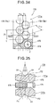
- FIG. 34 is a partially cutaway plan view showing an LED head according to the sixth embodiment of the present invention.
- FIG. 35 is a sectional view taken along line XXXV-XXXV in FIG. 34.
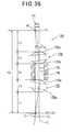
- FIG. 36 shows an arrangement of optical elements of the lens array according to the sixth embodiment of the present invention.
- the lens array 170 includes two lens plates 171a and 171b arranged in two stages so that the lens plates 171a and 171b face each other.
- Each of the lens plates 171a and 171b includes a plurality of micro lenses 172 having predetermined curved surfaces.
- the micro lenses 172 are arranged in two rows and arranged in a staggered manner.
- the lens array further includes light-blocking portion 174 made of light-blocking material and disposed between the lens plates 171a and 171b.
- the light-blocking portion 174 includes a plurality of openings 175 corresponding to the micro lenses 172 of the lens plates 171a and 171b.
- micro lenses 172 of the lens plates 171a and 171b and the openings 175 of the light-blocking portion 174 are arranged at the same arrangement interval.
- the micro lenses 172 include first lenses 172a disposed on the left side of the center line of the lens array 170 in FIG. 34 and second lenses 172b disposed on the right side of the center line of the lens array 170 in FIG. 34.
- the optical axes Ax of first and second lenses 172a and 172b of the lens plate 171a intersect with each other on a predetermined position (in this example, on light emitting portion 41) on the light emitting portion 41 side, i.e., on the object plane side.
- optical axes Ax of first and second lenses 172a and 172b of the lens plate 171b intersect with each other on a predetermined position (in this example, on the photosensitive drum 11) on the photosensitive drum 11 side, i.e., on the image plane side.
- the optical axes Ax are inclined at an angle T (degrees) with respect to the width direction of the lens array 170.
- the arrangement interval of the micro lenses 172 of the lens plates 171a and 171b and the arrangement interval of the openings 175 are the same as each other, which is referred to as an arrangement interval P Y .
- the interval (i.e., center-to-center distance) between the closest micro lenses 172 is referred to as an arrangement interval P N3 .
- the arrangement intervals P Y and P N3 satisfy the relationship: P N3 ⁇ P Y .
- the straight line connecting the apexes of the curved surfaces of the micro lens 172 is defined as the optical axis Ax.
- the distance from the optical axis Ax to the periphery of the micro lens 172 is defined as a radius r L .
- the arrangement interval P N3 and the radius r L satisfy the following relationship: P N3 ⁇ 2r L .
- a row-center-to-array-center distance P A (FIG. 34).
- the lens array 170 of a specific example of the sixth embodiment is prepared.
- the radius r L is 0.500 mm
- the arrangement interval P Y is 1.200 mm
- the arrangement interval P N3 is 0.941 mm.
- the row-center-to-array-center distance P A is 0.362 mm according to the above described equation (7).
- the light-blocking portion 174 of the lens array 170 of the specific example of the sixth embodiment prevents the light from passing through the outside of the micro lenses 172.
- the center C of the opening 175 is distanced from the center of the lens array 170 in the width direction by the distance P S3 (i.e., an opening-center-to-array-center distance).
- the distance P S3 is 0.520 mm.
- the lens array 170 of the specific example of the sixth embodiment and the lens array 150' (FIG. 27) of the comparative example are configured as the following TABLE 4.
- TABLE. 4 MARK PROPERTIES EXAMPLE OF 6TH EMBODIMENT COMPARATIVE EXAMPLE T INCLINATION OF OPTICAL AXIS OF MICRO LENS (degrees) 8.948 0.000 P Y ARRANGEMENT INTERVAL OF MICRO LENSES IN ARRANGING DIRECTION (mm) 1.200 1.200 P N3 ARRANGEMENT INTERVAL BETWEEN CLOSEST MICRO LENSES (mm) 0.941 1.200 P A ROW-CENTER-TO-ARRAY-CENTER DISTANCE IN WIDTH DIRECTION (mm) 0.362 0.520 P S3 OPENING-CENTER-TO-ARRAY-CENTER DISTANCE IN WIDTH DIRECTION (mm) 0.520 0.520 L O DISTANCE BETWEEN OBJECT PLANE TO LENS SURFACE (mm) 2.
- the respective surfaces of the micro lens 172 are rotationally-symmetric high-order aspheric surfaces, and expressed as the above described equations (4) and (5).
- the micro lenses 172 are inclined with respect to the width direction of the lens array 170.
- this does not limit the method for forming the micro lenses 172.
- FIG. 37 shows an optical system of the LED head according to the sixth embodiment.
- FIG. 37 shows a light path from the light emitting portion 41 to the focused image I formed by the lens array 170 (FIG. 35).
- FIG. 37 only one LED element of the light emitting portion 41, two micro lenses 172 of the lens array 170, and the photosensitive drum 11 as the image bearing body are shown.
- the horizontal (left-to-right) direction in FIG. 37 is the direction of the optical axis between the light emitting portion 41 and the focused image on the photosensitive drum 11.
- the micro lenses 172 and the light emitting portions 41 are arranged in the direction perpendicular to the sheet of FIG. 37.
- micro lenses 172 and the openings 175 of light-blocking portion 174 only one pair of micro lenses 172 and one opening 175 aligned with each other in the direction of the optical axes are shown in FIG. 37.
- the micro lenses 172 of the second row and the corresponding openings 175 of the light-blocking portion 174 are disposed below the micro lenses 172 of the first row and the corresponding openings 175 in a vertically symmetrical manner in FIG. 37.
- a light ray traveling along the shortest path of the lens array 170 of the specific example of the sixth embodiment is defined as a principal ray R M3
- a light ray travelling along the outermost path of the micro lens 172 is defined as a rim ray R S3 .
- the angular angle of the light emitted by the light emitting portion 41 of the specific example of the sixth embodiment is referred to as an angular angle ⁇ O3
- the angular angle of the light incident on the photosensitive drum 11 is referred to as an angular angle ⁇ I3
- the angular angle of the light emitted by and incident on the respective micro lenses 162 of the specific example of the sixth embodiment is referred to as an angular angle ⁇ L3 .
- the angular angles ⁇ O3 , ⁇ I3 and ⁇ L3 of the lens array 170 of the specific example of the sixth embodiment are greater than the angular angles of the comparative example (FIG. 27). This means that the focused image of the light emitting portion 41 focused by the lens array 170 of the specific example of the sixth embodiment is brighter than the focused image focused by the lens array 150' of the comparative example.
- the micro lenses 172 are arranged in two rows and since the above described relationship P N3 ⁇ P Y is satisfied, the optical axes of the micro lenses 172 can be disposed closer to the light emitting portion 41.
- the angle T in the following range: 0 ⁇ T ⁇ 2 ⁇ tan -1 P A / L O
- the aberration becomes smaller and the amount of light increases, as the object is closer to the optical axis of the lens.
- the optical axes of the micro lenses 172 are closer to the light emitting portions 41 compared with the lens array 150' of the comparative example. Therefore, when the lens array 170 of the specific example of the sixth embodiment is used, it becomes possible to obtain the sharp focused image exhibiting small aberration. Therefore, it becomes possible to increase the resolution of the focused image and to increase the amount of light.
- the amount of the light is 1.8 times the amount of light when the lens array 150' of the comparative example is used.
- the MTF is 91% (i.e., sufficient value), i.e., not lower than the MTF when the lens array 150' of the comparative example is used.
- the image is formed using the lens array 170 of the specific example of the sixth embodiment, it is found that there is no degradation of the image quality such as a density unevenness (appearing in a high-density region), streaks, roughness or the like.
- the optical axes Ax of the micro lenses 172 are inclined with respect to the width direction of the lens array 170, and therefore the distance P S3 between the center C of the opening 175 of the light-blocking portion 174 and the center of the lens array 170 in width direction is, for example, 0.520 mm.
- the distance P S between the center of the opening 155' and the center of the lens array 150' in the width direction is 0.520 mm (same as the row-center-to-array-center distance P A ). Therefore, the distance P S3 and the distance P S are the same as each other. Since the amount of light can be increased without reducing the distance P S3 , the manufacturing of the lens array 170 of this embodiment is easier than the lens array of the fourth and fifth embodiments.
- the lens array 170 of this embodiment can be easily manufactured.
- the lens array of the sixth embodiment is applicable to the reading apparatus (FIG. 19) as described in the third embodiment.
- FIG. 38 is a partially cutaway plan view showing an LED head according to the seventh embodiment of the present invention.
- FIG. 39 is a sectional view taken along line XXXIX-XXXIX in FIG. 38.
- the lens array 180 includes two lens plates 181a and 181b arranged in two stages so that the lens plates 181a and 181b face each other.
- Each of the lens plates 181a and 181b includes a plurality of micro lenses 182 having predetermined curved surfaces.
- the micro lenses 182 are arranged in two rows and arranged in a staggered manner.
- the lens array further includes a light-blocking portion 184 made of light-blocking material and disposed between the lens plates 181a and 181b.
- the light-blocking portion 184 has a plurality of openings 185 corresponding to the micro lenses 182 of the lens plates 181a and 181b.
- the micro lenses 182 of the lens plates 181a and 181b and the openings 185 of the light-blocking portion 184 are arranged at the same arrangement interval.
- Optical axes Ax of the micro lenses 182 of the lens plate 181a are aligned with the optical axes Ax of the micro lenses 182 of the lens plate 181b.
- the centers C of the openings 185 are disposed outside with respect to the optical axes Ax of the micro lenses 182 in the width direction of the lens array 180.
- the arrangement interval of the micro lenses 182 of the lens plates 181a and 181b and the arrangement interval of the openings 185 in the direction in which the micro lenses 182 are arranged are the same as each other.
- the arrangement interval of the micro lenses 182 is referred to as an arrangement interval P Y
- the interval (i.e., center-to-center distance) between the closest micro lenses 182 is referred to as an arrangement interval P N4 .
- the arrangement intervals P Y and P N4 satisfy: P N4 ⁇ P Y .
- the distance between the center line of each row of the micro lenses 182 and the center line of the lens plate 181a (181b) in the width direction is referred to as a row-center-to-array-center distance P A (FIG. 38).
- the lens array 180 of a specific example of the seventh embodiment is prepared.
- the radius r L is 0.500 mm
- the arrangement interval P Y is 1.200 mm
- the arrangement interval P N4 is 1.000 mm.
- the row-center-to-array-center distance P A is 0.400 mm according to the above described equation (8).
- the centers C of the openings 185 are distanced from the center line of the lens array 180 in the width direction by the distance P S4 (i.e., an opening-center-to-array-center distance).
- the distance P S4 is 0.500 mm.
- the lens array 180 of the specific example of the seventh embodiment and the lens array 150' of the comparative example are configured as the following TABLE 5.
- TABLE. 5 MARK PROPERTIES EXAMPLE OF 7TH EMBODIMENT EXAMPLE OF 4TH EMBODIMENT COMPARATIVE EXAMPLE P Y ARRANGEMENT INTERVAL OF MICRO LENSES IN ARRANGING DIRECTION (mm) 1.200 1.200 1.200 P N4 ARRANGEMENT INTERVAL BETWEEN CLOSEST MICRO LENSES (mm) 1.000 1.000 1.000 P A ROW-CENTER-TO-ARRAY-CENTER DISTANCE IN WIDTH DIRECTION (mm) 0.400 0.400 0.520 L S3 OPENING-CENTER-TO-ARRAY-CENTER DISTANCE IN WIDTH DIRECTION (mm) 2.300 2.300 2.300 r L RADIUS OF MICRO LENS (mm) 0.500 0.500 0.500 C O RADIUS OF CURVATURE OF OUTER CURV
- TABLE 5 also shows the configuration of the lens array 150 (FIG. 23) of the specific example of the fourth embodiment for comparison.
- the respective surfaces of the micro lens 182 are rotationally-symmetric high-order aspheric surfaces, and expressed as the above described equations (4) and (5).
- the centers C of the openings 185 are disposed outside with respect to the optical axes Ax of the micro lenses 182 in the width direction of the lens array 180 in this embodiment, it is only necessary that the light-blocking portion 184 allows a larger amount of light to pass through the outside of the optical axes Ax of the micro lenses 182 in the width direction of the lens array 180.
- the openings 185 of the light-blocking portion 184 can have shapes (for example, an ellipsoidal shape, a drum shape or the like) allowing a larger amount of light to pass through outside of the optical axes Ax of the micro lenses 182 in the width direction of the lens array 180.
- FIG. 40 shows an optical system of the LED head according to the seventh embodiment.
- FIG. 40 shows a light path from the light emitting portion 41 to the focused image I formed by the lens array 180 (FIG. 38).
- FIG. 40 only one LED element of the light emitting portion 41, two micro lenses 182 of the lens array 180, and the photosensitive drum 11 as the image bearing body are shown.
- the horizontal (left-to-right) direction in FIG. 40 is the direction of the optical axis between the light emitting portion 41 and the focused image I on the photosensitive drum 11.
- the micro lenses 182 and the LED elements are arranged in the direction perpendicular to the sheet of FIG. 39.
- micro lenses 182 and the openings 185 of light-blocking portion 184 only one pair of micro lenses 182 and one opening 185 aligned with each other in the direction of the optical axes are shown in FIG. 40.
- the micro lenses 182 of the second row and the corresponding openings 185 of the light-blocking portion 184 are disposed below the micro lenses 182 of the first row and the corresponding openings 185 in a vertically symmetrical manner in FIG. 40.
- a light ray traveling along the shortest path of the lens array 180 of the specific example of the seventh embodiment is defined as a principal ray R M4
- a light ray travelling along the outermost path of the micro lens 182 is defined as a rim ray R S4 .
- the light path between the micro lenses 182 is disposed outside with respect to the optical axes Ax of the micro lenses 182.
- the openings 185 of the light-blocking portion 184 are disposed outside with respect to the optical axes Ax of the micro lenses 182 in the width direction of the lens array 180, the light (including stray light) that may cause aberration is blocked. Therefore, using the lens array 180 of the specific example of the seventh embodiment, it becomes possible to enhance the resolution, compared with the forth, fifth and sixth embodiments. In this case, the decrease in the amount of light is relatively small.
- the amount of light is 2.0 times the amount of light when the lens array 150' of the comparative example is used.
- the sufficient amount of light for the LED head 23 of the printer can be obtained.
- the MTF is 95% (i.e., sufficient value), i.e., not lower than the MTF when the lens array 150' of the comparative example is used.
- the image is formed using the lens array 180 of the specific example of the seventh embodiment, it is found that there is no degradation of the image quality such as a density unevenness (appearing in a high-density region), stripes, roughness or the like.
- the resolution can be enhanced and the decrease in the amount of light can be restricted, compared with the fourth embodiment.
- more excellent resolution and more excellent amount of light can be obtained, compared with the forth embodiment.
- the distance P S4 between the center of the opening 185 and the center of the lens array 180 in the width direction is 0.500 mm
- the row-center-to-array-center distance P A is 0.400 mm. Since the distance between the adjacent openings 185 can be relatively increased, the light-blocking portion 184 can be easily manufactured.
- the resolution can be enhanced, and the amount of light can be increased.
- the lens array of the seventh embodiment is applicable to the reading apparatus (FIG. 19) as described in the third embodiment.
- FIG. 41 is an alternative example of the arrangement of the micro lens 150 (FIG. 23) of the fourth embodiment.
- micro lenses 192 of each lens plate 191 are arranged in two rows and in a staggered manner.
- the arrangement interval P N of the micro lenses 192 in the arranging direction of the micro lenses 192 (the second direction) is smaller than the arrangement interval P Y of the micro lenses 192 in the direction in which the closest micro lenses 192 face each other across the rows (the first direction).
- the arrangement interval P N is small, the resolution can be enhanced, and the amount of light can be increased.
- FIG. 41 can also be applied to the lens array 160 (FIG. 30), the lens array 170 (FIG. 34) and the lens array 180 (FIG. 38).
- the lens array has the micro lenses.
- the present invention is applicable to the lens array having rode lenses.
- the image forming apparatus is not limited to the printer, but can be a copier, a facsimile, a compound apparatus or the like.
- the lenses of the lens array have the same diameter. However, it is also possible that the lenses of the lens array have different diameters.
Landscapes
- Physics & Mathematics (AREA)
- Optics & Photonics (AREA)
- General Physics & Mathematics (AREA)
- Health & Medical Sciences (AREA)
- General Health & Medical Sciences (AREA)
- Toxicology (AREA)
- Printers Or Recording Devices Using Electromagnetic And Radiation Means (AREA)
- Facsimile Heads (AREA)
- Lenses (AREA)
Applications Claiming Priority (2)
| Application Number | Priority Date | Filing Date | Title |
|---|---|---|---|
| JP2006265643A JP2008083576A (ja) | 2006-09-28 | 2006-09-28 | レンズアレイ、露光装置、画像形成装置及び読取装置 |
| JP2006267410A JP4303274B2 (ja) | 2006-09-29 | 2006-09-29 | レンズアレイ、露光装置及び画像形成装置 |
Publications (2)
| Publication Number | Publication Date |
|---|---|
| EP1905602A2 true EP1905602A2 (de) | 2008-04-02 |
| EP1905602A3 EP1905602A3 (de) | 2008-05-14 |
Family
ID=38872059
Family Applications (1)
| Application Number | Title | Priority Date | Filing Date |
|---|---|---|---|
| EP07117136A Ceased EP1905602A3 (de) | 2006-09-28 | 2007-09-25 | Linsenmatrix, Belichtungsvorrichtung, Bilderzeugungsvorrichtung und Lesevorrichtung |
Country Status (2)
| Country | Link |
|---|---|
| US (1) | US7859757B2 (de) |
| EP (1) | EP1905602A3 (de) |
Cited By (1)
| Publication number | Priority date | Publication date | Assignee | Title |
|---|---|---|---|---|
| CN111756948A (zh) * | 2019-03-26 | 2020-10-09 | 富士施乐株式会社 | 光学设备、图像读取设备和图像形成装置 |
Families Citing this family (14)
| Publication number | Priority date | Publication date | Assignee | Title |
|---|---|---|---|---|
| US8085470B2 (en) * | 2008-01-10 | 2011-12-27 | Seiko Epson Corporation | Line head and an image forming apparatus |
| US20090185828A1 (en) * | 2008-01-18 | 2009-07-23 | Seiko Epson Corporation | Lens Array, Exposure Head, and Image Forming Apparatus |
| US8120635B2 (en) * | 2008-01-18 | 2012-02-21 | Seiko Epson Corporation | Exposure head and an image forming apparatus |
| JP2009196345A (ja) * | 2008-01-21 | 2009-09-03 | Seiko Epson Corp | ラインヘッドおよび画像形成装置 |
| TWI370264B (en) * | 2008-06-16 | 2012-08-11 | Univ Nat Sun Yat Sen | Method for manufacturing microlens array |
| JP2010184392A (ja) * | 2009-02-10 | 2010-08-26 | Seiko Epson Corp | ラインヘッドおよび画像形成装置 |
| US9268091B2 (en) * | 2010-02-18 | 2016-02-23 | Corning Cable Systems Llc | Methods for laser processing arrayed optical fibers along with splicing connectors |
| JP6230222B2 (ja) | 2012-10-12 | 2017-11-15 | キヤノン株式会社 | レンズアレイ光学系及びレンズアレイの製造方法 |
| JP6497672B2 (ja) * | 2014-07-16 | 2019-04-10 | Tianma Japan株式会社 | レンズシート及び表示装置並びに電子機器 |
| JP6481381B2 (ja) * | 2015-01-21 | 2019-03-13 | 富士通株式会社 | レンズ間調整方法および光電混載基板 |
| KR20200080838A (ko) * | 2018-12-27 | 2020-07-07 | 에스엘 주식회사 | 차량용 램프 |
| JP7456092B2 (ja) * | 2019-03-26 | 2024-03-27 | 富士フイルムビジネスイノベーション株式会社 | 光学装置、画像読取装置、および画像形成装置 |
| CN111812853B (zh) * | 2019-04-11 | 2025-06-17 | 宁波舜宇光电信息有限公司 | 反射元件、光学准直组件及其制造方法和结构光投射装置 |
| JP7230672B2 (ja) * | 2019-05-07 | 2023-03-01 | コニカミノルタ株式会社 | 露光装置および画像形成装置 |
Citations (8)
| Publication number | Priority date | Publication date | Assignee | Title |
|---|---|---|---|---|
| US3580675A (en) | 1967-11-27 | 1971-05-25 | Agfa Gevaert Ag | Strip scanning copying apparatus |
| JPS56117201A (en) | 1980-02-22 | 1981-09-14 | Ricoh Co Ltd | In-prism lens array |
| US5035486A (en) * | 1980-02-22 | 1991-07-30 | Ricoh Company, Ltd. | Optical imaging apparatus |
| US5163117A (en) | 1989-12-05 | 1992-11-10 | Nippon Sheet Glass Co., Ltd. | Image transmitting element comprising an array of photo-transmissible holes |
| JP2000221445A (ja) | 1999-02-04 | 2000-08-11 | Oki Data Corp | 光学ヘッド用光学系 |
| JP2001249274A (ja) * | 2000-03-02 | 2001-09-14 | Mark:Kk | 迷光を防止した小型レンズアレイ |
| US6366408B1 (en) * | 1999-01-28 | 2002-04-02 | Nippon Sheet Glass Co., Ltd. | Optical imaging system |
| WO2004113967A1 (ja) * | 2003-06-19 | 2004-12-29 | Nippon Sheet Glass Company, Limited | 樹脂性光学部品およびその製造方法 |
Family Cites Families (12)
| Publication number | Priority date | Publication date | Assignee | Title |
|---|---|---|---|---|
| JPS63225218A (ja) | 1987-03-16 | 1988-09-20 | Fujitsu Ltd | 導光レンズアレイ |
| DK300689A (da) * | 1988-06-21 | 1989-12-22 | Rohm Co Ltd | Apparat til optisk skrivning af informationer |
| US5420720A (en) * | 1992-06-25 | 1995-05-30 | Lockheed Missiles & Space Company, Inc. | Internally cooled large aperture microlens array with monolithically integrated microscanner |
| JP3938253B2 (ja) * | 1997-12-26 | 2007-06-27 | 日本板硝子株式会社 | 樹脂正立等倍レンズアレイおよびその製造方法 |
| JP4131891B2 (ja) * | 1999-09-03 | 2008-08-13 | ローム株式会社 | レンズアレイ、およびレンズアレイの製造方法 |
| JP4271841B2 (ja) | 2000-04-05 | 2009-06-03 | ローム株式会社 | レンズアレイユニットおよびこれを備えた光学装置 |
| JP2002107661A (ja) | 2000-10-03 | 2002-04-10 | Nippon Sheet Glass Co Ltd | 線走査用ロッドレンズアレイ |
| JP2003202411A (ja) | 2001-11-01 | 2003-07-18 | Nippon Sheet Glass Co Ltd | 樹脂正立レンズアレイ |
| JP2003302505A (ja) | 2002-04-09 | 2003-10-24 | Ricoh Co Ltd | レンズアレイシート、レンズアレイシート用マスタ、レンズアレイシート用マスタの製造方法、レンズアレイシート用金型、レンズアレイシート用金型の製造方法、スクリーンシート、リアプロジェクションシステム |
| JP4132055B2 (ja) | 2003-07-01 | 2008-08-13 | 日本板硝子株式会社 | 画像読み取り装置 |
| JP2006019918A (ja) | 2004-06-30 | 2006-01-19 | Matsushita Electric Ind Co Ltd | 撮像装置 |
| JP4513653B2 (ja) | 2004-12-27 | 2010-07-28 | 日本ビクター株式会社 | マイクロレンズアレイシートの製造方法 |
-
2007
- 2007-09-25 EP EP07117136A patent/EP1905602A3/de not_active Ceased
- 2007-09-27 US US11/905,023 patent/US7859757B2/en not_active Expired - Fee Related
Patent Citations (9)
| Publication number | Priority date | Publication date | Assignee | Title |
|---|---|---|---|---|
| US3580675A (en) | 1967-11-27 | 1971-05-25 | Agfa Gevaert Ag | Strip scanning copying apparatus |
| JPS56117201A (en) | 1980-02-22 | 1981-09-14 | Ricoh Co Ltd | In-prism lens array |
| US5035486A (en) * | 1980-02-22 | 1991-07-30 | Ricoh Company, Ltd. | Optical imaging apparatus |
| US5163117A (en) | 1989-12-05 | 1992-11-10 | Nippon Sheet Glass Co., Ltd. | Image transmitting element comprising an array of photo-transmissible holes |
| US6366408B1 (en) * | 1999-01-28 | 2002-04-02 | Nippon Sheet Glass Co., Ltd. | Optical imaging system |
| JP2000221445A (ja) | 1999-02-04 | 2000-08-11 | Oki Data Corp | 光学ヘッド用光学系 |
| JP2001249274A (ja) * | 2000-03-02 | 2001-09-14 | Mark:Kk | 迷光を防止した小型レンズアレイ |
| WO2004113967A1 (ja) * | 2003-06-19 | 2004-12-29 | Nippon Sheet Glass Company, Limited | 樹脂性光学部品およびその製造方法 |
| US20070273977A1 (en) * | 2003-06-19 | 2007-11-29 | Nippon Sheet Glass Company, Limited | Resin Optical Member and Method for Manufacturing the Same |
Cited By (1)
| Publication number | Priority date | Publication date | Assignee | Title |
|---|---|---|---|---|
| CN111756948A (zh) * | 2019-03-26 | 2020-10-09 | 富士施乐株式会社 | 光学设备、图像读取设备和图像形成装置 |
Also Published As
| Publication number | Publication date |
|---|---|
| US7859757B2 (en) | 2010-12-28 |
| EP1905602A3 (de) | 2008-05-14 |
| US20080080057A1 (en) | 2008-04-03 |
Similar Documents
| Publication | Publication Date | Title |
|---|---|---|
| US7859757B2 (en) | Lens-array, exposure device, image forming apparatus and reading apparatus | |
| US7706070B2 (en) | Lens array, exposure device, image forming apparatus and LED head | |
| CN101153920A (zh) | 透镜阵列、曝光设备、成像装置以及读取装置 | |
| US8134766B2 (en) | Optical scanning device and image forming apparatus | |
| US8675281B2 (en) | Lens unit, LED head, exposure device, image forming device, and scanning device | |
| US8786656B2 (en) | Lens array, linear light exposure device, and optical apparatus employing the linear light exposure unit | |
| JP4714765B2 (ja) | レンズアレイ、ledプリントヘッド、露光装置、画像形成装置及び読取装置 | |
| JP5584262B2 (ja) | レンズユニット、ledヘッド、露光装置、画像形成装置および読取装置 | |
| US20090086328A1 (en) | Line Head and Image Forming Apparatus Using the Same | |
| US7957067B2 (en) | Lens array, LED head, exposure device, image forming apparatus and reading apparatus | |
| JP4303274B2 (ja) | レンズアレイ、露光装置及び画像形成装置 | |
| US8022975B2 (en) | Line head and image forming apparatus using the same | |
| US10591842B2 (en) | Lens array, lens unit, exposure device, LED head, and image forming apparatus | |
| JP2010184392A (ja) | ラインヘッドおよび画像形成装置 | |
| JP5222161B2 (ja) | レンズユニット、ledヘッド、露光装置、画像形成装置および読取装置 | |
| US20100157429A1 (en) | Lens array, LED head, exposure device, image forming apparatus and reading apparatus | |
| US8184140B2 (en) | Line head and image forming apparatus | |
| US8085455B2 (en) | Optical scanning device, method of adjusting the same, and image forming apparatus | |
| JP2010162850A (ja) | ラインヘッドおよび画像形成装置 | |
| US7710444B2 (en) | Image forming apparatus for forming a latent image on an image carrier | |
| US8179416B2 (en) | Line head and image forming apparatus | |
| JP2010194764A (ja) | ラインヘッドおよび画像形成装置 | |
| JP2009151339A (ja) | レンズアレイ、露光装置、画像形成装置及びledヘッド | |
| JP5797014B2 (ja) | レンズユニット、ledヘッド、画像形成装置および読取装置 | |
| JP2010162852A (ja) | ラインヘッドおよび画像形成装置 |
Legal Events
| Date | Code | Title | Description |
|---|---|---|---|
| PUAI | Public reference made under article 153(3) epc to a published international application that has entered the european phase |
Free format text: ORIGINAL CODE: 0009012 |
|
| AK | Designated contracting states |
Kind code of ref document: A2 Designated state(s): AT BE BG CH CY CZ DE DK EE ES FI FR GB GR HU IE IS IT LI LT LU LV MC MT NL PL PT RO SE SI SK TR |
|
| AX | Request for extension of the european patent |
Extension state: AL BA HR MK YU |
|
| PUAL | Search report despatched |
Free format text: ORIGINAL CODE: 0009013 |
|
| AK | Designated contracting states |
Kind code of ref document: A3 Designated state(s): AT BE BG CH CY CZ DE DK EE ES FI FR GB GR HU IE IS IT LI LT LU LV MC MT NL PL PT RO SE SI SK TR |
|
| AX | Request for extension of the european patent |
Extension state: AL BA HR MK RS |
|
| AKX | Designation fees paid | ||
| 17P | Request for examination filed |
Effective date: 20081029 |
|
| RBV | Designated contracting states (corrected) |
Designated state(s): DE FR GB NL |
|
| RBV | Designated contracting states (corrected) |
Designated state(s): AT BE BG CH CY CZ DE DK EE ES FI FR GB GR HU IE IS IT LI LT LU LV MC MT NL PL PT RO SE SI SK TR |
|
| 17Q | First examination report despatched |
Effective date: 20090114 |
|
| REG | Reference to a national code |
Ref country code: DE Ref legal event code: 8566 |
|
| STAA | Information on the status of an ep patent application or granted ep patent |
Free format text: STATUS: THE APPLICATION HAS BEEN REFUSED |
|
| 18R | Application refused |
Effective date: 20110524 |