EP1905076B1 - Ensemble constitue d'un composant electrique et d'un dispositif de refroidissement a deux phases et procede pour produire cet ensemble - Google Patents
Ensemble constitue d'un composant electrique et d'un dispositif de refroidissement a deux phases et procede pour produire cet ensemble Download PDFInfo
- Publication number
- EP1905076B1 EP1905076B1 EP06764213A EP06764213A EP1905076B1 EP 1905076 B1 EP1905076 B1 EP 1905076B1 EP 06764213 A EP06764213 A EP 06764213A EP 06764213 A EP06764213 A EP 06764213A EP 1905076 B1 EP1905076 B1 EP 1905076B1
- Authority
- EP
- European Patent Office
- Prior art keywords
- component
- evaporator
- cooling device
- arrangement according
- electrical
- Prior art date
- Legal status (The legal status is an assumption and is not a legal conclusion. Google has not performed a legal analysis and makes no representation as to the accuracy of the status listed.)
- Not-in-force
Links
Images
Classifications
-
- H—ELECTRICITY
- H01—ELECTRIC ELEMENTS
- H01L—SEMICONDUCTOR DEVICES NOT COVERED BY CLASS H10
- H01L23/00—Details of semiconductor or other solid state devices
- H01L23/34—Arrangements for cooling, heating, ventilating or temperature compensation ; Temperature sensing arrangements
- H01L23/42—Fillings or auxiliary members in containers or encapsulations selected or arranged to facilitate heating or cooling
- H01L23/427—Cooling by change of state, e.g. use of heat pipes
-
- F—MECHANICAL ENGINEERING; LIGHTING; HEATING; WEAPONS; BLASTING
- F28—HEAT EXCHANGE IN GENERAL
- F28D—HEAT-EXCHANGE APPARATUS, NOT PROVIDED FOR IN ANOTHER SUBCLASS, IN WHICH THE HEAT-EXCHANGE MEDIA DO NOT COME INTO DIRECT CONTACT
- F28D15/00—Heat-exchange apparatus with the intermediate heat-transfer medium in closed tubes passing into or through the conduit walls ; Heat-exchange apparatus employing intermediate heat-transfer medium or bodies
- F28D15/02—Heat-exchange apparatus with the intermediate heat-transfer medium in closed tubes passing into or through the conduit walls ; Heat-exchange apparatus employing intermediate heat-transfer medium or bodies in which the medium condenses and evaporates, e.g. heat pipes
- F28D15/0241—Heat-exchange apparatus with the intermediate heat-transfer medium in closed tubes passing into or through the conduit walls ; Heat-exchange apparatus employing intermediate heat-transfer medium or bodies in which the medium condenses and evaporates, e.g. heat pipes the tubes being flexible
-
- F—MECHANICAL ENGINEERING; LIGHTING; HEATING; WEAPONS; BLASTING
- F28—HEAT EXCHANGE IN GENERAL
- F28D—HEAT-EXCHANGE APPARATUS, NOT PROVIDED FOR IN ANOTHER SUBCLASS, IN WHICH THE HEAT-EXCHANGE MEDIA DO NOT COME INTO DIRECT CONTACT
- F28D15/00—Heat-exchange apparatus with the intermediate heat-transfer medium in closed tubes passing into or through the conduit walls ; Heat-exchange apparatus employing intermediate heat-transfer medium or bodies
- F28D15/02—Heat-exchange apparatus with the intermediate heat-transfer medium in closed tubes passing into or through the conduit walls ; Heat-exchange apparatus employing intermediate heat-transfer medium or bodies in which the medium condenses and evaporates, e.g. heat pipes
- F28D15/04—Heat-exchange apparatus with the intermediate heat-transfer medium in closed tubes passing into or through the conduit walls ; Heat-exchange apparatus employing intermediate heat-transfer medium or bodies in which the medium condenses and evaporates, e.g. heat pipes with tubes having a capillary structure
- F28D15/046—Heat-exchange apparatus with the intermediate heat-transfer medium in closed tubes passing into or through the conduit walls ; Heat-exchange apparatus employing intermediate heat-transfer medium or bodies in which the medium condenses and evaporates, e.g. heat pipes with tubes having a capillary structure characterised by the material or the construction of the capillary structure
-
- F—MECHANICAL ENGINEERING; LIGHTING; HEATING; WEAPONS; BLASTING
- F28—HEAT EXCHANGE IN GENERAL
- F28D—HEAT-EXCHANGE APPARATUS, NOT PROVIDED FOR IN ANOTHER SUBCLASS, IN WHICH THE HEAT-EXCHANGE MEDIA DO NOT COME INTO DIRECT CONTACT
- F28D15/00—Heat-exchange apparatus with the intermediate heat-transfer medium in closed tubes passing into or through the conduit walls ; Heat-exchange apparatus employing intermediate heat-transfer medium or bodies
- F28D15/02—Heat-exchange apparatus with the intermediate heat-transfer medium in closed tubes passing into or through the conduit walls ; Heat-exchange apparatus employing intermediate heat-transfer medium or bodies in which the medium condenses and evaporates, e.g. heat pipes
- F28D15/06—Control arrangements therefor
-
- F—MECHANICAL ENGINEERING; LIGHTING; HEATING; WEAPONS; BLASTING
- F28—HEAT EXCHANGE IN GENERAL
- F28F—DETAILS OF HEAT-EXCHANGE AND HEAT-TRANSFER APPARATUS, OF GENERAL APPLICATION
- F28F13/00—Arrangements for modifying heat-transfer, e.g. increasing, decreasing
- F28F13/18—Arrangements for modifying heat-transfer, e.g. increasing, decreasing by applying coatings, e.g. radiation-absorbing, radiation-reflecting; by surface treatment, e.g. polishing
- F28F13/185—Heat-exchange surfaces provided with microstructures or with porous coatings
- F28F13/187—Heat-exchange surfaces provided with microstructures or with porous coatings especially adapted for evaporator surfaces or condenser surfaces, e.g. with nucleation sites
-
- H—ELECTRICITY
- H01—ELECTRIC ELEMENTS
- H01L—SEMICONDUCTOR DEVICES NOT COVERED BY CLASS H10
- H01L23/00—Details of semiconductor or other solid state devices
- H01L23/34—Arrangements for cooling, heating, ventilating or temperature compensation ; Temperature sensing arrangements
- H01L23/36—Selection of materials, or shaping, to facilitate cooling or heating, e.g. heatsinks
- H01L23/373—Cooling facilitated by selection of materials for the device or materials for thermal expansion adaptation, e.g. carbon
- H01L23/3735—Laminates or multilayers, e.g. direct bond copper ceramic substrates
-
- H—ELECTRICITY
- H01—ELECTRIC ELEMENTS
- H01L—SEMICONDUCTOR DEVICES NOT COVERED BY CLASS H10
- H01L24/00—Arrangements for connecting or disconnecting semiconductor or solid-state bodies; Methods or apparatus related thereto
- H01L24/01—Means for bonding being attached to, or being formed on, the surface to be connected, e.g. chip-to-package, die-attach, "first-level" interconnects; Manufacturing methods related thereto
- H01L24/18—High density interconnect [HDI] connectors; Manufacturing methods related thereto
- H01L24/23—Structure, shape, material or disposition of the high density interconnect connectors after the connecting process
- H01L24/24—Structure, shape, material or disposition of the high density interconnect connectors after the connecting process of an individual high density interconnect connector
-
- H—ELECTRICITY
- H01—ELECTRIC ELEMENTS
- H01L—SEMICONDUCTOR DEVICES NOT COVERED BY CLASS H10
- H01L24/00—Arrangements for connecting or disconnecting semiconductor or solid-state bodies; Methods or apparatus related thereto
- H01L24/80—Methods for connecting semiconductor or other solid state bodies using means for bonding being attached to, or being formed on, the surface to be connected
- H01L24/82—Methods for connecting semiconductor or other solid state bodies using means for bonding being attached to, or being formed on, the surface to be connected by forming build-up interconnects at chip-level, e.g. for high density interconnects [HDI]
-
- H—ELECTRICITY
- H01—ELECTRIC ELEMENTS
- H01L—SEMICONDUCTOR DEVICES NOT COVERED BY CLASS H10
- H01L2224/00—Indexing scheme for arrangements for connecting or disconnecting semiconductor or solid-state bodies and methods related thereto as covered by H01L24/00
- H01L2224/01—Means for bonding being attached to, or being formed on, the surface to be connected, e.g. chip-to-package, die-attach, "first-level" interconnects; Manufacturing methods related thereto
- H01L2224/18—High density interconnect [HDI] connectors; Manufacturing methods related thereto
- H01L2224/23—Structure, shape, material or disposition of the high density interconnect connectors after the connecting process
- H01L2224/24—Structure, shape, material or disposition of the high density interconnect connectors after the connecting process of an individual high density interconnect connector
- H01L2224/2401—Structure
- H01L2224/2402—Laminated, e.g. MCM-L type
-
- H—ELECTRICITY
- H01—ELECTRIC ELEMENTS
- H01L—SEMICONDUCTOR DEVICES NOT COVERED BY CLASS H10
- H01L2224/00—Indexing scheme for arrangements for connecting or disconnecting semiconductor or solid-state bodies and methods related thereto as covered by H01L24/00
- H01L2224/01—Means for bonding being attached to, or being formed on, the surface to be connected, e.g. chip-to-package, die-attach, "first-level" interconnects; Manufacturing methods related thereto
- H01L2224/18—High density interconnect [HDI] connectors; Manufacturing methods related thereto
- H01L2224/23—Structure, shape, material or disposition of the high density interconnect connectors after the connecting process
- H01L2224/24—Structure, shape, material or disposition of the high density interconnect connectors after the connecting process of an individual high density interconnect connector
- H01L2224/2405—Shape
- H01L2224/24051—Conformal with the semiconductor or solid-state device
-
- H—ELECTRICITY
- H01—ELECTRIC ELEMENTS
- H01L—SEMICONDUCTOR DEVICES NOT COVERED BY CLASS H10
- H01L2224/00—Indexing scheme for arrangements for connecting or disconnecting semiconductor or solid-state bodies and methods related thereto as covered by H01L24/00
- H01L2224/01—Means for bonding being attached to, or being formed on, the surface to be connected, e.g. chip-to-package, die-attach, "first-level" interconnects; Manufacturing methods related thereto
- H01L2224/18—High density interconnect [HDI] connectors; Manufacturing methods related thereto
- H01L2224/23—Structure, shape, material or disposition of the high density interconnect connectors after the connecting process
- H01L2224/24—Structure, shape, material or disposition of the high density interconnect connectors after the connecting process of an individual high density interconnect connector
- H01L2224/241—Disposition
- H01L2224/24151—Connecting between a semiconductor or solid-state body and an item not being a semiconductor or solid-state body, e.g. chip-to-substrate, chip-to-passive
- H01L2224/24221—Connecting between a semiconductor or solid-state body and an item not being a semiconductor or solid-state body, e.g. chip-to-substrate, chip-to-passive the body and the item being stacked
- H01L2224/24225—Connecting between a semiconductor or solid-state body and an item not being a semiconductor or solid-state body, e.g. chip-to-substrate, chip-to-passive the body and the item being stacked the item being non-metallic, e.g. insulating substrate with or without metallisation
- H01L2224/24226—Connecting between a semiconductor or solid-state body and an item not being a semiconductor or solid-state body, e.g. chip-to-substrate, chip-to-passive the body and the item being stacked the item being non-metallic, e.g. insulating substrate with or without metallisation the HDI interconnect connecting to the same level of the item at which the semiconductor or solid-state body is mounted, e.g. the item being planar
-
- H—ELECTRICITY
- H01—ELECTRIC ELEMENTS
- H01L—SEMICONDUCTOR DEVICES NOT COVERED BY CLASS H10
- H01L2224/00—Indexing scheme for arrangements for connecting or disconnecting semiconductor or solid-state bodies and methods related thereto as covered by H01L24/00
- H01L2224/80—Methods for connecting semiconductor or other solid state bodies using means for bonding being attached to, or being formed on, the surface to be connected
- H01L2224/82—Methods for connecting semiconductor or other solid state bodies using means for bonding being attached to, or being formed on, the surface to be connected by forming build-up interconnects at chip-level, e.g. for high density interconnects [HDI]
- H01L2224/82009—Pre-treatment of the connector or the bonding area
- H01L2224/8203—Reshaping, e.g. forming vias
- H01L2224/82035—Reshaping, e.g. forming vias by heating means
- H01L2224/82039—Reshaping, e.g. forming vias by heating means using a laser
-
- H—ELECTRICITY
- H01—ELECTRIC ELEMENTS
- H01L—SEMICONDUCTOR DEVICES NOT COVERED BY CLASS H10
- H01L2924/00—Indexing scheme for arrangements or methods for connecting or disconnecting semiconductor or solid-state bodies as covered by H01L24/00
- H01L2924/01—Chemical elements
- H01L2924/01005—Boron [B]
-
- H—ELECTRICITY
- H01—ELECTRIC ELEMENTS
- H01L—SEMICONDUCTOR DEVICES NOT COVERED BY CLASS H10
- H01L2924/00—Indexing scheme for arrangements or methods for connecting or disconnecting semiconductor or solid-state bodies as covered by H01L24/00
- H01L2924/01—Chemical elements
- H01L2924/01006—Carbon [C]
-
- H—ELECTRICITY
- H01—ELECTRIC ELEMENTS
- H01L—SEMICONDUCTOR DEVICES NOT COVERED BY CLASS H10
- H01L2924/00—Indexing scheme for arrangements or methods for connecting or disconnecting semiconductor or solid-state bodies as covered by H01L24/00
- H01L2924/01—Chemical elements
- H01L2924/01013—Aluminum [Al]
-
- H—ELECTRICITY
- H01—ELECTRIC ELEMENTS
- H01L—SEMICONDUCTOR DEVICES NOT COVERED BY CLASS H10
- H01L2924/00—Indexing scheme for arrangements or methods for connecting or disconnecting semiconductor or solid-state bodies as covered by H01L24/00
- H01L2924/01—Chemical elements
- H01L2924/01023—Vanadium [V]
-
- H—ELECTRICITY
- H01—ELECTRIC ELEMENTS
- H01L—SEMICONDUCTOR DEVICES NOT COVERED BY CLASS H10
- H01L2924/00—Indexing scheme for arrangements or methods for connecting or disconnecting semiconductor or solid-state bodies as covered by H01L24/00
- H01L2924/01—Chemical elements
- H01L2924/01029—Copper [Cu]
-
- H—ELECTRICITY
- H01—ELECTRIC ELEMENTS
- H01L—SEMICONDUCTOR DEVICES NOT COVERED BY CLASS H10
- H01L2924/00—Indexing scheme for arrangements or methods for connecting or disconnecting semiconductor or solid-state bodies as covered by H01L24/00
- H01L2924/01—Chemical elements
- H01L2924/01033—Arsenic [As]
-
- H—ELECTRICITY
- H01—ELECTRIC ELEMENTS
- H01L—SEMICONDUCTOR DEVICES NOT COVERED BY CLASS H10
- H01L2924/00—Indexing scheme for arrangements or methods for connecting or disconnecting semiconductor or solid-state bodies as covered by H01L24/00
- H01L2924/01—Chemical elements
- H01L2924/01074—Tungsten [W]
-
- H—ELECTRICITY
- H01—ELECTRIC ELEMENTS
- H01L—SEMICONDUCTOR DEVICES NOT COVERED BY CLASS H10
- H01L2924/00—Indexing scheme for arrangements or methods for connecting or disconnecting semiconductor or solid-state bodies as covered by H01L24/00
- H01L2924/01—Chemical elements
- H01L2924/01082—Lead [Pb]
-
- H—ELECTRICITY
- H01—ELECTRIC ELEMENTS
- H01L—SEMICONDUCTOR DEVICES NOT COVERED BY CLASS H10
- H01L2924/00—Indexing scheme for arrangements or methods for connecting or disconnecting semiconductor or solid-state bodies as covered by H01L24/00
- H01L2924/013—Alloys
- H01L2924/014—Solder alloys
-
- H—ELECTRICITY
- H01—ELECTRIC ELEMENTS
- H01L—SEMICONDUCTOR DEVICES NOT COVERED BY CLASS H10
- H01L2924/00—Indexing scheme for arrangements or methods for connecting or disconnecting semiconductor or solid-state bodies as covered by H01L24/00
- H01L2924/10—Details of semiconductor or other solid state devices to be connected
- H01L2924/11—Device type
- H01L2924/13—Discrete devices, e.g. 3 terminal devices
- H01L2924/1301—Thyristor
-
- H—ELECTRICITY
- H01—ELECTRIC ELEMENTS
- H01L—SEMICONDUCTOR DEVICES NOT COVERED BY CLASS H10
- H01L2924/00—Indexing scheme for arrangements or methods for connecting or disconnecting semiconductor or solid-state bodies as covered by H01L24/00
- H01L2924/10—Details of semiconductor or other solid state devices to be connected
- H01L2924/11—Device type
- H01L2924/13—Discrete devices, e.g. 3 terminal devices
- H01L2924/1304—Transistor
- H01L2924/1305—Bipolar Junction Transistor [BJT]
- H01L2924/13055—Insulated gate bipolar transistor [IGBT]
-
- H—ELECTRICITY
- H01—ELECTRIC ELEMENTS
- H01L—SEMICONDUCTOR DEVICES NOT COVERED BY CLASS H10
- H01L2924/00—Indexing scheme for arrangements or methods for connecting or disconnecting semiconductor or solid-state bodies as covered by H01L24/00
- H01L2924/10—Details of semiconductor or other solid state devices to be connected
- H01L2924/11—Device type
- H01L2924/13—Discrete devices, e.g. 3 terminal devices
- H01L2924/1304—Transistor
- H01L2924/1306—Field-effect transistor [FET]
- H01L2924/13091—Metal-Oxide-Semiconductor Field-Effect Transistor [MOSFET]
-
- Y—GENERAL TAGGING OF NEW TECHNOLOGICAL DEVELOPMENTS; GENERAL TAGGING OF CROSS-SECTIONAL TECHNOLOGIES SPANNING OVER SEVERAL SECTIONS OF THE IPC; TECHNICAL SUBJECTS COVERED BY FORMER USPC CROSS-REFERENCE ART COLLECTIONS [XRACs] AND DIGESTS
- Y10—TECHNICAL SUBJECTS COVERED BY FORMER USPC
- Y10T—TECHNICAL SUBJECTS COVERED BY FORMER US CLASSIFICATION
- Y10T29/00—Metal working
- Y10T29/49—Method of mechanical manufacture
- Y10T29/49002—Electrical device making
- Y10T29/49117—Conductor or circuit manufacturing
- Y10T29/49169—Assembling electrical component directly to terminal or elongated conductor
Definitions
- the invention relates to an arrangement of at least one electrical component and at least one cooling device for dissipating heat from the component, wherein the cooling device has at least one two-phase cooling device with at least one evaporator and the evaporator has a structured evaporator surface for evaporating a cooling fluid.
- a method for producing the device is specified.
- Object of the present invention is to provide a compact and easy to manufacture arrangement of electrical component and two-phase cooling device.
- an arrangement of at least one electrical component and at least one cooling device for dissipating heat from the component wherein the cooling device has at least one two-phase cooling device with at least one evaporator and the evaporator has a structured evaporator surface for evaporating a cooling fluid.
- the arrangement is characterized in that the structured evaporator surface of a electrical connection line for electrically contacting an electrical contact surface of the device is formed.
- the basic idea of the invention is to design the electrical connection line for the electrical contacting of the component as an evaporator of the two-phase cooling device. Especially in the operation of power devices develop due to the high currents that are transported through the connecting line, large amounts of heat. Because the connecting line itself forms the evaporator surface, these amounts of heat can be derived directly at the point of origin. Many conductor materials, for example copper or aluminum, are not only electrically but also highly thermally conductive, so that in addition an efficient heat conduction path is provided away from the component via the connecting line as evaporator. In addition, the structured evaporator surface results in efficient cooling. The structured evaporator surface has an enlarged evaporator surface available for the evaporation process compared to an unstructured surface (see below).
- the two-phase cooling device in a particular embodiment comprises a condenser with a structured condenser surface for liquefying the cooling fluid.
- the structured condenser surface also has an enlarged condenser surface available for the liquefaction process compared to an unstructured surface.
- the below-described, special embodiments of the structured Evaporator surface may also affect the condenser surface.
- a two-phase cooling device consists essentially of an evaporator (evaporator) for evaporating a cooling fluid, a condenser (condenser) for liquefying the cooling fluid and a fluid channel for transporting the cooling fluid as both liquid and gaseous phase.
- the fluid channel forms a vapor space of the two-phase cooling device, in which the cooling fluid is vaporized at the evaporator. From the steam room, the liquefaction of the cooling fluid takes place at the condenser.
- the two-phase cooling device allows using the evaporation and condensation heat of the cooling fluid (coolant) a high heat flux density.
- the high heat flow density results as follows:
- the evaporator is thermally conductively connected to the electrical component via the electrical connection line.
- the heat generated during operation of the electrical component is transferred to the evaporator.
- the transferred heat leads to the evaporation of the liquid cooling fluid.
- the cooling fluid passes from the liquid phase to the gaseous phase.
- the cooling fluid absorbs heat of vaporization.
- the gaseous cooling fluid passes to the condenser.
- the condenser is thermally conductively connected to a heat sink. In the condenser, condensation of the gaseous cooling fluid occurs.
- the cooling fluid passes from the gaseous phase into the liquid phase. This heat of condensation is released to the heat sink.
- the two-phase cooling device is realized as a boiling bath cooling.
- the evaporator or the evaporator surface is in a cooling fluid bath (boiling bath).
- the evaporator surface and the vapor space are not directly in contact, but indirectly via the liquid cooling fluid in contact.
- the evaporation of the cooling fluid leads to typical vapor bubble formation in the liquid cooling fluid.
- the boiling bath not only serves to accommodate the evaporator or the evaporator surface, but also the recording and the cooling of the entire component.
- an electrically non-conductive, ie electrically insulating cooling fluid is used.
- halogenated and advantageously fluorinated hydrocarbons are used as the cooling fluid.
- the fluorinated hydrocarbon Fluorinert ® is used as the fluorinated hydrocarbon Fluorinert ®.
- the connecting line has, in particular, an electrically and thermally highly conductive metal.
- the metal is in particular copper or aluminum.
- the connecting line for forming the evaporator surface on an electrochemical deposition In particular, the electrochemical deposition on copper. Copper can be deposited in a simple manner and in relatively large layer thicknesses galvanically from a solution containing copper salt. The layer thicknesses can reach up to several 100 ⁇ m. This can be provided for a current carrying capacity necessary for the operation of the component, for example a power semiconductor component.
- the assembly may comprise any electrical component that must be efficiently cooled for stable operation.
- the component is a power semiconductor component.
- the power semiconductor component is selected from the group of IGBT, diode, MOSFET, thyristor and bipolar transistor.
- the component is arranged on a substrate such that the electrical contact surface of the component is turned away from the substrate.
- an efficient heat conduction path is provided away from the component. This efficient heat conduction path does not pass over the substrate.
- a single electrical device for a single substrate.
- a plurality of components are arranged on a substrate (module).
- the components can be wired to each other corresponding connection lines.
- each of the components is thermally conductively connected to one or more two-phase cooling devices.
- the evaporator surface is formed by a plurality of structured connecting lines. This allows efficient heat spreading across the entire substrate. There are no heat peaks. Heat spikes could result in lasting damage to the entire module from the devices and the substrate.
- an electrical insulating film is laminated onto the component and the substrate, so that a surface contour, which is formed by the component and the substrate, in a surface contour of the Insulating film is shown, which is remote from the device and the substrate.
- the surface contour (topography) of the component and the substrate is molded by the insulating film.
- the insulation foil follows the Surface contour of the device and the substrate. This applies in particular to corners and edges of the component and of the substrate.
- a molding of the surface contour of the component and of the substrate is achieved by laminating the insulation film to the component and to the substrate. The lamination results in a particularly intimate and firm contact between the insulating film and the electrical component and between the insulating film and the electrical component.
- the insulating film is laminated under vacuum.
- the connecting line with the structured evaporator surface is applied to the insulating film.
- an insulating film is laminated.
- at least one window in the insulation film is opened. By opening the window, the electrical contact surface of the device is exposed. The opening of the window takes place, for example, by laser ablation or by a photolithographic process.
- electrically conductive conductor material is deposited.
- connection line consists of stacked metallization layers.
- the contact surface of the power semiconductor component consists of aluminum.
- a lowermost metallization layer which is applied directly to the contact surface of the power semiconductor component, consists for example of titanium and acts as an adhesion-promoting layer.
- An overlying metallization layer consists of a titanium-tungsten alloy, which serves as a barrier layer for copper ions acts. The conclusion is a galvanically deposited copper layer. This copper layer is patterned to form the structured evaporator surface. For structuring, in particular a galvanic, mechanical and / or electrochemical structuring is carried out.
- the structure of the evaporator surface is dimensioned such that an efficient evaporation of the cooling fluid is possible.
- the structure is therefore based on the amount of heat that arises during the operation of the device and must be derived.
- the structure depends on the cooling fluid and the conductor material from which the evaporator surface is formed. So it is useful to ensure sufficient wettability. This also applies with regard to the design of the two-phase cooling device as Siedebadkühlung. By sufficient wettability, for example, boiling defects are prevented.
- the structured evaporator surface therefore has a capillary structure. Local hot spots are cooled particularly well by the evaporation process, which allows an isothermal operation of the device.
- the capillary structure has a dimension selected from the range of 0.1 ⁇ m up to and including 1000 ⁇ m and in particular from the range of 10 ⁇ m to 100 ⁇ m inclusive. These dimensions prove to be particularly advantageous.
- the capillary structure has capillaries.
- a capillary is a cavity, in particular a narrow-volume cavity with a dimension from the stated ranges.
- the capillaries represent open surface structures. Through the open Surface structures takes place a transport of the cooling fluid due to capillary forces.
- the capillary structure, the conductor material which forms the capillary structure, and the cooling fluid are matched to one another, so that good wettability of the evaporator surface with the capillary structure by the cooling fluid is ensured. It is particularly advantageous if the evaporator surface with the capillary structure is part of the cooling channel of the two-phase cooling device.
- the two-phase cooling device as a "heat pipe” is provided with this embodiment for efficient transport of the cooling fluid and thus for efficient cooling.
- This embodiment also has the particular advantage that the likelihood of "dry running" the evaporator surface is reduced as compared to another two-phase cooling device.
- the evaporator surface is at least partially no longer wetted by the cooling fluid, which is also referred to as "Leidenfrost phenomenon".
- Leidenfrost phenomenon there is no cooling by evaporation. It can lead to overheating and thus damage to the device or the entire arrangement.
- the structured evaporator surface is thus accompanied by an increase in the critical heat flow density, up to a thermal operation is possible.
- the two-phase cooling device has a means for setting a boiling temperature of the cooling fluid. This is particularly advantageous if the arrangement or the component is operated at different temperatures. Also conceivable are temperature fluctuations occurring during operation. With the means, the different temperatures or temperature fluctuations can be compensated without a cooling performance of the two-phase cooling device would be affected. There is an efficient cooling of the device at any time.
- the means for adjusting the boiling temperature may be, for example, an external pressure generator, which is in contact with the vapor space. Thereby, a vapor pressure of the cooling fluid in the vapor space can be increased or decreased. As a result, the boiling temperature is lowered or increased.
- the means for adjusting the boiling temperature comprises means for varying a vapor space of the two-phase cooling device, which is in contact with the evaporator surface of the evaporator.
- the evaporator surface and the vapor space may be in direct or indirect contact with each other.
- a change of the vapor space includes a change of a vapor space volume of the vapor space.
- the means for changing the steam space in particular a stretchable bellows.
- the bellows has a variable bellows volume.
- the bellows volume can be formed directly from the vapor space. It is also conceivable that a bellows space forming the bellows volume and the vapor space forming the vapor space volume are connected indirectly via a pressure transmission device.
- a pressure transmission device is for example an elastically deformable membrane. A change in the pressure in the bellows space is transferred via the membrane to the vapor space. This can lead to a change in the pressure in the steam space or to a change in the headspace volume.
- an already prefabricated, structured connecting line can be connected to the contact surface of the component.
- the connecting line is not structured until it is already connected to the contact surface of the device. According to a particular embodiment, therefore, the following further method steps are carried out for producing the connecting line: c) applying electrically conductive conductor material and d) structuring the applied electrically conductive conductor material during and / or after the application of the electrically conductive conductor material.
- the application of the electrically conductive conductor material can be carried out from the vapor phase (vapor deposition), for example via PVD (Physical Vapor Deposition) - or CVD (Chemical Vapor Deposition) method.
- the conductor material as described above, electrochemically deposited. The result is the electrochemical deposition.
- the structuring of the surface of the applied conductor material takes place, for example, during the application by using a suitable structuring mask. It is also conceivable structuring by material removal. Preferably, therefore, a galvanic, mechanical and / or electromechanical structuring is used for structuring.
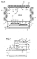
- the exemplary embodiments relate in each case to an arrangement 1 of at least one electrical component 2 and at least one cooling device 3 for dissipating heat which arises during operation of the component 2.
- the electrical component 2 is a power semiconductor component in the form of a MOSFET.
- the power semiconductor device 2 is an IGBT.
- the power semiconductor component 2 is part of an entire module 20, in which a plurality of power semiconductor components 2, not shown, are arranged and wired on a single, common substrate 4.
- the substrate 4 is a DCB (Direct Copper Bonding) substrate.
- a ceramic layer 41 is provided on both sides with copper layers 42 and 42.
- the power semiconductor component 2 has an electrical contact surface 21, which is electrically contacted over a large area.
- the power semiconductor component 2 is soldered on one of the copper layers 42 and 43 of the substrate 4 such that the contact surface 21 of the power semiconductor component 2 to be contacted is turned away from the substrate 4.
- the result is a Lotbahn 22 between the power semiconductor device 2 and the corresponding copper layer 42 of the substrate 4.
- the copper layer 42 and the Lotbahn 22 serve the electrical contacting of a further electrical contact surface 23 of the power semiconductor component 2.
- an electrical insulation film 5 is laminated onto the component 2 and the substrate 4 such that a surface contour 24 formed by the power semiconductor component 2 and the substrate 4 is imaged in the surface contour 51 of the insulation film 5 which is turned away from the power semiconductor device 2 and the substrate 4 (see FIG. FIG. 2 ).
- 2 insulation material of the insulating film 5 is removed in the insulating film 5 to expose the contact surface 21 of the power semiconductor device 2. This is done by laser ablation. The result is a window 52 in the insulating film.
- the contact surface 21 of the power semiconductor component 2 is freely accessible.
- the electrical connection line 6 is applied for making electrical contact with the contact surface 21.
- electrically conductive materials are applied in a structured manner on the contact surface 21 and on a film surface 53 of the insulating film 5, which faces away from the substrate 4 and the power semiconductor component 2.
- the result is a multi-layered electrical connection line 6 of a plurality of electrically conductive layers 61.
- the electrical feedthrough 54 is generated by the insulating film 5.
- the conclusion of the multilayer connecting line 6 forms an electrochemical deposition 62 of copper.
- copper is electrodeposited from a suitable solution with copper ions.
- the cooling device is a two-phase cooling device 3 with an evaporator 31 for a cooling fluid 34.
- the cooling fluid is a Fluorinert®.
- the evaporator 31 has a Evaporator surface 311 on. On the evaporator surface 311 evaporation of the cooling fluid 34 takes place. The evaporation takes place in the vapor space 312 of the two-phase cooling device 3.
- the two-phase cooling device 3 has a condenser 32 for condensing the cooling fluid 34. At a condenser surface 321, the cooling fluid 34 condenses.
- the evaporator 31 or the evaporator surface 311 is immersed in a boiling bath 36 with the cooling fluid 34. There is a boiling bath cooling.
- the two-phase cooling device 3 is designed as a "heat pipe”. By capillary forces, the cooling fluid 33 is transported from the condenser 32 to the evaporator 31.
- the evaporator surface 311 with the capillary structure 313 is part of the fluid channel 33.
- the evaporator 31 is connected to the condenser 32 via the steam space 312.
- the gaseous cooling fluid 34 passes through the vapor space 312 to the condenser 32.
- the vapor space 312 constitutes the fluid channel 33 of the two-phase cooling device 3.
- the condenser 32 is in thermal contact with a heat sink 35.
- the heat sink 35 has a copper block with cooling fins 351. In this way, the condensation heat released in condensing the cooling fluid 34 at the condenser surface 321 is efficiently dissipated.
- the evaporator surface 321 is structured.
- the structured evaporator surface is formed by the electrical connecting line 6 for contacting the electrical contact surface 21 of the component 2.
- the structured evaporator surface 311 has a capillary structure 313. About the capillary 313 is taking advantage of capillary forces constantly liquid or liquefied cooling fluid 34 introduced. In addition, the patterning leads to an enlargement of the effective evaporator surface 311 usable for the evaporation. An efficient cooling of the power semiconductor component 2 occurs.
- the condenser surface 321 is also structured.
- the condenser surface 321 also has a corresponding capillary structure 323 for this purpose.
- the capillary structure 313 copper is deposited in a patterned manner. This succeeds with a suitable structuring mask.
- the capillary structure 313 is electromechanically generated after electrodepositing copper. It is removed copper.
- the capillary structure 323 of the condenser surface is represented in a corresponding manner.
- a means 37 for adjusting the boiling temperature of the cooling fluid 34 is present.
- the boiling temperature adjusting means 37 is a means for changing the steam space 312.
- the vapor space changing means is a stretchable bellows with which the vapor space volume can be changed. Due to the adjustability of the boiling temperature of the cooling fluid 34, heat can be efficiently dissipated at any time, ie independently of the operating phase or the operating state of the power semiconductor component 2 or of the module 20.
Landscapes
- Engineering & Computer Science (AREA)
- Physics & Mathematics (AREA)
- Microelectronics & Electronic Packaging (AREA)
- Power Engineering (AREA)
- General Engineering & Computer Science (AREA)
- Mechanical Engineering (AREA)
- Thermal Sciences (AREA)
- Computer Hardware Design (AREA)
- Sustainable Development (AREA)
- Chemical & Material Sciences (AREA)
- Life Sciences & Earth Sciences (AREA)
- General Physics & Mathematics (AREA)
- Condensed Matter Physics & Semiconductors (AREA)
- Materials Engineering (AREA)
- Ceramic Engineering (AREA)
- Crystallography & Structural Chemistry (AREA)
- Cooling Or The Like Of Semiconductors Or Solid State Devices (AREA)
- Constitution Of High-Frequency Heating (AREA)
- Emergency Protection Circuit Devices (AREA)
Claims (16)
- Ensemble composé d'au moins un composant ( 2 ) électrique et d'un dispositif ( 3 ) de refroidissement, pour évacuer de la chaleur du composant ( 2 ) électrique, dans lequel- le dispositif ( 3 ) de refroidissement comporte au moins un dispositif de refroidissement à deux phases ayant au moins un évaporateur ( 31 ),
caractérisé en ce que- l'évaporateur ( 31 ) a une surface ( 311 ) d'évaporateur structurée pour l'évaporation d'un fluide ( 34 ) de refroidissement,- la surface ( 311 ) d'évaporateur structurée est formée par une ligne ( 6 ) électrique de liaison pour la mise en contact électrique d'une surface ( 21 ) de contact électrique du composant ( 2 ), et- le composant est un composant de puissance à semiconducteur choisi dans le groupe IGBT, diode, MOSFET, thyristor et transistor bipolaire. - Ensemble suivant la revendication 1, dans lequel la surface ( 311 ) d'évaporateur structurée a une structure ( 313 ) capillaire.
- Ensemble suivant la revendication 2, dans lequel la structure ( 313 ) capillaire a une dimension choisie dans une plage allant de y compris 0,1 µm à y compris 1 000 µm et notamment dans la plage allant de y compris 10 µm à y compris 100 µm.
- Ensemble suivant l'une des revendications 1 à 3, dans lequel le dispositif ( 3 ) de refroidissement à deux phases a un moyen ( 37 ) de réglage d'une température d'ébullition du fluide ( 34 ) de refroidissement.
- Ensemble suivant la revendication 4, dans lequel le moyen ( 37 ) de réglage de la température d'ébullition a un moyen de modification d'un espace ( 312 ) de vapeur du dispositif de refroidissement à deux phases, qui est en contact avec la surface ( 311 ) de l'évaporateur ( 31 ).
- Ensemble suivant la revendication 5, dans lequel le moyen de modification de l'espace de vapeur comporte un soufflet extensible.
- Ensemble suivant l'une des revendications 1 à 6, dans lequel la ligne ( 6 ) de liaison a un dépôt ( 62 ) électrochimique pour la formation de la surface ( 311 ) d'évaporateur.
- Ensemble suivant la revendication 4, dans lequel le dépôt ( 62 ) électrochimique comporte du cuivre.
- Ensemble suivant l'une des revendications 1 à 8, dans lequel le dispositif ( 3 ) de refroidissement à deux phases a un condenseur pour condenser le fluide ( 34 ) de refroidissement.
- Ensemble suivant l'une des revendications 1 à 9, dans lequel le dispositif ( 3 ) de refroidissement à deux phases est conformé en refroidissement à bain ébullition ayant un bain ( 36 ) d'ébullition pour la réception du composant ( 2 ).
- Ensemble suivant l'une des revendications 1 à 10, dans lequel le composant ( 2 ) électrique est disposé sur un substrat ( 4 ), de manière à ce que la surface ( 21 ) de contact électrique du composant ( 2 ) soit éloignée du substrat ( 4 ).
- Ensemble suivant la revendication 11, dans lequel une feuille ( 5 ) isolante du point de vue électrique est laminée sur le composant ( 2 ) du substrat ( 4 ), de manière à former un contour ( 24 ) de surface, qui est formé par le composant ( 2 ) et par le substrat ( 4 ) dans un contour ( 51 ) de surface de la feuille ( 5 ) isolante, qui est éloigné du composant ( 2 ) et du substrat ( 4 ).
- Ensemble suivant la revendication 11 ou 12, dans lequel la ligne ( 6 ) de liaison est déposée par la surface ( 311 ) d'évaporateur structurée sur la feuille ( 5 ) isolante et, pour la mise en contact de la surface ( 21 ) de contact électrique du composant ( 2 ), il est prévu un contact ( 54 ) électrique traversant la feuille ( 5 ) isolante.
- Procédé de production d'un ensemble suivant l'une des revendications 1 à 13, comprenant les stades suivants :a) on se procure un composant électrique ayant une surface de contact électrique, le composant ( 2 ) étant un composant de puissance à semiconducteur choisi dans le groupe IGBT, diode, MOSFET, thyristor et transistor bipolaire,b) on se procure un dispositif ( 3 ) de refroidissement pour évacuer de la chaleur du composant ( 2 ), le dispositif ( 3 ) de refroidissement ayant au moins un dispositif de refroidissement à deux phases ayant au moins un évaporateur ( 31 ) et l'évaporateur ( 31 ) ayant une surface ( 311 ) d'évaporateur structurée pour l'évaporation d'un fluide ( 34 ) de refroidissement etc) on produit la ligne de liaison électrique avec une surface de l'évaporateur sur la surface de contact du composant.
- Procédé de fabrication suivant la revendication 14, dans lequel, pour la production de la ligne de liaison électrique avec la surface de l'évaporateur, on effectue les stades de procédé supplémentaires suivants :d) on dépose de la matière conductrice de l'électricité ete) on structure la matière conductrice de l'électricité qui a été déposée pendant et/ou après le dépôt de la matière conductrice de l'électricité.
- Procédé de fabrication suivant la revendication 15, dans lequel on utilise pour la structuration une structuration galvanique, mécanique et/ou électromécanique.
Applications Claiming Priority (2)
| Application Number | Priority Date | Filing Date | Title |
|---|---|---|---|
| DE102005033713 | 2005-07-19 | ||
| PCT/EP2006/064412 WO2007010005A1 (fr) | 2005-07-19 | 2006-07-19 | Ensemble constitue d'un composant electrique et d'un dispositif de refroidissement a deux phases et procede pour produire cet ensemble |
Publications (2)
| Publication Number | Publication Date |
|---|---|
| EP1905076A1 EP1905076A1 (fr) | 2008-04-02 |
| EP1905076B1 true EP1905076B1 (fr) | 2010-12-22 |
Family
ID=37074151
Family Applications (1)
| Application Number | Title | Priority Date | Filing Date |
|---|---|---|---|
| EP06764213A Not-in-force EP1905076B1 (fr) | 2005-07-19 | 2006-07-19 | Ensemble constitue d'un composant electrique et d'un dispositif de refroidissement a deux phases et procede pour produire cet ensemble |
Country Status (5)
| Country | Link |
|---|---|
| US (1) | US20090199999A1 (fr) |
| EP (1) | EP1905076B1 (fr) |
| AT (1) | ATE492904T1 (fr) |
| DE (1) | DE502006008565D1 (fr) |
| WO (1) | WO2007010005A1 (fr) |
Cited By (1)
| Publication number | Priority date | Publication date | Assignee | Title |
|---|---|---|---|---|
| DE102021106008B3 (de) | 2021-03-12 | 2022-03-24 | Bayerische Motoren Werke Aktiengesellschaft | Leistungselektronikmodul für einen Stromrichter mit zwei Wärmeleitpfaden, Stromrichter sowie Kraftfahrzeug |
Families Citing this family (7)
| Publication number | Priority date | Publication date | Assignee | Title |
|---|---|---|---|---|
| US8176972B2 (en) * | 2006-08-31 | 2012-05-15 | International Business Machines Corporation | Compliant vapor chamber chip packaging |
| JP5424201B2 (ja) * | 2009-08-27 | 2014-02-26 | アユミ工業株式会社 | 加熱溶融処理装置および加熱溶融処理方法 |
| EP3489996B1 (fr) * | 2014-09-09 | 2022-07-13 | CeramTec GmbH | Dispositif de refroidissement multicouche |
| NL2014466B1 (en) * | 2015-03-16 | 2017-01-13 | Nerdalize B V | Module for cooling a heat generating component. |
| FR3043448B1 (fr) * | 2015-11-05 | 2019-10-04 | Valeo Vision | Module lumineux refroidi par caloduc avec surface texturee |
| US11415370B2 (en) | 2019-09-04 | 2022-08-16 | Toyota Motor Engineering & Manutacturing North America, Inc. | Cooling systems comprising passively and actively expandable vapor chambers for cooling power semiconductor devices |
| DE102022209665A1 (de) * | 2022-09-15 | 2024-03-21 | Zf Friedrichshafen Ag | Leistungsmodul |
Family Cites Families (8)
| Publication number | Priority date | Publication date | Assignee | Title |
|---|---|---|---|---|
| CA1230184A (fr) * | 1983-11-29 | 1987-12-08 | Toshiyuki Saito | Dispositif a semiconducteur haute frequence a refroidissement par un liquide |
| US5206791A (en) * | 1992-02-07 | 1993-04-27 | Digital Equipment Corporation | Bellows heat pipe apparatus for cooling systems |
| US5944093A (en) * | 1997-12-30 | 1999-08-31 | Intel Corporation | Pickup chuck with an integral heat pipe |
| US6018192A (en) * | 1998-07-30 | 2000-01-25 | Motorola, Inc. | Electronic device with a thermal control capability |
| US6260613B1 (en) * | 1999-01-05 | 2001-07-17 | Intel Corporation | Transient cooling augmentation for electronic components |
| AU2002340750A1 (en) * | 2001-09-28 | 2003-04-14 | Siemens Aktiengesellschaft | Method for contacting electrical contact surfaces of a substrate and device consisting of a substrate having electrical contact surfaces |
| KR100464046B1 (ko) * | 2002-03-14 | 2005-01-03 | 엘지전자 주식회사 | 컴퓨터의 냉각장치 |
| US6994152B2 (en) * | 2003-06-26 | 2006-02-07 | Thermal Corp. | Brazed wick for a heat transfer device |
-
2006
- 2006-07-19 EP EP06764213A patent/EP1905076B1/fr not_active Not-in-force
- 2006-07-19 DE DE502006008565T patent/DE502006008565D1/de active Active
- 2006-07-19 WO PCT/EP2006/064412 patent/WO2007010005A1/fr active Application Filing
- 2006-07-19 US US11/989,130 patent/US20090199999A1/en not_active Abandoned
- 2006-07-19 AT AT06764213T patent/ATE492904T1/de active
Cited By (1)
| Publication number | Priority date | Publication date | Assignee | Title |
|---|---|---|---|---|
| DE102021106008B3 (de) | 2021-03-12 | 2022-03-24 | Bayerische Motoren Werke Aktiengesellschaft | Leistungselektronikmodul für einen Stromrichter mit zwei Wärmeleitpfaden, Stromrichter sowie Kraftfahrzeug |
Also Published As
| Publication number | Publication date |
|---|---|
| ATE492904T1 (de) | 2011-01-15 |
| EP1905076A1 (fr) | 2008-04-02 |
| US20090199999A1 (en) | 2009-08-13 |
| WO2007010005A1 (fr) | 2007-01-25 |
| DE502006008565D1 (de) | 2011-02-03 |
Similar Documents
| Publication | Publication Date | Title |
|---|---|---|
| EP1905076B1 (fr) | Ensemble constitue d'un composant electrique et d'un dispositif de refroidissement a deux phases et procede pour produire cet ensemble | |
| EP0149786B1 (fr) | Module semi-conducteur de puissance | |
| DE60030287T2 (de) | Mikro-kühlvorrichtung | |
| EP0013362B1 (fr) | Dispositif de transfert de chaleur, en particulier pour circuits intégrés | |
| DE112005001094T5 (de) | Thermoelektrische Nano-Draht-Einrichtung | |
| WO2021099019A1 (fr) | Module électronique comprenant un caloduc pulsatoire | |
| DE10049274A1 (de) | Kühleinrichtung und Verfahren zu deren Herstellung | |
| DE102018206020A1 (de) | Kühlanordnung für elektrische Bauelemente, Stromrichter mit einer Kühlanordnung sowie Luftfahrzeug mit einem Stromrichter | |
| DE10015962C2 (de) | Hochtemperaturfeste Lotverbindung für Halbleiterbauelement | |
| DE112021006439T5 (de) | Umhüllter Pulverpatch | |
| DE102014111533A1 (de) | Chipanordnung | |
| DE102016218420A1 (de) | Leistungsmodul | |
| WO2007009868A1 (fr) | Ensemble constitue d'un composant electrique et d'un dispositif de refroidissement a deux phases et procede de fonctionnement dudit ensemble | |
| EP1275278A1 (fr) | Dispositif de refroidissement permettant de refroidir des composants appartenant au domaine de l'electronique de puissance au moyen d'un microechangeur thermique | |
| DE102014213545A1 (de) | Leistungshalbleitermodul | |
| DE10035170B4 (de) | Keramikkörper mit Temperiervorrichtung, Verfahren zum Herstellen und Verwendung des Keramikkörpers | |
| EP1642335A1 (fr) | Ensemble circuit integre a refroidissement et procede de fabrication dudit ensemble | |
| WO2006069855A1 (fr) | Ensemble comprenant un composant electrique et un dispositif de refroidissement a deux phases | |
| DE10229711B4 (de) | Halbleitermodul mit Mikrokühler | |
| DE19849919A1 (de) | Leistungshalbleitermodul | |
| DE10217214B4 (de) | Kühlanordnung für eine Schaltungsanordnung | |
| WO2006058860A2 (fr) | Dispositif d'echange thermique, procede pour fabriquer ce dispositif d'echange thermique, ensemble compose d'un composant et dudit dispositif d'echange thermique et procede pour fabriquer cet ensemble | |
| WO2006067013A1 (fr) | Module a semi-conducteur a sollicitation thermique minime | |
| DE4105786A1 (de) | Anordnung mit fluessigkeitsgekuehltem, elektrischem leistungswiderstand und verfahren zu ihrer herstellung | |
| DE102004061908B4 (de) | Verfahren zum Herstellen einer Schaltungsanordnung auf einem Substrat |
Legal Events
| Date | Code | Title | Description |
|---|---|---|---|
| PUAI | Public reference made under article 153(3) epc to a published international application that has entered the european phase |
Free format text: ORIGINAL CODE: 0009012 |
|
| 17P | Request for examination filed |
Effective date: 20080116 |
|
| AK | Designated contracting states |
Kind code of ref document: A1 Designated state(s): AT BE BG CH CY CZ DE DK EE ES FI FR GB GR HU IE IS IT LI LT LU LV MC NL PL PT RO SE SI SK TR |
|
| DAX | Request for extension of the european patent (deleted) | ||
| 17Q | First examination report despatched |
Effective date: 20080725 |
|
| GRAP | Despatch of communication of intention to grant a patent |
Free format text: ORIGINAL CODE: EPIDOSNIGR1 |
|
| GRAC | Information related to communication of intention to grant a patent modified |
Free format text: ORIGINAL CODE: EPIDOSCIGR1 |
|
| GRAS | Grant fee paid |
Free format text: ORIGINAL CODE: EPIDOSNIGR3 |
|
| GRAA | (expected) grant |
Free format text: ORIGINAL CODE: 0009210 |
|
| AK | Designated contracting states |
Kind code of ref document: B1 Designated state(s): AT BE BG CH CY CZ DE DK EE ES FI FR GB GR HU IE IS IT LI LT LU LV MC NL PL PT RO SE SI SK TR |
|
| REG | Reference to a national code |
Ref country code: GB Ref legal event code: FG4D Free format text: NOT ENGLISH |
|
| REG | Reference to a national code |
Ref country code: CH Ref legal event code: EP |
|
| REG | Reference to a national code |
Ref country code: IE Ref legal event code: FG4D |
|
| REF | Corresponds to: |
Ref document number: 502006008565 Country of ref document: DE Date of ref document: 20110203 Kind code of ref document: P |
|
| REG | Reference to a national code |
Ref country code: DE Ref legal event code: R096 Ref document number: 502006008565 Country of ref document: DE Effective date: 20110203 |
|
| REG | Reference to a national code |
Ref country code: NL Ref legal event code: VDEP Effective date: 20101222 |
|
| PG25 | Lapsed in a contracting state [announced via postgrant information from national office to epo] |
Ref country code: LT Free format text: LAPSE BECAUSE OF FAILURE TO SUBMIT A TRANSLATION OF THE DESCRIPTION OR TO PAY THE FEE WITHIN THE PRESCRIBED TIME-LIMIT Effective date: 20101222 |
|
| LTIE | Lt: invalidation of european patent or patent extension |
Effective date: 20101222 |
|
| PG25 | Lapsed in a contracting state [announced via postgrant information from national office to epo] |
Ref country code: SI Free format text: LAPSE BECAUSE OF FAILURE TO SUBMIT A TRANSLATION OF THE DESCRIPTION OR TO PAY THE FEE WITHIN THE PRESCRIBED TIME-LIMIT Effective date: 20101222 Ref country code: SE Free format text: LAPSE BECAUSE OF FAILURE TO SUBMIT A TRANSLATION OF THE DESCRIPTION OR TO PAY THE FEE WITHIN THE PRESCRIBED TIME-LIMIT Effective date: 20101222 Ref country code: CY Free format text: LAPSE BECAUSE OF FAILURE TO SUBMIT A TRANSLATION OF THE DESCRIPTION OR TO PAY THE FEE WITHIN THE PRESCRIBED TIME-LIMIT Effective date: 20101222 Ref country code: BG Free format text: LAPSE BECAUSE OF FAILURE TO SUBMIT A TRANSLATION OF THE DESCRIPTION OR TO PAY THE FEE WITHIN THE PRESCRIBED TIME-LIMIT Effective date: 20110322 Ref country code: LV Free format text: LAPSE BECAUSE OF FAILURE TO SUBMIT A TRANSLATION OF THE DESCRIPTION OR TO PAY THE FEE WITHIN THE PRESCRIBED TIME-LIMIT Effective date: 20101222 Ref country code: FI Free format text: LAPSE BECAUSE OF FAILURE TO SUBMIT A TRANSLATION OF THE DESCRIPTION OR TO PAY THE FEE WITHIN THE PRESCRIBED TIME-LIMIT Effective date: 20101222 |
|
| REG | Reference to a national code |
Ref country code: IE Ref legal event code: FD4D |
|
| PG25 | Lapsed in a contracting state [announced via postgrant information from national office to epo] |
Ref country code: GR Free format text: LAPSE BECAUSE OF FAILURE TO SUBMIT A TRANSLATION OF THE DESCRIPTION OR TO PAY THE FEE WITHIN THE PRESCRIBED TIME-LIMIT Effective date: 20110323 Ref country code: IS Free format text: LAPSE BECAUSE OF FAILURE TO SUBMIT A TRANSLATION OF THE DESCRIPTION OR TO PAY THE FEE WITHIN THE PRESCRIBED TIME-LIMIT Effective date: 20110422 Ref country code: ES Free format text: LAPSE BECAUSE OF FAILURE TO SUBMIT A TRANSLATION OF THE DESCRIPTION OR TO PAY THE FEE WITHIN THE PRESCRIBED TIME-LIMIT Effective date: 20110402 Ref country code: EE Free format text: LAPSE BECAUSE OF FAILURE TO SUBMIT A TRANSLATION OF THE DESCRIPTION OR TO PAY THE FEE WITHIN THE PRESCRIBED TIME-LIMIT Effective date: 20101222 Ref country code: CZ Free format text: LAPSE BECAUSE OF FAILURE TO SUBMIT A TRANSLATION OF THE DESCRIPTION OR TO PAY THE FEE WITHIN THE PRESCRIBED TIME-LIMIT Effective date: 20101222 Ref country code: PT Free format text: LAPSE BECAUSE OF FAILURE TO SUBMIT A TRANSLATION OF THE DESCRIPTION OR TO PAY THE FEE WITHIN THE PRESCRIBED TIME-LIMIT Effective date: 20110422 |
|
| PG25 | Lapsed in a contracting state [announced via postgrant information from national office to epo] |
Ref country code: NL Free format text: LAPSE BECAUSE OF FAILURE TO SUBMIT A TRANSLATION OF THE DESCRIPTION OR TO PAY THE FEE WITHIN THE PRESCRIBED TIME-LIMIT Effective date: 20101222 Ref country code: RO Free format text: LAPSE BECAUSE OF FAILURE TO SUBMIT A TRANSLATION OF THE DESCRIPTION OR TO PAY THE FEE WITHIN THE PRESCRIBED TIME-LIMIT Effective date: 20101222 Ref country code: PL Free format text: LAPSE BECAUSE OF FAILURE TO SUBMIT A TRANSLATION OF THE DESCRIPTION OR TO PAY THE FEE WITHIN THE PRESCRIBED TIME-LIMIT Effective date: 20101222 Ref country code: SK Free format text: LAPSE BECAUSE OF FAILURE TO SUBMIT A TRANSLATION OF THE DESCRIPTION OR TO PAY THE FEE WITHIN THE PRESCRIBED TIME-LIMIT Effective date: 20101222 |
|
| PLBE | No opposition filed within time limit |
Free format text: ORIGINAL CODE: 0009261 |
|
| STAA | Information on the status of an ep patent application or granted ep patent |
Free format text: STATUS: NO OPPOSITION FILED WITHIN TIME LIMIT |
|
| PG25 | Lapsed in a contracting state [announced via postgrant information from national office to epo] |
Ref country code: IE Free format text: LAPSE BECAUSE OF FAILURE TO SUBMIT A TRANSLATION OF THE DESCRIPTION OR TO PAY THE FEE WITHIN THE PRESCRIBED TIME-LIMIT Effective date: 20101222 Ref country code: DK Free format text: LAPSE BECAUSE OF FAILURE TO SUBMIT A TRANSLATION OF THE DESCRIPTION OR TO PAY THE FEE WITHIN THE PRESCRIBED TIME-LIMIT Effective date: 20101222 |
|
| 26N | No opposition filed |
Effective date: 20110923 |
|
| PG25 | Lapsed in a contracting state [announced via postgrant information from national office to epo] |
Ref country code: IT Free format text: LAPSE BECAUSE OF FAILURE TO SUBMIT A TRANSLATION OF THE DESCRIPTION OR TO PAY THE FEE WITHIN THE PRESCRIBED TIME-LIMIT Effective date: 20101222 |
|
| REG | Reference to a national code |
Ref country code: DE Ref legal event code: R097 Ref document number: 502006008565 Country of ref document: DE Effective date: 20110923 |
|
| BERE | Be: lapsed |
Owner name: SIEMENS A.G. Effective date: 20110731 |
|
| PG25 | Lapsed in a contracting state [announced via postgrant information from national office to epo] |
Ref country code: MC Free format text: LAPSE BECAUSE OF NON-PAYMENT OF DUE FEES Effective date: 20110731 |
|
| REG | Reference to a national code |
Ref country code: CH Ref legal event code: PL |
|
| PG25 | Lapsed in a contracting state [announced via postgrant information from national office to epo] |
Ref country code: CH Free format text: LAPSE BECAUSE OF NON-PAYMENT OF DUE FEES Effective date: 20110731 Ref country code: BE Free format text: LAPSE BECAUSE OF NON-PAYMENT OF DUE FEES Effective date: 20110731 Ref country code: LI Free format text: LAPSE BECAUSE OF NON-PAYMENT OF DUE FEES Effective date: 20110731 |
|
| PGFP | Annual fee paid to national office [announced via postgrant information from national office to epo] |
Ref country code: GB Payment date: 20120709 Year of fee payment: 7 |
|
| REG | Reference to a national code |
Ref country code: AT Ref legal event code: MM01 Ref document number: 492904 Country of ref document: AT Kind code of ref document: T Effective date: 20110719 |
|
| PG25 | Lapsed in a contracting state [announced via postgrant information from national office to epo] |
Ref country code: AT Free format text: LAPSE BECAUSE OF NON-PAYMENT OF DUE FEES Effective date: 20110719 |
|
| PG25 | Lapsed in a contracting state [announced via postgrant information from national office to epo] |
Ref country code: LU Free format text: LAPSE BECAUSE OF NON-PAYMENT OF DUE FEES Effective date: 20110719 |
|
| PG25 | Lapsed in a contracting state [announced via postgrant information from national office to epo] |
Ref country code: TR Free format text: LAPSE BECAUSE OF FAILURE TO SUBMIT A TRANSLATION OF THE DESCRIPTION OR TO PAY THE FEE WITHIN THE PRESCRIBED TIME-LIMIT Effective date: 20101222 |
|
| PG25 | Lapsed in a contracting state [announced via postgrant information from national office to epo] |
Ref country code: HU Free format text: LAPSE BECAUSE OF FAILURE TO SUBMIT A TRANSLATION OF THE DESCRIPTION OR TO PAY THE FEE WITHIN THE PRESCRIBED TIME-LIMIT Effective date: 20101222 |
|
| GBPC | Gb: european patent ceased through non-payment of renewal fee |
Effective date: 20130719 |
|
| PG25 | Lapsed in a contracting state [announced via postgrant information from national office to epo] |
Ref country code: GB Free format text: LAPSE BECAUSE OF NON-PAYMENT OF DUE FEES Effective date: 20130719 |
|
| PGFP | Annual fee paid to national office [announced via postgrant information from national office to epo] |
Ref country code: FR Payment date: 20140709 Year of fee payment: 9 |
|
| REG | Reference to a national code |
Ref country code: FR Ref legal event code: ST Effective date: 20160331 |
|
| PG25 | Lapsed in a contracting state [announced via postgrant information from national office to epo] |
Ref country code: FR Free format text: LAPSE BECAUSE OF NON-PAYMENT OF DUE FEES Effective date: 20150731 |
|
| PGFP | Annual fee paid to national office [announced via postgrant information from national office to epo] |
Ref country code: DE Payment date: 20160920 Year of fee payment: 11 |
|
| REG | Reference to a national code |
Ref country code: DE Ref legal event code: R119 Ref document number: 502006008565 Country of ref document: DE |
|
| PG25 | Lapsed in a contracting state [announced via postgrant information from national office to epo] |
Ref country code: DE Free format text: LAPSE BECAUSE OF NON-PAYMENT OF DUE FEES Effective date: 20180201 |