EP1903549A2 - Plasmafernseher und Netzteilschaltung - Google Patents
Plasmafernseher und Netzteilschaltung Download PDFInfo
- Publication number
- EP1903549A2 EP1903549A2 EP07015996A EP07015996A EP1903549A2 EP 1903549 A2 EP1903549 A2 EP 1903549A2 EP 07015996 A EP07015996 A EP 07015996A EP 07015996 A EP07015996 A EP 07015996A EP 1903549 A2 EP1903549 A2 EP 1903549A2
- Authority
- EP
- European Patent Office
- Prior art keywords
- voltage
- power supply
- circuit
- dividing resistors
- predetermined
- Prior art date
- Legal status (The legal status is an assumption and is not a legal conclusion. Google has not performed a legal analysis and makes no representation as to the accuracy of the status listed.)
- Withdrawn
Links
Images



Classifications
-
- H—ELECTRICITY
- H02—GENERATION; CONVERSION OR DISTRIBUTION OF ELECTRIC POWER
- H02M—APPARATUS FOR CONVERSION BETWEEN AC AND AC, BETWEEN AC AND DC, OR BETWEEN DC AND DC, AND FOR USE WITH MAINS OR SIMILAR POWER SUPPLY SYSTEMS; CONVERSION OF DC OR AC INPUT POWER INTO SURGE OUTPUT POWER; CONTROL OR REGULATION THEREOF
- H02M3/00—Conversion of DC power input into DC power output
- H02M3/22—Conversion of DC power input into DC power output with intermediate conversion into AC
- H02M3/24—Conversion of DC power input into DC power output with intermediate conversion into AC by static converters
- H02M3/28—Conversion of DC power input into DC power output with intermediate conversion into AC by static converters using discharge tubes with control electrode or semiconductor devices with control electrode to produce the intermediate AC
- H02M3/325—Conversion of DC power input into DC power output with intermediate conversion into AC by static converters using discharge tubes with control electrode or semiconductor devices with control electrode to produce the intermediate AC using devices of a triode or a transistor type requiring continuous application of a control signal
- H02M3/335—Conversion of DC power input into DC power output with intermediate conversion into AC by static converters using discharge tubes with control electrode or semiconductor devices with control electrode to produce the intermediate AC using devices of a triode or a transistor type requiring continuous application of a control signal using semiconductor devices only
- H02M3/33507—Conversion of DC power input into DC power output with intermediate conversion into AC by static converters using discharge tubes with control electrode or semiconductor devices with control electrode to produce the intermediate AC using devices of a triode or a transistor type requiring continuous application of a control signal using semiconductor devices only with automatic control of the output voltage or current, e.g. flyback converters
- H02M3/33523—Conversion of DC power input into DC power output with intermediate conversion into AC by static converters using discharge tubes with control electrode or semiconductor devices with control electrode to produce the intermediate AC using devices of a triode or a transistor type requiring continuous application of a control signal using semiconductor devices only with automatic control of the output voltage or current, e.g. flyback converters with galvanic isolation between input and output of both the power stage and the feedback loop
-
- G—PHYSICS
- G09—EDUCATION; CRYPTOGRAPHY; DISPLAY; ADVERTISING; SEALS
- G09G—ARRANGEMENTS OR CIRCUITS FOR CONTROL OF INDICATING DEVICES USING STATIC MEANS TO PRESENT VARIABLE INFORMATION
- G09G3/00—Control arrangements or circuits, of interest only in connection with visual indicators other than cathode-ray tubes
- G09G3/20—Control arrangements or circuits, of interest only in connection with visual indicators other than cathode-ray tubes for presentation of an assembly of a number of characters, e.g. a page, by composing the assembly by combination of individual elements arranged in a matrix no fixed position being assigned to or needed to be assigned to the individual characters or partial characters
- G09G3/22—Control arrangements or circuits, of interest only in connection with visual indicators other than cathode-ray tubes for presentation of an assembly of a number of characters, e.g. a page, by composing the assembly by combination of individual elements arranged in a matrix no fixed position being assigned to or needed to be assigned to the individual characters or partial characters using controlled light sources
- G09G3/28—Control arrangements or circuits, of interest only in connection with visual indicators other than cathode-ray tubes for presentation of an assembly of a number of characters, e.g. a page, by composing the assembly by combination of individual elements arranged in a matrix no fixed position being assigned to or needed to be assigned to the individual characters or partial characters using controlled light sources using luminous gas-discharge panels, e.g. plasma panels
- G09G3/288—Control arrangements or circuits, of interest only in connection with visual indicators other than cathode-ray tubes for presentation of an assembly of a number of characters, e.g. a page, by composing the assembly by combination of individual elements arranged in a matrix no fixed position being assigned to or needed to be assigned to the individual characters or partial characters using controlled light sources using luminous gas-discharge panels, e.g. plasma panels using AC panels
- G09G3/296—Driving circuits for producing the waveforms applied to the driving electrodes
-
- G—PHYSICS
- G09—EDUCATION; CRYPTOGRAPHY; DISPLAY; ADVERTISING; SEALS
- G09G—ARRANGEMENTS OR CIRCUITS FOR CONTROL OF INDICATING DEVICES USING STATIC MEANS TO PRESENT VARIABLE INFORMATION
- G09G2330/00—Aspects of power supply; Aspects of display protection and defect management
- G09G2330/02—Details of power systems and of start or stop of display operation
- G09G2330/026—Arrangements or methods related to booting a display
-
- G—PHYSICS
- G09—EDUCATION; CRYPTOGRAPHY; DISPLAY; ADVERTISING; SEALS
- G09G—ARRANGEMENTS OR CIRCUITS FOR CONTROL OF INDICATING DEVICES USING STATIC MEANS TO PRESENT VARIABLE INFORMATION
- G09G2330/00—Aspects of power supply; Aspects of display protection and defect management
- G09G2330/02—Details of power systems and of start or stop of display operation
- G09G2330/028—Generation of voltages supplied to electrode drivers in a matrix display other than LCD
Definitions
- the present invention relates to a plasma television and a power supply circuit.
- a protection circuit for keeping the supply voltage within a predetermined range. For example, such an arrangement is made in which the output voltage from a power supply circuit is monitored by a microcomputer and, when the output voltage goes beyond a predetermined range, the microcomputer resets the power supply circuit.
- the present invention discloses a projector comprising: a power supply circuit initiating an oscillation on a primary side of the power supply circuit upon receipt of a startup signal, comprising: a detecting module receiving an output voltage from the power supply circuit for detecting whether the output voltage is below a predetermined voltage; a power supply switching module turning OFF a main power supply of the power supply circuit when the detecting module determines the output voltage to be below the predetermined voltage; and a detection invalidating module invalidating the detecting of the detecting module from the receipt of the predetermined startup signal to the output voltage becomes above or equal to the predetermined voltage.
- the present invention addresses the provision of a power supply circuit which may not cause a power abnormality even when the power supply circuit is such that takes time until an oscillation is started after the power supply of the power voltage has been started and also the provision of a plasma television equipped with such a power supply circuit.
- a configuration which, in a power supply circuit initiating an oscillation on its primary side upon receipt of a startup signal comprising: a detecting module receiving an output voltage from the power supply circuit for detecting whether or not the output voltage is below the predetermined voltage; a power supply switching module turning OFF main power supply of the power supply circuit when the detecting module determines the output voltage to be below the predetermined voltage; and a detection invalidating module supplying the detection module with an alternative voltage equal to or above the predetermined voltage while after the receipt of the predetermined startup signal until the output voltage becomes equal to or above the predetermined voltage and, after the output voltage has become equal to or above the predetermined voltage, stopping supplying the alternative voltage and supplying the detection module with a voltage based on the output voltage.
- the detection invalidating means inputs the alternative voltage to the detecting means until the output voltage from the secondary side becomes equal to or above the predetermined voltage, such that the output voltage is recognized to be equal to or above the predetermined voltage, and, hence, the detecting means recognizes the output voltage to be normal.
- the detection invalidating means stops the outputting of the alternative voltage and the voltage based on the output voltage on the secondary side is input to the detecting means and, thus, the detecting means recognizes the output voltage to be normal.
- the aforesaid "predetermined voltage” is defined to be a voltage sufficient to drive the destination equipment to which the power supply circuit supplies power and the aforesaid “predetermined time” is defined to be a time required until the output voltage exceeds the sufficient voltage after the power supply circuit has started the oscillation.
- the aforesaid "predetermined value” is defined to be the value of voltage allowing the detecting means to determine that the output voltage is above the aforesaid sufficient voltage: while an alternating voltage above the predetermined value is being input to the detecting means, the power supply switching means does not switch the main power supply to an OFF state.
- the aforesaid output voltage may be supplied from the same system or from another system separately provided for the purpose of detection by the detecting means.
- outside means a place not within the power supply circuit; it is meant that a voltage not dependent on the power supply conditions in the power supply circuit can be supplied from the outside. More specifically, the outside can provide a stable voltage even when the output voltage of the power supply circuit is below the predetermined voltage and, therefore, a power source in the stage preceding the power supply circuit, for example, is suited to the purpose.
- the detecting means does not detect an abnormality in the output voltage during this predetermined time and, accordingly, the power supply switching means does not turn OFF the main power source of the power supply circuit during this time.
- the configuration may be adapted such that the detecting means has first voltage dividing resistors having first end thereof supplied with the output voltage and second end thereof grounded and it detects the output voltage to be lower than the predetermined voltage when the voltage at the voltage dividing point of the first voltage dividing resistors is lower than a predetermined value
- the detection invalidating means includes second voltage dividing resistors having first end thereof receiving an externally supplied predetermined voltage and second end thereof grounded, third voltage dividing resistors having first end thereof grounded, a zener diode having the anode thereof connected to second end of the third voltage dividing resistors and the cathode thereof supplied with the output voltage, the zener diode broken-down under the output voltage after elapse of the predetermined time from the start of the oscillation, and a transistor having the collector thereof connected to the voltage dividing point of the second voltage dividing resistors, the base thereof connected to the voltage dividing point of the third voltage dividing resistors, and the emitter thereof grounded, in which the voltage dividing point
- the externally applied voltage is adjusted by the second voltage dividing resistors to a predetermined voltage to be supplied to the detecting means.
- the zener diode is broken-down to turn the transistor ON, whereby the externally applied voltage is pulled into the ground potential and, accordingly, the output voltage is adjusted to a predetermined value by the first voltage dividing resistors and input to the detecting means.
- Plasma television having a sustain voltage generator initiating an oscillation on its primary side upon inputting thereto of a startup signal and taking a predetermined time until a sustain voltage from its secondary side becomes an ordinary voltage after the oscillation is started, for displaying on a screen a video image based on a video signal input thereto, comprising: a rectifier circuit supplied with an AC voltage for generating a DC voltage; an address voltage generator having the DC voltage input to a primary winding of a transformer incorporated therein and generating an address voltage in a secondary winding for outputting the address voltage to a plasma display panel; the sustain voltage generator having the DC voltage input to a primary winding of a transformer incorporated therein and generating the sustain voltage and a monitor voltage, that are led out through conductors located in different tap positions of a secondary winding and different in voltage level, for outputting the sustain voltage to the plasma display panel and the monitor voltage to outside; a stand-by voltage generator having the DC voltage input to a primary winding of a transformer incorporated there
- FIG 1 is a block diagram showing the schematic configuration of a plasma television equipped with a power supply circuit according to the present invention.
- a plasma television 100 is generally configured of a plasma display panel (hereinafter, referred to as "PDP") 40, a video processing circuit 20, a tuner circuit 10, a microcomputer 60, a panel driving circuit 30, and a power supply circuit 50.
- the tuner circuit 10 receives a television broadcast signal through an antenna 10a and extracts a video signal and an audio signal, as intermediate frequency signals, from the television broadcast signal of a predetermined frequency band under the control of the microcomputer 60.
- the microcomputer 60 has a program execution environment made up of CPU, ROM, and RAM incorporated therein and executes overall control of the plasma television 100.
- the video processing circuit 20 based on the video signal input thereto from the tuner 10, digitalizes the video signal and applies such video signal processing to the digitized video signal as color management, noise reduction, edge enhance, image quality adjustment, g-correction, panel timing, gain adjustment, and balance adjustment.
- the digital video signal output from the video processing circuit 20 is input to the panel driving circuit 30, a driving signal of the PDP 40 is generated in the panel driving circuit 30, and, based on the driving signal, a video image is displayed on the screen of the PDP 40.
- the power supply circuit 50 is supplied with a commercial alternating-current voltage AC through a power cable 57 and generates from the supplied AC voltage a sustain voltage V sus , address voltage V add , first erase voltage Vset, second erase voltage V e , and scan voltage V scan , as supply voltages for driving PDP 40, and supplies the voltages to PDP 40.
- the power supply circuit 50 not only supplies voltages to PDP 40 but also supplies necessary voltages to other circuits constituting the plasma television 100 such as the microcomputer 60.
- the sustain voltage V sus and the address voltage V add are respectively supplied to sustain electrodes and address electrodes of cells a large number thereof being disposed on the PDP 40 and the scan voltage V scan is supplied to scan electrodes of the cells a large number thereof being disposed on the PDP 40.
- the PDP 40 of the present embodiment employs a planar discharge system in which a pulse voltage is applied between the scan electrode and the sustain electrode for the cell in which a preliminary discharge has been performed by an address electrode, so that a discharge in the direction of the display surface of the PDP 40 is produced.
- the first erase voltage Vset and the scan voltage V scan are used for erasing electrical charges residual in the cell.
- the above mentioned various supply voltages are output to the PDP 40 in a specific order and at specific timing at the time when the plasma television 100 is started up.
- a video image based on a television wave can be played back by the PDP 40. Not only a video image received through an antenna 10a, but also a television video image provided by CATV may be played back, or a video signal input from external equipment such as a DVD video deck may be played back. Playing back may be made only if the video processing circuit 20 matches each signal format.
- the television wave input to the tuner circuit 10 may be of a digital type or of an analog type.
- FIG 2 is a block diagram showing a power supply circuit 50, a microcomputer 60, and others.
- the rectifier circuit 51 receives an alternating-current voltage AC and converts the alternating-current voltage AC to a direct-current voltage DC at a predetermined level.
- the converted direct-current voltage DC is supplied in parallel to a sustain voltage V sus generator 52, address voltage V add generator 53, and stand-by voltage generator 54.
- Each of the voltage generators 52 - 54 incorporates therein a transformer with a specific turn ratio and adapted, when the direct-current voltage DC is input to the primary side of the transformed, to output from the secondary side of the transformer the sustain voltage V sus , address voltage V add , first erase voltage Vset, second erase voltage V e , and scan voltage V scan each thereof being set to their respective desired voltage level.
- the direct-current voltage DC input from the rectifier circuit 51 corresponds to the startup signal.
- Each of the voltage generators 52-54 has a conductor outputting a inspection voltage S - V samp adjusted to a predetermined value (for example, 2.5V). As long as the direct-current voltage DC output from the secondary side of each of the voltage generators 52-54 is stabilized within a predetermined range, the inspection voltage S - V samp remains at a predetermined stabilized value. However, if the direct-current voltage DC output from each of the voltage generators 52-54 becomes unstable, the value of the same inspection voltage S - V samp also becomes unstable. That is to say, the inspection voltage S - V samp is a voltage for determining whether or not the voltage output from each of the voltage generators 52-54 is stably output. The inspection voltage S - V samp is output to the microcomputer 60 and the microcomputer 60 upon receipt of the inspection voltage S - V samp determines whether or not the level thereof is normal.
- a predetermined value for example, 2.5V
- the microcomputer 60 is provided with an analog/digital (A/D) input port for inputting thereto the voltage output from the V sus generator 52.
- A/D analog/digital
- a inspection voltage S - V sus is A/D converted, as S - V samp , to be input to A/D input port of the microcomputer 60.
- the microcomputer 60 outputs a high (H) switching signal from the port PW1 when 1.5 - 3.5 V is input to the A/D input port and outputs a low (L) switching signal from the port PW1 when a voltage other than 1.5 - 3.5 V is input to the A/D input port.
- a relay circuit 55 is provided in the stage preceding the rectifier circuit 51. That is, the main power supply is turned ON/OFF by the microcomputer 60 turning ON/OFF a switch in the relay circuit 55 depending on a switching signal output from the port PW1.
- a transistor Tr1 for a switching operation to drive a relay coil of the relay circuit 55 is provided between the microcomputer 60 and the relay circuit 55 and the above mentioned switching signal is adapted to be applied to the transistor Tr1, so that, when the switching signal goes high (H), the switch in the relay circuit 55 is turned ON and the main power is supplied, and when the switching signal goes low (L), the switch in the relay circuit 55 is turned OFF and the main power supply is cut off.
- the input side and the output side of the main power supply are connected via a resistor R1, separately from the connection via the switch.
- a stand-by supply voltage at a predetermined level is allowed to be supplied to the microcomputer 60 even when the switch is turned off.
- the stand-by supply voltage is supplied to the microcomputer 60 through the stand-by voltage generator 54.
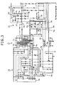
- FIG 3 is a circuit diagram of the V sus generator 52.
- the V sus generator 52 is a partial resonance circuit and the same is made up of a primary side to which a voltage rectified by the rectifier circuit 51 is directly input and a secondary side adjusted to a desired voltage through a transformer for supplying the sustain voltage V sus to the PDP.
- a control IC 70a for properly adjusting the voltage on the primary side, a resonance circuit 70b, and a primary-side feedback circuit 70c for feeding back the voltage on the secondary side 72 to the control IC 70a.
- a voltage monitor line 72g responsive to the output voltage from the secondary side for sending a signal to the primary-side feedback circuit 70c, an output line 72a from a necessary number of turns of the secondary winding 71c of the transformer 71 capable of outputting a predetermined output voltage, a detector circuit 72b dropping the voltage of the secondary side to a predetermined voltage thereby supplying the inspection voltage S - V sus to the A/D terminal of the microcomputer 60, and a detection invalidating circuit 73 supplied with 15V from outside the V sus generator 52 and enabled, based on the voltage, to supply a predetermined voltage to the A/D terminal.
- the control IC 70a is provided with a zero current detecting terminal A as a trigger input terminal to which a trigger voltage from the resonance circuit 70b is input, a GND terminal B to which a ground voltage is supplied, a feedback terminal C to which a feedback signal is input through the primary-side feedback circuit 70c, a V cc terminal D for receiving a power supply from a control winding 7 1 a, and a V in terminal F directly receiving the voltage undergoing AC rectification for supplying a current to V cc only at the time of startup and having the current automatically cut off after the startup.
- V in terminal F When a direct-current voltage DC is supplied from the rectifier circuit 51, the voltage is first applied to the V in terminal F and, thereupon, accumulation of electrical charges is started. Since the V in terminal F supplies a current at one micro ampere level to a startup circuit internal to the control IC 70a, it takes time to accumulate charges. This time constitutes a delay. Until the charges in the startup circuit reaches a predetermined amount, V cc oscillates based on the voltage input from V in and, after the charges in the startup circuit has reached the predetermined amount, V cc comes to be oscillated only by the power supply from the control wiring 71a. At the same time, the input from the Vin terminal F is automatically cut off and the supply of electrical charges from the V in terminal F is stopped.
- control IC based on a feedback signal input to the feedback terminal C, performs feedback control by PWM so that the output voltage on the secondary side may be suitably adjusted to a proper voltage and allows a collector terminal G to output a drive voltage to the main winding on the primary side of the transformer.
- the control IC further detects the zero-current point on the secondary side by inputting a voltage of the control winding of the transformer to the zero current detecting terminal A through the resonance circuit and determines the ON-timing of the main switching element for switching the output from the collector terminal G
- the primary-side feedback circuit 70c formed by having the feedback terminal C of the control IC 70a grounded through a phototransistor 70d constituting a photocoupler, is turned ON when the phototransistor 70d has received, for a predetermined period of time, light beams from a light emitting diode 70i constituting the photocoupler provided on a secondary side feedback circuit 72h, to be described later, whereby a feedback signal is input to the feedback terminal C.
- V sus output line 72a From the transformer 71 are output a V sus output line 72a outputting a voltage of approximately 175V as a sustain voltage and a voltage monitor line 72g having the secondary side feedback circuit 72h and the detector circuit 72b connected thereto.
- the V sus output line 72a is connected to the detection invalidating circuit 73 and an output line from the detection invalidating circuit 73 is connected to the detector circuit 72b to be described later.
- the secondary side feedback circuit 72h has the light-emitting diode 72i, constituting the photocoupler, connected thereto with the anode thereof directed to the monitor line 72g.
- the cathode of the light emitting diode 72i is grounded through a zener diode 72f connected oppositely to the light emitting diode 72i.
- the zener diode 72f is broken-down when the voltage of the monitor line 72g exceeds the beaking-down voltage of the zener diode 72f, whereby an electrical current flows through the light emitting diode 72i to emit light beams and the light beams are received by the phototransistor 70d.
- the detector circuit 72b includes voltage dividing resistors 72d, 72e (first dividing resistors) having first end thereof connected to the voltage monitor line 72g and second end thereof grounded and a diode 72c having its cathode connected to the voltage dividing point of the voltage dividing resistors and its anode connected to the A/D terminal of the microcomputer 60.
- the anode of the diode 72c is also connected to the output line of the detection invalidating circuit 73. More specifically, the voltage of the voltage monitor line 72g is divided by the voltage dividing resistors 72d, 72e and the voltage at the dividing point is output as the inspection voltage S - V sus .
- the A/D terminal of the microcomputer 60 detects this voltage to output "L” so that the relay circuit 55 is turned OFF and therefore the power supply circuit 50 is stopped.
- the A/D terminal of the microcomputer 60 detects this voltage and outputs "H” so that the relay circuit 55 is turned ON and therefore the power supply circuit 50 is not stopped.
- the values of the voltage dividing resistors 72d, 72e are set so that the voltage of the dividing point becomes 1.5 - 3.5V (intermediate value being 2.5V).
- the microcomputer 60 supplied with the inspection voltage S - V sus from the detector circuit 72b to thereby detect an abnormality of the V sus voltage constitutes a detecting means. Further, the microcomputer 60 outputting "L" when it determines that the voltage S - V sus is abnormal to thereby turn OFF the relay circuit constitutes a power supply switching means.
- the microcomputer 60 detects a lower voltage than a predetermined voltage through the detector circuit 72b, the microcomputer 60 stops the power supply circuit 50. Accordingly, depending on the startup timing of the microcomputer 60, the power supply circuit 50 may be stopped before the control IC 70a starts the oscillation and then the power supply circuit 50 may not start. Therefore, in the present invention, a detection invalidating circuit 73 is provided so that the power supply circuit 50 may not be stopped before the control IC 70a starts up.
- the detection invalidating circuit 73 includes a zener diode 73a, voltage dividing resistors 73b, 73c (third voltage dividing resistors), transistor 73d, voltage dividing resistors 73 e, 73f (second voltage dividing resistors), and diode 73 g; the circuit 73 is supplied with a voltage of 15V from outside the V sus generator 52.
- the zener diode 73a of which the breaking-down voltage is approximately 150V, has its cathode connected with the V sus output line and its anode connected with first end of the voltage dividing resistors 73b, 73c. Second end of the voltage dividing resistors 73b, 73c is grounded.
- the resistance values of the voltage dividing resistors 73b, 73c are so set that the voltage applied to the zener diode 73a may become approximately 150V when the output voltage of the V sus output line 72a is approximately 175V
- the voltage dividing point of the voltage dividing resistors 73b, 73c is connected with the base of the transistor 73d.
- the serially connected voltage dividing resistors 73e, 73f which are input from the outside and have a 15-volt voltage against the ground, have the voltage dividing point connected with the collector of the transistor 73d and the anode of the diode 73g.
- the voltage of 15V is supplied to the resistor 73e in the stage preceding the V sus generator 52 of the power supply circuit 50.
- the emitter of the transistor 73d is grounded.
- the cathode of the diode 73g is connected with the anode of the diode 72c of the detector circuit 72b.
- the zener diode 73a does not be broken-down and no voltage is applied to the base of the transistor 73d. Hence, the same does not turn ON. Accordingly, the externally applied voltage of 15V is reduced, through the resistor 73e and the diode 73g, to 1.5V - 3.5V (intermediate value 2.5V) and this reduced voltage is input to the A/D input port of the microcomputer 60.
- the microcomputer 60 recognizes that the sustain voltage V sus is 175V or above.
- the zener diode 73a is broken-down and turns ON the transistor 73d, whereby the externally applied voltage of 15V is pulled into the ground potential through the collector-emitter line of the transistor 73d. Therefore, a voltage based on the externally applied voltage of 15V is not supplied to the detector circuit 72b.
- the detection invalidating circuit 73 constitutes a means to invalidate detection, in which, when the V sus voltage is lower than 175V, a voltage of 1.5V - 3.5 V is output to the detector circuit 72b (i.e., to the A/D input port of the microcomputer 60) and, when the V sus voltage is 175V or above, no voltage is output to the detector circuit 72b (i.e., to the A/D input port of the microcomputer 60).
- the power supply circuit 50 is started up.
- the relay circuit 55 is turned ON and a direct-current voltage DC rectified in the rectifier circuit 51 is input to the V sus generator 52.
- outputting of the 15V line has already been started before the V sus generator 52, and the voltage of 15V is kept to be supplied to the detection invalidating circuit 73 while the V sus generator 52 is started up.
- V sus generator 52 Upon turning ON of the V sus generator 52, electrical charges are supplied to the V in terminal of the control IC 70a and electrical charges start to be stored in the startup circuit of the control IC 70a. At the same time V cc starts to oscillate by using the stored charges as the power source. Then, the V sus voltage output from the second side winding 71c of the transformer 71 gradually rises from 0V to 175V However, since the voltage of the V sus output line 72a is lower than 175V while the output of the second side winding 71c is in the course of voltage increase, the zener diode 73a does not be broken-down. Hence, the externally applied voltage of 15V is reduced to 1.5V - 3.5V by the resistor 73e and supplied to the A/D input port of the microcomputer 60.
- the voltage at the voltage dividing point S of the voltage dividing resistors 72d, 72e also starts to increase from 0V to around 2.5V (1.5V - 3.5 V).
- the voltage is lower than the voltage supplied from the detection invalidating circuit 73, it is not supplied to the A/D input port of the microcomputer 60. More specifically, since the microcomputer 60 outputs "H" as the switching signal based on the detected voltage supplied from the detection invalidating circuit 73, the switch of the relay circuit 55 continues to be kept ON.
- the zener diode 73a When the V sus voltage reaches 175V, the zener diode 73a is broken-down, and hence a current flows to the ground through the voltage dividing resistors 73b, 73c to produce a voltage at the voltage dividing point of the resistors, and this voltage is supplied to the base of the transistor 73d to turn the same ON. Then, the externally supplied voltage of 15V is pulled into the ground potential and voltage supply from the detection invalidating circuit 73 to the detector circuit 72b is stopped.
- the detection invalidating circuit 73 is configured to include: the voltage dividing resistors 73e, 73f having first end thereof supplied with a voltage from a stage preceding the sustain voltage generator 52 and second end thereof grounded; the zener diode 73 a having the cathode thereof connected with the V sus output line 72a and broken-down at a voltage around 150V; the voltage dividing resistors 73b, 73c having first end thereof connected with the anode of the zener diode 73a and second end thereof grounded; and the transistor 73d having the collector thereof connected with the voltage dividing point of the voltage dividing resistors 73e, 73f, the base thereof connected with the voltage dividing point of the voltage dividing resistors 73b, 73c, and the emitter thereof grounded, in which the voltage dividing point of the voltage dividing resistors 73e, 73f is connected with the voltage dividing point of the voltage dividing resistors 72d, 72e.
- the detection invalidating circuit 73 applies an alternative voltage to the detector circuit 72b until the voltage V sus reaches 175V and, when the voltage V sus reaches 175V or above, the same stops the supply of the alternative voltage. Accordingly, the alternative voltage indicating that the voltage V sus is 175V or above is input to the A/D input port of the microcomputer 60 even when the voltage V sus is lower than 175V and, therefore, the microcomputer 60 is prevented from outputting a switching signal at "L" to the relay circuit 55.
- the labels such as left, right, front, back, top, bottom, forward, reverse, clockwise, counter clockwise, up, down, or other similar terms such as upper, lower, aft, fore, vertical, horizontal, proximal, distal, etc. have been used for convenience purposes only and are not intended to imply any particular fixed direction or orientation. Instead, they are used to reflect relative locations and/or directions/orientations between various portions of an object.
Landscapes
- Engineering & Computer Science (AREA)
- Power Engineering (AREA)
- Physics & Mathematics (AREA)
- Plasma & Fusion (AREA)
- Computer Hardware Design (AREA)
- General Physics & Mathematics (AREA)
- Theoretical Computer Science (AREA)
- Control Of Gas Discharge Display Tubes (AREA)
- Dc-Dc Converters (AREA)
- Transforming Electric Information Into Light Information (AREA)
- Control Of Indicators Other Than Cathode Ray Tubes (AREA)
- Television Receiver Circuits (AREA)
Applications Claiming Priority (1)
| Application Number | Priority Date | Filing Date | Title |
|---|---|---|---|
| JP2006252697A JP4247640B2 (ja) | 2006-09-19 | 2006-09-19 | プラズマテレビジョンおよび電源回路 |
Publications (2)
| Publication Number | Publication Date |
|---|---|
| EP1903549A2 true EP1903549A2 (de) | 2008-03-26 |
| EP1903549A3 EP1903549A3 (de) | 2008-11-05 |
Family
ID=38846824
Family Applications (1)
| Application Number | Title | Priority Date | Filing Date |
|---|---|---|---|
| EP07015996A Withdrawn EP1903549A3 (de) | 2006-09-19 | 2007-08-14 | Plasmafernseher und Netzteilschaltung |
Country Status (4)
| Country | Link |
|---|---|
| US (1) | US20080068367A1 (de) |
| EP (1) | EP1903549A3 (de) |
| JP (1) | JP4247640B2 (de) |
| RU (1) | RU2007134737A (de) |
Cited By (1)
| Publication number | Priority date | Publication date | Assignee | Title |
|---|---|---|---|---|
| EP2306600A1 (de) * | 2009-09-30 | 2011-04-06 | Samsung Electronics Co., Ltd. | Netzteil für Fernseher und Fernseher |
Families Citing this family (1)
| Publication number | Priority date | Publication date | Assignee | Title |
|---|---|---|---|---|
| JP3113228U (ja) * | 2005-06-01 | 2005-09-02 | 船井電機株式会社 | プラズマテレビジョン |
Citations (3)
| Publication number | Priority date | Publication date | Assignee | Title |
|---|---|---|---|---|
| EP1073188A2 (de) | 1999-07-27 | 2001-01-31 | The Nippon Signal Co. Ltd. | Stromversorgungseinheit |
| US20030099122A1 (en) | 2001-11-29 | 2003-05-29 | Lg Electronics Inc. | Generator for sustaining pulse of plasma display panel |
| US20040032754A1 (en) | 2002-08-19 | 2004-02-19 | Jian Yang | Multiple output power supply having soft start protection for load over-current or short circuit conditions |
Family Cites Families (27)
| Publication number | Priority date | Publication date | Assignee | Title |
|---|---|---|---|---|
| US99122A (en) * | 1870-01-25 | warner | ||
| US32754A (en) * | 1861-07-09 | Improvement in molds for molding pipes of plastic materials | ||
| US3670246A (en) * | 1970-03-16 | 1972-06-13 | Forbro Design Corp | Under-voltage monitoring device having time delay means for regulated power supplies |
| US4685020A (en) * | 1985-05-06 | 1987-08-04 | International Business Machines Corp. | Shutdown circuit for blocking oscillator power supply |
| US5001623A (en) * | 1989-12-22 | 1991-03-19 | Burle Technologies, Inc. | Automatically switching multiple input voltage power supply |
| US5313381A (en) * | 1992-09-01 | 1994-05-17 | Power Integrations, Inc. | Three-terminal switched mode power supply integrated circuit |
| US5412308A (en) * | 1994-01-06 | 1995-05-02 | Hewlett-Packard Corporation | Dual voltage power supply |
| US5455501A (en) * | 1994-03-24 | 1995-10-03 | Intel Corporation | Multiple output DC-DC converter with different ranges of output assurance and capable of tolerating load transients |
| JP3364066B2 (ja) * | 1995-10-02 | 2003-01-08 | 富士通株式会社 | Ac型プラズマディスプレイ装置及びその駆動回路 |
| US5642018A (en) * | 1995-11-29 | 1997-06-24 | Plasmaco, Inc. | Display panel sustain circuit enabling precise control of energy recovery |
| FI970871A7 (fi) * | 1997-02-28 | 1998-08-29 | Nokia Telecommunications Oy | Hakkuriteholähde |
| US6040778A (en) * | 1998-04-20 | 2000-03-21 | France/Scott Fetzer Company | Neon power supply with midpoint ground detection and diagnostic functions |
| US6529190B2 (en) * | 1998-09-30 | 2003-03-04 | Sony Corporation | Method and apparatus for monitoring/shutting down a power line within a display device |
| JP2004528798A (ja) * | 2001-06-05 | 2004-09-16 | コーニンクレッカ フィリップス エレクトロニクス エヌ ヴィ | パワーオンおよびパワーオフ制御シーケンスをもつ電源アーキテクチャ |
| JP2003079163A (ja) * | 2001-09-04 | 2003-03-14 | Honda Motor Co Ltd | インバータ装置 |
| JP2003319649A (ja) * | 2002-02-22 | 2003-11-07 | Ricoh Co Ltd | 画像形成装置の電源回路および画像形成装置の電源制御方法 |
| JP2003280574A (ja) * | 2002-03-26 | 2003-10-02 | Fujitsu Hitachi Plasma Display Ltd | 容量性負荷駆動回路及びプラズマディスプレイ装置 |
| US7099135B2 (en) * | 2002-11-05 | 2006-08-29 | Semiconductor Components Industries, L.L.C | Integrated inrush current limiter circuit and method |
| JP2004222485A (ja) * | 2002-12-27 | 2004-08-05 | Sony Corp | スイッチング電源回路 |
| KR100601640B1 (ko) * | 2003-07-04 | 2006-07-14 | 삼성전자주식회사 | 전원회로 보호장치 |
| US7458028B2 (en) * | 2003-07-18 | 2008-11-25 | Avinash Chidambaram | Graphical interface for configuring a power supply controller |
| US7057907B2 (en) * | 2003-11-21 | 2006-06-06 | Fairchild Semiconductor Corporation | Power converter having improved control |
| KR100589314B1 (ko) * | 2003-11-26 | 2006-06-14 | 삼성에스디아이 주식회사 | 플라즈마 디스플레이 패널의 구동 방법 및 플라즈마 표시장치 |
| JP4438608B2 (ja) * | 2004-02-16 | 2010-03-24 | 株式会社デンソー | Hブリッジ回路の駆動装置及びhブリッジ回路の保護方法 |
| US7339359B2 (en) * | 2005-03-18 | 2008-03-04 | Fairchild Semiconductor Corporation | Terminal for multiple functions in a power supply |
| US7468857B2 (en) * | 2006-02-10 | 2008-12-23 | Maxtor Corporation | Acceleration feed-forward correction enabled or disabled based on track follow loop signals |
| US7310251B2 (en) * | 2006-02-24 | 2007-12-18 | System General Corp. | Control circuit having two-level under voltage lockout threshold to improve the protection of power supply |
-
2006
- 2006-09-19 JP JP2006252697A patent/JP4247640B2/ja not_active Expired - Fee Related
-
2007
- 2007-08-14 EP EP07015996A patent/EP1903549A3/de not_active Withdrawn
- 2007-09-17 US US11/901,429 patent/US20080068367A1/en not_active Abandoned
- 2007-09-18 RU RU2007134737/09A patent/RU2007134737A/ru not_active Application Discontinuation
Patent Citations (3)
| Publication number | Priority date | Publication date | Assignee | Title |
|---|---|---|---|---|
| EP1073188A2 (de) | 1999-07-27 | 2001-01-31 | The Nippon Signal Co. Ltd. | Stromversorgungseinheit |
| US20030099122A1 (en) | 2001-11-29 | 2003-05-29 | Lg Electronics Inc. | Generator for sustaining pulse of plasma display panel |
| US20040032754A1 (en) | 2002-08-19 | 2004-02-19 | Jian Yang | Multiple output power supply having soft start protection for load over-current or short circuit conditions |
Cited By (8)
| Publication number | Priority date | Publication date | Assignee | Title |
|---|---|---|---|---|
| EP2306600A1 (de) * | 2009-09-30 | 2011-04-06 | Samsung Electronics Co., Ltd. | Netzteil für Fernseher und Fernseher |
| US8860889B2 (en) | 2009-09-30 | 2014-10-14 | Samsung Electronics Co., Ltd. | Power supply for television and television including the same |
| US8917359B2 (en) | 2009-09-30 | 2014-12-23 | Samsung Electronics Co., Ltd. | Power supply for television and television including the same |
| US9179088B2 (en) | 2009-09-30 | 2015-11-03 | Samsung Electronics Co., Ltd. | Power supply for television and television including the same |
| US9407855B2 (en) | 2009-09-30 | 2016-08-02 | Samsung Electronics Co., Ltd. | Power supply for television and television including the same |
| US9693007B2 (en) | 2009-09-30 | 2017-06-27 | Samsung Electronics Co., Ltd. | Power supply for television and television including the same |
| US9955104B2 (en) | 2009-09-30 | 2018-04-24 | Samsung Electronics Co., Ltd. | Power supply for television and television including the same |
| US10321088B2 (en) | 2009-09-30 | 2019-06-11 | Samsung Electronics Co., Ltd. | Power supply for television and television including the same |
Also Published As
| Publication number | Publication date |
|---|---|
| JP4247640B2 (ja) | 2009-04-02 |
| EP1903549A3 (de) | 2008-11-05 |
| JP2008076504A (ja) | 2008-04-03 |
| US20080068367A1 (en) | 2008-03-20 |
| RU2007134737A (ru) | 2009-03-27 |
Similar Documents
| Publication | Publication Date | Title |
|---|---|---|
| KR19980014710A (ko) | 전원절약 회로를 갖는 디스플레이장치 | |
| KR100598412B1 (ko) | 디스플레이 시스템의 전원절전장치 및 전원절전방법 | |
| US8243009B2 (en) | Separately-excited inverter circuit and liquid crystal television | |
| KR101422024B1 (ko) | 평판디스플레이의 전원공급장치 | |
| US20080068367A1 (en) | Plasma television and power supply circuit | |
| US8243008B2 (en) | Separately excited inverter circuit and liquid crystal display television | |
| KR20160004093A (ko) | 디스플레이장치, 전원공급장치 및 그 전원공급방법 | |
| US6847131B2 (en) | Power supply device and electronic equipment | |
| US7446483B2 (en) | Backlight light source drive device | |
| JP3744304B2 (ja) | 電源装置 | |
| US6989639B2 (en) | Television image receiving apparatus and CRT display apparatus | |
| JP2008219646A (ja) | プラズマテレビジョン及び電源回路 | |
| KR100497236B1 (ko) | 플라즈마 디스플레이 패널의 전원 제어 장치 및 그 방법 | |
| US7936349B2 (en) | Power supply apparatus and flat-screen television set | |
| JP5413140B2 (ja) | 電源供給装置、及び画像出力装置 | |
| JP3459052B2 (ja) | 直流電源装置 | |
| JP2008107410A (ja) | フラットパネルディスプレイおよび電源回路 | |
| JP2613955B2 (ja) | 電子機器の保護装置 | |
| JP4548410B2 (ja) | プラズマディスプレイ装置 | |
| JP3278293B2 (ja) | 映像装置のx線発生防止回路 | |
| KR200319495Y1 (ko) | 영상 표시 기기의 감압 보호 장치 | |
| KR20010064562A (ko) | 피디피 티브이의 리셋 방지회로 | |
| US20080272798A1 (en) | Display device and liquid crystal television | |
| JP2002260890A (ja) | 放電灯点灯装置及びこの放電灯点灯装置を用いた画像表示装置 | |
| JPH07212679A (ja) | Crtの高圧放電回路 |
Legal Events
| Date | Code | Title | Description |
|---|---|---|---|
| PUAI | Public reference made under article 153(3) epc to a published international application that has entered the european phase |
Free format text: ORIGINAL CODE: 0009012 |
|
| AK | Designated contracting states |
Kind code of ref document: A2 Designated state(s): AT BE BG CH CY CZ DE DK EE ES FI FR GB GR HU IE IS IT LI LT LU LV MC MT NL PL PT RO SE SI SK TR |
|
| AX | Request for extension of the european patent |
Extension state: AL BA HR MK YU |
|
| PUAL | Search report despatched |
Free format text: ORIGINAL CODE: 0009013 |
|
| AK | Designated contracting states |
Kind code of ref document: A3 Designated state(s): AT BE BG CH CY CZ DE DK EE ES FI FR GB GR HU IE IS IT LI LT LU LV MC MT NL PL PT RO SE SI SK TR |
|
| AX | Request for extension of the european patent |
Extension state: AL BA HR MK RS |
|
| 17P | Request for examination filed |
Effective date: 20090310 |
|
| AKX | Designation fees paid |
Designated state(s): DE FR GB |
|
| 17Q | First examination report despatched |
Effective date: 20090714 |
|
| STAA | Information on the status of an ep patent application or granted ep patent |
Free format text: STATUS: THE APPLICATION IS DEEMED TO BE WITHDRAWN |
|
| 18D | Application deemed to be withdrawn |
Effective date: 20110329 |