EP1898293B1 - Constant current circuit - Google Patents
Constant current circuit Download PDFInfo
- Publication number
- EP1898293B1 EP1898293B1 EP07014713A EP07014713A EP1898293B1 EP 1898293 B1 EP1898293 B1 EP 1898293B1 EP 07014713 A EP07014713 A EP 07014713A EP 07014713 A EP07014713 A EP 07014713A EP 1898293 B1 EP1898293 B1 EP 1898293B1
- Authority
- EP
- European Patent Office
- Prior art keywords
- voltage
- current
- transistor
- pmos
- circuit
- Prior art date
- Legal status (The legal status is an assumption and is not a legal conclusion. Google has not performed a legal analysis and makes no representation as to the accuracy of the status listed.)
- Expired - Fee Related
Links
- 238000000034 method Methods 0.000 description 22
- 230000007423 decrease Effects 0.000 description 13
- 238000010586 diagram Methods 0.000 description 5
- 102220029016 rs1140366 Human genes 0.000 description 1
- 102220057185 rs373145667 Human genes 0.000 description 1
- 239000004065 semiconductor Substances 0.000 description 1
- 230000035945 sensitivity Effects 0.000 description 1
Images


Classifications
-
- G—PHYSICS
- G05—CONTROLLING; REGULATING
- G05F—SYSTEMS FOR REGULATING ELECTRIC OR MAGNETIC VARIABLES
- G05F3/00—Non-retroactive systems for regulating electric variables by using an uncontrolled element, or an uncontrolled combination of elements, such element or such combination having self-regulating properties
- G05F3/02—Regulating voltage or current
- G05F3/08—Regulating voltage or current wherein the variable is dc
- G05F3/10—Regulating voltage or current wherein the variable is dc using uncontrolled devices with non-linear characteristics
- G05F3/16—Regulating voltage or current wherein the variable is dc using uncontrolled devices with non-linear characteristics being semiconductor devices
- G05F3/20—Regulating voltage or current wherein the variable is dc using uncontrolled devices with non-linear characteristics being semiconductor devices using diode- transistor combinations
- G05F3/26—Current mirrors
- G05F3/262—Current mirrors using field-effect transistors only
-
- G—PHYSICS
- G05—CONTROLLING; REGULATING
- G05F—SYSTEMS FOR REGULATING ELECTRIC OR MAGNETIC VARIABLES
- G05F3/00—Non-retroactive systems for regulating electric variables by using an uncontrolled element, or an uncontrolled combination of elements, such element or such combination having self-regulating properties
- G05F3/02—Regulating voltage or current
- G05F3/08—Regulating voltage or current wherein the variable is dc
- G05F3/10—Regulating voltage or current wherein the variable is dc using uncontrolled devices with non-linear characteristics
- G05F3/16—Regulating voltage or current wherein the variable is dc using uncontrolled devices with non-linear characteristics being semiconductor devices
- G05F3/20—Regulating voltage or current wherein the variable is dc using uncontrolled devices with non-linear characteristics being semiconductor devices using diode- transistor combinations
- G05F3/26—Current mirrors
Definitions
- the present invention relates to a constant current circuit that supplies a stable output current.
- a band-gap reference circuit is known as a constant current circuit that is widely used in a semiconductor integrated circuit.
- the band-gap reference circuit is independent of power supply voltage fluctuation or process fluctuation of MOS transistors.
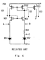
- Fig. 6 shows the technique disclosed in Koyabe.
- the technique taught by Koyabe includes P-channel MOS transistors (PMOS) P51 to P53, N-channel MOS transistors (NMOS) N51 and N52, a resistor R51, and diodes D51 and D52.
- the PMOS P51, the NMOS N51 and the diode D51 are connected in series between a power supply and a ground.
- the PMOS P52, the NMOS N52, the resistor R51 and the diode D52 are also connected in series between the power supply and the ground.
- the PMOS P51 and the PMOS P52 form a first current mirror.
- the NMOS N51 and the NMOS N52 form a second current mirror.
- the first current mirror and the second current mirror form a loop.
- the area ratio of the diode D51 and the diode D52 is 1:N.
- the NMOS N51, the NMOS N52, the PMOS P51 and the PMOS P52 have the same transistor size, and they operate in a saturation region.
- the terminal "a” is a power supply terminal
- "b” is an output terminal
- "c" is a ground terminal.
- NMOS N51 and the NMOS N52 form a current mirror, gate-source voltages Vgs of N51 and N52 are equal, so that a voltage VA at a point A and a voltage VB at a point B are equal. Therefore, a voltage drop at the resistor R51 is determined by a difference between the diodes D51 and D52.
- a current I52 is determined by a difference between the voltage VA at the point A and a voltage VC at a point C, which is VA-VC.
- Fig. 7 shows the technique disclosed in Kameyama.
- the technique taught by Kameyama uses an NMOS N53 instead of the diodes D51 and D52 used in Koyabe and further includes a feedback unit 60 having a PMOS P53, an NMOS N54 and an NMOS N55.
- the terminal "a” is a power supply terminal
- "b” is an output terminal
- "c” is a ground terminal.
- the current 152 is determined by a voltage applied to the resistor R51. If the current 152 increases, the current I53 increases accordingly.
- the voltage at the NMOS N54 is lower than the voltage at the point A, and a voltage difference between the point A and the NMOS N54 is fed back to the NMOS N53.
- the voltage at the point A decreases.
- the voltages of the point A and the point B are equal because of a current mirror, and therefore the voltage at the point B decreases as the voltage at the point A decreases. Consequently, the current 152 is suppressed, and the output current 154 is thereby also suppressed.
- Kameyama uses the feedback unit 60 to control the current fluctuation which occurs due to variations of a gate length Lg, a gate width Wg and a threshold Vt of each MOS transistor and a resistance.
- Kameyama can supply a stable output current for power supply voltage fluctuation and process fluctuation of each MOS transistor, it cannot supply a stable current for temperature fluctuation because it does not use a temperature compensating circuit or the like which uses a diode and a resistor as in Koyabe.
- US 2003/0132796 A1 discloses a constant current circuit according to the preamble of the appended claim 1.
- US 6 448 811 B1 discloses an integrated circuit current reference with reduced sensitivity to process variations.
- a constant current circuit includes a first current mirror including a first transistor formed on a first current path and a second transistor formed on a second current path, a second current mirror including a third transistor formed on the first current path and a fourth transistor formed on the second current path, a first diode formed on the first current path, a second diode formed on the second current path, a resistor formed on the second current path, a variable resistance element directly connected with the third transistor and with the resistor, and a feedback unit to control a resistance value of the variable resistance element based on a current flowing through the second current path.
- the constant current circuit includes the variable resistance element which is directly connected with the third transistor and with the resistor. It controls a resistance value of the variable resistance element according to a voltage which is fed back from the feedback unit, thereby controlling a current flowing through the second current path.
- the constant current circuit of the present invention enables supply of a stable output current with a bias circuit having a small dependence on power supply voltage fluctuation, temperature fluctuation, process fluctuation of MOS transistors and a resistor.
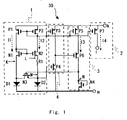
- Fig. 1 is a circuit diagram showing a constant current circuit 30 according to this embodiment.
- the constant current circuit 30 includes a band-gap reference circuit 1, a current output unit 2, an inverter circuit 3, and a first level shifter 4.
- the band-gap reference circuit 1 generates a constant output current regardless of the occurrence of power supply voltage change, process fluctuation, temperature change and so on.
- the current output unit 2 outputs a current generated in the constant current circuit of this embodiment.
- the inverter circuit 3 generates and outputs a voltage to be fed back so as to allow the output current of the band-gap reference circuit 1 to remain constant.
- the first level shifter 4 shifts a voltage at a prescribed node of the band-gap reference circuit 1 and outputs a level-shifted voltage.
- the band-gap reference circuit 1 includes PMOS transistors (PMOS) P1 and P2, NMOS transistors (NMOS) N1 to N3, a resistor R1 and diodes D1 and D2.
- the PMOS P1, the NMOS N1 and the diode D1 are connected in series between a power supply and a ground, forming a first current path.
- the PMOS P2, the NMOS N2, the resistor R1 and the diode D2 are also connected in series between the power supply and the ground, forming a second current path.
- the gates of the PMOS P1 and P2 are connected in common with the drain of the PMOS P2, so that they form a first current mirror.
- the gates of the NMOS N1 and N2 are connected in common with the drain of the NMOS N1, so that they form a second current mirror.
- the resistor R1 is placed between the NMOS N2 and the anode of the diode D2, and the NMOS N3 is connected between the anode of the diode D1 and the anode of the diode D2.
- the gate of the NMOS N3 receives an output voltage of the inverter circuit 3, which is described in detail later.
- the first level shifter 4 includes a PMOS P3 and a PMOS P4.
- the PMOS P3 and P4 are connected in series between the power supply and the ground.
- the PMOS P3 is connected with the PMOS P2 to form a current mirror.
- the gate of the PMOS P4 receives a voltage at the anode of the diode D2.
- a voltage between the PMOS P3 and the PMOS P4 is input to the inverter circuit 3.
- the inverter circuit 3 includes a PMOS P5, a PMOS P6 and an NMOS N4.
- the source of the PMOS P5 is connected with a power supply terminal, and the drain of the PMOS P5 is connected with the source of the PMOS P6.
- the gate of the PMOS P5 is connected with the drain of the PMOS P2 to form a current mirror.
- the PMOS P6 and the NMOS N4 are connected in series between the drain of the PMOS P5 and the ground voltage.
- the gate of the PMOS P6 is connected with a node between the PMOS P3 and P4.
- the current output unit 2 includes a PMOS P7 which is connected between the power supply terminal and the output terminal.
- the gate of the PMOS P7 is connected with the drain of the PMOS P2 to form a current mirror.
- the terminal “k” is a power supply terminal
- "1" is an output terminal
- “m” is a ground terminal.
- the PMOS P1 to P7 and the NMOS N1 to N4 in this embodiment have the same transistor size, and they operate in a saturation region.
- the transistors which form a current mirror in Fig. 1 may form a current mirror by cascode connection.
- the first level shifter 4 may be eliminated depending on threshold setting of transistors.
- the area ratio of the diode D1 and the diode D2 is different.
- a reference current 12 increases. If the currents flowing through the PMOS P1, P2, P5 and P7 are 11, 12, 13 and 14, respectively, I1, I2, I3, and I4 are equaled. Thus, an increase in the reference current I2 leads to an increase in the current I3 flowing through the PMOS P5.
- the increase in the current 13 causes an increase in the current flowing through the PMOS P6 and the NMOS N4. Because the PMOS P6 receives a voltage at the point M through the first level shifter 4, a gate voltage of the PMOS P6 increases.
- a voltage drop by the NMOS N4 becomes larger, and a voltage VN at the point N in the inverter circuit 3 increases.
- the inverter circuit 3 outputs the voltage VN at the point N to the gate of the NMOS N3.
- the on-resistance of the NMOS N3 decreases, thereby reducing a difference between a voltage VK at the point K and the voltage VM at the point M.
- a voltage VL at the point L decreases as the voltage VK at the point K decreases.
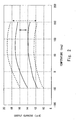
- Fig. 2 is a view to show a change in output current with respect to a change in resistance value.
- the horizontal axis indicates temperature, thus showing a change in output current with respect to temperature as well.
- the solid line and the dotted line in the upper part of the graph respectively indicate output currents when resistance values in the constant current circuit of this embodiment and the constant current circuit of the related art fall below a set value at the same rate.
- the solid line and the dotted line in the lower part of the graph respectively indicate output currents when resistance values in the constant current circuit of this embodiment and the constant current circuit of the related art exceed a set value at the same rate.
- This embodiment changes a voltage to be applied to the gate of the NMOS N3 according to a change in output current, thereby changing a voltage to be applied to the resistor R1. It is thus possible to reduce variation of an output current upon fluctuation of a resistance value as shown in Fig. 2 .
- the band-gap reference circuit 1 of the constant current circuit 30 of this embodiment includes the NMOS N3 that is a variable resistance element which is connected with the first current path composed of the PMOS P1, the NMOS N1 and the diode D1 and also connected with the second current path composed of the PMOS P2, the NMOS N2, the resistor R1 and the diode D2. Further, the constant current circuit 30 includes the inverter circuit 3 that includes the PMOS P5 which forms a current mirror together with the PMOS P2 in the second current path and feeds back an output voltage of the inverter circuit 3 to the NMOS N3.
- the present invention is not limited thereto as long as a voltage drop by a load becomes larger with an increase in current.
- the same operation as in the above embodiment is possible with the use of a resistance load as shown in Fig. 3 .
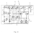
- Fig. 4 shows a constant current circuit 31, which is an alternative example for the constant current circuit 30.
- the inverter circuit 3 of the constant current circuit 30 in Fig. 1 is replaced with a differential circuit 6.
- the constant current circuit 31 shown in Fig. 4 the same elements as in the constant current circuit 30 are denoted by the same reference symbols and their detailed description is not provided herein.
- the constant current circuit 31 which is an alternative example, includes the band-gap reference circuit 1, the current output unit 2, the first level shifter 4, the differential circuit 6, and a second level shifter 5.
- the gate of the NMOS N3 receives an output voltage of the differential circuit 6, which is described in detail later.
- the gate of the PMOS P4 receives a voltage at the anode of the diode D1.
- a voltage between the PMOS P4 and the PMOS P3 is one input to the differential circuit 6.
- the gate of a PMOS P12 receives a voltage at the anode of the diode D2.
- a voltage between the PMOS P12 and a PMOS P11 is the other input to the differential circuit 6.
- the differential circuit 6 includes PMOS P8 to P10 and NMOS N5 and N6.
- the gate of the PMOS P10 is connected with the drain of the PMOS P2 to form a current mirror.
- the source of the PMOS P10 is connected with the power supply terminal, and the drain of the PMOS P10 is connected with the sources of the PMOS P8 and P9.
- the PMOS P8 and the NMOS N6 are connected in series between the drain of the PMOS P10 and the ground voltage.
- the gate of the PMOS P8 is connected with a node between the PMOS P3 and P4.
- the PMOS P9 and the NMOS N5 are connected in series between the drain of the PMOS P10 and the ground voltage.
- the gate of the PMOS P9 is connected with a node between the PMOS P11 and P12.
- the PMOS P1 to P4, the PMOS P7 to P12, the NMOS N1 to N3, N5 and N6 in this alternative example have the same transistor size, and they operate in a saturation region.
- the transistors which form a current mirror in Fig. 4 may form a current mirror by cascode connection.
- the first level shifter 4 and the second level shifter 5 may be eliminated depending on threshold setting of transistors.
- the constant current circuit 31 includes the differential circuit 6, which corresponds to the inverter circuit 3 in the constant current circuit 30, as a circuit to generate a voltage to be fed back to the gate of the NMOS N3. Specifically, the constant current circuit 31 generates a voltage VN at the point N on the basis of a difference between a voltage VK at the point K and a voltage VM at the point M using the differential circuit 6. The constant current circuit 31 operates based on a voltage difference between the point K and the point M with the use of the differential circuit 6.
- this alternative example describes the case where a voltage to be fed back to the NMOS N3 is generated in the NMOS N5
- the present invention is not limited thereto as long as a voltage drop by a load becomes larger with an increase in current.
- a current mirror load as shown in Fig. 5A or a resistance load as shown in Fig. 5B may be used instead.
- the constant current circuit 30 which includes the inverter circuit 3 generates a voltage on the basis of a voltage at the point M using the inverter circuit 3 and feeds back the generated voltage to the NMOS N3.
- the constant current circuit 31 which includes the differential circuit 6 generates a voltage on the basis of a voltage difference between the point M and the point K using the differential circuit 6 and feeds back the generated voltage to the NMOS N3.
- the feedback of the voltage corresponding to the process fluctuation in resistance of the resistor R1 to the NMOS N3 enables a decrease in variation of the current I2 which flows through the resistor R1.
Landscapes
- Engineering & Computer Science (AREA)
- Physics & Mathematics (AREA)
- Microelectronics & Electronic Packaging (AREA)
- Nonlinear Science (AREA)
- Electromagnetism (AREA)
- General Physics & Mathematics (AREA)
- Radar, Positioning & Navigation (AREA)
- Automation & Control Theory (AREA)
- Control Of Electrical Variables (AREA)
- Amplifiers (AREA)
Applications Claiming Priority (1)
| Application Number | Priority Date | Filing Date | Title |
|---|---|---|---|
| JP2006230691A JP4878243B2 (ja) | 2006-08-28 | 2006-08-28 | 定電流回路 |
Publications (2)
| Publication Number | Publication Date |
|---|---|
| EP1898293A1 EP1898293A1 (en) | 2008-03-12 |
| EP1898293B1 true EP1898293B1 (en) | 2009-03-11 |
Family
ID=38512510
Family Applications (1)
| Application Number | Title | Priority Date | Filing Date |
|---|---|---|---|
| EP07014713A Expired - Fee Related EP1898293B1 (en) | 2006-08-28 | 2007-07-26 | Constant current circuit |
Country Status (7)
| Country | Link |
|---|---|
| US (1) | US7609106B2 (zh) |
| EP (1) | EP1898293B1 (zh) |
| JP (1) | JP4878243B2 (zh) |
| KR (1) | KR20080019540A (zh) |
| CN (1) | CN101136614B (zh) |
| DE (1) | DE602007000677D1 (zh) |
| TW (1) | TW200817871A (zh) |
Families Citing this family (15)
| Publication number | Priority date | Publication date | Assignee | Title |
|---|---|---|---|---|
| US7459961B2 (en) * | 2006-10-31 | 2008-12-02 | Avago Technologies Wireless Ip (Singapore) Pte. Ltd. | Voltage supply insensitive bias circuits |
| US8008904B1 (en) * | 2008-07-31 | 2011-08-30 | Gigoptix, Inc. | Voltage and temperature invariant current setting circuit |
| JP2010109838A (ja) * | 2008-10-31 | 2010-05-13 | Nec Electronics Corp | レベルシフト回路 |
| US8183914B2 (en) * | 2009-01-12 | 2012-05-22 | Taiwan Semiconductor Manufacturing Co., Ltd. | Constant Gm circuit and methods |
| CA2717553C (en) | 2009-10-13 | 2015-06-30 | Research In Motion Limited | User interface for a touchscreen display |
| JP2011118532A (ja) * | 2009-12-01 | 2011-06-16 | Seiko Instruments Inc | 定電流回路 |
| JP5367620B2 (ja) * | 2010-03-05 | 2013-12-11 | ルネサスエレクトロニクス株式会社 | 電流源回路および半導体装置 |
| US9216257B2 (en) * | 2010-03-25 | 2015-12-22 | Medtronic, Inc. | Method and apparatus for guiding an external needle to an implantable device |
| US8475407B2 (en) | 2010-03-25 | 2013-07-02 | Medtronic, Inc. | Method and apparatus for guiding an external needle to an implantable device |
| US8483802B2 (en) | 2010-03-25 | 2013-07-09 | Medtronic, Inc. | Method and apparatus for guiding an external needle to an implantable device |
| US9339601B2 (en) | 2010-03-25 | 2016-05-17 | Medtronic, Inc. | Method and apparatus for guiding an external needle to an implantable device |
| JP5323142B2 (ja) * | 2010-07-30 | 2013-10-23 | 株式会社半導体理工学研究センター | 基準電流源回路 |
| JP5782346B2 (ja) * | 2011-09-27 | 2015-09-24 | セイコーインスツル株式会社 | 基準電圧回路 |
| KR102158801B1 (ko) | 2013-11-29 | 2020-09-23 | 삼성디스플레이 주식회사 | 발광 다이오드를 포함하는 발광 장치 및 그 구동 방법 |
| CN104615184B (zh) * | 2015-01-12 | 2016-01-13 | 华中科技大学 | 一种cmos基准电流和基准电压产生电路 |
Family Cites Families (16)
| Publication number | Priority date | Publication date | Assignee | Title |
|---|---|---|---|---|
| EP0283037B1 (en) * | 1987-03-20 | 1992-08-05 | Kabushiki Kaisha Toshiba | Controlled current producing differential circuit apparatus |
| JPH04170609A (ja) * | 1990-11-05 | 1992-06-18 | Nec Ic Microcomput Syst Ltd | 定電流回路 |
| JPH07121255A (ja) * | 1993-10-27 | 1995-05-12 | Nec Corp | 定電流源回路 |
| JP3374541B2 (ja) | 1994-08-22 | 2003-02-04 | 富士電機株式会社 | 定電流回路の温度依存性の調整方法 |
| JP2705610B2 (ja) | 1995-02-21 | 1998-01-28 | 日本電気株式会社 | 定電流源回路 |
| JP3780030B2 (ja) * | 1995-06-12 | 2006-05-31 | 株式会社ルネサステクノロジ | 発振回路およびdram |
| JP3266177B2 (ja) * | 1996-09-04 | 2002-03-18 | 住友電気工業株式会社 | 電流ミラー回路とそれを用いた基準電圧発生回路及び発光素子駆動回路 |
| US6087820A (en) * | 1999-03-09 | 2000-07-11 | Siemens Aktiengesellschaft | Current source |
| KR100400304B1 (ko) * | 2000-12-27 | 2003-10-01 | 주식회사 하이닉스반도체 | 커런트 미러형의 밴드갭 기준전압 발생장치 |
| US6448811B1 (en) * | 2001-04-02 | 2002-09-10 | Intel Corporation | Integrated circuit current reference |
| DE10139515C2 (de) * | 2001-08-10 | 2003-07-31 | Infineon Technologies Ag | Bandabstandsschaltung |
| FR2832819B1 (fr) * | 2001-11-26 | 2004-01-02 | St Microelectronics Sa | Source de courant compensee en temperature |
| US6815941B2 (en) * | 2003-02-05 | 2004-11-09 | United Memories, Inc. | Bandgap reference circuit |
| JP4632655B2 (ja) * | 2003-11-07 | 2011-02-16 | 日本電気株式会社 | 発光表示装置 |
| JP2005228160A (ja) * | 2004-02-13 | 2005-08-25 | Sony Corp | 定電流源装置 |
| US7276890B1 (en) * | 2005-07-26 | 2007-10-02 | National Semiconductor Corporation | Precision bandgap circuit using high temperature coefficient diffusion resistor in a CMOS process |
-
2006
- 2006-08-28 JP JP2006230691A patent/JP4878243B2/ja active Active
-
2007
- 2007-07-26 EP EP07014713A patent/EP1898293B1/en not_active Expired - Fee Related
- 2007-07-26 DE DE602007000677T patent/DE602007000677D1/de active Active
- 2007-08-01 KR KR1020070077376A patent/KR20080019540A/ko not_active Application Discontinuation
- 2007-08-06 TW TW096128834A patent/TW200817871A/zh unknown
- 2007-08-24 US US11/892,605 patent/US7609106B2/en not_active Expired - Fee Related
- 2007-08-28 CN CN2007101481583A patent/CN101136614B/zh not_active Expired - Fee Related
Also Published As
| Publication number | Publication date |
|---|---|
| DE602007000677D1 (de) | 2009-04-23 |
| US20080048771A1 (en) | 2008-02-28 |
| US7609106B2 (en) | 2009-10-27 |
| CN101136614B (zh) | 2012-08-15 |
| JP4878243B2 (ja) | 2012-02-15 |
| TW200817871A (en) | 2008-04-16 |
| CN101136614A (zh) | 2008-03-05 |
| EP1898293A1 (en) | 2008-03-12 |
| JP2008052639A (ja) | 2008-03-06 |
| KR20080019540A (ko) | 2008-03-04 |
Similar Documents
| Publication | Publication Date | Title |
|---|---|---|
| EP1898293B1 (en) | Constant current circuit | |
| US8446215B2 (en) | Constant voltage circuit | |
| US8384370B2 (en) | Voltage regulator with an overcurrent protection circuit | |
| US20180292854A1 (en) | Voltage regulator | |
| US7196504B2 (en) | Constant-voltage circuit, semiconductor device using the same, and constant-voltage outputting method | |
| US7990130B2 (en) | Band gap reference voltage circuit | |
| KR100393226B1 (ko) | 온도변화에 따라 내부 기준전압 값을 조절할 수 있는 내부기준전압 생성회로 및 이를 구비하는 내부 공급전압생성회로 | |
| US20080181273A1 (en) | Laser diode driving circuit | |
| WO2008144593A2 (en) | Enhanced cascode performance by reduced impact ionization | |
| US6897714B2 (en) | Reference voltage generating circuit | |
| US11025047B2 (en) | Backflow prevention circuit and power supply circuit | |
| US8441312B2 (en) | Reference current generating circuit | |
| CN110045777B (zh) | 逆流防止电路以及电源电路 | |
| US6940338B2 (en) | Semiconductor integrated circuit | |
| US8089326B2 (en) | PVT-independent current-controlled oscillator | |
| US12019462B2 (en) | Constant voltage circuit | |
| US5886571A (en) | Constant voltage regulator | |
| US7834609B2 (en) | Semiconductor device with compensation current | |
| US10873305B2 (en) | Voltage follower circuit | |
| US7474152B2 (en) | Operational amplifier circuit | |
| US10243526B1 (en) | Self-biased operational transconductance amplifier-based reference circuit | |
| JP6837894B2 (ja) | 降圧回路及び半導体集積回路 | |
| JPH05167430A (ja) | 半導体論理回路 |
Legal Events
| Date | Code | Title | Description |
|---|---|---|---|
| PUAI | Public reference made under article 153(3) epc to a published international application that has entered the european phase |
Free format text: ORIGINAL CODE: 0009012 |
|
| AK | Designated contracting states |
Kind code of ref document: A1 Designated state(s): AT BE BG CH CY CZ DE DK EE ES FI FR GB GR HU IE IS IT LI LT LU LV MC MT NL PL PT RO SE SI SK TR |
|
| AX | Request for extension of the european patent |
Extension state: AL BA HR MK YU |
|
| 17P | Request for examination filed |
Effective date: 20080606 |
|
| GRAP | Despatch of communication of intention to grant a patent |
Free format text: ORIGINAL CODE: EPIDOSNIGR1 |
|
| AKX | Designation fees paid |
Designated state(s): DE GB |
|
| GRAS | Grant fee paid |
Free format text: ORIGINAL CODE: EPIDOSNIGR3 |
|
| GRAA | (expected) grant |
Free format text: ORIGINAL CODE: 0009210 |
|
| AK | Designated contracting states |
Kind code of ref document: B1 Designated state(s): DE GB |
|
| REG | Reference to a national code |
Ref country code: GB Ref legal event code: FG4D |
|
| REF | Corresponds to: |
Ref document number: 602007000677 Country of ref document: DE Date of ref document: 20090423 Kind code of ref document: P |
|
| PLBE | No opposition filed within time limit |
Free format text: ORIGINAL CODE: 0009261 |
|
| STAA | Information on the status of an ep patent application or granted ep patent |
Free format text: STATUS: NO OPPOSITION FILED WITHIN TIME LIMIT |
|
| 26N | No opposition filed |
Effective date: 20091214 |
|
| GBPC | Gb: european patent ceased through non-payment of renewal fee |
Effective date: 20110726 |
|
| PG25 | Lapsed in a contracting state [announced via postgrant information from national office to epo] |
Ref country code: GB Free format text: LAPSE BECAUSE OF NON-PAYMENT OF DUE FEES Effective date: 20110726 |
|
| REG | Reference to a national code |
Ref country code: DE Ref legal event code: R082 Ref document number: 602007000677 Country of ref document: DE Representative=s name: GLAWE DELFS MOLL - PARTNERSCHAFT VON PATENT- U, DE |
|
| REG | Reference to a national code |
Ref country code: DE Ref legal event code: R081 Ref document number: 602007000677 Country of ref document: DE Owner name: RENESAS ELECTRONICS CORPORATION, JP Free format text: FORMER OWNER: NEC ELECTRONICS CORP., KAWASAKI, JP Effective date: 20120828 Ref country code: DE Ref legal event code: R082 Ref document number: 602007000677 Country of ref document: DE Representative=s name: GLAWE DELFS MOLL - PARTNERSCHAFT VON PATENT- U, DE Effective date: 20120828 Ref country code: DE Ref legal event code: R082 Ref document number: 602007000677 Country of ref document: DE Representative=s name: GLAWE DELFS MOLL PARTNERSCHAFT MBB VON PATENT-, DE Effective date: 20120828 Ref country code: DE Ref legal event code: R081 Ref document number: 602007000677 Country of ref document: DE Owner name: RENESAS ELECTRONICS CORPORATION, KAWASAKI-SHI, JP Free format text: FORMER OWNER: NEC ELECTRONICS CORP., KAWASAKI, KANAGAWA, JP Effective date: 20120828 |
|
| PGFP | Annual fee paid to national office [announced via postgrant information from national office to epo] |
Ref country code: DE Payment date: 20130724 Year of fee payment: 7 |
|
| REG | Reference to a national code |
Ref country code: DE Ref legal event code: R119 Ref document number: 602007000677 Country of ref document: DE |
|
| PG25 | Lapsed in a contracting state [announced via postgrant information from national office to epo] |
Ref country code: DE Free format text: LAPSE BECAUSE OF NON-PAYMENT OF DUE FEES Effective date: 20150203 |
|
| REG | Reference to a national code |
Ref country code: DE Ref legal event code: R119 Ref document number: 602007000677 Country of ref document: DE Effective date: 20150203 |