EP1892832B1 - Dünnschicht-Multimodus-Resonatorfilter mit elastischen Wellen - Google Patents
Dünnschicht-Multimodus-Resonatorfilter mit elastischen Wellen Download PDFInfo
- Publication number
- EP1892832B1 EP1892832B1 EP06766675A EP06766675A EP1892832B1 EP 1892832 B1 EP1892832 B1 EP 1892832B1 EP 06766675 A EP06766675 A EP 06766675A EP 06766675 A EP06766675 A EP 06766675A EP 1892832 B1 EP1892832 B1 EP 1892832B1
- Authority
- EP
- European Patent Office
- Prior art keywords
- balanced
- lower electrode
- vibration
- electrode
- upper electrode
- Prior art date
- Legal status (The legal status is an assumption and is not a legal conclusion. Google has not performed a legal analysis and makes no representation as to the accuracy of the status listed.)
- Not-in-force
Links
- 239000010409 thin film Substances 0.000 title claims abstract description 29
- 239000000758 substrate Substances 0.000 claims description 13
- 238000004891 communication Methods 0.000 claims description 11
- 238000006243 chemical reaction Methods 0.000 claims description 7
- 238000013016 damping Methods 0.000 description 12
- 238000010586 diagram Methods 0.000 description 12
- 230000005540 biological transmission Effects 0.000 description 11
- 230000015572 biosynthetic process Effects 0.000 description 5
- 230000008878 coupling Effects 0.000 description 5
- 238000010168 coupling process Methods 0.000 description 5
- 238000005859 coupling reaction Methods 0.000 description 5
- 238000009826 distribution Methods 0.000 description 5
- 230000000694 effects Effects 0.000 description 4
- 238000002955 isolation Methods 0.000 description 4
- 239000013078 crystal Substances 0.000 description 2
- 239000012212 insulator Substances 0.000 description 2
- 238000000034 method Methods 0.000 description 2
- 230000000644 propagated effect Effects 0.000 description 2
- PIGFYZPCRLYGLF-UHFFFAOYSA-N Aluminum nitride Chemical compound [Al]#N PIGFYZPCRLYGLF-UHFFFAOYSA-N 0.000 description 1
- ZOKXTWBITQBERF-UHFFFAOYSA-N Molybdenum Chemical compound [Mo] ZOKXTWBITQBERF-UHFFFAOYSA-N 0.000 description 1
- 230000001413 cellular effect Effects 0.000 description 1
- 230000007423 decrease Effects 0.000 description 1
- 230000003247 decreasing effect Effects 0.000 description 1
- 238000004519 manufacturing process Methods 0.000 description 1
- 239000000463 material Substances 0.000 description 1
- 229910052750 molybdenum Inorganic materials 0.000 description 1
- 239000011733 molybdenum Substances 0.000 description 1
- 230000001902 propagating effect Effects 0.000 description 1
- 239000004065 semiconductor Substances 0.000 description 1
- 238000010897 surface acoustic wave method Methods 0.000 description 1
Images


Classifications
-
- H—ELECTRICITY
- H03—ELECTRONIC CIRCUITRY
- H03H—IMPEDANCE NETWORKS, e.g. RESONANT CIRCUITS; RESONATORS
- H03H9/00—Networks comprising electromechanical or electro-acoustic devices; Electromechanical resonators
- H03H9/0023—Balance-unbalance or balance-balance networks
- H03H9/0095—Balance-unbalance or balance-balance networks using bulk acoustic wave devices
-
- H—ELECTRICITY
- H03—ELECTRONIC CIRCUITRY
- H03H—IMPEDANCE NETWORKS, e.g. RESONANT CIRCUITS; RESONATORS
- H03H9/00—Networks comprising electromechanical or electro-acoustic devices; Electromechanical resonators
- H03H9/0004—Impedance-matching networks
-
- H—ELECTRICITY
- H03—ELECTRONIC CIRCUITRY
- H03H—IMPEDANCE NETWORKS, e.g. RESONANT CIRCUITS; RESONATORS
- H03H9/00—Networks comprising electromechanical or electro-acoustic devices; Electromechanical resonators
- H03H9/02—Details
- H03H9/02007—Details of bulk acoustic wave devices
- H03H9/02062—Details relating to the vibration mode
- H03H9/0207—Details relating to the vibration mode the vibration mode being harmonic
-
- H—ELECTRICITY
- H03—ELECTRONIC CIRCUITRY
- H03H—IMPEDANCE NETWORKS, e.g. RESONANT CIRCUITS; RESONATORS
- H03H9/00—Networks comprising electromechanical or electro-acoustic devices; Electromechanical resonators
- H03H9/02—Details
- H03H9/02007—Details of bulk acoustic wave devices
- H03H9/02157—Dimensional parameters, e.g. ratio between two dimension parameters, length, width or thickness
-
- H—ELECTRICITY
- H03—ELECTRONIC CIRCUITRY
- H03H—IMPEDANCE NETWORKS, e.g. RESONANT CIRCUITS; RESONATORS
- H03H9/00—Networks comprising electromechanical or electro-acoustic devices; Electromechanical resonators
- H03H9/46—Filters
- H03H9/54—Filters comprising resonators of piezoelectric or electrostrictive material
- H03H9/56—Monolithic crystal filters
- H03H9/564—Monolithic crystal filters implemented with thin-film techniques
Definitions
- filters mounted on wireless communication devices such as cellular phones include dielectric filters, laminated filters and acoustic filters.
- Known acoustic filters include a monolithic crystal filter (MCF) using a plurality of modes of a bulk wave and a surface acoustic wave filter (SAW filter).
- MCF monolithic crystal filter
- SAW filter surface acoustic wave filter
- filters are required to have a smaller size, to provide a higher performance and to be usable at a higher frequency.
- a filmbulk acoustic resonator filter (FBAR filter) using a bulk wave of a piezoelectric thin film has been developed.
- FBAR filter a coupled FBAR filter realized by multiplexing a plurality of modes is proposed.
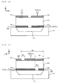
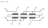
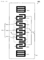
- FIG. 12 shows a structure of the conventional balanced type MCF.
- the MCF includes three electrode pairs, i.e., the electrode pair 72/76, the electrode pair 73/74, and the electrode pair 75/77.
- the electrodes of each pair face each other with a crystal substrate 71 (piezoelectric substrate) interposed therebetween.
- the electrode 72 on the left is an input electrode
- the electrode 73 on the right is an output electrode.
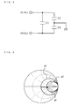
- FIG. 13 shows a structure for controlling the impedance of balanced terminals in a conventional balanced type SAW filter.
- the SAW filter has a pattern of electrodes crossing in a periodical strip-line manner on a piezoelectric substrate 601. Owing to this pattern of electrodes, an acoustic surface wave can be excited.
- a longitudinal-mode SAW filter including input IDT electrodes 602a and 602b, reflector electrodes 603a and 603b, and an output IDT electrode 604 is provided.
- the output IDT electrode 604 is divided into three, i.e., first, second and third divided IDT electrodes 604a, 604b and 604c.
- the output IDT electrode 604 is formed of a group of the three IDT electrodes 604a, 604b and 604c connected to each other.
- the first through third divided IDT electrodes 604a, 604b and 604c are located to have the same phase.
- FIG. 14 shows a capacitance equivalent circuit diagram between the output balanced terminals of the balanced type SAW filter shown in FIG. 13 .
- Capacitances Ca through Cc are respectively capacitances of the first through third divided IDT electrodes 604a through 604c, and a synthesized capacitance of the capacitances Ca through Cc is a total capacitance Cout of the output IDT electrode 604.
- the logarithmof the electrode fingers included in the output IDT electrode 604 the value of the total capacitance Cout can be controlled.
- the impedance between the output balanced terminals can be controlled by varying the logarithm of the first through third divided IDT electrodes 604a through 604c.
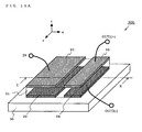
- FIG. 15A is an isometric view showing a structure of a conventional balanced/unbalanced type coupled FBAR filter 900.
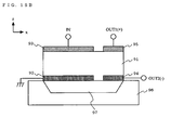
- FIG. 15B is a cross-sectional view of the conventional balanced/unbalanced type coupled FBAR filter 900 shown in FIG. 15A taken along line E-E.
- the conventional balanced/unbalanced type coupled FBAR filter 900 includes first and second lower electrodes 92 and 94, a piezoelectric thin film 91, and first and second upper 6 electrodes 93 and 95, which are provided on a substrate 96.
- the first lower electrode 92, the first upper electrode 93, and the piezoelectric thin film 91 interposed between these electrodes form a first vibration section.
- the first upper electrode 93 is used as an input terminal
- the first lower electrode 92 is used as a GND terminal.
- the second lower electrode 94, the second upper electrode 95, and the piezoelectric thin film 91 interposed between these electrodes form a second vibration section.
- the second upper electrode 95 is used as an output balanced terminal (+), and the second lower electrode 94 is used as an output balanced terminal (-).
- the substrate 96 has a cavity 97 formed therein, which is capable of commonly guaranteeing vibrations of the first and second vibration sections and coupling the vibrations. Owing to this, for example, the second vibration section on the output side excites a mechanical vibration by the mechanical vibration excited in the first vibration section on the input side, and second vibration section on the output side further converts the excited mechanical vibration into an electric signal and outputs the electric signal.
- the vibration excited in a thickness direction in the second vibration section on the output side is at ⁇ /2.
- the resonant frequency in the second vibration section is fr and the average sonic speed in the thickness direction is V
- the wavelength ⁇ is represented by V/fr. Accordingly, in the case where the second vibration section is designed to have such a thickness as to obtain the resonant frequency fr, an electric signal which is output from a top surface of the piezoelectric thin film 91 and an electric signal which is output from a bottom surface of the piezoelectric thin film 91 at the resonant frequency fr would ideally have a phase difference of 180 degrees and an amplitude difference of 180 degrees. Therefore, a single phase electric signal which is input to an input terminal IN1 is converted into differential electric signals by the balanced/unbalanced type coupled FBAR filter 900 and is output from output terminals OUT1 (+) and OUT2(-).
- FIG. 16A is an isometric view showing a structure of another conventional balanced/unbalanced type coupled FBAR filter 800.
- FIG. 16B is a cross-sectional view of the conventional balanced/unbalanced type coupled FBAR filter 800 shown in FIG. 16A taken along line F-F.
- the elements of FBAR filter 800 denoted by 8x reference signs correspond to the respective elements of FBAR filter 900 denoted by 9x reference signs.
- the structure of the balanced/unbalanced type coupled FBAR filter 800 is different from that of the balanced/unbalanced type coupled FBAR filter 900 only in the shape of the second upper electrode and the second lower electrode. The principle of controlling the impedance is the same and will not be repeated here.
- Patent Documents 3 and 4 show general state of the relevant art.
- Patent Document 3 discloses a component, having coupled resonators, which offers improved transmission characteristics of bulk acousticwaves.
- Patent Document 4 discloses a double-mode piezoelectric filter which improves attenuation on the side of lower frequencies that the center frequency.
- Patent Document 1 Japanese Laid-Open Patent Publication No. 2001-53580
- Patent Document 2 Japanese Laid-Open Patent Publication No. 2003-92526
- Patent Document 3 US 2005/012570 A1
- Patent Document 4 Japanese Laid-Open Patent Publication No. 2001-326556
- FIG. 17 shows ideal vibration mode distributions of the conventional balanced/unbalanced type coupled FBAR filter 900 shown in FIG. 15A and FIG. 15B .
- An integral value of the vibration mode distribution curves is generally equivalent to the amount of charge generated in the piezoelectric thin film 9].
- the area size of the second lower electrode 94 and the second upper electrode 95 is smaller than the area size of the first lower electrode 92 and the first upper electrode 93. Therefore, the amount of charge generated in the second vibration section is smaller. For this reason, the charge generated in the first vibration section cannot be efficiently used in the second vibration section, which increases the loss and narrows the resonant frequency band.
- the balanced/unbalanced type coupled FBAR filter 900 can significantly convert the impedance, but has a problem that the loss is increased and the resonant frequency band is narrowed.
- FIG. 18 shows ideal vibration mode distributions of the conventional balanced/unbalanced type coupled FBAR filter 800 shown in FIG. 16A and FIG. 16B .
- the balanced/unbalanced type coupled FBAR filter 800 there is a discontinuous surface between the first vibration section and the second vibration section with respect to the vibration propagating in the x direction. On the discontinuous surface, an unnecessary mode is generated.
- the ratio in an area above the cavity occupied by a non-electrode portion is higher than that in the conventional balanced/unbalanced type coupled FBAR filter 900.
- the electrode area size of the second vibration section is smaller than the electrode area size of the first vibration section. Therefore, the charge generated in the first vibration section cannot be efficiently used in the second vibration section.
- the balanced/unbalanced type coupled FBAR filter 800 can significantly convert the impedance, but has a problem that the loss is increased, the unnecessary mode is generated, and the resonant frequency band is narrowed.
- an object of the present invention is to provide a balanced/unbalanced type coupled FBAR filter efficiently using the generated charge in input/output vibration sections, having superb characteristics and controlling the impedance.
- a coupled FBAR filter according to the present invention comprises a First vibration section including an FBAR; a second vibration section including an FBAR and located parallel to the first vibration section; and a common vibration guaranteeing section, having the first and second vibration sections provided thereon, for commonly guaranteeing a vibration of the first vibration section and a vibration of the second vibration section so as to couple the two vibrations.
- the second lower electrode and the second upper electrode are both used as an input/output terminal.
- An area size of the first Lower electrode is generally equal to a total area size of the second and third lower electrodes and the area for isolating the second and third lower electrodes;
- an area size of the first upper electrode is generally equal to a total area size of the second and third upper electrodes and the area for isolating the second and third upper electrodes; and a part of the second lower electrode and a part of the second upper electrode are located to face each other.
- an area size of the third lower electrode is generally equal to an area size of the third upper electrode; and thus the third lower electrode and the third upper electrode are located to be rotation-symmetrical with respect to a central axis in a width direction of the second vibration section, that width direction being the direction from the first to the second vibration section.
- the common vibration guaranteeing section is a cavity formed in a substrate, or an acoustic mirror layer including a high acoustic impedance layer and a low acoustic impedance layer located alternately.
- the present invention may be provided as a ladder-type filter, a duplexer, or a communication device including the above-described coupled FBAR filter.
- the total area of the electrodes forming the first vibration section is generally equal to the total area of the electrodes forming the second vibration section. Therefore, the loss of the vibration propagated from the vibration section on the input side to the vibration section on the output side can be prevented, and thus the resonant frequency band can be widened. Since the first vibration section and the second vibration section face each other, generation of an unnecessary mode can be prevented.
- the impedance can be adjusted between the input side and the output side by adjusting the area size of the parts of the second lower electrode and the second upper electrode which face each other. By providing a rotation-symmetrical arrangement, the balancing performance can be improved.
- FIG. 1A is an isometric view showing a structure of a balanced/unbalanced type coupled FBAR filter 100 according to a first embodiment of the present invention.
- FIG. 1A is an isometric view showing a structure of a balanced/unbalanced type coupled FBAR filter 100 according to a first embodiment of the present invention.
- FIG. 1B is a cross-sectional view of the balanced/unbalanced type coupled FBAR filter 100 shown in FIG. 1A taken along line A-A.
- FIG. 1C is a cross-sectional view of the balanced/unbalanced type coupled FBAR filter 100 shown in FIG. 1A taken along line B-B. As shown in FIG. 1A through FIG.
- the balanced/unbalanced type coupled FBAR filter 100 includes a substrate 110, a cavity 111, a piezoelectric thin film 101, a first lower electrode 102, a second lower electrode 104, a third lower electrode 106, a first upper electrode 103, a second upper electrode 105, and a third upper electrode 107.
- the directions represented by x, y and z axes in FIG. 1A through FIG. 1C correspond to the directions specified below.
- the piezoelectric thin film 101 is shown as being transparent for easier understanding of the structure.
- the first lower electrode 102, the first upper electrode 103 , and a part of the piezoelectric thin film 101 interposedbetween these upper and lower electrodes form a first vibration section.
- the second and third upper electrodes 105 and 107, the second and third lower electrodes 104 and 106, and a part of the piezoelectric thin film 101 interposed between these upper and lower electrodes form a second vibration section.
- the first vibration section and the second vibration section are located parallel to each other on the substrate 110 while being separated from each other in the x direction.
- the substrate 110 has the cavity 111 for confining the vibration.
- the second lower electrode 104 and the third lower electrode 106 are separated from each other in the y direction by an insulating area, and the second upper electrode 105 and the third upper electrode 107 are separated from each other in the y direction by an insulating area.
- the first lower electrode 102 and the first upper electrode 103 are formed to have generally the same length (y direction) and width (x direction), i.e., generally the same area size.
- the second lower electrode 104 and the second upper electrode 105 are formed to have generally the same length and width, i.e., generally the same area size.
- the third lower electrode 106 and the third upper electrode 107 are formed to have generally the same length and width, i.e. , generally the same area size.
- the second lower electrode 104 and the third lower electrode 106 are located on the same plane while being separated from each other in the y direction by the insulating area having a width W3.
- the second upper electrode 105 and the third upper electrode 107 are located on the same plane while being separated from each other in the y direction by the insulating area having a width W4.
- the second lower electrode 104 and the second upper electrode 105 are offset in the y direction by a width W1.
- the third lower electrode 106 and the third upper electrode 107 are offset in the y direction by a width W2.
- a total area size of the second lower electrode 104, the third lower electrode 106 and the insulating area having the width w3 is generally equal to the area size of the first lower electrode 102.
- a total area size of the second upper electrode 105, the third upper electrode 107 and the insulating area having the width W4 is generally equal to the area size of the first upper electrode 103.
- the second and third lower and upper electrodes 104 through 107 are located so as to be rotation-symmetrical with respect to the central axis of the second vibration section extending in the x direction, the balancing performance is improved.
- the structure of the balanced/unbalanced type coupled FBAR filter 100 has the following three features.
- either the first vibration section or the second vibration section which is on the input side excites a mechanical vibration from an input electric signal and propagates the mechanical vibration to the vibration section on the output side.
- the vibration section on the output side converts the excited mechanical vibration into an electric signal and outputs the electric signal.
- the impedance can be controlled.
- the cavity 111 commonly guarantees the vibrations of the first and second vibration sections and thus acts as a common vibration coupling section for coupling the vibrations.
- the first upper electrode 103 is used as an input terminal IN and the first lower electrode 102 is used as a grounding terminal GND.
- the input terminal IN and the grounding terminal GND may be exchanged with each other
- the third lower electrode 106 and the third upper electrode 107 are grounded.
- an unbalanced signal (single phase signal) is input to the first upper electrode 103, and thus a voltage is applied between the first upper electrode 103 and the first lower electrode 102. Then, a vibration is excited to generate a plurality of modes resonating at a plurality of resonant frequencies in a transverse direction (x direction). At this point, it is preferable that the first vibration section couples a first-order mode and a second-order mode. Thus, a wide-band filter characteristic can be realized.
- differential electric signals are output: from a terminal OUT1 (+) connected to the second upper electrode 105 and a terminal OUT2 (-) connected to the second lower electrode 104.
- FIG. 2 is a simplified equivalent circuit diagram of the second vibration section.
- C1 is a damping capacitance formed by the second lower electrode 104 and the second upper electrode 105 facing each other
- C2 is a damping capacitance formed by the second lower electrode 104 and the third upper electrode 107 facing each other
- C3 is a damping capacitance formed by the second upper electrode 105 and the third lower electrode 106 facing each other.
- the damping capacitance C1 is connected in series between the two output balanced terminals OUT1 (+) (the second upper electrode 105) and OUT2 (-) (the second lower electrode 104).
- a series circuit of the damping capacitances C2 and C3 is connected parallel to the damping capacitance C1.
- a connection point between the damping capacitances C2 and C3 is grounded.
- a total capacitance Cout seen from the output balanced terminals OUT1 (+) and OUT2 (-) is obtained by (C1 ⁇ ⁇ C2 + C2 ⁇ C3 + C3 ⁇ C1) / (C2 + C3).
- the impedance seen from the output balanced terminals OUT1 (+) and OUT2 (-) is in inverse proportion to the total capacitance Cout.
- the damping capacitances C1 through C3 are each in proportion to the area size of the parts cf the corresponding electrodes which face each other.
- the impedance can be adjusted by adjusting the ratio among three area sizes, i.e., an area size of the parts of the second lower electrode 104 and the second upper electrode 105 which face each other, an area size of the parts of the second lower electrode 104 and the third upper electrode 107 which face each other, and an area size of the parts of the second upper electrode 105 and the third lower electrode 106 which face each other.
- a damping capacitance between the first lower electrode 102 and the first upper electrode 103 is C0.
- the total capacitance Cout of the second vibration section is equal to the damping capacitance C0.
- the third upper electrode 107, the third lower electrode 106 and the second upper electrode 105 each have an area size which is half of that of the first vibration section, the total capacitance Cout is 1/4 ⁇ C0.
- the impedance can be adjusted in the range of zin ⁇ z ⁇ 4zin, where Zin is the impedance of the vibration section on the input side which is calculated based on the damping capacitance C0 between the first lower electrode 102 and the first upper electrode 103 on the input side.
- FIG. 3 is a Smith chart illustrating an exemplary change in the impedance when the area size ratio between the upper electrode and the lower electrode in the vibration section on the output side is changed.
- a1 is the impedance when neither the third lower electrode 106 nor the third upper electrode 107 exists and thus the second lower electrode 104 and the second upper electrode 105 entirety face each other.
- a2 is the impedance when 1/3 of the second lower electrode 104 in the length direction and 1/3 of the second upper electrode 105 in the length direction face each other.
- a3 is the impedance when 1/5 of the second lower electrode 104 in the length direction and 1/5 of the second upper electrode 105 in the length direction face each other. As shown in FIG.
- the balanced/unbalanced type coupled FBAR, filter 100 makes the total area size of the electrodes forming the first vibration section generally equal to the total area size of the electrodes forming the second vibration section. Owing to this, the loss of the vibration propagated between the vibration sections is prevented, and thus the charge generated in the vibration section on the input side can be efficiently used in the vibration section on the output side. As a result, the resonant frequency band can be widened. Since the first vibration section and the second vibration section have generally the same shape and are located to face each other, generation of an unnecessary mode is prevented.
- the balanced/unbalanced type coupled FBAR filter 100 having one input terminal and two output terminals is described.
- a balanced/balanced type coupled FBAR filter 110 may be provided by adding one more input terminal to the above-described structure.
- the electrodes in the first vibration section of the balanced/balanced type coupled FBAR filter 110 may be divided to obtain a balanced/balanced type coupled FBAR, filter 120 shown in FIG. 5A and FIG. 5B .
- the impedance on the input side can further be converted.
- the cavity 111 may be replaced with an acoustic mirror layer 112 including low acoustic impedance layers and high acoustic impedance layers located alternately. Substantially the same effects are provided.
- FIG. 7A is a cross-sectional view showing a structure of a balanced/unbalanced type coupled FBAR filter 200 according to a second embodiment of the present invention.
- the crows-sectional view shown in FIG. 7A corresponds to the cross-sectional view shown in FIG. 1B taken along line A-A.
- the balanced/unbalanced type coupled FBAR, filter 200 has the following features in addition to those of the balanced/unbalanced type coupled FBAR filters 100 according to the first embodiment.
- a condition for realizing the features 1 through 3 is to provide a second insulator 108 having a greater thickness than that of the first lower electrode 102 below the second and third lower electrodes 104 and 106.
- the amount of the piezoelectric thin film 101 stacked is managed by time. Therefore, the piezoelectric thin film 101 stacked on the first lower electrode 102 and the piezoelectric thin film 101 stacked on the second and third lower electrodes 104 and 106 have an equal thickness.
- the difference in level between a top surface of the second and third lower electrodes 104 and 106 and a top surface of the first lower electrode 102 usually appears as a surface step of the piezoelectric thin film 101.
- Another condition for realizing the features 1 through 3 is to make the thickness of the first upper electrode 103 smaller than the height of the surface step of the piezoelectric thin film 101.
- a first insulator 109 is stacked on the first vibration section (on the first upper electrode 103) to a level matching the level of the second and third upper electrodes 105 and 107.
- the balanced/unbalanced type coupled FBAR filter 200 can prevent the generated charge from being consumed in a non-electrode portion, unlike the structure of the first embodiment. Owing to this, the vibration modes of the two vibration sections can be efficiently coupled. Therefore, the generated charge can be efficiently used, and smaller-loss and wider-band characteristics can be realized.
- a balanced/balanced type coupled FBAR filter 21C may be provided by adding one more input terminal to the balanced/unbalanced type coupled FBAR filter 200 according to the second embodiment.
- the balanced/unbalanced type coupled FBAR filter 401 is connected between the transmission circuit 405 and the switching circuit 403, and has a characteristic of passing through a transmission frequency band. The sizes of the electrodes therein are adjusted to match the impedance between the circuits.
- the balanced/unbalanced type coupled FBAR filter 401 converts a balanced signal from the transmission circuit 405 into an unbalanced signal and inputs the unbalanced signal to the switching circuit 403.
- the balanced/unbalanced type coupled FBAR filter 402 is connected between the receiving circuit 406 and the switching circuit 403, and has a characteristic of passing through a receiving frequency band. The sizes of the electrodes therein are adjusted to match the impedance between the circuits.
- the balanced/unbalanced type coupled FBAR filter 501 allows only a signal of a transmission frequency band to pass therethrough, matches the impedance between the antenna 504 and the transmission circuit, and converts a balanced signal from the transmission circuit into an unbalanced signal and outputs the unbalanced signal from the antenna 504.
- the balanced/unbalanced type coupled FBAR filter 502 allows only a signal of a receiving frequency band to pass Wherethrough, matches the impedance between the isolation phase shifter 503 and the receiving circuit, and converts an unbalanced signal from the isolation phase shifter 503 into a balanced signal and inputs the balanced signal to the receiving circuit.
- a duplexer which has a smaller loss and is usable over a wider band can be realized.
Landscapes
- Physics & Mathematics (AREA)
- Acoustics & Sound (AREA)
- Chemical & Material Sciences (AREA)
- Crystallography & Structural Chemistry (AREA)
- Piezo-Electric Or Mechanical Vibrators, Or Delay Or Filter Circuits (AREA)
Claims (11)
- Gekoppelter FBAR-Filter (100) symmetrischer/unsymmetrischer Art zum Durchführen einer Umwandlung zwischen einem symmetrischen Signal und einem unsymmetrischen Signal unter der Verwendung von FBARs, wobei der gekoppelte FBAR-Filter symmetrischer/unsymmetrischer Art umfasst:einen ersten Schwingungsabschnitt, welcher einen FBAR enthält;einen zweiten Schwingungsabschnitt, welcher einen FBAR enthält und parallel zum ersten Schwingungsabschnitt positioniert ist; undeinen gemeinsamen schwingungsgarantierenden Abschnitt (111, 112), auf welchem der erste und der zweite Schwingungsabschnitt vorgesehen sind, zum gemeinsamen Garantieren einer Schwingung des ersten Schwingungsabschnitts und einer Schwingung des zweiten Schwingungsabschnitts, um die beiden Schwingungen zu koppeln;wobei:der erste Schwingungsabschnitt enthält:eine erste untere Elektrode (102);eine erste obere Elektrode (103), welche gegenüber der ersten unteren Elektrode (102) positioniert ist; undeinen Teil eines piezoelektrischen dünnen Films (101), welcher zwischen der ersten unteren Elektrode (102) und der ersten oberen Elektrode (103) zwischengeschaltet ist;wobei entweder die erste untere Elektrode (102) oder die erste obere Elektrode (103) als ein Eingabe-/Ausgabeanschluss verwendet wird;der zweite Schwingungsabschnitt enthält:eine zweite untere Elektrode (104);eine dritte untere Elektrode (106), welche von der zweiten unteren Elektrode (104) durch einen isolierenden Bereich getrennt ist;eine zweite obere Elektrode (105), welche gegenüber einem Teil der dritten unteren Elektrode (106) positioniert ist;eine dritte obere Elektrode (107), welche gegenüber einem Teil der zweiten unteren Elektrode (104) positioniert ist und von der zweiten oberen Elektrode (105) durch einen isolierenden Bereich getrennt ist; undeinen weiteren Teil des piezoelektrischen dünnen Films (101), welcher zwischen der zweiten und dritten unteren Elektrode (104, 106) und der zweiten und dritten oberen Elektrode (105, 107) zwischengeschaltet ist;wobei die zweite untere Elektrode (104) und die zweite obere Elektrode (105) beide als ein Eingabe-/Ausgabeanschluss verwendet werden;eine Bereichsgröße der ersten unteren Elektrode (102) im Allgemeinen gleich einer Gesamtbereichsgröße der zweiten und dritten unteren Elektrode (104, 106) und dem Bereich zum Isolieren der zweiten und dritten unteren Elektrode (104, 106) ist;eine Bereichsgröße der ersten oberen Elektrode (103) im Allgemeinen gleich einer Gesamtbereichsgröße der zweiten und dritten oberen Elektrode (105, 107) und dem Bereich zum Isolieren der zweiten und dritten oberen Elektrode (105, 107) ist; undein Teil der zweiten unteren Elektrode (104) und ein Teil der zweiten oberen Elektrode (105) einander gegenüber positioniert sind.
- Gekoppelter FBAR-Filter symmetrischer/unsymmetrischer Art nach Anspruch 1, wobei:eine Bereichsgröße der dritten unteren Elektrode (106) im Allgemeinen gleich einer Bereichsgröße der dritten oberen Elektrode (107) ist; unddie dritte untere Elektrode (106) und die dritte obere Elektrode (107) rotationssymmetrisch bezüglich einer Mittelachse in einer Breitenrichtung des zweiten Schwingungsabschnitts positioniert sind, wobei die Breitenrichtung die Richtung vom ersten zum zweiten Schwingungsabschnitt ist.
- Gekoppelter FBAR-Filter symmetrischer/unsymmetrischer Art nach Anspruch 1, wobei:der gemeinsame schwingungsgarantierende Abschnitt eine in einem Substrat (110) gebildete Kavität (111) ist.
- Gekoppelter FBAR-Filter symmetrischer/unsymmetrischer Art nach Anspruch 1, wobei:der gemeinsame schwingungsgarantierende Abschnitt eine akustische Spiegelschicht (112) ist, welche eine Schicht hoher akustischer Impedanz und eine alternativ positionierte Schicht niedriger akustischer Impedanz enthält.
- Gekoppelter FBAR-Filter (110) symmetrischer/symmetrischer Art zum Durchführen einer Umwandlung zwischen einem symmetrischen Signal und einem symmetrischen Signal unter Verwendung von FBARs, wobei der gekoppelte FBAR-Filter symmetrischer/symmetrischer Art umfasst:einen ersten Schwingungsabschnitt, welcher einen FBAR enthält;einen zweiten Schwingungsabschnitt, welcher einen FBAR enthält und parallel zum ersten Schwingungsabschnitt positioniert ist; undeinen gemeinsamen schwingungsgarantierenden Abschnitt (111, 112), auf welchem der erste und der zweite Schwingungsabschnitt vorgesehen sind, zum gemeinsamen Garantieren einer Schwingung des ersten Schwingungsabschnitts und einer Schwingung des zweiten Schwingungsabschnitts, um die beiden Schwingungen zu koppeln;wobei:der erste Schwingungsabschnitt enthält:eine erste untere Elektrode (102);eine erste obere Elektrode (103), welche gegenüber der ersten unteren Elektrode (102) positioniert ist; undeinen Teil eines piezoelektrischen dünnen Films (101), welcher zwischen der ersten unteren Elektrode (102) und der ersten oberen Elektrode (103) zwischengeschaltet ist;wobei die erste untere Elektrode (102) und die erste obere Elektrode (103) beide als ein Eingabe-/Ausgabeanschluss verwendet werden;der zweite Schwingungsabschnitt enthält:eine zweite untere Elektrode (104);eine dritte untere Elektrode (106), welche von der zweiten unteren Elektrode (104) durch einen isolierenden Bereich getrennt ist;eine zweite obere Elektrode (105), welche gegenüber einem Teil der dritten unteren Elektrode (106) positioniert ist;eine dritte obere Elektrode (107), welche gegenüber einem Teil der zweiten unteren Elektrode (104) positioniert ist und von der zweiten oberen Elektrode (105) durch einen isolierenden Bereich getrennt ist; undeinen weiteren Teil des piezoelektrischen dünnen Films (101), welcher zwischen der zweiten und dritten unteren Elektrode (104, 106) und der zweiten und dritten oberen Elektrode (105, 107) zwischengeschaltet ist;wobei die zweite untere Elektrode (104) und die zweite obere Elektrode (105) beide als ein Eingabe-/Ausgabeanschluss verwendet werden;eine Bereichsgröße der ersten unteren Elektrode (102) im Allgemeinen gleich einer Gesamtbereichsgröße der zweiten und dritten unteren Elektrode (104, 106) und dem Bereich zum Isolieren der zweiten und dritten unteren Elektrode (104, 106) ist;eine Bereichsgröße der ersten oberen Elektrode (103) im Allgemeinen gleich einer Gesamtbereichsgröße der zweiten und dritten oberen Elektrode (105, 107) und dem Gebiet zum Isolieren der zweiten und dritten oberen Elektrode (105, 107) ist; undein Teil der zweiten unteren Elektrode (104) und ein Teil der zweiten oberen Elektrode (105) einander gegenüber positioniert sind.
- Gekoppelter FBAR-Filter symmetrischer/symmetrischer Art nach Anspruch 5, wobei:eine Bereichsgröße der dritten unteren Elektrode (106) im Allgemeinen gleich einer Bereichsgröße der dritten oberen Elektrode (107) ist; unddie dritte untere Elektrode (106) und die dritte obere Elektrode (107) rotationssymmetrisch bezüglich einer Mittelachse in einer Breitenrichtung des zweiten Schwingungsabschnitts positioniert sind, wobei die Breitenrichtung die Richtung vom ersten zum zweiten Schwingungsabschnitt ist.
- Gekoppelter FBAR-Filter symmetrischer/symmetrischer Art nach Anspruch 5, wobei:der gemeinsame schwingungsgarantierende Abschnitt eine in einem Substrat (110) gebildete Kavität (111) ist.
- Gekoppelter FBAR-Filter symmetrischer/symmetrischer Art nach Anspruch 5, wobei:der gemeinsame schwingungsgarantierende Abschnitt eine akustische Spiegelschicht (112) ist, welche eine Schicht hoher akustischer Impedanz und eine alternativ positionierte Schicht niedriger akustischer Impedanz enthält.
- Abzweigfilter (300) enthaltend den gekoppelten FBAR-Filter (303) nach Anspruch 1 oder Anspruch 5.
- Duplexer (500) enthaltend den FBAR-Filter (501, 502) nach Anspruch 1 oder Anspruch 5.
- Kommunikationsvorrichtung (400) enthaltend den gekoppelten FBAR-Filter (401, 402) nach Anspruch 1 oder Anspruch 5.
Applications Claiming Priority (2)
| Application Number | Priority Date | Filing Date | Title |
|---|---|---|---|
| JP2005177729 | 2005-06-17 | ||
| PCT/JP2006/311906 WO2006134959A1 (ja) | 2005-06-17 | 2006-06-14 | 多重モード薄膜弾性波共振器フィルタ |
Publications (4)
| Publication Number | Publication Date |
|---|---|
| EP1892832A1 EP1892832A1 (de) | 2008-02-27 |
| EP1892832A8 EP1892832A8 (de) | 2008-04-16 |
| EP1892832A4 EP1892832A4 (de) | 2009-09-16 |
| EP1892832B1 true EP1892832B1 (de) | 2011-09-21 |
Family
ID=37532314
Family Applications (1)
| Application Number | Title | Priority Date | Filing Date |
|---|---|---|---|
| EP06766675A Not-in-force EP1892832B1 (de) | 2005-06-17 | 2006-06-14 | Dünnschicht-Multimodus-Resonatorfilter mit elastischen Wellen |
Country Status (5)
| Country | Link |
|---|---|
| US (1) | US7414495B2 (de) |
| EP (1) | EP1892832B1 (de) |
| JP (1) | JPWO2006134959A1 (de) |
| CN (1) | CN100566154C (de) |
| WO (1) | WO2006134959A1 (de) |
Families Citing this family (54)
| Publication number | Priority date | Publication date | Assignee | Title |
|---|---|---|---|---|
| US7275292B2 (en) * | 2003-03-07 | 2007-10-02 | Avago Technologies Wireless Ip (Singapore) Pte. Ltd. | Method for fabricating an acoustical resonator on a substrate |
| US7531943B2 (en) * | 2004-03-31 | 2009-05-12 | Panasonic Corporation | Acoustic resonator and filter |
| US7388454B2 (en) | 2004-10-01 | 2008-06-17 | Avago Technologies Wireless Ip Pte Ltd | Acoustic resonator performance enhancement using alternating frame structure |
| US8981876B2 (en) | 2004-11-15 | 2015-03-17 | Avago Technologies General Ip (Singapore) Pte. Ltd. | Piezoelectric resonator structures and electrical filters having frame elements |
| US7202560B2 (en) | 2004-12-15 | 2007-04-10 | Avago Technologies Wireless Ip (Singapore) Pte. Ltd. | Wafer bonding of micro-electro mechanical systems to active circuitry |
| US7791434B2 (en) | 2004-12-22 | 2010-09-07 | Avago Technologies Wireless Ip (Singapore) Pte. Ltd. | Acoustic resonator performance enhancement using selective metal etch and having a trench in the piezoelectric |
| US7369013B2 (en) | 2005-04-06 | 2008-05-06 | Avago Technologies Wireless Ip Pte Ltd | Acoustic resonator performance enhancement using filled recessed region |
| WO2006112260A1 (ja) * | 2005-04-13 | 2006-10-26 | Murata Manufacturing Co., Ltd. | 圧電薄膜フィルタ |
| US7737807B2 (en) * | 2005-10-18 | 2010-06-15 | Avago Technologies Wireless Ip (Singapore) Pte. Ltd. | Acoustic galvanic isolator incorporating series-connected decoupled stacked bulk acoustic resonators |
| US7675390B2 (en) | 2005-10-18 | 2010-03-09 | Avago Technologies Wireless Ip (Singapore) Pte. Ltd. | Acoustic galvanic isolator incorporating single decoupled stacked bulk acoustic resonator |
| US20070210748A1 (en) * | 2006-03-09 | 2007-09-13 | Mark Unkrich | Power supply and electronic device having integrated power supply |
| US7746677B2 (en) | 2006-03-09 | 2010-06-29 | Avago Technologies Wireless Ip (Singapore) Pte. Ltd. | AC-DC converter circuit and power supply |
| US7479685B2 (en) | 2006-03-10 | 2009-01-20 | Avago Technologies General Ip (Singapore) Pte. Ltd. | Electronic device on substrate with cavity and mitigated parasitic leakage path |
| US7791435B2 (en) | 2007-09-28 | 2010-09-07 | Avago Technologies Wireless Ip (Singapore) Pte. Ltd. | Single stack coupled resonators having differential output |
| US7786826B2 (en) * | 2007-10-12 | 2010-08-31 | Avago Technologies Wireless Ip (Singapore) Pte. Ltd. | Apparatus with acoustically coupled BAW resonators and a method for matching impedances |
| US7855618B2 (en) | 2008-04-30 | 2010-12-21 | Avago Technologies Wireless Ip (Singapore) Pte. Ltd. | Bulk acoustic resonator electrical impedance transformers |
| US7732977B2 (en) | 2008-04-30 | 2010-06-08 | Avago Technologies Wireless Ip (Singapore) | Transceiver circuit for film bulk acoustic resonator (FBAR) transducers |
| WO2010001522A1 (ja) * | 2008-06-30 | 2010-01-07 | 株式会社村田製作所 | 帯域阻止フィルタ |
| WO2010077311A1 (en) * | 2008-12-17 | 2010-07-08 | Sand9, Inc. | Multi-port mechanical resonating devices and related methods |
| US8008836B2 (en) * | 2008-12-23 | 2011-08-30 | Newlighting Electronics Co. Ltd. | Piezoelectric phase shifter |
| US8902023B2 (en) | 2009-06-24 | 2014-12-02 | Avago Technologies General Ip (Singapore) Pte. Ltd. | Acoustic resonator structure having an electrode with a cantilevered portion |
| US8248185B2 (en) | 2009-06-24 | 2012-08-21 | Avago Technologies Wireless Ip (Singapore) Pte. Ltd. | Acoustic resonator structure comprising a bridge |
| JP5210253B2 (ja) * | 2009-07-01 | 2013-06-12 | 太陽誘電株式会社 | 弾性波デバイス |
| US8193877B2 (en) | 2009-11-30 | 2012-06-05 | Avago Technologies Wireless Ip (Singapore) Pte. Ltd. | Duplexer with negative phase shifting circuit |
| US8736388B2 (en) | 2009-12-23 | 2014-05-27 | Sand 9, Inc. | Oscillators having arbitrary frequencies and related systems and methods |
| US9243316B2 (en) | 2010-01-22 | 2016-01-26 | Avago Technologies General Ip (Singapore) Pte. Ltd. | Method of fabricating piezoelectric material with selected c-axis orientation |
| US8796904B2 (en) | 2011-10-31 | 2014-08-05 | Avago Technologies General Ip (Singapore) Pte. Ltd. | Bulk acoustic resonator comprising piezoelectric layer and inverse piezoelectric layer |
| US8962443B2 (en) | 2011-01-31 | 2015-02-24 | Avago Technologies General Ip (Singapore) Pte. Ltd. | Semiconductor device having an airbridge and method of fabricating the same |
| US9048812B2 (en) | 2011-02-28 | 2015-06-02 | Avago Technologies General Ip (Singapore) Pte. Ltd. | Bulk acoustic wave resonator comprising bridge formed within piezoelectric layer |
| US9148117B2 (en) | 2011-02-28 | 2015-09-29 | Avago Technologies General Ip (Singapore) Pte. Ltd. | Coupled resonator filter comprising a bridge and frame elements |
| US9083302B2 (en) | 2011-02-28 | 2015-07-14 | Avago Technologies General Ip (Singapore) Pte. Ltd. | Stacked bulk acoustic resonator comprising a bridge and an acoustic reflector along a perimeter of the resonator |
| US9154112B2 (en) | 2011-02-28 | 2015-10-06 | Avago Technologies General Ip (Singapore) Pte. Ltd. | Coupled resonator filter comprising a bridge |
| US9203374B2 (en) | 2011-02-28 | 2015-12-01 | Avago Technologies General Ip (Singapore) Pte. Ltd. | Film bulk acoustic resonator comprising a bridge |
| US9425764B2 (en) | 2012-10-25 | 2016-08-23 | Avago Technologies General Ip (Singapore) Pte. Ltd. | Accoustic resonator having composite electrodes with integrated lateral features |
| US9136818B2 (en) | 2011-02-28 | 2015-09-15 | Avago Technologies General Ip (Singapore) Pte. Ltd. | Stacked acoustic resonator comprising a bridge |
| US9444426B2 (en) | 2012-10-25 | 2016-09-13 | Avago Technologies General Ip (Singapore) Pte. Ltd. | Accoustic resonator having integrated lateral feature and temperature compensation feature |
| US8575820B2 (en) | 2011-03-29 | 2013-11-05 | Avago Technologies General Ip (Singapore) Pte. Ltd. | Stacked bulk acoustic resonator |
| US8350445B1 (en) | 2011-06-16 | 2013-01-08 | Avago Technologies Wireless Ip (Singapore) Pte. Ltd. | Bulk acoustic resonator comprising non-piezoelectric layer and bridge |
| US8922302B2 (en) | 2011-08-24 | 2014-12-30 | Avago Technologies General Ip (Singapore) Pte. Ltd. | Acoustic resonator formed on a pedestal |
| US20130120082A1 (en) * | 2011-11-10 | 2013-05-16 | Qualcomm Incorporated | Two-port resonators electrically coupled in parallel |
| US20140274231A1 (en) * | 2013-03-15 | 2014-09-18 | Javier Rodriguez De Luis | Multiband antenna using device metal features as part of the radiator |
| US9461614B2 (en) | 2013-10-30 | 2016-10-04 | Qualcomm Incorporated | Asymmetric unbalanced acoustically coupled resonators for spurious mode suppression |
| US9379686B2 (en) * | 2014-03-04 | 2016-06-28 | Qualcomm Incorporated | Resonator with a staggered electrode configuration |
| CN104333346A (zh) * | 2014-11-27 | 2015-02-04 | 王少夫 | 一种新型超宽带压电滤波器 |
| US10797673B2 (en) * | 2016-08-29 | 2020-10-06 | Resonant Inc. | Hierarchical cascading in two-dimensional finite element method simulation of acoustic wave filter devices |
| US11728786B2 (en) | 2016-08-29 | 2023-08-15 | Murata Manufacturing Co., Ltd. | Fast, highly accurate, full-FEM surface acoustic wave simulation |
| US11296677B2 (en) | 2016-08-29 | 2022-04-05 | Resonant, Inc. | Fast, highly accurate, full-FEM surface acoustic wave simulation |
| CN106899280A (zh) * | 2017-03-03 | 2017-06-27 | 成都中宇微芯科技有限公司 | 一种多谐振模态振荡电路 |
| JP6708177B2 (ja) * | 2017-07-21 | 2020-06-10 | 株式会社村田製作所 | 高周波フィルタ、マルチプレクサ、高周波フロントエンド回路および通信装置 |
| US11283427B2 (en) * | 2017-12-28 | 2022-03-22 | Intel Corporation | Hybrid filters and packages therefor |
| US20190273480A1 (en) * | 2018-03-02 | 2019-09-05 | Skyworks Solutions, Inc. | Lamb wave loop circuit for acoustic wave filter |
| JP2021145282A (ja) * | 2020-03-13 | 2021-09-24 | 株式会社村田製作所 | 高周波モジュールおよび通信装置 |
| JP2021158554A (ja) * | 2020-03-27 | 2021-10-07 | 株式会社村田製作所 | 高周波モジュールおよび通信装置 |
| JP2021158556A (ja) * | 2020-03-27 | 2021-10-07 | 株式会社村田製作所 | 高周波モジュールおよび通信装置 |
Family Cites Families (12)
| Publication number | Priority date | Publication date | Assignee | Title |
|---|---|---|---|---|
| JPH10145181A (ja) * | 1996-11-12 | 1998-05-29 | Toyo Commun Equip Co Ltd | 二重モード圧電フィルタ |
| JP2000269780A (ja) * | 1999-03-19 | 2000-09-29 | Toyo Commun Equip Co Ltd | 平衡型多重モード圧電フィルタ |
| JP3458807B2 (ja) | 1999-05-28 | 2003-10-20 | 株式会社大真空 | 多重モード圧電フィルタ |
| JP2001326556A (ja) | 2000-05-17 | 2001-11-22 | Toyo Commun Equip Co Ltd | 二重モード圧電フィルタ |
| JP2002232236A (ja) * | 2001-01-30 | 2002-08-16 | Nippon Dempa Kogyo Co Ltd | 複合型水晶振動子及びこれを用いた水晶発振器 |
| JP2002252549A (ja) * | 2001-02-26 | 2002-09-06 | Daishinku Corp | 多重モード圧電フィルタ |
| JP3564114B2 (ja) | 2001-07-11 | 2004-09-08 | 松下電器産業株式会社 | 弾性表面波フィルタ、及びそれを用いた通信機器 |
| JP3912102B2 (ja) * | 2001-12-19 | 2007-05-09 | 株式会社大真空 | 水晶フィルタ |
| JP2004072715A (ja) * | 2002-06-11 | 2004-03-04 | Murata Mfg Co Ltd | 圧電薄膜共振子、圧電フィルタ、およびそれを有する電子部品 |
| EP1469599B1 (de) * | 2003-04-18 | 2010-11-03 | Samsung Electronics Co., Ltd. | Dünnschicht-Resonator von Luftspaltbauart, Duplexer mit dem Resonator und deren Herstellungsverfahren |
| DE10319554B4 (de) | 2003-04-30 | 2018-05-09 | Snaptrack, Inc. | Mit akustischen Volumenwellen arbeitendes Bauelement mit gekoppelten Resonatoren |
| US7015917B2 (en) * | 2003-07-18 | 2006-03-21 | Matsushita Electric Industrial Co., Ltd. | Curved surface subdivision apparatus |
-
2006
- 2006-06-14 JP JP2007521317A patent/JPWO2006134959A1/ja not_active Withdrawn
- 2006-06-14 EP EP06766675A patent/EP1892832B1/de not_active Not-in-force
- 2006-06-14 CN CN200680021599.0A patent/CN100566154C/zh not_active Expired - Fee Related
- 2006-06-14 WO PCT/JP2006/311906 patent/WO2006134959A1/ja active Application Filing
- 2006-06-15 US US11/453,070 patent/US7414495B2/en not_active Expired - Fee Related
Also Published As
| Publication number | Publication date |
|---|---|
| WO2006134959A1 (ja) | 2006-12-21 |
| EP1892832A1 (de) | 2008-02-27 |
| JPWO2006134959A1 (ja) | 2009-01-08 |
| US7414495B2 (en) | 2008-08-19 |
| EP1892832A8 (de) | 2008-04-16 |
| US20060284703A1 (en) | 2006-12-21 |
| CN100566154C (zh) | 2009-12-02 |
| CN101199115A (zh) | 2008-06-11 |
| EP1892832A4 (de) | 2009-09-16 |
Similar Documents
| Publication | Publication Date | Title |
|---|---|---|
| EP1892832B1 (de) | Dünnschicht-Multimodus-Resonatorfilter mit elastischen Wellen | |
| US20220407500A1 (en) | Wide-band acoustically coupled thin-film BAW filter | |
| US7098758B2 (en) | Acoustically coupled thin-film resonators having an electrode with a tapered edge | |
| US6924715B2 (en) | Band reject filters | |
| EP0337703B1 (de) | Akustisches Oberflächenwellenfilter | |
| US7446455B2 (en) | Thin film elastic wave resonator | |
| EP1998445A2 (de) | Gekoppelter Resonatorfilter mit einem Filterabschnitt | |
| US7319371B2 (en) | Resonator filter structure having equal resonance frequencies | |
| WO2021002321A1 (ja) | 弾性波フィルタおよびマルチプレクサ | |
| US7843285B2 (en) | Piezoelectric thin-film filter | |
| WO2010061496A1 (ja) | 弾性波フィルタ装置 | |
| US11784633B2 (en) | Ladder-type surface acoustic wave device | |
| US7408429B2 (en) | Coupled FBAR filter | |
| US20050068125A1 (en) | Symmetrically-operating reactance filter | |
| JPH10294644A (ja) | 有極型弾性表面波フィルタ | |
| US20220140816A1 (en) | Filter and multi-filter | |
| JPWO2003096533A1 (ja) | 弾性表面波素子、弾性表面波装置及び分波器 | |
| JPH08204502A (ja) | 縦型複合4重モードsawフィルタ | |
| CN113474996B (zh) | 滤波器和多滤波器 | |
| JP3290164B2 (ja) | 弾性表面波フィルタ | |
| JPH08204501A (ja) | 弾性表面波フィルタ |
Legal Events
| Date | Code | Title | Description |
|---|---|---|---|
| PUAI | Public reference made under article 153(3) epc to a published international application that has entered the european phase |
Free format text: ORIGINAL CODE: 0009012 |
|
| 17P | Request for examination filed |
Effective date: 20071123 |
|
| AK | Designated contracting states |
Kind code of ref document: A1 Designated state(s): DE FR GB |
|
| DAX | Request for extension of the european patent (deleted) | ||
| RIN1 | Information on inventor provided before grant (corrected) |
Inventor name: ONISHI,KEIJIC/O MATSUSHITA ELECTRIC INDUSTRIAL CO. Inventor name: IWASAKI, TOMOHIROC/O MATSUSHITA ELECTRIC INDUSTRIA Inventor name: NAKAMURA, HIROYUKIC/O MATSUSHITA ELECTRIC INDUSTRI Inventor name: NAKATSUKA, HIROSHIC/O MATSUSHITA ELECTRIC INDUSTRI |
|
| DAX | Request for extension of the european patent (deleted) | ||
| RBV | Designated contracting states (corrected) |
Designated state(s): DE FR GB |
|
| RAP1 | Party data changed (applicant data changed or rights of an application transferred) |
Owner name: PANASONIC CORPORATION |
|
| A4 | Supplementary search report drawn up and despatched |
Effective date: 20090817 |
|
| RTI1 | Title (correction) |
Free format text: MULTI-MODE THIN FILM ELASTIC WAVE RESONATOR FILTER |
|
| GRAP | Despatch of communication of intention to grant a patent |
Free format text: ORIGINAL CODE: EPIDOSNIGR1 |
|
| GRAS | Grant fee paid |
Free format text: ORIGINAL CODE: EPIDOSNIGR3 |
|
| GRAA | (expected) grant |
Free format text: ORIGINAL CODE: 0009210 |
|
| AK | Designated contracting states |
Kind code of ref document: B1 Designated state(s): DE FR GB |
|
| REG | Reference to a national code |
Ref country code: GB Ref legal event code: FG4D |
|
| REG | Reference to a national code |
Ref country code: DE Ref legal event code: R096 Ref document number: 602006024576 Country of ref document: DE Effective date: 20111117 |
|
| PLBE | No opposition filed within time limit |
Free format text: ORIGINAL CODE: 0009261 |
|
| STAA | Information on the status of an ep patent application or granted ep patent |
Free format text: STATUS: NO OPPOSITION FILED WITHIN TIME LIMIT |
|
| 26N | No opposition filed |
Effective date: 20120622 |
|
| REG | Reference to a national code |
Ref country code: DE Ref legal event code: R097 Ref document number: 602006024576 Country of ref document: DE Effective date: 20120622 |
|
| GBPC | Gb: european patent ceased through non-payment of renewal fee |
Effective date: 20120614 |
|
| REG | Reference to a national code |
Ref country code: FR Ref legal event code: ST Effective date: 20130228 |
|
| PG25 | Lapsed in a contracting state [announced via postgrant information from national office to epo] |
Ref country code: FR Free format text: LAPSE BECAUSE OF NON-PAYMENT OF DUE FEES Effective date: 20120702 Ref country code: GB Free format text: LAPSE BECAUSE OF NON-PAYMENT OF DUE FEES Effective date: 20120614 |
|
| PGFP | Annual fee paid to national office [announced via postgrant information from national office to epo] |
Ref country code: DE Payment date: 20130620 Year of fee payment: 8 |
|
| REG | Reference to a national code |
Ref country code: DE Ref legal event code: R119 Ref document number: 602006024576 Country of ref document: DE |
|
| REG | Reference to a national code |
Ref country code: DE Ref legal event code: R119 Ref document number: 602006024576 Country of ref document: DE Effective date: 20150101 |
|
| PG25 | Lapsed in a contracting state [announced via postgrant information from national office to epo] |
Ref country code: DE Free format text: LAPSE BECAUSE OF NON-PAYMENT OF DUE FEES Effective date: 20150101 |