EP1892831A1 - Piezoelectric device and manufacturing method thereof - Google Patents
Piezoelectric device and manufacturing method thereof Download PDFInfo
- Publication number
- EP1892831A1 EP1892831A1 EP06757286A EP06757286A EP1892831A1 EP 1892831 A1 EP1892831 A1 EP 1892831A1 EP 06757286 A EP06757286 A EP 06757286A EP 06757286 A EP06757286 A EP 06757286A EP 1892831 A1 EP1892831 A1 EP 1892831A1
- Authority
- EP
- European Patent Office
- Prior art keywords
- piezoelectric device
- piezoelectric
- internal conductor
- sealed space
- elemental substrate
- Prior art date
- Legal status (The legal status is an assumption and is not a legal conclusion. Google has not performed a legal analysis and makes no representation as to the accuracy of the status listed.)
- Granted
Links
Images



Classifications
-
- H—ELECTRICITY
- H03—ELECTRONIC CIRCUITRY
- H03H—IMPEDANCE NETWORKS, e.g. RESONANT CIRCUITS; RESONATORS
- H03H9/00—Networks comprising electromechanical or electro-acoustic elements; Electromechanical resonators
- H03H9/02—Details
- H03H9/05—Holders or supports
- H03H9/058—Holders or supports for surface acoustic wave devices
- H03H9/059—Holders or supports for surface acoustic wave devices consisting of mounting pads or bumps
-
- H—ELECTRICITY
- H03—ELECTRONIC CIRCUITRY
- H03H—IMPEDANCE NETWORKS, e.g. RESONANT CIRCUITS; RESONATORS
- H03H9/00—Networks comprising electromechanical or electro-acoustic elements; Electromechanical resonators
- H03H9/02—Details
- H03H9/05—Holders or supports
- H03H9/0538—Constructional combinations of supports or holders with electromechanical or other electronic elements
- H03H9/0566—Constructional combinations of supports or holders with electromechanical or other electronic elements for duplexers
- H03H9/0576—Constructional combinations of supports or holders with electromechanical or other electronic elements for duplexers including surface acoustic wave [SAW] devices
-
- H—ELECTRICITY
- H03—ELECTRONIC CIRCUITRY
- H03H—IMPEDANCE NETWORKS, e.g. RESONANT CIRCUITS; RESONATORS
- H03H9/00—Networks comprising electromechanical or electro-acoustic elements; Electromechanical resonators
- H03H9/02—Details
- H03H9/05—Holders or supports
- H03H9/10—Mounting in enclosures
- H03H9/1064—Mounting in enclosures for surface acoustic wave [SAW] devices
- H03H9/1092—Mounting in enclosures for surface acoustic wave [SAW] devices the enclosure being defined by a cover cap mounted on an element forming part of the surface acoustic wave [SAW] device on the side of the IDT's
-
- H—ELECTRICITY
- H03—ELECTRONIC CIRCUITRY
- H03H—IMPEDANCE NETWORKS, e.g. RESONANT CIRCUITS; RESONATORS
- H03H9/00—Networks comprising electromechanical or electro-acoustic elements; Electromechanical resonators
- H03H9/70—Multiple-port networks for connecting several sources or loads, working on different frequencies or frequency bands, to a common load or source
- H03H9/72—Networks using surface acoustic waves
-
- H—ELECTRICITY
- H03—ELECTRONIC CIRCUITRY
- H03H—IMPEDANCE NETWORKS, e.g. RESONANT CIRCUITS; RESONATORS
- H03H9/00—Networks comprising electromechanical or electro-acoustic elements; Electromechanical resonators
- H03H9/70—Multiple-port networks for connecting several sources or loads, working on different frequencies or frequency bands, to a common load or source
- H03H9/72—Networks using surface acoustic waves
- H03H9/725—Duplexers
-
- H—ELECTRICITY
- H10—SEMICONDUCTOR DEVICES; ELECTRIC SOLID-STATE DEVICES NOT OTHERWISE PROVIDED FOR
- H10W—GENERIC PACKAGES, INTERCONNECTIONS, CONNECTORS OR OTHER CONSTRUCTIONAL DETAILS OF DEVICES COVERED BY CLASS H10
- H10W72/00—Interconnections or connectors in packages
- H10W72/01—Manufacture or treatment
- H10W72/012—Manufacture or treatment of bump connectors, dummy bumps or thermal bumps
Definitions
- the present invention relates to a piezoelectric device and a method for producing the same.
- the present invention relates to a piezoelectric device including a piezoelectric substrate and a piezoelectric element; and a method for producing the piezoelectric device.
- piezoelectric devices such as resonators and filters, including piezoelectric substrates and piezoelectric films
- construction in which piezoelectric vibration spaces are formed by mainly buildup structures including resins and the like has been known.
- Patent Document 1 discloses that in a structure in which IDT electrodes overlaid with a cover and protruding electrodes protruding from pad electrodes, the protruding electrodes being disposed outside the cover, are disposed on a piezoelectric substrate and in which they are covered with an insulating layer and a resin layer, the IDT electrodes have improved moisture resistance because the surface of the cover is overlaid with the insulating layer composed of a Si-based compound.
- Patent Document 2 discloses that in a structure in which spaces formed around a vibrator are sealed with spacers surrounding a vibrator, the spacers being bonded to a piezoelectric substrate, and with sealing films bonded to the spacers, the sealing films are each formed of a metal sheet or the like, and a reinforcing layer formed of a ceramic sheet or a metal sheet is disposed between the sealing films and a second armor disposed outside the sealing films.
- Patent Document 3 discloses that in a structure in which a resonator element disposed on a surface of the piezoelectric substrate is covered with a resin substrate so as to be distant from the resin substrate, a metal layer is disposed on the entirety of the surface of the resin substrate facing the piezoelectric substrate so as to inhibit the permeation of water and gases passing through the resin substrate.
- Patent Document 4 discloses that input/output electrodes for connection with the SAW chip, a ground electrode, and a conductive pattern surrounding the ground electrode so as to obtain inductance are provided on the side of a mounting substrate on which a SAW chip is mounted.
- the piezoelectric device may collapse because resin molding is generally performed under high-temperature and high-pressure conditions.
- the present invention provides a piezoelectric device having resistance to molding and a method for producing the piezoelectric device with no increase in cost.
- the present invention provides a piezoelectric device having the following structure.
- a piezoelectric device includes an elemental substrate including a piezoelectric element and a conductive pattern electrically connected to the piezoelectric element disposed on at least one main surface of the elemental substrate, an insulating member disposed on the main surface side of the elemental substrate and surrounding the piezoelectric element leaving a space around the piezoelectric element, and an internal conductor disposed in the insulating member in such a manner as to be connected to the conductive pattern, and extending apart from the elemental substrate.
- the internal conductor includes an expanded portion expanding in a direction intersecting the wiring direction of the internal conductor or a detour portion out of the wiring direction. The expanded portion or the detour portion crosses the boundary of the space (hereinafter, referred to as a "sealed space") formed around the piezoelectric element when viewed from the direction normal to the main surface of the elemental substrate.
- the internal conductor having the above described structure can reinforce the side of the insulating member forming the periphery of the sealed space. Thus, even when a pressure is applied to the piezoelectric device from the outside during resin molding, the piezoelectric device does not collapse.
- the piezoelectric device has increased strength without the addition of a special step or a special component.
- the internal conductor is generally formed of a metal film, thus ensuring the strength of the sealed space without the inhibition of miniaturization or a reduction in profile.
- the sealed space has a substantially rectangular shape when viewed from the direction normal to the main surface of the elemental substrate.
- the internal conductor has a portion intersecting at least two opposite sides of the sealed space when viewed from the direction normal to the main surface of the elemental substrate.
- the portion includes the expanded portion or the detour portion.
- the expanded portion or the detour portion may intersect the sealed space alone or together with a portion of the internal conductor other than the expanded portion or the detour portion when viewed from the direction normal to the main surface of the elemental substrate.
- the sealed space has a substantially rectangular shape when viewed from the direction normal to the main surface of the elemental substrate.
- the internal conductor has a portion intersecting at least two adjacent sides of the sealed space when viewed from the direction normal to the main surface of the elemental substrate.
- the portion includes the expanded portion or the detour portion.
- the expanded portion or the detour portion may intersect the sealed space alone or together with a portion of the internal conductor other than the expanded portion or the detour portion when viewed from the direction normal to the main surface of the elemental substrate.
- the internal conductor is disposed on 1/2 or more of the area of the sealed space when viewed from the direction normal to the main surface of the elemental substrate.
- the internal conductor is disposed on substantially the entire area of the sealed space when viewed from the direction normal to the main surface of the elemental substrate.
- At least a portion of the internal conductor disposed within the sealed space is formed of a plating film composed of a metal material when viewed from the direction normal to the main surface of the elemental substrate.
- the plating film of the internal conductor is formed so as to have a large thickness, thereby ensuring the strength of the sealed space without an increase in costs.
- the metal plating film of the internal conductor has a thickness of 10 ⁇ m or more.
- the internal conductor contains a metal material having an elastic modulus of 1.3 ⁇ 10 11 Pa or more.
- the internal conductor having a higher elastic modulus has more resistance to deformation and thus has higher strength, provided that the thickness is constant.
- the internal conductor is composed of a metal material mainly containing Ni.
- Nickel satisfies requirements, such as plating properties, strength, interconnection resistance, and inexpensiveness, for the internal conductor.
- the piezoelectric element is an element utilizing a surface acoustic wave or a bulk wave.
- the piezoelectric element includes the expanded portion or the detour portion used as a circuit element or part of a circuit element.
- the expanded portion or the detour portion may be electrically connected to the piezoelectric element.
- the piezoelectric element includes the expanded portion or the detour portion used as an inductor.
- the expanded portion or the detour portion may be electrically connected to the piezoelectric element.
- the piezoelectric element includes the expanded portion or the detour portion used as part of a capacitor.
- the expanded portion or the detour portion may be electrically connected to the piezoelectric element.
- a circuit element such as an inductor or a capacitor, required to satisfy device properties can be efficiently formed while the strength of the sealed space is ensured, thereby reducing the size of the device.
- the present invention provides a method for producing a piezoelectric device as follows.
- the method for producing a piezoelectric device includes a first step of forming a piezoelectric element and a conductive pattern on at least one main surface of an elemental substrate, the conductive pattern being electrically connected to the piezoelectric element, and a second step of forming an insulating member disposed on the main surface side of the elemental substrate and surrounding the piezoelectric element leaving a space around the piezoelectric element and forming an internal conductor in the insulating member, connected to the conductive pattern, and extending apart from the elemental substrate.
- the second step further including a substep of forming a reinforcing portion reinforcing the strength of the space formed around the piezoelectric element simultaneously with the formation of the internal conductor in the insulating member.
- a piezoelectric device having a high-strength package structure and resistance to molding can be provided with no increase in costs.
- a piezoelectric device 10 according to EXAMPLE 1 will be described with reference to Figs. 1 to 16 .
- the piezoelectric device 10 is a surface acoustic wave (SAW) filter.
- a conductive pattern including an interdigital transducer (IDT) 14 with interdigital electrodes, reflectors, pad electrodes 15, interconnection lines, and the like is formed on one main surface, i.e., a top face 12a, of a piezoelectric substrate 12.
- a protective film 11 is formed on the other main surface, i.e., a bottom face 12b, of the substrate 12.
- a quartz substrate, a LiTaO 3 substrate, LiNbO 3 substrate, a substrate including a ZnO thin film, or the like is used as the substrate 12.
- the cover layer 22 extends substantially along the piezoelectric substrate 12.
- the support layer 20, which is an insulating member, and the cover layer 22 constitute a sealed space 13 enclosing the IDT 14.
- a surface acoustic wave propagates on a portion of the top face 12a of the piezoelectric substrate 12 adjacent to the sealed space 13 without limitation.
- the entirety of the cover layer 22 and the periphery of the top face 12a of the piezoelectric substrate 12 is covered with an exterior resin 26.
- External terminals 19 are exposed from the exterior resin 26.
- the external terminals 19 are electrically connected to the pad electrodes 15 through internal conductors 16, 17, and 18 and underbump metal layers 19a disposed in through holes (via holes) and the like that are formed in the support layer 20, cover layer 22, and the exterior resin 26.
- the external terminals 19 are electrically connected to terminals and the like of a circuit substrate when the piezoelectric device 10 is mounted.
- Figs. 2 to 15 each show a portion corresponding to substantially one piezoelectric device 10 having a final shape.
- first wiring layers to be formed into the conductive pattern including the IDT 14, the reflectors, the pad electrodes 15, the interconnection lines, and the like are formed on the piezoelectric substrate 12. That is, a lift-off resist pattern having openings through which the conductive pattern will be formed is formed by photolithography on the piezoelectric substrate 12. A metal film mainly composed of Al is formed by evaporation. The resulting substrate is immersed and shaken in a stripping solution to remove the resist pattern by lift-off, thereby forming the first wiring layers.
- second wiring layers 15a are formed. That is, a resist pattern having openings which communicate with the pad electrodes 15, the interconnection lines, and the like and through which a metal film for reducing interconnection resistance will be formed is formed. Then the metal film is formed by evaporation. After lift-off, the second wiring layers 15a are formed.
- the metal film may be composed of Al, Cu, Ni, Au, and Pt. Alternatively, the metal film may have a multilayer structure of these metals. If plating is performed, the surface layer of each of the second wiring layers is preferably composed of Cu, Ni, Au, or Pt having satisfactory plating properties.
- the support layer 20, which is a first resin portion, is formed. That is, the support layer 20 is formed as follows: A photosensitive polyimide is applied, exposed, and developed to form a polyimide pattern having openings communicating with the IDT 14 and the second wiring layers 15a. After the formation of the pattern, polyimide is cured by heating. Subsequently, organic substance attached to the IDT 14 is removed with oxygen plasma. Openings 21 formed here are used as part of through holes.
- polyimide a compound having sufficiently low outgassing, a sufficiently low halogen content, having heat resistance, and strength may be used.
- examples thereof include benzocyclobutene and silicone.
- the cover layer 22 is formed of a polyimide film.
- the polyimide film has a thermoplastic polyimide resin as an adhesive layer disposed on a surface of the polyimide film.
- the film is laminated and bonded to the support layer 20 using a roller having a temperature of 100°C. Thereby, the sealed space 13 around the IDT 14 is primarily sealed.
- metal films 16 are formed. That is, a resist pattern having openings through which the metal films 16 will be formed is formed on the cover layer 22. A Au film having a thickness of 0.1 ⁇ m is formed by evaporation. The resist is removed by lift-off together with undesired metal films, thereby forming the metal films 16 having a target pattern.
- through holes 23 and 19 communicating with the openings 21 in the support layer 20 are formed in the cover layer 22 and the metal films 16 using a laser beam. Desmearing, plasma treatment, and the like are performed to remove residues resulting from laser processing.
- Fig. 8(a) that is a plan view when viewed along line A-A in Fig. 10 in the subsequent step described below and referring to Fig. 8(b) that is a cross-sectional view taken along line B-B in Fig. 8(a) , connecting members 17 are disposed on the metal films 16.
- the pattern of the metal films 16 substantially conforms to the pattern of the connecting members 17.
- many films are intentionally formed above the sealed space 13.
- each sealed space 13 is effectively reinforced.
- the arrangement of necessary leads indicated by reference numerals 17a and 17d or electrode lands indicated by reference numerals 17e and 17f above the sealed space 13 is effective in reinforcing the sealed space 13.
- Expanded portions indicated by reference numerals 17b and 17c and expanding in a direction intersecting the wiring direction are formed and located above the sealed space 13 so as to only increase the strength of the sealed space 13, thereby improving the strength of the cover layer 22 located above the sealed space 13.
- the through holes 21, 23, and 19 are filled with the connecting members 17 by electrolytic plating or electroless plating to form via holes.
- a Ni film having a thickness of 20 ⁇ m is formed on the metal films 16 disposed on the cover layer 22.
- the connection of the via holes and the metal films 16 with the connecting members 17 further increases the strength of the cover layer 22 located above the sealed space 13.
- plating films formed on the metal films 16 disposed on the cover layer 22 are each composed of a material having a large elastic modulus. Ni films are more preferred because they are easily formed by plating and each have a large elastic modulus.
- Each of the plating films may have a multilayer structure.
- the plating rate is relatively high. The time required for the formation of the film having a thickness of 20 ⁇ m is about 10 minutes. Thus, the plating films do not trigger an increase in costs.
- the periphery 25 of the cover layer 22 is removed by a laser beam. Dry etching with oxygen plasma, wet etching with an etching solution, cutting with a dicing machine including a rotary blade, or the like may be performed instead of laser processing.
- the exterior resin 26 is formed. That is, an insulating epoxy-resin film is laminated. Alternatively, a liquid epoxy resin may be applied by printing to form an epoxy-resin film. Instead of the epoxy resin, an insulating material, e.g., a benzocyclobutene resin, a silicone resin, or a spin-on-glass (SOG), may be used. Subsequently, the insulating material is cured at 240°C in an oven.
- an insulating material e.g., a benzocyclobutene resin, a silicone resin, or a spin-on-glass (SOG)
- through holes (via holes) 27 are formed in the exterior resin 26 with a laser beam.
- the via holes are filled with a metal 18 by electrolytic plating.
- via processing may be performed by photolithography. Alternatively, via processing may be performed by dry etching.
- the underbump metal layers 19a are formed.
- solder paste is applied on the underbump metal layers 19a by printing with a metal mask.
- the solder paste is heated to form solder bumps serving as the external terminals 19.
- the piezoelectric substrate 12 and the exterior resin 26 and the second wiring layers 15a located on the piezoelectric substrate 12 are cut into individual piezoelectric device chip pieces. Thereby, piezoelectric device chip is completed. Separation may be performed by cutting with a rotary blade 50, by cutting with a laser beam, or in combination of both.
- the resulting piezoelectric device 10 is mounted on a glass-epoxy circuit board 2 as shown in Fig. 16 .
- a molding resin 4 is injected into a mold 8 at, for example, 180°C and 100 atm. Thereby, a module having some functions is completed.
- the molding resin 4 is pressurized as indicated by arrows 5 during the above-described transfer molding.
- a force from the outside as indicated by arrows 5b acts on the piezoelectric device 10. Since the piezoelectric device 10 is reinforced with the wiring metal layer located above the sealed space 13, the sealed space 13 has improved resistance to molding.
- the use of the internal interconnection lines on the cover layer 22 or the formation of the thick metal films (plating films) on the cover layer 22 in order to increase the strength of the sealed space 13 simultaneously with the formation of the internal interconnection lines on the cover layer 22 ensures resistance to transfer molding with no increase in costs.
- the support layer 20 and the cover layer 22 above the sealed space 13 have a buildup structure of a resin film and the like, thus facilitating a reduction in profile. Therefore, even when the piezoelectric device is mounted on a circuit board together with another device to form a module, the piezoelectric device does not cause an increase in the thickness of the module and results in the module having a sufficiently small thickness. Furthermore, the piezoelectric device can ensure strength such that the sealed space 13 does not collapse during transfer molding.
- the piezoelectric device 10 sealed with a resin buildup structure which facilitates a reduction in profile, ensures resistance to molding.
- a low-profile module can be made without an increase in costs or the use of an alumina package having a recess (cavity).
- the piezoelectric device 10 is an inexpensive, low-profile piezoelectric device sealed with, for example, the resin buildup structure and can ensure resistance to transfer molding without an increase in costs.
- a piezoelectric device in EXAMPLE 2 will be described with reference to Figs. 17 to 24 .
- the piezoelectric device in EXAMPLE 2 has substantially the same structure as that of the piezoelectric device 10 in EXAMPLE 1.
- the same components as those of the piezoelectric device 10 in EXAMPLE 1 are designated using the same reference numerals, and differences from the piezoelectric device 10 in EXAMPLE 1 will be mainly described.
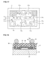
- Fig. 17 corresponds to Fig. 7(a) described in EXAMPLE 1. Structures of metal films and plating films formed on a cover layer differ from those in
- the metal films and plating films have detour portions 17s and 17t out of an original wiring direction and expanded portions 17x and 17y each having a width larger than an original line width and cover a substantially overall surface above the sealed space 13.
- the detour portions 17s and 17t intersect repeatedly above the sealed space 13.
- the expanded portions 17x and 17y expand from the original interconnection lines along a direction intersecting a wiring direction and overlap the sealed space 13.
- the piezoelectric device in EXAMPLE 2 has the structure and thus has increased strength such that the sealed space 13 does not collapse.
- inductors and capacitors are connected to resonators in parallel or series.
- circuit elements such as inductors and capacitors, are connected to input and output terminals of devices.
- the detour portions 17s and 17t in EXAMPLE 2 can be used as inductors.
- Fig. 18 shows an example of a structure having first electrodes disposed in the exterior resin 26.
- the expanded portions 17x and 17y are used as the first electrodes, and the conductive pattern 15 on the piezoelectric substrate 12 or an electrode pattern disposed in the exterior resin 26 with insulating members therebetween is used as a second electrode.
- the expanded portions 17x and 17y can be used as capacitors.
- the detour portions (17s and 17t) of the internal conductor 17, internal conductors 28 located thereabove, and an insulating material provided therebetween can constitute capacitors.
- an insulating member constituting the exterior resin 26 or another insulating material may be disposed between the internal conductors.
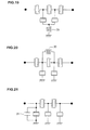
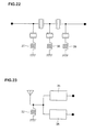
- Figs. 19, 20, 21 , and 22 each show an example of a SAW filter.
- the structure can be used as inductors 29, 30, and 37 to 39 and a capacitor 21.
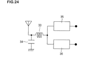
- Figs. 23 and 24 each show an example of an antenna duplexer including a transmitting SAW filter 35, a receiving SAW filter 36, and matching elements.
- the structure can be used as inductors 32 and 33 and a capacitor 34.
- a piezoelectric device in EXAMPLE 3 will be described with reference to Fig. 25 .
- the piezoelectric device in EXAMPLE 3 has substantially the same structure as that of the piezoelectric device 10 in EXAMPLE 1.
- the same components as those of the piezoelectric device 10 in EXAMPLE 1 are designated using the same reference numerals, and differences from the piezoelectric device 10 in EXAMPLE 1 will be mainly described.
- Fig. 25 corresponds to Fig. 7 described in EXAMPLE 1.
- an additional layer 24 is formed on the cover layer 22.
- a metal film 16s is formed between the cover layer 22 and the additional layer 24.
- a plating film 17q is formed on a metal film 16t located on the additional layer 24.
- the piezoelectric device in EXAMPLE 3 is produced in substantially the same way as the piezoelectric device 10 in EXAMPLE 1.
- the same steps are performed as those shown in Figs. 2 to 6 according to EXAMPLE 1. That is, a metal film 16s is formed on the cover layer 22 and connected to a via hole 17p. Subsequently, a photosensitive polyimide is applied, exposed, and developed to form the additional layer 24 having, if required, an opening.
- the metal film 16t is formed on the additional layer 24 by evaporation and lift-off. The strength of interconnection lines located on the metal film 16t is reinforced with the plating film 17q formed by electrolytic plating.
- cover-film-line processing with a laser beam, lamination of a sealing resin, laser processing, and the like are performed in the same way as in EXAMPLE 1.
- the interconnection lines on the cover layer 22 have two layers.
- the metal film 16s and 16t are disposed on substantially the overall surface above sealed space 13a and 13b, respectively.
- the sealed space 13a is reinforced with the lower metal film 16s.
- the sealed space 13b is reinforced with the upper metal film 16t and the plating film 17q.
- the interconnection metal layers with the reinforcing plating films are disposed above the sealed space.
- the use of the interconnection metal layers formed on the sealed space or the formation of the thick metal films simultaneously with the formation of the interconnection metal layers ensures the piezoelectric device having resistance to molding with no increase in costs.
- the plating films disposed above the sealed space include dummy portions expanding in a direction different from an original interconnection pattern connected to the via hole conductor.
- the dummy portions can further increase strength.
- the piezoelectric device of the present invention and the method for producing the piezoelectric device are not limited to the above-described EXAMPLES. Various changes may be made.
- the present invention is not limited to the SAW filters but may be applied to piezoelectric devices such as SAW resonators and BAW filters.
Landscapes
- Physics & Mathematics (AREA)
- Acoustics & Sound (AREA)
- Surface Acoustic Wave Elements And Circuit Networks Thereof (AREA)
- Piezo-Electric Or Mechanical Vibrators, Or Delay Or Filter Circuits (AREA)
Abstract
Description
- The present invention relates to a piezoelectric device and a method for producing the same. In particular, the present invention relates to a piezoelectric device including a piezoelectric substrate and a piezoelectric element; and a method for producing the piezoelectric device.
- In piezoelectric devices, such as resonators and filters, including piezoelectric substrates and piezoelectric films, construction in which piezoelectric vibration spaces are formed by mainly buildup structures including resins and the like has been known.
- For example, Patent Document 1 discloses that in a structure in which IDT electrodes overlaid with a cover and protruding electrodes protruding from pad electrodes, the protruding electrodes being disposed outside the cover, are disposed on a piezoelectric substrate and in which they are covered with an insulating layer and a resin layer, the IDT electrodes have improved moisture resistance because the surface of the cover is overlaid with the insulating layer composed of a Si-based compound.
-
Patent Document 2 discloses that in a structure in which spaces formed around a vibrator are sealed with spacers surrounding a vibrator, the spacers being bonded to a piezoelectric substrate, and with sealing films bonded to the spacers, the sealing films are each formed of a metal sheet or the like, and a reinforcing layer formed of a ceramic sheet or a metal sheet is disposed between the sealing films and a second armor disposed outside the sealing films. - Patent Document 3 discloses that in a structure in which a resonator element disposed on a surface of the piezoelectric substrate is covered with a resin substrate so as to be distant from the resin substrate, a metal layer is disposed on the entirety of the surface of the resin substrate facing the piezoelectric substrate so as to inhibit the permeation of water and gases passing through the resin substrate.
- Patent Document 4 discloses that input/output electrodes for connection with the SAW chip, a ground electrode, and a conductive pattern surrounding the ground electrode so as to obtain inductance are provided on the side of a mounting substrate on which a SAW chip is mounted.
- [Patent Document 1]
Japanese Unexamined Patent Application Publication No. 2002-217673 - [Patent Document 2]
Japanese Unexamined Patent Application Publication No. 6-164292 - [Patent Document 3]
Japanese Unexamined Patent Application Publication No. 2003-37471 - [Patent Document 4]
Japanese Unexamined Patent Application Publication No. 2004-165874 - As described above, such construction in which piezoelectric vibration spaces are formed by mainly buildup structures including resins and the like contributes advantageously to a reduction in profile.
- However, in the case where after a piezoelectric device sealed with a buildup structure including a resin is mounted on a circuit substrate, the resulting component is resin-molded together with another chip such as a semiconductor chip, the piezoelectric device may collapse because resin molding is generally performed under high-temperature and high-pressure conditions.
- Thus, for example, countermeasures to increase strength with the insulating layer composed of the Si-based compound described in Patent Document 1 may be taken. However, costs are inevitably increased because of an increase in the number of steps, the necessity for the insulating layer to have a thickness of at least 10 µm in order to withstand such resin molding performed under the high-temperature and high-pressure conditions, and the necessity to separately perform the formation of vias for extraction electrodes.
- In consideration of the situations, the present invention provides a piezoelectric device having resistance to molding and a method for producing the piezoelectric device with no increase in cost.
- To overcome the foregoing problems, the present invention provides a piezoelectric device having the following structure.
- A piezoelectric device includes an elemental substrate including a piezoelectric element and a conductive pattern electrically connected to the piezoelectric element disposed on at least one main surface of the elemental substrate, an insulating member disposed on the main surface side of the elemental substrate and surrounding the piezoelectric element leaving a space around the piezoelectric element, and an internal conductor disposed in the insulating member in such a manner as to be connected to the conductive pattern, and extending apart from the elemental substrate. The internal conductor includes an expanded portion expanding in a direction intersecting the wiring direction of the internal conductor or a detour portion out of the wiring direction. The expanded portion or the detour portion crosses the boundary of the space (hereinafter, referred to as a "sealed space") formed around the piezoelectric element when viewed from the direction normal to the main surface of the elemental substrate.
- The internal conductor having the above described structure can reinforce the side of the insulating member forming the periphery of the sealed space. Thus, even when a pressure is applied to the piezoelectric device from the outside during resin molding, the piezoelectric device does not collapse.
- According to this structure, the piezoelectric device has increased strength without the addition of a special step or a special component. The internal conductor is generally formed of a metal film, thus ensuring the strength of the sealed space without the inhibition of miniaturization or a reduction in profile.
- Preferably, the sealed space has a substantially rectangular shape when viewed from the direction normal to the main surface of the elemental substrate. The internal conductor has a portion intersecting at least two opposite sides of the sealed space when viewed from the direction normal to the main surface of the elemental substrate. The portion includes the expanded portion or the detour portion.
- According to the above-described structure, the expanded portion or the detour portion may intersect the sealed space alone or together with a portion of the internal conductor other than the expanded portion or the detour portion when viewed from the direction normal to the main surface of the elemental substrate.
- According to the above-described structure, the strength of the sealed space is easily ensured.
- Preferably, the sealed space has a substantially rectangular shape when viewed from the direction normal to the main surface of the elemental substrate. The internal conductor has a portion intersecting at least two adjacent sides of the sealed space when viewed from the direction normal to the main surface of the elemental substrate. The portion includes the expanded portion or the detour portion.
- According to the above-described structure, the expanded portion or the detour portion may intersect the sealed space alone or together with a portion of the internal conductor other than the expanded portion or the detour portion when viewed from the direction normal to the main surface of the elemental substrate.
- According to the above-described structure, the strength of the sealed space is easily ensured.
- Preferably, the internal conductor is disposed on 1/2 or more of the area of the sealed space when viewed from the direction normal to the main surface of the elemental substrate.
- According to the above-described structure, the strength of the sealed space is easily ensured.
- Preferably, the internal conductor is disposed on substantially the entire area of the sealed space when viewed from the direction normal to the main surface of the elemental substrate.
- According to the above-described structure, the strength is easily ensured.
- Preferably, at least a portion of the internal conductor disposed within the sealed space is formed of a plating film composed of a metal material when viewed from the direction normal to the main surface of the elemental substrate.
- According to the above-described structure, the plating film of the internal conductor is formed so as to have a large thickness, thereby ensuring the strength of the sealed space without an increase in costs.
- Preferably, the metal plating film of the internal conductor has a thickness of 10 µm or more.
- According to the above-described structure, sufficient strength can be ensured.
- Preferably, the internal conductor contains a metal material having an elastic modulus of 1.3 × 10¹¹ Pa or more.
- The internal conductor having a higher elastic modulus has more resistance to deformation and thus has higher strength, provided that the thickness is constant.
- Preferably, the internal conductor is composed of a metal material mainly containing Ni.
- Nickel satisfies requirements, such as plating properties, strength, interconnection resistance, and inexpensiveness, for the internal conductor.
- Preferably, the piezoelectric element is an element utilizing a surface acoustic wave or a bulk wave.
- In this case, it is possible to provide a piezoelectric device having resistance to molding and a high-strength package structure without an increase in costs.
- Preferably, the piezoelectric element includes the expanded portion or the detour portion used as a circuit element or part of a circuit element. The expanded portion or the detour portion may be electrically connected to the piezoelectric element.
- Preferably, the piezoelectric element includes the expanded portion or the detour portion used as an inductor. The expanded portion or the detour portion may be electrically connected to the piezoelectric element.
- Preferably, the piezoelectric element includes the expanded portion or the detour portion used as part of a capacitor. The expanded portion or the detour portion may be electrically connected to the piezoelectric element.
- In this case, a circuit element, such as an inductor or a capacitor, required to satisfy device properties can be efficiently formed while the strength of the sealed space is ensured, thereby reducing the size of the device.
- In addition, to overcome the foregoing problems, the present invention provides a method for producing a piezoelectric device as follows.
- The method for producing a piezoelectric device includes a first step of forming a piezoelectric element and a conductive pattern on at least one main surface of an elemental substrate, the conductive pattern being electrically connected to the piezoelectric element, and a second step of forming an insulating member disposed on the main surface side of the elemental substrate and surrounding the piezoelectric element leaving a space around the piezoelectric element and forming an internal conductor in the insulating member, connected to the conductive pattern, and extending apart from the elemental substrate. The second step further including a substep of forming a reinforcing portion reinforcing the strength of the space formed around the piezoelectric element simultaneously with the formation of the internal conductor in the insulating member.
- According to the method, a piezoelectric device having a high-strength package structure and resistance to molding can be provided with no increase in costs.
- According to the piezoelectric device and the method for producing the piezoelectric device, resistance to molding can be ensured without an increase in costs.
-
-
Fig. 1 is a cross-sectional view of a piezoelectric device (first embodiment). -
Fig. 2 is an explanatory drawing of a process of producing the piezoelectric device (first embodiment). -
Fig. 3 is an explanatory drawing of the process of producing the piezoelectric device (first embodiment). -
Fig. 4 is an explanatory drawing of the process of producing the piezoelectric device (first embodiment). -
Fig. 5 is an explanatory drawing of the process of producing the piezoelectric device (first embodiment). -
Fig. 6 is an explanatory drawing of the process of producing the piezoelectric device (first embodiment). -
Fig. 7 is an explanatory drawing of the process of producing the piezoelectric device (first embodiment). -
Fig. 8 is an explanatory drawing of the process of producing the piezoelectric device (first embodiment). -
Fig. 9 is an explanatory drawing of the process of producing the piezoelectric device (first embodiment). -
Fig. 10 is an explanatory drawing of the process of producing the piezoelectric device (first embodiment). -
Fig. 11 is an explanatory drawing of the process of producing the piezoelectric device (first embodiment). -
Fig. 12 is an explanatory drawing of the process of producing the piezoelectric device (first embodiment). -
Fig. 13 is an explanatory drawing of the process of producing the piezoelectric device (first embodiment). -
Fig. 14 is an explanatory drawing of the process of producing the piezoelectric device (first embodiment). -
Fig. 15 is an explanatory drawing of the process of producing the piezoelectric device (first embodiment). -
Fig. 16 is an explanatory drawing of the piezoelectric device subjected to resin molding (first embodiment). -
Fig. 17 is an explanatory drawing of a process of producing a piezoelectric device (second embodiment). -
Fig. 18 is an explanatory drawing of the process of producing the piezoelectric device (second embodiment). -
Fig. 19 is a circuit diagram of a SAW filter as an example of a piezoelectric device (second embodiment). -
Fig. 20 is a circuit diagram of a SAW filter as an example of a piezoelectric device (second embodiment). -
Fig. 21 is a circuit diagram of a SAW filter as an example of a piezoelectric device (second embodiment). -
Fig. 22 is a circuit diagram of a SAW filter as an example of a piezoelectric device (second embodiment). -
Fig. 23 is a circuit diagram of antenna duplexer (second embodiment). -
Fig. 24 is a circuit diagram of antenna duplexer (second embodiment). -
Fig. 25 is an explanatory drawing of a process of producing a piezoelectric device (third embodiment). -
- 10 SAW device (piezoelectric device)
- 12 piezoelectric substrate (elemental substrate)
- 13 sealed space
- 15 pad electrode (conductive pattern)
- 16, 16s, 16t metal film (internal conductor)
- 17 connecting member (internal conductor)
- 17q plating film (internal conductor)
- 20 support layer (insulating member)
- 22 cover (insulating member)
- 24 additional layer (insulating member)
- 26 exterior resin (insulating member)
- 28 connecting member (internal conductor)
- 29, 30, 32, 33 inductor
- 31, 34 capacitor
- 35, 36 SAW filter
- Embodiments and examples of the present invention will be described below with reference to
Figs. 1 to 25 . - A
piezoelectric device 10 according to EXAMPLE 1 will be described with reference toFigs. 1 to 16 . - Referring to
Fig. 1 that is a cross-sectional view, thepiezoelectric device 10 is a surface acoustic wave (SAW) filter. A conductive pattern including an interdigital transducer (IDT) 14 with interdigital electrodes, reflectors,pad electrodes 15, interconnection lines, and the like is formed on one main surface, i.e., a top face 12a, of apiezoelectric substrate 12. Aprotective film 11 is formed on the other main surface, i.e., abottom face 12b, of thesubstrate 12. According to desired properties, a quartz substrate, a LiTaO3 substrate, LiNbO3 substrate, a substrate including a ZnO thin film, or the like is used as thesubstrate 12. - A
support layer 20, which is a first resin portion, is formed on the top face 12a of thepiezoelectric substrate 12 and on thepad electrodes 15 so as to surround theIDT 14. Acover layer 22, which is a second resin portion, is disposed on thesupport layer 20 so as to be distant from thepiezoelectric substrate 12. Thecover layer 22 extends substantially along thepiezoelectric substrate 12. Thesupport layer 20, which is an insulating member, and thecover layer 22 constitute a sealedspace 13 enclosing theIDT 14. A surface acoustic wave propagates on a portion of the top face 12a of thepiezoelectric substrate 12 adjacent to the sealedspace 13 without limitation. - The entirety of the
cover layer 22 and the periphery of the top face 12a of thepiezoelectric substrate 12 is covered with anexterior resin 26.External terminals 19 are exposed from theexterior resin 26. Theexternal terminals 19 are electrically connected to thepad electrodes 15 throughinternal conductors underbump metal layers 19a disposed in through holes (via holes) and the like that are formed in thesupport layer 20,cover layer 22, and theexterior resin 26. Theexternal terminals 19 are electrically connected to terminals and the like of a circuit substrate when thepiezoelectric device 10 is mounted. - Referring to
Figs. 2 to 15 , a process of producing thepiezoelectric device 10 will be described below.Figs. 2 to 15 each show a portion corresponding to substantially onepiezoelectric device 10 having a final shape. In fact, a collective substrate including portions corresponding to a plurality ofpiezoelectric devices 10 two-dimensionally arranged, e.g., in a matrix, is produced. - As shown in
Fig. 2 , first wiring layers to be formed into the conductive pattern including theIDT 14, the reflectors, thepad electrodes 15, the interconnection lines, and the like are formed on thepiezoelectric substrate 12. That is, a lift-off resist pattern having openings through which the conductive pattern will be formed is formed by photolithography on thepiezoelectric substrate 12. A metal film mainly composed of Al is formed by evaporation. The resulting substrate is immersed and shaken in a stripping solution to remove the resist pattern by lift-off, thereby forming the first wiring layers. - As shown in
Fig. 3 , second wiring layers 15a are formed. That is, a resist pattern having openings which communicate with thepad electrodes 15, the interconnection lines, and the like and through which a metal film for reducing interconnection resistance will be formed is formed. Then the metal film is formed by evaporation. After lift-off, the second wiring layers 15a are formed. The metal film may be composed of Al, Cu, Ni, Au, and Pt. Alternatively, the metal film may have a multilayer structure of these metals. If plating is performed, the surface layer of each of the second wiring layers is preferably composed of Cu, Ni, Au, or Pt having satisfactory plating properties. - As shown in
Fig. 4 , thesupport layer 20, which is a first resin portion, is formed. That is, thesupport layer 20 is formed as follows: A photosensitive polyimide is applied, exposed, and developed to form a polyimide pattern having openings communicating with theIDT 14 and thesecond wiring layers 15a. After the formation of the pattern, polyimide is cured by heating. Subsequently, organic substance attached to theIDT 14 is removed with oxygen plasma.Openings 21 formed here are used as part of through holes. - Instead of polyimide, a compound having sufficiently low outgassing, a sufficiently low halogen content, having heat resistance, and strength may be used. Examples thereof include benzocyclobutene and silicone.
- As shown in
Fig. 5 , thecover layer 22, which is a second resin portion, is formed. Thecover layer 22 is formed of a polyimide film. The polyimide film has a thermoplastic polyimide resin as an adhesive layer disposed on a surface of the polyimide film. The film is laminated and bonded to thesupport layer 20 using a roller having a temperature of 100°C. Thereby, the sealedspace 13 around theIDT 14 is primarily sealed. - As shown in
Fig. 6 ,metal films 16 are formed. That is, a resist pattern having openings through which themetal films 16 will be formed is formed on thecover layer 22. A Au film having a thickness of 0.1 µm is formed by evaporation. The resist is removed by lift-off together with undesired metal films, thereby forming themetal films 16 having a target pattern. - As shown in
Fig. 7 , throughholes openings 21 in thesupport layer 20 are formed in thecover layer 22 and themetal films 16 using a laser beam. Desmearing, plasma treatment, and the like are performed to remove residues resulting from laser processing. - Referring to
Fig. 8(a) that is a plan view when viewed along line A-A inFig. 10 in the subsequent step described below and referring toFig. 8(b) that is a cross-sectional view taken along line B-B inFig. 8(a) , connectingmembers 17 are disposed on themetal films 16. The pattern of themetal films 16 substantially conforms to the pattern of the connectingmembers 17. As shown inFig. 8(a) , with respect to the pattern of themetal films 16 formed, many films are intentionally formed above the sealedspace 13. In particular, in the case where two different sides of each sealedspace 13 intersect with a corresponding one of portions indicated byreference numerals space 13 intersect with a corresponding one of portions indicated byreference numerals space 13 is effectively reinforced. The arrangement of necessary leads indicated byreference numerals reference numerals space 13 is effective in reinforcing the sealedspace 13. Expanded portions indicated byreference numerals space 13 so as to only increase the strength of the sealedspace 13, thereby improving the strength of thecover layer 22 located above the sealedspace 13. - Specifically, as shown in
Fig. 9 , the throughholes members 17 by electrolytic plating or electroless plating to form via holes. A Ni film having a thickness of 20 µm is formed on themetal films 16 disposed on thecover layer 22. The connection of the via holes and themetal films 16 with the connectingmembers 17 further increases the strength of thecover layer 22 located above the sealedspace 13. Preferably, plating films formed on themetal films 16 disposed on thecover layer 22 are each composed of a material having a large elastic modulus. Ni films are more preferred because they are easily formed by plating and each have a large elastic modulus. Each of the plating films may have a multilayer structure. Furthermore, the plating rate is relatively high. The time required for the formation of the film having a thickness of 20 µm is about 10 minutes. Thus, the plating films do not trigger an increase in costs. - As shown in
Fig. 10 , theperiphery 25 of thecover layer 22 is removed by a laser beam. Dry etching with oxygen plasma, wet etching with an etching solution, cutting with a dicing machine including a rotary blade, or the like may be performed instead of laser processing. - As shown in
Fig. 11 , theexterior resin 26 is formed. That is, an insulating epoxy-resin film is laminated. Alternatively, a liquid epoxy resin may be applied by printing to form an epoxy-resin film. Instead of the epoxy resin, an insulating material, e.g., a benzocyclobutene resin, a silicone resin, or a spin-on-glass (SOG), may be used. Subsequently, the insulating material is cured at 240°C in an oven. - As shown in
Fig. 12 , through holes (via holes) 27 are formed in theexterior resin 26 with a laser beam. As shown inFig. 13 , the via holes are filled with ametal 18 by electrolytic plating. When theexterior resin 26 is composed of a photosensitive insulating material, via processing may be performed by photolithography. Alternatively, via processing may be performed by dry etching. - As shown in
Fig. 13 , theunderbump metal layers 19a are formed. - As shown in
Fig. 14 , solder paste is applied on theunderbump metal layers 19a by printing with a metal mask. The solder paste is heated to form solder bumps serving as theexternal terminals 19. - As shown in
Fig. 15 , thepiezoelectric substrate 12 and theexterior resin 26 and thesecond wiring layers 15a located on thepiezoelectric substrate 12 are cut into individual piezoelectric device chip pieces. Thereby, piezoelectric device chip is completed. Separation may be performed by cutting with arotary blade 50, by cutting with a laser beam, or in combination of both. - For example, the resulting
piezoelectric device 10 is mounted on a glass-epoxy circuit board 2 as shown inFig. 16 . After another device such as an IC chip 6 is mounted on thecircuit board 2 in addition to thepiezoelectric device 10, a molding resin 4 is injected into a mold 8 at, for example, 180°C and 100 atm. Thereby, a module having some functions is completed. - The molding resin 4 is pressurized as indicated by arrows 5 during the above-described transfer molding. Thus, a force from the outside as indicated by
arrows 5b acts on thepiezoelectric device 10. Since thepiezoelectric device 10 is reinforced with the wiring metal layer located above the sealedspace 13, the sealedspace 13 has improved resistance to molding. The use of the internal interconnection lines on thecover layer 22 or the formation of the thick metal films (plating films) on thecover layer 22 in order to increase the strength of the sealedspace 13 simultaneously with the formation of the internal interconnection lines on thecover layer 22 ensures resistance to transfer molding with no increase in costs. - In this case, as described above, in the
piezoelectric device 10, thesupport layer 20 and thecover layer 22 above the sealedspace 13 have a buildup structure of a resin film and the like, thus facilitating a reduction in profile. Therefore, even when the piezoelectric device is mounted on a circuit board together with another device to form a module, the piezoelectric device does not cause an increase in the thickness of the module and results in the module having a sufficiently small thickness. Furthermore, the piezoelectric device can ensure strength such that the sealedspace 13 does not collapse during transfer molding. - The
piezoelectric device 10 sealed with a resin buildup structure, which facilitates a reduction in profile, ensures resistance to molding. Thus, a low-profile module can be made without an increase in costs or the use of an alumina package having a recess (cavity). - As described above, the
piezoelectric device 10 is an inexpensive, low-profile piezoelectric device sealed with, for example, the resin buildup structure and can ensure resistance to transfer molding without an increase in costs. - A piezoelectric device in EXAMPLE 2 will be described with reference to
Figs. 17 to 24 . The piezoelectric device in EXAMPLE 2 has substantially the same structure as that of thepiezoelectric device 10 in EXAMPLE 1. Hereinafter, the same components as those of thepiezoelectric device 10 in EXAMPLE 1 are designated using the same reference numerals, and differences from thepiezoelectric device 10 in EXAMPLE 1 will be mainly described. -
Fig. 17 corresponds to Fig. 7(a) described in EXAMPLE 1. Structures of metal films and plating films formed on a cover layer differ from those in - That is, the metal films and plating films have
detour portions portions 17x and 17y each having a width larger than an original line width and cover a substantially overall surface above the sealedspace 13. Thedetour portions space 13. The expandedportions 17x and 17y expand from the original interconnection lines along a direction intersecting a wiring direction and overlap the sealedspace 13. - The piezoelectric device in EXAMPLE 2 has the structure and thus has increased strength such that the sealed
space 13 does not collapse. - In SAW filters, to obtain required electrical properties, it is known that inductors and capacitors are connected to resonators in parallel or series. To match an external circuit and convert impedance, it is known that circuit elements, such as inductors and capacitors, are connected to input and output terminals of devices.
- The
detour portions -
Fig. 18 shows an example of a structure having first electrodes disposed in theexterior resin 26. The expandedportions 17x and 17y are used as the first electrodes, and theconductive pattern 15 on thepiezoelectric substrate 12 or an electrode pattern disposed in theexterior resin 26 with insulating members therebetween is used as a second electrode. In this case, the expandedportions 17x and 17y can be used as capacitors. - Furthermore, as shown in
Fig. 18 , the detour portions (17s and 17t) of theinternal conductor 17,internal conductors 28 located thereabove, and an insulating material provided therebetween can constitute capacitors. In this case, an insulating member constituting theexterior resin 26 or another insulating material may be disposed between the internal conductors. - Such a structure can be applied to various devices. For example,
Figs. 19, 20, 21 , and22 each show an example of a SAW filter. The structure can be used asinductors capacitor 21.Figs. 23 and24 each show an example of an antenna duplexer including a transmittingSAW filter 35, a receivingSAW filter 36, and matching elements. The structure can be used asinductors capacitor 34. - A piezoelectric device in EXAMPLE 3 will be described with reference to
Fig. 25 . The piezoelectric device in EXAMPLE 3 has substantially the same structure as that of thepiezoelectric device 10 in EXAMPLE 1. Hereinafter, the same components as those of thepiezoelectric device 10 in EXAMPLE 1 are designated using the same reference numerals, and differences from thepiezoelectric device 10 in EXAMPLE 1 will be mainly described. -
Fig. 25 corresponds toFig. 7 described in EXAMPLE 1. Unlike the structure in EXAMPLE 1, in the piezoelectric device in EXAMPLE 3, anadditional layer 24 is formed on thecover layer 22. Ametal film 16s is formed between thecover layer 22 and theadditional layer 24. A plating film 17q is formed on ametal film 16t located on theadditional layer 24. - The piezoelectric device in EXAMPLE 3 is produced in substantially the same way as the
piezoelectric device 10 in EXAMPLE 1. The same steps are performed as those shown inFigs. 2 to 6 according to EXAMPLE 1. That is, ametal film 16s is formed on thecover layer 22 and connected to a via hole 17p. Subsequently, a photosensitive polyimide is applied, exposed, and developed to form theadditional layer 24 having, if required, an opening. Themetal film 16t is formed on theadditional layer 24 by evaporation and lift-off. The strength of interconnection lines located on themetal film 16t is reinforced with the plating film 17q formed by electrolytic plating. Then, cover-film-line processing with a laser beam, lamination of a sealing resin, laser processing, and the like are performed in the same way as in EXAMPLE 1. - The interconnection lines on the
cover layer 22 have two layers. Themetal film space space 13a is reinforced with thelower metal film 16s. The sealedspace 13b is reinforced with theupper metal film 16t and the plating film 17q. - As described above, the interconnection metal layers with the reinforcing plating films are disposed above the sealed space. The use of the interconnection metal layers formed on the sealed space or the formation of the thick metal films simultaneously with the formation of the interconnection metal layers ensures the piezoelectric device having resistance to molding with no increase in costs.
- The plating films disposed above the sealed space include dummy portions expanding in a direction different from an original interconnection pattern connected to the via hole conductor. The dummy portions can further increase strength.
- The use of the interconnection metal layers formed above the sealed space as a circuit element or part of a circuit element results in miniaturization of the piezoelectric device.
- The piezoelectric device of the present invention and the method for producing the piezoelectric device are not limited to the above-described EXAMPLES. Various changes may be made.
- For example, the present invention is not limited to the SAW filters but may be applied to piezoelectric devices such as SAW resonators and BAW filters.
Claims (17)
- A piezoelectric device comprising:an elemental substrate including a piezoelectric element and a conductive pattern electrically connected to the piezoelectric element disposed on at least one main surface of the elemental substrate;an insulating member disposed on the main surface side of the elemental substrate and surrounding the piezoelectric element leaving a space around the piezoelectric element; andan internal conductor disposed in the insulating member in such a manner as to be connected to the conductive pattern, and extending apart from the elemental substrate,wherein the internal conductor includes an expanded portion expanding in a direction intersecting the wiring direction of the internal conductor or a detour portion out of the wiring direction, andthe expanded portion or the detour portion crosses the boundary of the space (hereinafter, referred to as a "sealed space") formed around the piezoelectric element when viewed from the direction normal to the main surface of the elemental substrate.
- The piezoelectric device according to claim 1, wherein the sealed space has a substantially rectangular shape when viewed from the direction normal to the main surface of the elemental substrate, and
wherein the internal conductor has a portion intersecting at least two opposite sides of the sealed space when viewed from the direction normal to the main surface of the elemental substrate, the portion including the expanded portion or the detour portion. - The piezoelectric device according to claim 1, wherein the sealed space has a substantially rectangular shape when viewed from the direction normal to the main surface of the elemental substrate, and
wherein the internal conductor has a portion intersecting at least two adjacent sides of the sealed space when viewed from the direction normal to the main surface of the elemental substrate, the portion including the expanded portion or the detour portion. - The piezoelectric device according to claim 1, 2, or 3, wherein the internal conductor is disposed on 1/2 or more of the area of the sealed space when viewed from the direction normal to the main surface of the elemental substrate.
- The piezoelectric device according to claim 1, 2, or 3, wherein the internal conductor is disposed on substantially the entire area of the sealed space when viewed from the direction normal to the main surface of the elemental substrate.
- The piezoelectric device according to any one of claims 1 to 5, wherein at least a portion of the internal conductor disposed within the sealed space is formed of a plating film composed of a metal material when viewed from the direction normal to the main surface of the elemental substrate.
- The piezoelectric device according to claim 6, wherein the metal plating film of the internal conductor has a thickness of 10 µm or more.
- The piezoelectric device according to any one of claims 1 to 7, wherein the internal conductor contains a metal material having an elastic modulus of 1.3 × 10¹¹ Pa or more.
- The piezoelectric device according to any one of claims 1 to 8, wherein the internal conductor is composed of a metal material mainly containing Ni.
- The piezoelectric device according to any one of claims 1 to 9, wherein the piezoelectric element is an element utilizing a surface acoustic wave or a bulk wave.
- A method for producing a piezoelectric device, comprising:a first step of forming a piezoelectric element and a conductive pattern on at least one main surface of an elemental substrate, the conductive pattern being electrically connected to the piezoelectric element; anda second step of forming an insulating member disposed on the main surface side of the elemental substrate and surrounding the piezoelectric element leaving a space around the piezoelectric element and forming an internal conductor in the insulating member, connected to the conductive pattern, and extending apart from the elemental substrate,wherein the second step further including a substep of forming a reinforcing portion reinforcing the strength of the space formed around the piezoelectric element simultaneously with the formation of the internal conductor in the insulating member.
- The piezoelectric device according to any one of claims 1 to 10, wherein the expanded portion or the detour portion is used as a circuit element or part of a circuit element.
- The piezoelectric device according to any one of claims 1 to 10, wherein the expanded portion or the detour portion is used as an inductor.
- The piezoelectric device according to any one of claims 1 to 10, wherein the expanded portion or the detour portion is used as part of a capacitor.
- The piezoelectric device according to any one of claims 1 to 10 and 12 to 14, wherein the expanded portion or the detour portion is electrically connected to the piezoelectric element.
- The piezoelectric device according to any one of claims 1 to 10 and 12 to 15, wherein the expanded portion or the detour portion is formed between different insulating member segments.
- The piezoelectric device according to any one of claims 1 to 10 and 12 to 16, wherein the expanded portion or the detour portion is formed between an insulating member segment in contact with the sealed space and having a hollow structure and an insulating member segment in contact with outer surface and forming an exterior resin.
Applications Claiming Priority (3)
| Application Number | Priority Date | Filing Date | Title |
|---|---|---|---|
| JP2005176129 | 2005-06-16 | ||
| JP2006157895 | 2006-06-06 | ||
| PCT/JP2006/311851 WO2006134928A1 (en) | 2005-06-16 | 2006-06-13 | Piezoelectric device and manufacturing method thereof |
Publications (3)
| Publication Number | Publication Date |
|---|---|
| EP1892831A1 true EP1892831A1 (en) | 2008-02-27 |
| EP1892831A4 EP1892831A4 (en) | 2009-05-06 |
| EP1892831B1 EP1892831B1 (en) | 2012-08-29 |
Family
ID=37532286
Family Applications (1)
| Application Number | Title | Priority Date | Filing Date |
|---|---|---|---|
| EP20060757286 Active EP1892831B1 (en) | 2005-06-16 | 2006-06-13 | Piezoelectric device and manufacturing method thereof |
Country Status (5)
| Country | Link |
|---|---|
| US (1) | US7427824B2 (en) |
| EP (1) | EP1892831B1 (en) |
| JP (1) | JP4586852B2 (en) |
| CN (1) | CN101107776B (en) |
| WO (1) | WO2006134928A1 (en) |
Cited By (2)
| Publication number | Priority date | Publication date | Assignee | Title |
|---|---|---|---|---|
| EP2009710A3 (en) * | 2007-06-27 | 2009-04-22 | Nihon Dempa Kogyo Co., Ltd. | Piezoelectric component and manufacturing method thereof |
| EP3288184A1 (en) * | 2016-08-25 | 2018-02-28 | General Electric Company | Embedded rf filter package structure and method of manufacturing thereof |
Families Citing this family (109)
| Publication number | Priority date | Publication date | Assignee | Title |
|---|---|---|---|---|
| KR100731509B1 (en) * | 2005-12-23 | 2007-06-21 | 주식회사 에스세라 | Surface-mounted resonators with cap means using an insulated ceramic base plate and methods of forming the same |
| JP2008135971A (en) * | 2006-11-28 | 2008-06-12 | Fujitsu Media Device Kk | Elastic wave device |
| JP5113394B2 (en) * | 2007-01-23 | 2013-01-09 | 太陽誘電株式会社 | Elastic wave device |
| JP5117083B2 (en) * | 2007-03-09 | 2013-01-09 | 太陽誘電株式会社 | Elastic wave device and manufacturing method thereof |
| JP4910953B2 (en) * | 2007-09-10 | 2012-04-04 | パナソニック株式会社 | Electronic component package structure |
| TWI360207B (en) | 2007-10-22 | 2012-03-11 | Advanced Semiconductor Eng | Chip package structure and method of manufacturing |
| WO2009057699A1 (en) * | 2007-10-30 | 2009-05-07 | Kyocera Corporation | Elastic wave device |
| WO2009078137A1 (en) * | 2007-12-14 | 2009-06-25 | Murata Manufacturing Co., Ltd. | Surface wave device and method of manufacturing the same |
| JP4468456B2 (en) * | 2008-01-07 | 2010-05-26 | 富士通メディアデバイス株式会社 | Elastic wave device and manufacturing method thereof |
| US8384272B2 (en) * | 2008-01-30 | 2013-02-26 | Kyocera Corporation | Acoustic wave device and method for production of same |
| JP5104432B2 (en) * | 2008-03-17 | 2012-12-19 | パナソニック株式会社 | Surface acoustic wave device |
| JP5104518B2 (en) * | 2008-04-22 | 2012-12-19 | パナソニック株式会社 | Surface acoustic wave device and manufacturing method thereof |
| JP5283972B2 (en) * | 2008-05-28 | 2013-09-04 | 太陽誘電株式会社 | Surface acoustic wave device |
| JP5106633B2 (en) * | 2008-06-27 | 2012-12-26 | 京セラ株式会社 | Elastic wave device |
| DE112010000861B4 (en) * | 2009-01-15 | 2016-12-15 | Murata Manufacturing Co., Ltd. | Piezoelectric device and method of manufacturing a piezoelectric device |
| JP5338396B2 (en) * | 2009-03-12 | 2013-11-13 | パナソニック株式会社 | Manufacturing method of surface acoustic wave device |
| JP5532685B2 (en) * | 2009-06-01 | 2014-06-25 | 株式会社村田製作所 | Elastic wave device |
| JP2010278971A (en) * | 2009-06-01 | 2010-12-09 | Murata Mfg Co Ltd | Elastic wave device |
| JP5521417B2 (en) * | 2009-07-15 | 2014-06-11 | パナソニック株式会社 | Elastic wave device and electronic device using the same |
| US8334737B2 (en) * | 2009-07-15 | 2012-12-18 | Panasonic Corporation | Acoustic wave device and electronic apparatus using the same |
| JP5537096B2 (en) * | 2009-08-28 | 2014-07-02 | 京セラ株式会社 | Elastic wave device and circuit board |
| WO2011065499A1 (en) * | 2009-11-27 | 2011-06-03 | 京セラ株式会社 | Acoustic wave device and method for manufacturing the same |
| CN102652394B (en) * | 2010-01-12 | 2015-05-13 | 京瓷株式会社 | Acoustic wave device |
| US8569894B2 (en) | 2010-01-13 | 2013-10-29 | Advanced Semiconductor Engineering, Inc. | Semiconductor package with single sided substrate design and manufacturing methods thereof |
| JP2011188255A (en) | 2010-03-09 | 2011-09-22 | Panasonic Corp | Acoustic wave device |
| TWI411075B (en) | 2010-03-22 | 2013-10-01 | 日月光半導體製造股份有限公司 | Semiconductor package and method of manufacturing same |
| CN102291098A (en) * | 2010-06-21 | 2011-12-21 | 湖南嘉业达电子有限公司 | Insulating moisture-proof method of chip of other piezoelectric ceramic radial vibration mode frequency device |
| JP5591163B2 (en) * | 2010-10-29 | 2014-09-17 | 京セラ株式会社 | Elastic wave device and manufacturing method thereof |
| JP5755434B2 (en) * | 2010-11-30 | 2015-07-29 | 京セラ株式会社 | Elastic wave device and manufacturing method thereof |
| CN102763328B (en) * | 2010-12-16 | 2015-12-02 | 天工松下滤波方案日本有限公司 | elastic wave device |
| US9406658B2 (en) | 2010-12-17 | 2016-08-02 | Advanced Semiconductor Engineering, Inc. | Embedded component device and manufacturing methods thereof |
| CN103415995B (en) | 2011-03-09 | 2016-08-17 | 株式会社村田制作所 | Electronic Components |
| JP5626451B2 (en) * | 2011-03-22 | 2014-11-19 | 株式会社村田製作所 | Electronic component module manufacturing method and electronic component module |
| JP5561254B2 (en) * | 2011-07-29 | 2014-07-30 | 株式会社村田製作所 | Circuit module and composite circuit module |
| WO2013128823A1 (en) * | 2012-02-28 | 2013-09-06 | パナソニック株式会社 | Elastic wave device and manufacturing method therefor |
| JP5358724B1 (en) | 2012-06-28 | 2013-12-04 | 太陽誘電株式会社 | Elastic wave device built-in module and communication apparatus |
| CN104145426B (en) | 2012-08-01 | 2017-11-28 | 株式会社村田制作所 | Electronic component and electronic component module |
| JP5122018B1 (en) * | 2012-08-10 | 2013-01-16 | 太陽誘電株式会社 | Electronic component built-in board |
| JP5521016B2 (en) * | 2012-08-31 | 2014-06-11 | 太陽誘電株式会社 | Elastic wave device |
| JP6106404B2 (en) * | 2012-10-30 | 2017-03-29 | 太陽誘電株式会社 | Electronic component module |
| CN103824932A (en) | 2012-11-15 | 2014-05-28 | 日本电波工业株式会社 | Piezoelectric component |
| JP6044643B2 (en) * | 2012-12-05 | 2016-12-14 | 株式会社村田製作所 | Method for manufacturing elastic wave device and elastic wave device |
| US9583414B2 (en) | 2013-10-31 | 2017-02-28 | Qorvo Us, Inc. | Silicon-on-plastic semiconductor device and method of making the same |
| US9812350B2 (en) | 2013-03-06 | 2017-11-07 | Qorvo Us, Inc. | Method of manufacture for a silicon-on-plastic semiconductor device with interfacial adhesion layer |
| US9209380B2 (en) * | 2013-03-08 | 2015-12-08 | Triquint Semiconductor, Inc. | Acoustic wave device |
| JP5467375B2 (en) * | 2013-03-22 | 2014-04-09 | パナソニック株式会社 | Surface acoustic wave device |
| JP2015012428A (en) * | 2013-06-28 | 2015-01-19 | 京セラ株式会社 | Acoustic wave device, electronic component module, and mobile terminal |
| KR101754200B1 (en) * | 2013-08-20 | 2017-07-05 | 가부시키가이샤 무라타 세이사쿠쇼 | Surface acoustic wave device and manufacturing method therefor |
| JP6288110B2 (en) * | 2013-12-27 | 2018-03-07 | 株式会社村田製作所 | Elastic wave device |
| CN106464231B (en) * | 2014-05-20 | 2019-02-22 | 株式会社村田制作所 | Elastic wave device and method of making the same |
| US9824951B2 (en) | 2014-09-12 | 2017-11-21 | Qorvo Us, Inc. | Printed circuit module having semiconductor device with a polymer substrate and methods of manufacturing the same |
| US10085352B2 (en) | 2014-10-01 | 2018-09-25 | Qorvo Us, Inc. | Method for manufacturing an integrated circuit package |
| US10121718B2 (en) | 2014-11-03 | 2018-11-06 | Qorvo Us, Inc. | Printed circuit module having a semiconductor device with a protective layer in place of a low-resistivity handle layer |
| KR101706257B1 (en) * | 2015-01-13 | 2017-02-13 | (주)와이솔 | Acoustic wave device |
| KR101959455B1 (en) * | 2015-03-16 | 2019-03-18 | 가부시키가이샤 무라타 세이사쿠쇼 | Surface acoustic wave device |
| US9613831B2 (en) | 2015-03-25 | 2017-04-04 | Qorvo Us, Inc. | Encapsulated dies with enhanced thermal performance |
| US9960145B2 (en) | 2015-03-25 | 2018-05-01 | Qorvo Us, Inc. | Flip chip module with enhanced properties |
| US20160343604A1 (en) | 2015-05-22 | 2016-11-24 | Rf Micro Devices, Inc. | Substrate structure with embedded layer for post-processing silicon handle elimination |
| WO2016189952A1 (en) * | 2015-05-22 | 2016-12-01 | 株式会社村田製作所 | Electronic component |
| US10276495B2 (en) | 2015-09-11 | 2019-04-30 | Qorvo Us, Inc. | Backside semiconductor die trimming |
| US10069474B2 (en) * | 2015-11-17 | 2018-09-04 | Qualcomm Incorporated | Encapsulation of acoustic resonator devices |
| US10020405B2 (en) | 2016-01-19 | 2018-07-10 | Qorvo Us, Inc. | Microelectronics package with integrated sensors |
| KR102653201B1 (en) * | 2016-03-30 | 2024-04-01 | 삼성전기주식회사 | Acoustic wave device and manufacturing method thereof |
| US10062583B2 (en) | 2016-05-09 | 2018-08-28 | Qorvo Us, Inc. | Microelectronics package with inductive element and magnetically enhanced mold compound component |
| US10784149B2 (en) | 2016-05-20 | 2020-09-22 | Qorvo Us, Inc. | Air-cavity module with enhanced device isolation |
| US10468329B2 (en) | 2016-07-18 | 2019-11-05 | Qorvo Us, Inc. | Thermally enhanced semiconductor package having field effect transistors with back-gate feature |
| US10773952B2 (en) | 2016-05-20 | 2020-09-15 | Qorvo Us, Inc. | Wafer-level package with enhanced performance |
| US10103080B2 (en) | 2016-06-10 | 2018-10-16 | Qorvo Us, Inc. | Thermally enhanced semiconductor package with thermal additive and process for making the same |
| CN109716511A (en) | 2016-08-12 | 2019-05-03 | Qorvo美国公司 | Wafer-level packaging with enhanced performance |
| SG11201901193UA (en) | 2016-08-12 | 2019-03-28 | Qorvo Us Inc | Wafer-level package with enhanced performance |
| EP4672306A2 (en) | 2016-08-12 | 2025-12-31 | Qorvo Us, Inc. | METHOD FOR MANUFACTURING A WAFER-LEVEL ENCLOSURE WITH IMPROVED PERFORMANCE |
| US10109502B2 (en) | 2016-09-12 | 2018-10-23 | Qorvo Us, Inc. | Semiconductor package with reduced parasitic coupling effects and process for making the same |
| US10090339B2 (en) | 2016-10-21 | 2018-10-02 | Qorvo Us, Inc. | Radio frequency (RF) switch |
| US10749518B2 (en) | 2016-11-18 | 2020-08-18 | Qorvo Us, Inc. | Stacked field-effect transistor switch |
| US10068831B2 (en) | 2016-12-09 | 2018-09-04 | Qorvo Us, Inc. | Thermally enhanced semiconductor package and process for making the same |
| WO2018110464A1 (en) * | 2016-12-15 | 2018-06-21 | 株式会社村田製作所 | Elastic wave device |
| US20180234075A1 (en) * | 2017-02-14 | 2018-08-16 | Samsung Electro-Mechanics Co., Ltd. | Bulk acoustic wave resonator |
| US10804950B2 (en) | 2017-03-22 | 2020-10-13 | Kyocera Corporation | Acoustic wave device, multiplexer, and communication apparatus |
| US10483248B2 (en) * | 2017-03-23 | 2019-11-19 | Skyworks Solutions, Inc. | Wafer level chip scale filter packaging using semiconductor wafers with through wafer vias |
| KR102295454B1 (en) * | 2017-04-25 | 2021-08-27 | 가부시키가이샤 무라타 세이사쿠쇼 | Electronic components and modules having the same |
| KR102414843B1 (en) * | 2017-05-22 | 2022-06-30 | 삼성전기주식회사 | Acoustic wave device and method of manufacturing method thereofthe same) |
| US10490471B2 (en) | 2017-07-06 | 2019-11-26 | Qorvo Us, Inc. | Wafer-level packaging for enhanced performance |
| US10366972B2 (en) | 2017-09-05 | 2019-07-30 | Qorvo Us, Inc. | Microelectronics package with self-aligned stacked-die assembly |
| US10784233B2 (en) | 2017-09-05 | 2020-09-22 | Qorvo Us, Inc. | Microelectronics package with self-aligned stacked-die assembly |
| WO2019078234A1 (en) * | 2017-10-19 | 2019-04-25 | 株式会社村田製作所 | Acoustic wave device |
| US11152363B2 (en) | 2018-03-28 | 2021-10-19 | Qorvo Us, Inc. | Bulk CMOS devices with enhanced performance and methods of forming the same utilizing bulk CMOS process |
| WO2019195428A1 (en) | 2018-04-04 | 2019-10-10 | Qorvo Us, Inc. | Gallium-nitride-based module with enhanced electrical performance and process for making the same |
| US12046505B2 (en) | 2018-04-20 | 2024-07-23 | Qorvo Us, Inc. | RF devices with enhanced performance and methods of forming the same utilizing localized SOI formation |
| US10804246B2 (en) | 2018-06-11 | 2020-10-13 | Qorvo Us, Inc. | Microelectronics package with vertically stacked dies |
| US12165951B2 (en) | 2018-07-02 | 2024-12-10 | Qorvo Us, Inc. | RF devices with enhanced performance and methods of forming the same |
| US11894824B2 (en) | 2018-08-30 | 2024-02-06 | Skyworks Solutions, Inc. | Laser-marked packaged surface acoustic wave devices |
| US11069590B2 (en) | 2018-10-10 | 2021-07-20 | Qorvo Us, Inc. | Wafer-level fan-out package with enhanced performance |
| US10964554B2 (en) | 2018-10-10 | 2021-03-30 | Qorvo Us, Inc. | Wafer-level fan-out package with enhanced performance |
| US11646242B2 (en) | 2018-11-29 | 2023-05-09 | Qorvo Us, Inc. | Thermally enhanced semiconductor package with at least one heat extractor and process for making the same |
| US12057374B2 (en) | 2019-01-23 | 2024-08-06 | Qorvo Us, Inc. | RF devices with enhanced performance and methods of forming the same |
| US12046570B2 (en) | 2019-01-23 | 2024-07-23 | Qorvo Us, Inc. | RF devices with enhanced performance and methods of forming the same |
| US12125825B2 (en) | 2019-01-23 | 2024-10-22 | Qorvo Us, Inc. | RF devices with enhanced performance and methods of forming the same |
| US12046483B2 (en) | 2019-01-23 | 2024-07-23 | Qorvo Us, Inc. | RF devices with enhanced performance and methods of forming the same |
| US11387157B2 (en) | 2019-01-23 | 2022-07-12 | Qorvo Us, Inc. | RF devices with enhanced performance and methods of forming the same |
| EP3915134A1 (en) | 2019-01-23 | 2021-12-01 | Qorvo US, Inc. | Rf semiconductor device and manufacturing method thereof |
| JP6780718B2 (en) * | 2019-02-28 | 2020-11-04 | 株式会社大真空 | Piezoelectric vibration device |
| JP2021016035A (en) * | 2019-07-10 | 2021-02-12 | 株式会社村田製作所 | Acoustic wave device |
| US12074086B2 (en) | 2019-11-01 | 2024-08-27 | Qorvo Us, Inc. | RF devices with nanotube particles for enhanced performance and methods of forming the same |
| US11646289B2 (en) | 2019-12-02 | 2023-05-09 | Qorvo Us, Inc. | RF devices with enhanced performance and methods of forming the same |
| US11923238B2 (en) | 2019-12-12 | 2024-03-05 | Qorvo Us, Inc. | Method of forming RF devices with enhanced performance including attaching a wafer to a support carrier by a bonding technique without any polymer adhesive |
| US12129168B2 (en) | 2019-12-23 | 2024-10-29 | Qorvo Us, Inc. | Microelectronics package with vertically stacked MEMS device and controller device |
| CN116583949A (en) | 2020-12-11 | 2023-08-11 | Qorvo美国公司 | Multi-level 3D stacked package and method of forming same |
| US12062571B2 (en) | 2021-03-05 | 2024-08-13 | Qorvo Us, Inc. | Selective etching process for SiGe and doped epitaxial silicon |
| CN116405004A (en) * | 2023-04-06 | 2023-07-07 | 见闻录(浙江)半导体有限公司 | Resonator and component, filter, electronic device, manufacturing method and packaging structure |
Family Cites Families (25)
| Publication number | Priority date | Publication date | Assignee | Title |
|---|---|---|---|---|
| US4028646A (en) * | 1974-12-30 | 1977-06-07 | Matsushita Electric Industrial Co., Ltd. | Elastic surface wave devices and method for making the same |
| JPH06164292A (en) | 1992-11-25 | 1994-06-10 | Tdk Corp | Piezoelectric component and its manufacture |
| US5939817A (en) * | 1994-09-22 | 1999-08-17 | Nippon Electric Co | Surface acoustic wave device |
| JP3301262B2 (en) * | 1995-03-28 | 2002-07-15 | 松下電器産業株式会社 | Surface acoustic wave device |
| DE69718693T2 (en) | 1996-03-08 | 2003-11-27 | Matsushita Electric Industrial Co., Ltd. | Electronic component and manufacturing process |
| JP2000353934A (en) * | 1999-06-10 | 2000-12-19 | Murata Mfg Co Ltd | Surface acoustic wave device |
| JP4377500B2 (en) * | 1999-12-24 | 2009-12-02 | 京セラ株式会社 | Surface acoustic wave device and method of manufacturing surface acoustic wave device |
| JP4382945B2 (en) * | 2000-01-31 | 2009-12-16 | 京セラ株式会社 | Surface acoustic wave device |
| JP4691787B2 (en) | 2001-01-15 | 2011-06-01 | パナソニック株式会社 | SAW device |
| US6969945B2 (en) * | 2001-02-06 | 2005-11-29 | Matsushita Electric Industrial Co., Ltd. | Surface acoustic wave device, method for manufacturing, and electronic circuit device |
| JP3974346B2 (en) * | 2001-03-30 | 2007-09-12 | 富士通メディアデバイス株式会社 | Surface acoustic wave device |
| JP2003046017A (en) * | 2001-05-25 | 2003-02-14 | Kyocera Corp | Electronic component storage package and method of manufacturing the same |
| JP3772702B2 (en) | 2001-07-23 | 2006-05-10 | 松下電器産業株式会社 | Manufacturing method of surface acoustic wave device |
| JP3818147B2 (en) | 2001-12-18 | 2006-09-06 | 松下電器産業株式会社 | SAW device manufacturing method |
| JP2004129224A (en) | 2002-07-31 | 2004-04-22 | Murata Mfg Co Ltd | Piezoelectric component and method of manufacturing the same |
| JP2004129223A (en) * | 2002-07-31 | 2004-04-22 | Murata Mfg Co Ltd | Piezoelectric component and method of manufacturing the same |
| JP4093021B2 (en) | 2002-11-12 | 2008-05-28 | エプソントヨコム株式会社 | Surface mount type SAW filter |
| JP2004248243A (en) * | 2002-12-19 | 2004-09-02 | Murata Mfg Co Ltd | Electronic component and method of manufacturing the same |
| EP1600530B1 (en) * | 2003-03-04 | 2011-05-11 | Fujitsu Limited | (001)-orientated perovskite film formation method and device having perovskite film |
| JP2004274574A (en) * | 2003-03-11 | 2004-09-30 | Toyo Commun Equip Co Ltd | Surface acoustic wave device and method of manufacturing the same |
| JP4000081B2 (en) * | 2003-03-12 | 2007-10-31 | 京セラ株式会社 | Diplexer built-in wiring board |
| JP4341622B2 (en) * | 2003-06-26 | 2009-10-07 | 株式会社村田製作所 | Surface acoustic wave device |
| JP2005033689A (en) * | 2003-07-11 | 2005-02-03 | Toyo Commun Equip Co Ltd | Surface acoustic wave device and manufacturing method thereof |
| JP2005079694A (en) * | 2003-08-28 | 2005-03-24 | Kyocera Corp | Duplexer |
| JP4210958B2 (en) * | 2004-07-14 | 2009-01-21 | 株式会社村田製作所 | Piezoelectric device |
-
2006
- 2006-06-13 EP EP20060757286 patent/EP1892831B1/en active Active
- 2006-06-13 WO PCT/JP2006/311851 patent/WO2006134928A1/en not_active Ceased
- 2006-06-13 CN CN2006800030208A patent/CN101107776B/en active Active
- 2006-06-13 JP JP2007521306A patent/JP4586852B2/en active Active
-
2007
- 2007-07-06 US US11/774,023 patent/US7427824B2/en active Active
Cited By (4)
| Publication number | Priority date | Publication date | Assignee | Title |
|---|---|---|---|---|
| EP2009710A3 (en) * | 2007-06-27 | 2009-04-22 | Nihon Dempa Kogyo Co., Ltd. | Piezoelectric component and manufacturing method thereof |
| US7913367B2 (en) | 2007-06-27 | 2011-03-29 | Nihon Dempa Kogyo Co., Ltd. | Method of manufacturing a piezoelectric component |
| EP3288184A1 (en) * | 2016-08-25 | 2018-02-28 | General Electric Company | Embedded rf filter package structure and method of manufacturing thereof |
| US10333493B2 (en) | 2016-08-25 | 2019-06-25 | General Electric Company | Embedded RF filter package structure and method of manufacturing thereof |
Also Published As
| Publication number | Publication date |
|---|---|
| US7427824B2 (en) | 2008-09-23 |
| JPWO2006134928A1 (en) | 2009-01-08 |
| EP1892831A4 (en) | 2009-05-06 |
| WO2006134928A1 (en) | 2006-12-21 |
| US20070252481A1 (en) | 2007-11-01 |
| EP1892831B1 (en) | 2012-08-29 |
| CN101107776B (en) | 2010-05-19 |
| JP4586852B2 (en) | 2010-11-24 |
| CN101107776A (en) | 2008-01-16 |
Similar Documents
| Publication | Publication Date | Title |
|---|---|---|
| EP1892831B1 (en) | Piezoelectric device and manufacturing method thereof | |
| EP3288184B1 (en) | Embedded rf filter package structure and method of manufacturing thereof | |
| JP5117083B2 (en) | Elastic wave device and manufacturing method thereof | |
| US7586240B2 (en) | Acoustic wave device | |
| US8736149B2 (en) | Electronic component with metal plate above element and fabrication method of the same, and electronic device including the same | |
| JP6311724B2 (en) | Electronic component module | |
| JP6555270B2 (en) | Filter parts with passive elements and high-frequency modules | |
| US8748755B2 (en) | Electronic component, electronic device, and method for manufacturing the electronic component | |
| US9197190B2 (en) | Electronic component module | |
| EP1772962A1 (en) | Surface acoustic wave device and fabrication method therefor | |
| US7102272B2 (en) | Piezoelectric component and method for manufacturing the same | |
| JP6385883B2 (en) | Module and module manufacturing method | |
| JP5873311B2 (en) | Elastic wave device and multilayer substrate | |
| KR102295454B1 (en) | Electronic components and modules having the same | |
| CN121749940A (en) | Module with elastic wave device and its manufacturing method | |
| US20250105816A1 (en) | Solidly-mounted transversely-excited film bulk acoustic device | |
| JP4910953B2 (en) | Electronic component package structure | |
| JP2024171533A (en) | Acoustic Wave Devices | |
| JP5315642B2 (en) | Electronic component package |
Legal Events
| Date | Code | Title | Description |
|---|---|---|---|
| PUAI | Public reference made under article 153(3) epc to a published international application that has entered the european phase |
Free format text: ORIGINAL CODE: 0009012 |
|
| 17P | Request for examination filed |
Effective date: 20070704 |
|
| AK | Designated contracting states |
Kind code of ref document: A1 Designated state(s): AT BE BG CH CY CZ DE DK EE ES FI FR GB GR HU IE IS IT LI LT LU LV MC NL PL PT RO SE SI SK TR |
|
| DAX | Request for extension of the european patent (deleted) | ||
| DAX | Request for extension of the european patent (deleted) | ||
| A4 | Supplementary search report drawn up and despatched |
Effective date: 20090406 |
|
| RIC1 | Information provided on ipc code assigned before grant |
Ipc: H03H 9/05 20060101AFI20090331BHEP Ipc: H03H 9/72 20060101ALI20090331BHEP Ipc: H03H 3/08 20060101ALI20090331BHEP |
|
| 17Q | First examination report despatched |
Effective date: 20090717 |
|
| REG | Reference to a national code |
Ref country code: DE Ref legal event code: R079 Ref document number: 602006031741 Country of ref document: DE Free format text: PREVIOUS MAIN CLASS: H03H0009250000 Ipc: H03H0009050000 |
|
| GRAP | Despatch of communication of intention to grant a patent |
Free format text: ORIGINAL CODE: EPIDOSNIGR1 |
|
| RIC1 | Information provided on ipc code assigned before grant |
Ipc: H03H 3/08 20060101ALI20120210BHEP Ipc: H03H 9/10 20060101ALI20120210BHEP Ipc: H03H 9/05 20060101AFI20120210BHEP Ipc: H03H 9/72 20060101ALI20120210BHEP |
|
| GRAS | Grant fee paid |
Free format text: ORIGINAL CODE: EPIDOSNIGR3 |
|
| GRAA | (expected) grant |
Free format text: ORIGINAL CODE: 0009210 |
|
| AK | Designated contracting states |
Kind code of ref document: B1 Designated state(s): AT BE BG CH CY CZ DE DK EE ES FI FR GB GR HU IE IS IT LI LT LU LV MC NL PL PT RO SE SI SK TR |
|
| REG | Reference to a national code |
Ref country code: GB Ref legal event code: FG4D |
|
| REG | Reference to a national code |
Ref country code: CH Ref legal event code: EP |
|
| REG | Reference to a national code |
Ref country code: AT Ref legal event code: REF Ref document number: 573513 Country of ref document: AT Kind code of ref document: T Effective date: 20120915 |
|
| REG | Reference to a national code |
Ref country code: IE Ref legal event code: FG4D |
|
| REG | Reference to a national code |
Ref country code: DE Ref legal event code: R096 Ref document number: 602006031741 Country of ref document: DE Effective date: 20121018 |
|
| REG | Reference to a national code |
Ref country code: AT Ref legal event code: MK05 Ref document number: 573513 Country of ref document: AT Kind code of ref document: T Effective date: 20120829 |
|
| REG | Reference to a national code |
Ref country code: NL Ref legal event code: VDEP Effective date: 20120829 |
|
| REG | Reference to a national code |
Ref country code: LT Ref legal event code: MG4D Effective date: 20120829 |
|
| PG25 | Lapsed in a contracting state [announced via postgrant information from national office to epo] |
Ref country code: FI Free format text: LAPSE BECAUSE OF FAILURE TO SUBMIT A TRANSLATION OF THE DESCRIPTION OR TO PAY THE FEE WITHIN THE PRESCRIBED TIME-LIMIT Effective date: 20120829 Ref country code: IS Free format text: LAPSE BECAUSE OF FAILURE TO SUBMIT A TRANSLATION OF THE DESCRIPTION OR TO PAY THE FEE WITHIN THE PRESCRIBED TIME-LIMIT Effective date: 20121229 Ref country code: CY Free format text: LAPSE BECAUSE OF FAILURE TO SUBMIT A TRANSLATION OF THE DESCRIPTION OR TO PAY THE FEE WITHIN THE PRESCRIBED TIME-LIMIT Effective date: 20120829 Ref country code: AT Free format text: LAPSE BECAUSE OF FAILURE TO SUBMIT A TRANSLATION OF THE DESCRIPTION OR TO PAY THE FEE WITHIN THE PRESCRIBED TIME-LIMIT Effective date: 20120829 Ref country code: LT Free format text: LAPSE BECAUSE OF FAILURE TO SUBMIT A TRANSLATION OF THE DESCRIPTION OR TO PAY THE FEE WITHIN THE PRESCRIBED TIME-LIMIT Effective date: 20120829 |
|
| PG25 | Lapsed in a contracting state [announced via postgrant information from national office to epo] |
Ref country code: SE Free format text: LAPSE BECAUSE OF FAILURE TO SUBMIT A TRANSLATION OF THE DESCRIPTION OR TO PAY THE FEE WITHIN THE PRESCRIBED TIME-LIMIT Effective date: 20120829 Ref country code: SI Free format text: LAPSE BECAUSE OF FAILURE TO SUBMIT A TRANSLATION OF THE DESCRIPTION OR TO PAY THE FEE WITHIN THE PRESCRIBED TIME-LIMIT Effective date: 20120829 Ref country code: PT Free format text: LAPSE BECAUSE OF FAILURE TO SUBMIT A TRANSLATION OF THE DESCRIPTION OR TO PAY THE FEE WITHIN THE PRESCRIBED TIME-LIMIT Effective date: 20121231 Ref country code: BE Free format text: LAPSE BECAUSE OF FAILURE TO SUBMIT A TRANSLATION OF THE DESCRIPTION OR TO PAY THE FEE WITHIN THE PRESCRIBED TIME-LIMIT Effective date: 20120829 Ref country code: GR Free format text: LAPSE BECAUSE OF FAILURE TO SUBMIT A TRANSLATION OF THE DESCRIPTION OR TO PAY THE FEE WITHIN THE PRESCRIBED TIME-LIMIT Effective date: 20121130 Ref country code: LV Free format text: LAPSE BECAUSE OF FAILURE TO SUBMIT A TRANSLATION OF THE DESCRIPTION OR TO PAY THE FEE WITHIN THE PRESCRIBED TIME-LIMIT Effective date: 20120829 |
|
| PG25 | Lapsed in a contracting state [announced via postgrant information from national office to epo] |
Ref country code: DK Free format text: LAPSE BECAUSE OF FAILURE TO SUBMIT A TRANSLATION OF THE DESCRIPTION OR TO PAY THE FEE WITHIN THE PRESCRIBED TIME-LIMIT Effective date: 20120829 Ref country code: CZ Free format text: LAPSE BECAUSE OF FAILURE TO SUBMIT A TRANSLATION OF THE DESCRIPTION OR TO PAY THE FEE WITHIN THE PRESCRIBED TIME-LIMIT Effective date: 20120829 Ref country code: NL Free format text: LAPSE BECAUSE OF FAILURE TO SUBMIT A TRANSLATION OF THE DESCRIPTION OR TO PAY THE FEE WITHIN THE PRESCRIBED TIME-LIMIT Effective date: 20120829 Ref country code: ES Free format text: LAPSE BECAUSE OF FAILURE TO SUBMIT A TRANSLATION OF THE DESCRIPTION OR TO PAY THE FEE WITHIN THE PRESCRIBED TIME-LIMIT Effective date: 20121210 Ref country code: RO Free format text: LAPSE BECAUSE OF FAILURE TO SUBMIT A TRANSLATION OF THE DESCRIPTION OR TO PAY THE FEE WITHIN THE PRESCRIBED TIME-LIMIT Effective date: 20120829 Ref country code: EE Free format text: LAPSE BECAUSE OF FAILURE TO SUBMIT A TRANSLATION OF THE DESCRIPTION OR TO PAY THE FEE WITHIN THE PRESCRIBED TIME-LIMIT Effective date: 20120829 |
|
| PG25 | Lapsed in a contracting state [announced via postgrant information from national office to epo] |
Ref country code: PL Free format text: LAPSE BECAUSE OF FAILURE TO SUBMIT A TRANSLATION OF THE DESCRIPTION OR TO PAY THE FEE WITHIN THE PRESCRIBED TIME-LIMIT Effective date: 20120829 Ref country code: IT Free format text: LAPSE BECAUSE OF FAILURE TO SUBMIT A TRANSLATION OF THE DESCRIPTION OR TO PAY THE FEE WITHIN THE PRESCRIBED TIME-LIMIT Effective date: 20120829 Ref country code: SK Free format text: LAPSE BECAUSE OF FAILURE TO SUBMIT A TRANSLATION OF THE DESCRIPTION OR TO PAY THE FEE WITHIN THE PRESCRIBED TIME-LIMIT Effective date: 20120829 |
|
| PLBE | No opposition filed within time limit |
Free format text: ORIGINAL CODE: 0009261 |
|
| STAA | Information on the status of an ep patent application or granted ep patent |
Free format text: STATUS: NO OPPOSITION FILED WITHIN TIME LIMIT |
|
| PG25 | Lapsed in a contracting state [announced via postgrant information from national office to epo] |
Ref country code: BG Free format text: LAPSE BECAUSE OF FAILURE TO SUBMIT A TRANSLATION OF THE DESCRIPTION OR TO PAY THE FEE WITHIN THE PRESCRIBED TIME-LIMIT Effective date: 20121129 |
|
| 26N | No opposition filed |
Effective date: 20130530 |
|
| REG | Reference to a national code |
Ref country code: DE Ref legal event code: R097 Ref document number: 602006031741 Country of ref document: DE Effective date: 20130530 |
|
| PG25 | Lapsed in a contracting state [announced via postgrant information from national office to epo] |
Ref country code: MC Free format text: LAPSE BECAUSE OF FAILURE TO SUBMIT A TRANSLATION OF THE DESCRIPTION OR TO PAY THE FEE WITHIN THE PRESCRIBED TIME-LIMIT Effective date: 20120829 |
|
| REG | Reference to a national code |
Ref country code: CH Ref legal event code: PL |
|
| GBPC | Gb: european patent ceased through non-payment of renewal fee |
Effective date: 20130613 |
|
| REG | Reference to a national code |
Ref country code: IE Ref legal event code: MM4A |
|
| REG | Reference to a national code |
Ref country code: FR Ref legal event code: ST Effective date: 20140228 |
|
| PG25 | Lapsed in a contracting state [announced via postgrant information from national office to epo] |
Ref country code: IE Free format text: LAPSE BECAUSE OF NON-PAYMENT OF DUE FEES Effective date: 20130613 Ref country code: GB Free format text: LAPSE BECAUSE OF NON-PAYMENT OF DUE FEES Effective date: 20130613 Ref country code: CH Free format text: LAPSE BECAUSE OF NON-PAYMENT OF DUE FEES Effective date: 20130630 Ref country code: LI Free format text: LAPSE BECAUSE OF NON-PAYMENT OF DUE FEES Effective date: 20130630 |
|
| PG25 | Lapsed in a contracting state [announced via postgrant information from national office to epo] |
Ref country code: FR Free format text: LAPSE BECAUSE OF NON-PAYMENT OF DUE FEES Effective date: 20130701 |
|
| PG25 | Lapsed in a contracting state [announced via postgrant information from national office to epo] |
Ref country code: TR Free format text: LAPSE BECAUSE OF FAILURE TO SUBMIT A TRANSLATION OF THE DESCRIPTION OR TO PAY THE FEE WITHIN THE PRESCRIBED TIME-LIMIT Effective date: 20120829 |
|
| PG25 | Lapsed in a contracting state [announced via postgrant information from national office to epo] |
Ref country code: LU Free format text: LAPSE BECAUSE OF NON-PAYMENT OF DUE FEES Effective date: 20130613 Ref country code: HU Free format text: LAPSE BECAUSE OF FAILURE TO SUBMIT A TRANSLATION OF THE DESCRIPTION OR TO PAY THE FEE WITHIN THE PRESCRIBED TIME-LIMIT; INVALID AB INITIO Effective date: 20060613 |
|
| REG | Reference to a national code |
Ref country code: DE Ref legal event code: R082 Ref document number: 602006031741 Country of ref document: DE Representative=s name: CBDL PATENTANWAELTE GBR, DE Ref country code: DE Ref legal event code: R082 Ref document number: 602006031741 Country of ref document: DE Representative=s name: CBDL PATENTANWAELTE EGBR, DE |
|
| PGFP | Annual fee paid to national office [announced via postgrant information from national office to epo] |
Ref country code: DE Payment date: 20250618 Year of fee payment: 20 |