EP1886540B1 - Leuchtschirm zum beleuchten oder anzeigen von bildern mit einer zusammengesetzten transparenten oberen elektrode - Google Patents
Leuchtschirm zum beleuchten oder anzeigen von bildern mit einer zusammengesetzten transparenten oberen elektrode Download PDFInfo
- Publication number
- EP1886540B1 EP1886540B1 EP06755219A EP06755219A EP1886540B1 EP 1886540 B1 EP1886540 B1 EP 1886540B1 EP 06755219 A EP06755219 A EP 06755219A EP 06755219 A EP06755219 A EP 06755219A EP 1886540 B1 EP1886540 B1 EP 1886540B1
- Authority
- EP
- European Patent Office
- Prior art keywords
- upper electrode
- layer
- conductive layer
- diodes
- common
- Prior art date
- Legal status (The legal status is an assumption and is not a legal conclusion. Google has not performed a legal analysis and makes no representation as to the accuracy of the status listed.)
- Active
Links
Images
Classifications
-
- H—ELECTRICITY
- H05—ELECTRIC TECHNIQUES NOT OTHERWISE PROVIDED FOR
- H05B—ELECTRIC HEATING; ELECTRIC LIGHT SOURCES NOT OTHERWISE PROVIDED FOR; CIRCUIT ARRANGEMENTS FOR ELECTRIC LIGHT SOURCES, IN GENERAL
- H05B33/00—Electroluminescent light sources
- H05B33/12—Light sources with substantially two-dimensional radiating surfaces
- H05B33/26—Light sources with substantially two-dimensional radiating surfaces characterised by the composition or arrangement of the conductive material used as an electrode
-
- H—ELECTRICITY
- H10—SEMICONDUCTOR DEVICES; ELECTRIC SOLID-STATE DEVICES NOT OTHERWISE PROVIDED FOR
- H10K—ORGANIC ELECTRIC SOLID-STATE DEVICES
- H10K50/00—Organic light-emitting devices
- H10K50/80—Constructional details
- H10K50/805—Electrodes
- H10K50/81—Anodes
-
- H—ELECTRICITY
- H10—SEMICONDUCTOR DEVICES; ELECTRIC SOLID-STATE DEVICES NOT OTHERWISE PROVIDED FOR
- H10F—INORGANIC SEMICONDUCTOR DEVICES SENSITIVE TO INFRARED RADIATION, LIGHT, ELECTROMAGNETIC RADIATION OF SHORTER WAVELENGTH OR CORPUSCULAR RADIATION
- H10F77/00—Constructional details of devices covered by this subclass
- H10F77/20—Electrodes
- H10F77/244—Electrodes made of transparent conductive layers, e.g. transparent conductive oxide [TCO] layers
- H10F77/247—Electrodes made of transparent conductive layers, e.g. transparent conductive oxide [TCO] layers comprising indium tin oxide [ITO]
-
- H—ELECTRICITY
- H10—SEMICONDUCTOR DEVICES; ELECTRIC SOLID-STATE DEVICES NOT OTHERWISE PROVIDED FOR
- H10K—ORGANIC ELECTRIC SOLID-STATE DEVICES
- H10K50/00—Organic light-emitting devices
- H10K50/10—OLEDs or polymer light-emitting diodes [PLED]
- H10K50/11—OLEDs or polymer light-emitting diodes [PLED] characterised by the electroluminescent [EL] layers
- H10K50/125—OLEDs or polymer light-emitting diodes [PLED] characterised by the electroluminescent [EL] layers specially adapted for multicolour light emission, e.g. for emitting white light
- H10K50/13—OLEDs or polymer light-emitting diodes [PLED] characterised by the electroluminescent [EL] layers specially adapted for multicolour light emission, e.g. for emitting white light comprising stacked EL layers within one EL unit
-
- H—ELECTRICITY
- H10—SEMICONDUCTOR DEVICES; ELECTRIC SOLID-STATE DEVICES NOT OTHERWISE PROVIDED FOR
- H10K—ORGANIC ELECTRIC SOLID-STATE DEVICES
- H10K50/00—Organic light-emitting devices
- H10K50/80—Constructional details
- H10K50/805—Electrodes
- H10K50/81—Anodes
- H10K50/816—Multilayers, e.g. transparent multilayers
-
- H—ELECTRICITY
- H10—SEMICONDUCTOR DEVICES; ELECTRIC SOLID-STATE DEVICES NOT OTHERWISE PROVIDED FOR
- H10K—ORGANIC ELECTRIC SOLID-STATE DEVICES
- H10K50/00—Organic light-emitting devices
- H10K50/80—Constructional details
- H10K50/805—Electrodes
- H10K50/82—Cathodes
-
- H—ELECTRICITY
- H10—SEMICONDUCTOR DEVICES; ELECTRIC SOLID-STATE DEVICES NOT OTHERWISE PROVIDED FOR
- H10K—ORGANIC ELECTRIC SOLID-STATE DEVICES
- H10K50/00—Organic light-emitting devices
- H10K50/80—Constructional details
- H10K50/805—Electrodes
- H10K50/82—Cathodes
- H10K50/828—Transparent cathodes, e.g. comprising thin metal layers
-
- H—ELECTRICITY
- H10—SEMICONDUCTOR DEVICES; ELECTRIC SOLID-STATE DEVICES NOT OTHERWISE PROVIDED FOR
- H10K—ORGANIC ELECTRIC SOLID-STATE DEVICES
- H10K59/00—Integrated devices, or assemblies of multiple devices, comprising at least one organic light-emitting element covered by group H10K50/00
- H10K59/10—OLED displays
- H10K59/12—Active-matrix OLED [AMOLED] displays
-
- H—ELECTRICITY
- H10—SEMICONDUCTOR DEVICES; ELECTRIC SOLID-STATE DEVICES NOT OTHERWISE PROVIDED FOR
- H10N—ELECTRIC SOLID-STATE DEVICES NOT OTHERWISE PROVIDED FOR
- H10N30/00—Piezoelectric or electrostrictive devices
- H10N30/704—Piezoelectric or electrostrictive devices based on piezoelectric or electrostrictive films or coatings
- H10N30/706—Piezoelectric or electrostrictive devices based on piezoelectric or electrostrictive films or coatings characterised by the underlying bases, e.g. substrates
- H10N30/708—Intermediate layers, e.g. barrier, adhesion or growth control buffer layers
-
- H—ELECTRICITY
- H10—SEMICONDUCTOR DEVICES; ELECTRIC SOLID-STATE DEVICES NOT OTHERWISE PROVIDED FOR
- H10K—ORGANIC ELECTRIC SOLID-STATE DEVICES
- H10K2102/00—Constructional details relating to the organic devices covered by this subclass
- H10K2102/301—Details of OLEDs
- H10K2102/302—Details of OLEDs of OLED structures
- H10K2102/3023—Direction of light emission
- H10K2102/3026—Top emission
-
- H—ELECTRICITY
- H10—SEMICONDUCTOR DEVICES; ELECTRIC SOLID-STATE DEVICES NOT OTHERWISE PROVIDED FOR
- H10K—ORGANIC ELECTRIC SOLID-STATE DEVICES
- H10K59/00—Integrated devices, or assemblies of multiple devices, comprising at least one organic light-emitting element covered by group H10K50/00
- H10K59/80—Constructional details
- H10K59/805—Electrodes
- H10K59/8051—Anodes
-
- H—ELECTRICITY
- H10—SEMICONDUCTOR DEVICES; ELECTRIC SOLID-STATE DEVICES NOT OTHERWISE PROVIDED FOR
- H10K—ORGANIC ELECTRIC SOLID-STATE DEVICES
- H10K59/00—Integrated devices, or assemblies of multiple devices, comprising at least one organic light-emitting element covered by group H10K50/00
- H10K59/80—Constructional details
- H10K59/805—Electrodes
- H10K59/8052—Cathodes
- H10K59/80524—Transparent cathodes, e.g. comprising thin metal layers
Definitions
- the invention relates to illumination or image display panels comprising a network of organic electroluminescent diodes supported by a substrate.
- each diode comprises an organic electroluminescent layer interposed between a lower electrode in contact with the substrate and an upper electrode which is transparent to the light emitted by this organic electroluminescent layer.
- This is so-called “upward emission” panels.
- the upper electrodes are cathodes (so-called “classical” diode structure) or anodes (so-called “reverse” structure).
- Electrodes there are generally other organic layers, such as injection and hole or electron transport layers, and / or light extraction optimization layers, in particular by resonance effect in the optical cavities between the electrodes.
- organic layers such as injection and hole or electron transport layers, and / or light extraction optimization layers, in particular by resonance effect in the optical cavities between the electrodes.
- upper electrodes are common to at least a plurality of diodes and comprise a conductive oxide layer, generally a mixed indium tin oxide (ITO) or a mixed oxide of indium and zinc (IZO).
- ITO indium tin oxide
- IZO mixed oxide of indium and zinc
- the document US 5969474 proposes to insert a buffer layer between the organic layers of the diodes and the transparent conductive oxide layer; this buffer layer is intended to protect the organic layers during the deposition of the conductive oxide layer, in particular to prevent its oxidation.
- a buffer layer material proposes a metallic conductive material based on titanium, chromium or tantalum, or a nitride of this metal.
- upper electrodes are common to a plurality of diodes and comprise a first metal conductive layer of thickness less than or equal to 20 nm, and a second conductive layer made of ITO or IZO, in contact with this first layer; this second layer generally has a thickness greater than or equal to 50 nm, and therefore greater than that of the first layer.
- this buffer layer remains very low, that is to say less than 20 nm; when using nitrides specifically (Example 2 of this document), the thickness is then only 5 nm to maintain a sufficiently high conductivity and transparency.
- An object of the invention is to provide a different and more economical solution to limit the risk of degradation of the organic layers during the deposition of transparent upper electrodes.
- the subject of the invention is an illumination or image display panel comprising a network of organic electroluminescent diodes supported by a substrate, at least one network of electrodes lower in contact with the substrate and a network of electrodes. upper electrodes, wherein each diode comprises an organic electroluminescent layer which is interposed between a lower electrode and an upper electrode, which itself is transparent to the light emitted by this diode, wherein at least one of said upper electrodes is common to a plurality of diodes and comprises a first conductive layer and a second conductive layer, and an insulating and transparent buffer layer interposed between these two conductive layers, wherein, the active zone of each diode being defined as the electroluminescent organic layer surface of this diode which is in direct contact with both a lower electrode and an upper electrode, for each said upper electrode common to a plurality of diodes, said buffer layer is pierced with windows which provide areas of direct contact between the two conductive layers of this common electrode, these contact areas being disjoint active
- the windows of the buffer layer are generally openings or "holes" made in this layer; note that in the panels described in the documents US 6172459 and US 6140763 , the buffer layers do not have windows or openings and therefore areas where the two conductive layers of the upper electrode are in direct contact with each other, without intermediate buffer layer; indeed, such direct contact is not necessary to establish a conductive bridge since the buffer layer itself is conductive; there are no more windows or openings made in the buffer layers described in the document US5739545 , in particular in ZnSe or ZnS, since, again, the buffer layers are conductive through its grain boundaries.
- the first conductive layer of each upper electrode common to several diodes is in contact with the organic electroluminescent layer.
- each diode is defined more precisely as the superposition zone of the lower electrode and of the upper electrode of this diode; it is therefore only in this zone of superposition that the organic electroluminescent layer is subjected to an electric field when the diode is energized and emits light; outside these active areas, there is no light emission.
- Each overlap region that is to say crossing or superposition, a lower electrode and an upper electrode, therefore corresponds to a diode; the active zone of this diode therefore corresponds to the electroluminescent organic layer surface of this diode which is in direct contact with both this lower electrode and this upper electrode, which is able to transmit the light emitted by this diode.
- said direct contact zones are superimposed with no active zone of the diodes having an upper electrode in common; which means that the windows or openings made in the buffer layer, which correspond to the contact areas between the two conductive layers of the upper electrode considered, are located outside the active zones; thus, if the deposition of the second conductive layer at the location of these contact areas causes degradation of the underlying organic layers, such degradation is not troublesome since it occurs outside the active areas of the diodes.
- the organic electroluminescent layer of the diodes may be common to several diodes.
- the upper electrode array may have only one electrode which is then common to all the diodes.
- the diodes of the panel are "upward" emission because the upper electrodes are transparent, at least at the locations of the diodes. These electrodes may also be semi-transparent, for example to modify the intrinsic emission colorimetry of the diodes, and / or to adjust the optical cavity effects between the electrodes so as to improve the light extraction.
- the buffer layer has an insulating character; preferably, for each said upper electrode, the surface conductivity of the buffer layer is less than one-tenth of the surface conductivity of the second layer conductive of this upper electrode; the surface conductivity of a layer means the conductivity of a square surface element of this layer; thus, in the case of a buffer layer of nitride-based material as in Example 2 of the document US5969474 the thickness of the buffer layer will be much greater than 5 nm; it is precisely because of the low surface conductivity of the buffer layer that areas of direct contact between the two conductive layers of the upper electrode are necessary, to ensure a conduction bridge; to note that in the document US5739545 , the conductive bridging between the two conductive layers of the upper electrode is ensured through the intermediate buffer layer (ZnSe in particular) and not by direct contact zones as in the invention; preferably, for each common upper electrode, the surface conductivity of the buffer layer is less than the surface conductivity of the first conductive layer of this electrode; preferably
- the buffer layer organic materials can be used, at least if they meet the low conductivity criteria above: Spiro TAD, Spiro TTB, NPB, TPD, BCP, or Bphen. It is important that the thickness of the organic material is sufficient to effectively provide the protective function of the underlying organic layers.
- the material of the buffer layer is inorganic, which makes an advantageous contribution to the encapsulation of the diodes; preferably, this material is selected from the group consisting of oxide, nitride, and silicon oxynitride, and tantalum oxide: SiOx, SiNy, TaOz., where 0 ⁇ x ⁇ 2; 0 ⁇ y ⁇ 1.33, 0 ⁇ z ⁇ 2.5.
- the electric current is transmitted between the two conductive layers of the same upper electrode via the direct contact zones which, according to the invention, are located between the diodes, more precisely between the surfaces. active or emissive diodes.
- this buffer layer covers the contact areas between the organic electroluminescent layer and the lower electrode of the diodes, this buffer layer is able to effectively protect the active zones, that is to say emissive, organic layers during the deposition the second conductive layer of the upper electrodes, especially when this deposition is carried out under energetic conditions which could degrade the organic layers in the absence of protection.
- the first conductive layer can be in direct contact with the entire surface of the organic layers, thus ensuring within these layers an electric field which is homogeneous over the entire surface. , from in order to obtain a homogeneous electroluminescent emission on this surface.
- this buffer layer is partitioned into disjoint buffer elements so that the windows or openings in the buffer layer instead form a continuous surface.
- the material of said second conductive layer is based on oxide: it is therefore transparent conductive oxide ("OTC").
- OTC transparent conductive oxide
- ITO indium tin oxide
- IZO mixed indium zinc oxide
- ITO indium tin oxide
- IZO mixed indium zinc oxide
- the deposition conditions of such oxides could degrade the organic layers in the absence of protection provided by the buffer elements.
- an advantage to using these mixed oxides is that they effectively protect the organic electroluminescent layer of the diodes against the risk of deterioration, in particular by oxygen and / or water vapor of the atmosphere and thus provide a function encapsulation.
- the thickness of the second conductive layer (33) is greater than or equal to 100 nm. Such a thickness makes it possible to reinforce the encapsulation function provided by the second conductive layer.
- the material of said first conductive layer is metallic.
- the thickness of this first conductive layer is greater than 1 nm and less than or equal to 20 nm.
- Such a low thickness makes it possible to ensure transparency, especially when the material of this layer is metallic.
- Such a small thickness generally makes it possible to ensure sufficient conductance on the surface of a diode or of a few diodes, but generally does not allow this first layer alone to ensure sufficient conductance to the whole of the upper electrode when it is common to a large plurality of diodes, which makes the second conductive layer even more useful.
- the thickness of the second conductive layer is greater than the thickness of the first conductive layer.
- the surface conductivity of the second conductive layer is greater than the surface conductivity of the first conductive layer.
- the second layer provides a uniform distribution of current over the entire surface of the panel.
- surface conductivity of a layer means the conductivity of a square surface element of this layer. Added to the choice of a metallic material, therefore very conductive, for the first layer and a conductive oxide-based material, so little conductive, for the second layer, such a criterion implies that the thickness of the second layer is much higher than that of the first layer.
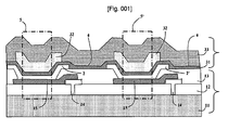
- a rigid plate 11 of insulating material supports a network of control circuits and diode supply , called “pixel circuits", each having an output 14 connected to a lower electrode 15, which is preferably metallic and reflective.
- This rigid plate generally supports several electrically insulating layers, including a first insulating layer 12, in particular for isolating the components of the pixel circuits from one another; and a second isolation layer 13 for separating the diodes and insulating the lower electrodes of the upper electrodes outside the emitting surfaces of the diodes. At the location of the diodes, this second insulating layer 13 is pierced with windows revealing the surface of the lower electrodes 15.
- this substrate integrates other unrepresented electrode arrays, in particular electrodes for the control, by example selection and addressing, pixel circuits.
- the lower electrodes 15 are generally arranged in rows and columns, depending on the arrangement of the diodes to be obtained on the panel.
- an electroluminescent organic layer is deposited on the set of lower electrodes 15, by a physical deposition method such as vacuum evaporation.
- an electroluminescent organic layer is deposited on adjacent columns.
- masks are used.
- the organic layers 2, 2 ' are subdivided into a plurality of sub-layers, in particular injection and charge transport sublayers (electrons or holes), a light-emitting underlayer per se, and, where appropriate charge-back sublayers to limit recombination of non-radiative charges.
- injection and charge transport sub-layers doped organic materials are used which make it possible to widen the range of materials that can be used for the electrodes and that make it possible to increase the thickness in order to obtain a planarization effect.
- first full metal conductive layer 31 of thickness less than or equal to 20 nm, but greater than 1 nm so as to cover the entire active surface of the substrate.
- This first conductive layer is continuous, of approximately homogeneous thickness, and without intentional holes or windows.
- the same masks can be used as for the deposition of the organic layers, which requires three deposition operations; it is also possible to use a specific mask that makes it possible to deposit in a single operation; this mask may have openings covering several diodes, or even columns or entire lines of diodes; in the case of a mask having only a diode opening, this opening may be larger or smaller than that used for the deposition of the organic layers, depending on the organic layer area that is to be protected.
- an electrically insulating and transparent material is chosen adapted to obtain effective protection of the organic layers 2, 2 'during the subsequent deposition of the second conductive layer.
- the thickness of the elements of the buffer layer 32 is also adapted for this purpose, without risk here to see the transparency decrease since the material used is transparent.
- transparent material is meant a material transmitting at least part of the electroluminescent emission spectrum of the organic layer that it covers. According to one variant of the invention, this material can also serve as an optical filter, in particular for adapting the emission spectrum and the colorimetry of the diodes.
- the material chosen for these elements of the buffer layer 32 can be deposited without risk of deterioration of the underlying organic layers 2, 2 '.
- a mineral material is preferably chosen, which provides a better protection of the underlying organic layers than an organic material; preferably, a material is chosen that can be deposited in so-called "soft" conditions that do not risk degrading the underlying organic layers, that is to say a material which, for its deposition, does not require a substrate temperature greater than 50 ° C and the energy of the particles that arise on the substrate is, during the deposition, less than 100 eV; preferably, a material having a refractive index greater than 2 is chosen to improve the light extraction rate of the upper electrode.
- a silicon oxide of formula SiOx, where 0 ⁇ x ⁇ 2, or a silicon nitride SiNy 'where 0 ⁇ y ⁇ 1.33, or an oxynitride is preferably chosen. of silicon, or tantalum oxide TaOz.
- the values of the indices x, y or z are adapted in a manner known per se for the buffer material to have a refractive index greater than 2.
- Zinc selenide (ZnSe) is preferably chosen from the refractive index is greater than 2 and which further has the advantage of being easily evaporable thermally.
- insulating and transparent inorganic materials may be used for the buffer layer 32 without departing from the invention, such as halides or chalcogenides of alkaline or alkaline earth elements.
- the thickness of the buffer layer is adapted in a manner known per se to obtain the desired level of protection, with regard to the risks of degradation of the underlying organic layers; in practice, it will generally lead to thicknesses greater than 20 nm; in practice, the surface conductivity of this buffer layer will then be less than the surface conductivity of the second conductive layer 33, subsequently deposited, which makes it necessary for the direct contact zones according to the invention to be between the two conductive layers of the upper electrode. ; preferably, the surface conductivity of this buffer layer will be less than one tenth of the surface conductivity of the second conductive layer 33.
- a second full conductive layer 33 with a thickness greater than 20 nm, so as to cover the entire active surface of the substrate.
- This second conductive layer is also continuous, of approximately homogeneous thickness, and without intentional holes or windows.
- this second conductive layer 33 a material based on ITO or IZO deposited by vacuum cathode sputtering is used.
- the first conductive layer 31, the buffer layer 32 and the second conductive layer 33 thus form here an upper electrode 3 which is common to all the diodes of the panel supported by the substrate 1.
- the second conductive layer 33 of this upper electrode is intended to distribute the supply current to each of the diodes via the first conductive layer 32 and the contact areas 4 between these layers, which correspond to the windows or openings in the buffer layer 32. .
- the thickness of the second conductive layer 33 is greater than that of the first conductive layer 31.
- the thickness of the second conductive layer 33 is adapted so that the surface conductivity of this layer is at least ten times greater than that of the first layer 31, which ensures an efficient and homogeneous distribution of the diode power supply.
- the surface conductivity of the insulating elements of the buffer layer 32 is generally less than one tenth of that of the first conductive layer.
- the elements of the buffer layer may be distributed in disjoint pads, one per diode, or one element for a set of diodes, or in continuous strips each covering a line or a column of diodes, or Other configurations, as long as the arrangement of these elements of the buffer layer household between diodes of the surface contact areas sufficient to effectively and uniformly ensure the distribution of the current as previously described.
- disjoint buffer layer elements instead of depositing disjoint buffer layer elements as previously described, it is also possible to consider depositing a "full-layer" buffer layer with windows opening between the diodes to provide areas of direct contact with the first contact layer 31.
- each lower electrode is generally common to a row of diodes, and each upper electrode is generally common to a column of diodes, or vice versa.
- the invention applies equally well to cases where the lower electrodes are anodes and the upper electrodes of the cathodes, than to the inverse cases where the lower electrodes are cathodes and the upper electrodes of the anodes.
Landscapes
- Physics & Mathematics (AREA)
- Optics & Photonics (AREA)
- Engineering & Computer Science (AREA)
- Microelectronics & Electronic Packaging (AREA)
- Electroluminescent Light Sources (AREA)
- Devices For Indicating Variable Information By Combining Individual Elements (AREA)
Claims (10)
- Beleuchtungs- oder Bildanzeigeschirm mit einem Gitter aus von einem Substrat (1) getragenen elektrolumineszenten organischen Dioden (5, 5'), mindestens einem Gitter aus unteren Elektroden (15) in Kontakt mit dem Substrat und einem Gitter aus oberen Elektroden (3), bei dem- jede Diode (5, 5') eine elektrolumineszente organische Schicht (2, 2') aufweist, die zwischen einer unteren Elektrode (15) und einer oberen Elektrode (3), welche selbst für das von dieser Diode emittierte Licht durchsichtig ist, angeordnet ist,- mindestens eine (3) der oberen Elektroden einer Vielzahl von Dioden (5, 5') gemeinsam ist und eine erste leitende Schicht (31) in Kontakt mit der elektrolumineszenten organischen Schicht (2, 2') und eine zweite leitende Schicht (33) und eine transparente, zwischen diesen zwei leitenden Schichten (31, 33) angeordnete Pufferschicht (32) umfasst, dadurch gekennzeichnet, dass bei jeder einer Vielzahl von Dioden gemeinsamen oberen Elektrode (3) die Pufferschicht (32) mit Fenstern durchbrochen ist, die Bereiche mit direktem Kontakt (4) zwischen der ersten und der zweiten leitenden Schicht (31, 33) dieser gemeinsamen Elektrode (3) bilden.
- Beleuchtungs- oder Bildanzeigeschirm nach Anspruch 1, dadurch gekennzeichnet, dass der aktive Bereich jeder Diode als der Bereich definiert ist, in dem sich bei jeder oberen Elektrode (3) die untere Elektrode und die obere Elektrode dieser Diode überlagern, wobei die Bereiche direkten Kontakts (4) sich mit keinem aktiven Bereich der Dioden, denen die obere Elektrode gemeinsam ist, überlagern.
- Beleuchtungs- oder Bildanzeigeschirm nach einem der vorstehenden Ansprüche, dadurch gekennzeichnet, dass bei jeder oberen Elektrode (3) die Oberflächenleitfähigkeit der zweiten leitenden Schicht (33) die Oberflächenleitfähigkeit der ersten leitenden Schicht (31) übersteigt und die Oberflächenleitfähigkeit der Pufferschicht geringer ist als ein Zehntel der Oberflächenleitfähigkeit der zweiten leitenden Schicht (33) der oberen Elektrode (3).
- Beleuchtungs- oder Bildanzeigeschirm nach einem der vorstehenden Ansprüche, dadurch gekennzeichnet, dass bei jeder gemeinsamen oberen Elektrode (3) das Material der Pufferschicht aus der Gruppe aus Oxid, Nitrid, Silicium-Oxinitrid und Tantaloxid gewählt ist.
- Beleuchtungs- oder Bildanzeigeschirm nach einem der vorstehenden Ansprüche, dadurch gekennzeichnet, dass bei jeder gemeinsamen oberen Elektrode (3) das Material der zweiten leitenden Schicht (33) auf Oxidbasis ist.
- Beleuchtungs- oder Bildanzeigeschirm nach Anspruch 5, dadurch gekennzeichnet, dass das Oxid aus der Gruppe aus Mischoxid aus Indium und Zinn (ITO) und Mischoxid aus Indium und Zink (IZO) gewählt ist.
- Beleuchtungs- oder Bildanzeigeschirm nach Anspruch 5 oder 6, dadurch gekennzeichnet, dass die Dicke der zweiten leitenden Schicht (33) größer als oder gleich 100 nm ist.
- Beleuchtungs- oder Bildanzeigeschirm nach einem der vorstehenden Ansprüche, dadurch gekennzeichnet, dass bei jeder gemeinsamen oberen Elektrode (3) das Material der ersten leitenden Schicht (31) metallisch ist.
- Beleuchtungs- oder Bildanzeigeschirm nach Anspruch 8, dadurch gekennzeichnet, dass die Dicke der ersten leitenden Schicht (31) größer als 1 nm und kleiner als oder gleich 20 nm ist.
- Beleuchtungs- oder Bildanzeigeschirm nach einem der vorstehenden Ansprüche, dadurch gekennzeichnet, dass bei jeder gemeinsamen oberen Elektrode (3) die Dicke der zweiten leitenden Schicht (33) größer als die Dicke der ersten leitenden Schicht (31) ist.
Applications Claiming Priority (2)
| Application Number | Priority Date | Filing Date | Title |
|---|---|---|---|
| FR0551338 | 2005-05-23 | ||
| PCT/EP2006/062355 WO2006125735A1 (fr) | 2005-05-23 | 2006-05-16 | Panneau electroluminescent d'eclairage ou d'affichage d'images dotee d'une electrode superieure transparente composite |
Publications (2)
| Publication Number | Publication Date |
|---|---|
| EP1886540A1 EP1886540A1 (de) | 2008-02-13 |
| EP1886540B1 true EP1886540B1 (de) | 2010-08-11 |
Family
ID=35539676
Family Applications (1)
| Application Number | Title | Priority Date | Filing Date |
|---|---|---|---|
| EP06755219A Active EP1886540B1 (de) | 2005-05-23 | 2006-05-16 | Leuchtschirm zum beleuchten oder anzeigen von bildern mit einer zusammengesetzten transparenten oberen elektrode |
Country Status (7)
| Country | Link |
|---|---|
| US (1) | US8063559B2 (de) |
| EP (1) | EP1886540B1 (de) |
| JP (1) | JP5214440B2 (de) |
| KR (1) | KR101292144B1 (de) |
| CN (1) | CN101180922B (de) |
| DE (1) | DE602006016109D1 (de) |
| WO (1) | WO2006125735A1 (de) |
Families Citing this family (8)
| Publication number | Priority date | Publication date | Assignee | Title |
|---|---|---|---|---|
| WO2011064700A1 (en) * | 2009-11-27 | 2011-06-03 | Koninklijke Philips Electronics N.V. | Strengthened counter electrode of electroluminescent devices |
| JP2011141981A (ja) * | 2010-01-06 | 2011-07-21 | Toppan Printing Co Ltd | 有機エレクトロルミネッセンス素子およびその製造方法 |
| GB201200823D0 (en) * | 2012-01-18 | 2012-02-29 | Cambridge Display Tech Ltd | Electroluminescence |
| KR20140142501A (ko) * | 2013-06-04 | 2014-12-12 | 삼성디스플레이 주식회사 | 표시 장치 및 그 제조 방법 |
| JP2017072812A (ja) * | 2015-10-09 | 2017-04-13 | 株式会社ジャパンディスプレイ | 表示装置 |
| KR102491880B1 (ko) * | 2016-06-16 | 2023-01-27 | 삼성디스플레이 주식회사 | 유기 발광 표시 장치 및 그 제조 방법 |
| CN112840456A (zh) * | 2018-10-11 | 2021-05-25 | 株式会社半导体能源研究所 | 摄像装置及识别装置 |
| CN114530568A (zh) * | 2022-01-21 | 2022-05-24 | 广州新视界光电科技有限公司 | 一种oled发光模组及其制作方法和显示装置 |
Family Cites Families (22)
| Publication number | Priority date | Publication date | Assignee | Title |
|---|---|---|---|---|
| KR0165867B1 (ko) * | 1995-01-21 | 1999-04-15 | 김은영 | 백색발광용 전계발광소자 및 그 제조방법 |
| JPH10125469A (ja) * | 1996-10-24 | 1998-05-15 | Tdk Corp | 有機el発光素子 |
| US5739545A (en) | 1997-02-04 | 1998-04-14 | International Business Machines Corporation | Organic light emitting diodes having transparent cathode structures |
| US6172459B1 (en) * | 1998-07-28 | 2001-01-09 | Eastman Kodak Company | Electron-injecting layer providing a modified interface between an organic light-emitting structure and a cathode buffer layer |
| JP4713010B2 (ja) * | 2000-05-08 | 2011-06-29 | 株式会社半導体エネルギー研究所 | 発光装置及びその作製方法 |
| US6608449B2 (en) | 2000-05-08 | 2003-08-19 | Semiconductor Energy Laboratory Co., Ltd. | Luminescent apparatus and method of manufacturing the same |
| CN1142708C (zh) * | 2001-04-29 | 2004-03-17 | 清华大学 | 单层有机电致发光器件及其制备方法 |
| JP4152665B2 (ja) * | 2001-07-11 | 2008-09-17 | 株式会社半導体エネルギー研究所 | 発光装置及びその作製方法 |
| US6750609B2 (en) * | 2001-08-22 | 2004-06-15 | Xerox Corporation | OLEDs having light absorbing electrode |
| JP2003092192A (ja) * | 2001-09-18 | 2003-03-28 | Matsushita Electric Ind Co Ltd | 有機エレクトロルミネッセンス表示装置およびその製造方法 |
| JP2003203783A (ja) * | 2001-10-26 | 2003-07-18 | Semiconductor Energy Lab Co Ltd | 発光装置 |
| AU2002347476A1 (en) * | 2001-12-10 | 2003-06-23 | Koninklijke Philips Electronics N.V. | El display device and method of manufacturing the same |
| US6815723B2 (en) * | 2001-12-28 | 2004-11-09 | Semiconductor Energy Laboratory Co., Ltd. | Light emitting device, method of manufacturing the same, and manufacturing apparatus therefor |
| JP4627966B2 (ja) * | 2002-01-24 | 2011-02-09 | 株式会社半導体エネルギー研究所 | 発光装置およびその作製方法 |
| JP4260494B2 (ja) * | 2002-02-26 | 2009-04-30 | 株式会社フジクラ | 透明電極用基材の製法、光電変換素子の製法、及び色素増感太陽電池の製法 |
| CA2412379A1 (en) * | 2002-11-22 | 2004-05-22 | Luxell Technolgies Inc. | Transparent-cathode for top-emission organic light-emitting diodes |
| JP3859155B2 (ja) * | 2003-03-06 | 2006-12-20 | 富士電機ホールディングス株式会社 | 有機el素子およびその製造方法 |
| JP4428005B2 (ja) * | 2003-09-04 | 2010-03-10 | セイコーエプソン株式会社 | 電気光学装置、電気光学装置の製造方法、及び電子機器 |
| US7411223B2 (en) * | 2003-09-15 | 2008-08-12 | General Electric Company | Compound electrodes for electronic devices |
| JP4716699B2 (ja) * | 2003-09-30 | 2011-07-06 | 三洋電機株式会社 | 有機elパネル |
| US8018152B2 (en) * | 2004-05-20 | 2011-09-13 | Semiconductor Energy Laboratory Co., Ltd. | Light-emitting element including intermediate conductive layer having a hole-injection layer with an island-like structure |
| US8241467B2 (en) * | 2004-08-10 | 2012-08-14 | Global Oled Technology Llc | Making a cathode structure for OLEDs |
-
2006
- 2006-05-16 US US11/920,446 patent/US8063559B2/en active Active
- 2006-05-16 CN CN2006800181142A patent/CN101180922B/zh active Active
- 2006-05-16 WO PCT/EP2006/062355 patent/WO2006125735A1/fr not_active Ceased
- 2006-05-16 EP EP06755219A patent/EP1886540B1/de active Active
- 2006-05-16 JP JP2008512803A patent/JP5214440B2/ja active Active
- 2006-05-16 DE DE602006016109T patent/DE602006016109D1/de active Active
- 2006-05-16 KR KR1020077025975A patent/KR101292144B1/ko active Active
Also Published As
| Publication number | Publication date |
|---|---|
| JP2009506480A (ja) | 2009-02-12 |
| US8063559B2 (en) | 2011-11-22 |
| US20090302755A1 (en) | 2009-12-10 |
| DE602006016109D1 (de) | 2010-09-23 |
| EP1886540A1 (de) | 2008-02-13 |
| WO2006125735A1 (fr) | 2006-11-30 |
| CN101180922B (zh) | 2010-10-06 |
| CN101180922A (zh) | 2008-05-14 |
| KR101292144B1 (ko) | 2013-08-09 |
| JP5214440B2 (ja) | 2013-06-19 |
| KR20080022542A (ko) | 2008-03-11 |
Similar Documents
| Publication | Publication Date | Title |
|---|---|---|
| EP2345097B1 (de) | Verfahren zum einkapseln einer organischen optoelektronischen anordnung | |
| FR3091035A1 (fr) | PROCEDE DE FABRICATION D’UN PIXEL D’UN MICRO-ECRAN A OLEDs | |
| EP3529834B1 (de) | Anzeigevorrichtung und verfahren zur herstellung solch einer vorrichtung | |
| EP3776661A1 (de) | Elektrolumineszente vorrichtung mit verbesserter auflösung und zuverlässigkeit | |
| FR2913146A1 (fr) | Electrode discontinue, dispositif electroluminescent organique l'incorporant, et leurs fabrications | |
| FR2868210A1 (fr) | Dispositif electroluminescent organique et procede de fabrication de celui-ci | |
| KR20060050803A (ko) | 표시 장치 및 그 제조 방법 | |
| EP1886540B1 (de) | Leuchtschirm zum beleuchten oder anzeigen von bildern mit einer zusammengesetzten transparenten oberen elektrode | |
| EP2311093A2 (de) | Polychromatische elektronische displayanordnung mit elektrolumineszenzschirm | |
| EP2399306A1 (de) | Transparentes substrat für fotonische bauelemente | |
| EP4176468B1 (de) | Optoelektronische vorrichtung und verfahren zur herstellung einer optoelektronischen vorrichtung | |
| FR2903225A1 (fr) | Dispositif d'affichage par electroluminescence organique et son procede de fabrication | |
| EP1456831B1 (de) | Bildanzeigetafel in form einer matrix von elektrolumineszenten zellen mit überbrückung und durch ein lichtempfindliches element erhaltenem speichereffekt | |
| EP1994579B1 (de) | Organische leuchtdiode mit mehrschichtiger transparenter elektrode | |
| FR2887684A1 (fr) | Diode electroluminescente dont l'une des electrodes est multicouche en carbone amorphe | |
| WO2014013183A1 (fr) | Electrode supportee transparente pour oled | |
| FR2888345A1 (fr) | Dispositif d'affichage a ecran plat et procede de fabrication de ce dernier | |
| EP4327369B1 (de) | Verfahren zur herstellung einer optoelektronischen vorrichtung mit einem stapel aus mehreren quantentöpfen | |
| FR2966275A1 (fr) | Écran et dispositif de camouflage associe | |
| EP3921871B1 (de) | Elektrolumineszente anzeigevorrichtung | |
| FR2859811A1 (fr) | Panneau electroluminescent d'eclairage ou de visualisation d'images dote d'electrodes superieures transparentes renforcees par des grilles | |
| WO2022096798A1 (fr) | Dispositif d'affichage a empilement technologique hybride | |
| EP4362093A1 (de) | Lichtemittierende vorrichtung und lichtempfänger | |
| FR2859823A1 (fr) | Panneau organique electroluminescent comprenant une couche d'extraction de lumiere incorporant des particules reflechissantes | |
| WO2020084250A1 (fr) | Procédé de fabrication d'un pixel d'un micro-écran à oleds |
Legal Events
| Date | Code | Title | Description |
|---|---|---|---|
| PUAI | Public reference made under article 153(3) epc to a published international application that has entered the european phase |
Free format text: ORIGINAL CODE: 0009012 |
|
| 17P | Request for examination filed |
Effective date: 20071204 |
|
| AK | Designated contracting states |
Kind code of ref document: A1 Designated state(s): DE FR GB |
|
| RAP1 | Party data changed (applicant data changed or rights of an application transferred) |
Owner name: THOMSON LICENSING |
|
| DAX | Request for extension of the european patent (deleted) | ||
| RBV | Designated contracting states (corrected) |
Designated state(s): DE FR GB |
|
| 17Q | First examination report despatched |
Effective date: 20080725 |
|
| RIN1 | Information on inventor provided before grant (corrected) |
Inventor name: VAUFREY, DAVID Inventor name: RACINE, BENOIT Inventor name: HAAS, GUNTHER |
|
| RIN1 | Information on inventor provided before grant (corrected) |
Inventor name: RACINE, BENOIT Inventor name: HAAS, GUNTHER Inventor name: VAUFREY, DAVID |
|
| GRAP | Despatch of communication of intention to grant a patent |
Free format text: ORIGINAL CODE: EPIDOSNIGR1 |
|
| RAP1 | Party data changed (applicant data changed or rights of an application transferred) |
Owner name: THOMSON LICENSING |
|
| RIN1 | Information on inventor provided before grant (corrected) |
Inventor name: RACINE, BENOIT Inventor name: HAAS, GUNTHER Inventor name: VAUFREY, DAVID |
|
| GRAS | Grant fee paid |
Free format text: ORIGINAL CODE: EPIDOSNIGR3 |
|
| GRAA | (expected) grant |
Free format text: ORIGINAL CODE: 0009210 |
|
| AK | Designated contracting states |
Kind code of ref document: B1 Designated state(s): DE FR GB |
|
| REG | Reference to a national code |
Ref country code: GB Ref legal event code: FG4D Free format text: NOT ENGLISH |
|
| REF | Corresponds to: |
Ref document number: 602006016109 Country of ref document: DE Date of ref document: 20100923 Kind code of ref document: P |
|
| PLBE | No opposition filed within time limit |
Free format text: ORIGINAL CODE: 0009261 |
|
| STAA | Information on the status of an ep patent application or granted ep patent |
Free format text: STATUS: NO OPPOSITION FILED WITHIN TIME LIMIT |
|
| 26N | No opposition filed |
Effective date: 20110512 |
|
| REG | Reference to a national code |
Ref country code: DE Ref legal event code: R097 Ref document number: 602006016109 Country of ref document: DE Effective date: 20110512 |
|
| REG | Reference to a national code |
Ref country code: FR Ref legal event code: PLFP Year of fee payment: 11 |
|
| REG | Reference to a national code |
Ref country code: FR Ref legal event code: PLFP Year of fee payment: 12 |
|
| REG | Reference to a national code |
Ref country code: DE Ref legal event code: R082 Ref document number: 602006016109 Country of ref document: DE Representative=s name: DEHNS, DE Ref country code: DE Ref legal event code: R082 Ref document number: 602006016109 Country of ref document: DE Representative=s name: DEHNS PATENT AND TRADEMARK ATTORNEYS, DE Ref country code: DE Ref legal event code: R082 Ref document number: 602006016109 Country of ref document: DE Representative=s name: HOFSTETTER, SCHURACK & PARTNER PATENT- UND REC, DE |
|
| REG | Reference to a national code |
Ref country code: FR Ref legal event code: PLFP Year of fee payment: 13 |
|
| REG | Reference to a national code |
Ref country code: DE Ref legal event code: R082 Ref document number: 602006016109 Country of ref document: DE Representative=s name: DEHNS, DE Ref country code: DE Ref legal event code: R081 Ref document number: 602006016109 Country of ref document: DE Owner name: INTERDIGITAL CE PATENT HOLDINGS SAS, FR Free format text: FORMER OWNER: THOMSON LICENSING, ISSY-LES-MOULINEAUX, FR Ref country code: DE Ref legal event code: R082 Ref document number: 602006016109 Country of ref document: DE Representative=s name: DEHNS PATENT AND TRADEMARK ATTORNEYS, DE |
|
| REG | Reference to a national code |
Ref country code: GB Ref legal event code: 732E Free format text: REGISTERED BETWEEN 20190926 AND 20191002 |
|
| PGFP | Annual fee paid to national office [announced via postgrant information from national office to epo] |
Ref country code: DE Payment date: 20250528 Year of fee payment: 20 |
|
| PGFP | Annual fee paid to national office [announced via postgrant information from national office to epo] |
Ref country code: GB Payment date: 20250520 Year of fee payment: 20 |
|
| PGFP | Annual fee paid to national office [announced via postgrant information from national office to epo] |
Ref country code: FR Payment date: 20250526 Year of fee payment: 20 |