EP4176468B1 - Optoelektronische vorrichtung und verfahren zur herstellung einer optoelektronischen vorrichtung - Google Patents
Optoelektronische vorrichtung und verfahren zur herstellung einer optoelektronischen vorrichtung Download PDFInfo
- Publication number
- EP4176468B1 EP4176468B1 EP21736747.3A EP21736747A EP4176468B1 EP 4176468 B1 EP4176468 B1 EP 4176468B1 EP 21736747 A EP21736747 A EP 21736747A EP 4176468 B1 EP4176468 B1 EP 4176468B1
- Authority
- EP
- European Patent Office
- Prior art keywords
- layer
- pixels
- transparent
- group
- tco
- Prior art date
- Legal status (The legal status is an assumption and is not a legal conclusion. Google has not performed a legal analysis and makes no representation as to the accuracy of the status listed.)
- Active
Links
Images


Classifications
-
- H—ELECTRICITY
- H10—SEMICONDUCTOR DEVICES; ELECTRIC SOLID-STATE DEVICES NOT OTHERWISE PROVIDED FOR
- H10K—ORGANIC ELECTRIC SOLID-STATE DEVICES
- H10K50/00—Organic light-emitting devices
- H10K50/80—Constructional details
- H10K50/85—Arrangements for extracting light from the devices
- H10K50/852—Arrangements for extracting light from the devices comprising a resonant cavity structure, e.g. Bragg reflector pair
-
- H—ELECTRICITY
- H10—SEMICONDUCTOR DEVICES; ELECTRIC SOLID-STATE DEVICES NOT OTHERWISE PROVIDED FOR
- H10K—ORGANIC ELECTRIC SOLID-STATE DEVICES
- H10K39/00—Integrated devices, or assemblies of multiple devices, comprising at least one organic radiation-sensitive element covered by group H10K30/00
- H10K39/30—Devices controlled by radiation
-
- H—ELECTRICITY
- H10—SEMICONDUCTOR DEVICES; ELECTRIC SOLID-STATE DEVICES NOT OTHERWISE PROVIDED FOR
- H10K—ORGANIC ELECTRIC SOLID-STATE DEVICES
- H10K50/00—Organic light-emitting devices
- H10K50/10—OLEDs or polymer light-emitting diodes [PLED]
- H10K50/11—OLEDs or polymer light-emitting diodes [PLED] characterised by the electroluminescent [EL] layers
- H10K50/12—OLEDs or polymer light-emitting diodes [PLED] characterised by the electroluminescent [EL] layers comprising dopants
-
- H—ELECTRICITY
- H10—SEMICONDUCTOR DEVICES; ELECTRIC SOLID-STATE DEVICES NOT OTHERWISE PROVIDED FOR
- H10K—ORGANIC ELECTRIC SOLID-STATE DEVICES
- H10K50/00—Organic light-emitting devices
- H10K50/10—OLEDs or polymer light-emitting diodes [PLED]
- H10K50/11—OLEDs or polymer light-emitting diodes [PLED] characterised by the electroluminescent [EL] layers
- H10K50/125—OLEDs or polymer light-emitting diodes [PLED] characterised by the electroluminescent [EL] layers specially adapted for multicolour light emission, e.g. for emitting white light
- H10K50/13—OLEDs or polymer light-emitting diodes [PLED] characterised by the electroluminescent [EL] layers specially adapted for multicolour light emission, e.g. for emitting white light comprising stacked EL layers within one EL unit
- H10K50/131—OLEDs or polymer light-emitting diodes [PLED] characterised by the electroluminescent [EL] layers specially adapted for multicolour light emission, e.g. for emitting white light comprising stacked EL layers within one EL unit with spacer layers between the electroluminescent layers
-
- H—ELECTRICITY
- H10—SEMICONDUCTOR DEVICES; ELECTRIC SOLID-STATE DEVICES NOT OTHERWISE PROVIDED FOR
- H10K—ORGANIC ELECTRIC SOLID-STATE DEVICES
- H10K50/00—Organic light-emitting devices
- H10K50/10—OLEDs or polymer light-emitting diodes [PLED]
- H10K50/19—Tandem OLEDs
-
- H—ELECTRICITY
- H10—SEMICONDUCTOR DEVICES; ELECTRIC SOLID-STATE DEVICES NOT OTHERWISE PROVIDED FOR
- H10K—ORGANIC ELECTRIC SOLID-STATE DEVICES
- H10K59/00—Integrated devices, or assemblies of multiple devices, comprising at least one organic light-emitting element covered by group H10K50/00
- H10K59/30—Devices specially adapted for multicolour light emission
- H10K59/35—Devices specially adapted for multicolour light emission comprising red-green-blue [RGB] subpixels
-
- H—ELECTRICITY
- H10—SEMICONDUCTOR DEVICES; ELECTRIC SOLID-STATE DEVICES NOT OTHERWISE PROVIDED FOR
- H10K—ORGANIC ELECTRIC SOLID-STATE DEVICES
- H10K71/00—Manufacture or treatment specially adapted for the organic devices covered by this subclass
- H10K71/20—Changing the shape of the active layer in the devices, e.g. patterning
- H10K71/231—Changing the shape of the active layer in the devices, e.g. patterning by etching of existing layers
- H10K71/233—Changing the shape of the active layer in the devices, e.g. patterning by etching of existing layers by photolithographic etching
-
- H—ELECTRICITY
- H10—SEMICONDUCTOR DEVICES; ELECTRIC SOLID-STATE DEVICES NOT OTHERWISE PROVIDED FOR
- H10K—ORGANIC ELECTRIC SOLID-STATE DEVICES
- H10K71/00—Manufacture or treatment specially adapted for the organic devices covered by this subclass
- H10K71/30—Doping active layers, e.g. electron transporting layers
-
- H—ELECTRICITY
- H10—SEMICONDUCTOR DEVICES; ELECTRIC SOLID-STATE DEVICES NOT OTHERWISE PROVIDED FOR
- H10K—ORGANIC ELECTRIC SOLID-STATE DEVICES
- H10K71/00—Manufacture or treatment specially adapted for the organic devices covered by this subclass
- H10K71/621—Providing a shape to conductive layers, e.g. patterning or selective deposition
-
- H—ELECTRICITY
- H10—SEMICONDUCTOR DEVICES; ELECTRIC SOLID-STATE DEVICES NOT OTHERWISE PROVIDED FOR
- H10K—ORGANIC ELECTRIC SOLID-STATE DEVICES
- H10K2102/00—Constructional details relating to the organic devices covered by this subclass
- H10K2102/10—Transparent electrodes, e.g. using graphene
- H10K2102/101—Transparent electrodes, e.g. using graphene comprising transparent conductive oxides [TCO]
-
- H—ELECTRICITY
- H10—SEMICONDUCTOR DEVICES; ELECTRIC SOLID-STATE DEVICES NOT OTHERWISE PROVIDED FOR
- H10K—ORGANIC ELECTRIC SOLID-STATE DEVICES
- H10K50/00—Organic light-emitting devices
- H10K50/80—Constructional details
- H10K50/805—Electrodes
- H10K50/81—Anodes
- H10K50/816—Multilayers, e.g. transparent multilayers
-
- H—ELECTRICITY
- H10—SEMICONDUCTOR DEVICES; ELECTRIC SOLID-STATE DEVICES NOT OTHERWISE PROVIDED FOR
- H10K—ORGANIC ELECTRIC SOLID-STATE DEVICES
- H10K50/00—Organic light-emitting devices
- H10K50/80—Constructional details
- H10K50/805—Electrodes
- H10K50/81—Anodes
- H10K50/818—Reflective anodes, e.g. ITO combined with thick metallic layers
Definitions
- the invention relates to the field of microelectronics and more specifically to the field of thin-film optoelectronic devices. More specifically, it relates to a thin-film matrix optoelectronic device having active layers that are organic layers, in the chemical sense of the term.
- These optoelectronic devices may be OLED (Organic Light Emitting Device) type display screens or optical sensors whose active layers are organic layers. They have a novel structure with an optical cavity of different optical length for each group of pixels of different color.
- the invention also relates to a new process for manufacturing these new products.
- OLED-type matrix microdisplays which have a pixel size of less than about 20 ⁇ m, typically between 6 ⁇ m and 12 ⁇ m.
- each pixel is composed of several groups of pixels whose size is less than about 10 ⁇ m, and which is currently typically of the order of 3 ⁇ m to 6 ⁇ m.
- the color of the red (abbreviated R), green (abbreviated G (“green”)) and blue (abbreviated B) pixel groups is generated by a white emission OLED stack common to the entire matrix, each pixel being provided with its specific color filter.
- R red
- G green
- B blue
- OLED stacks designed to directly generate red, green or blue light are known. However, they cannot be used for the manufacture of OLED microdisplays, for several reasons.
- the size of the RGB pixels is so small that it is currently not possible, with sufficient industrial reliability, to structure the OLED stacks at the R, G and B pixels, so as to obtain pixels that directly emit light of the desired color.
- the structuring of the OLED layer deposits can be done by vacuum evaporation through a mask, but with a size larger than about 20 ⁇ m only.
- an OLED stack common to the entire matrix i.e. on a silicon wafer comprising several micro-display devices with a resolution of the device dimension of a few millimeters
- depositing an OLED stack common to the entire matrix i.e. on a silicon wafer comprising several micro-display devices with a resolution of the device dimension of a few millimeters
- CMOS Complementary Metal-Oxide-Semiconductor
- the use of a common OLED stack although currently unavoidable for OLED micro-displays, has the disadvantage of low optical efficiency. Indeed, the optical transmission of the filters in the passband is only between 50% and 70%. Furthermore, for a white emitter, it is not possible to benefit from a gain in the normal direction by the cavity effect, unlike what is done for separate RGB emitters. On the contrary, we are typically in a so-called top emission configuration, i.e. with emission in the direction opposite to the substrate. In this case, the OLED device essentially consists of a reflective electrode at the bottom, the stack of organic layers (OLED), and a semi-transparent electrode at the top. This assembly forms an optical cavity, which unfortunately will absorb part of the white spectrum emitted by the OLED stack.
- OLED organic layers
- EP 0 616 488 A (Hitachi) from 1993 describes, for a bottom emission configuration, i.e. through the substrate (in English "bottom emission”), an OLED device with at least two optical cavities which define the respective emission wavelengths.
- the OLED emitter implements a single stack which generates a spectrum sufficiently broad to cover all the different optical cavities.
- the optical cavity comprises a semi-transparent mirror formed by a dielectric multilayer system and a reflective electrode on the part opposite the substrate, the cathode being made of transparent conductive oxide (abbreviated TCO, in English "Transparent Conductive Oxide » which is in this case indium oxide doped with tin, abbreviated ITO, in English « Indium Tin Oxide »).
- TCO transparent conductive oxide
- ITO in English « Indium Tin Oxide »
- the optical thickness of the cavity is modulated, either by the thickness of the transparent anode, or by a silica optical spacer which is added between the semi-transparent mirror and the cathode.
- JP 2003 142 277 A (Pioneer ) describes a similar bottom-emitting device, with structured RGB emitters; the thickness of the ITO anode is different depending on the color of the pixel group, and the interference is determined by the position of the emitter relative to the reflector.
- US 6,639,250 B1 (Seiko Epson and Cambridge Display Technology ) proposes a similar approach for a bottom emission device, which uses dielectric mirrors on both sides to form the optical cavity.
- Each group of RGB pixels has its own microcavity using a system of semi-transparent dielectric multilayers, a system of reflective multilayers, and a dielectric layer of adjustable thickness ("gap adjustment layer") located above the OLED stack.
- This device has a multilayer structure of very high complexity , and it is not clear how one can structure (pixelate) the adjustable dielectric layer and the reflective multilayer system.
- EP 1 450 419 B1 (Kodak ) describes devices of the "top emission” and “bottom emission” type with a structure in which the optical cavity is defined by two metal mirrors.
- An OLED stack with broad spectrum optical emission is placed between a semi-transparent reflector and a reflective electrode, including a conductive transparent phase modulation layer (called “phase layer”, in TCO, for example ITO) which allows the modulation of the associated optical cavity.
- phase layer in TCO, for example ITO
- This phase modulation layer is deposited by evaporation or sputtering, then structured by conventional photolithography means in order to leave it on the pixels of a group of pixels of a targeted color. Then the process is repeated with a second layer for the pixels of a group of pixels of another targeted color.
- the group of pixels B has no phase modulation layer, the group of pixels G one, the group of pixels R two.
- an absorption-reducing layer is added between the substrate and the semi-transparent electrode.
- EP 1 672 962 B1 (Sony ) describes a top-emitting device similar to the one in the previous document.
- the lower electrode comprises three layers of TCO: an ITO contact layer, a resonance layer acting as a reflector, and another layer whose thickness depends on the target color.
- This electrode is structured (pixelated) using microelectronics processes. Control of the thickness of the TCO layers is critical; this layer can be deposited by sputtering (with apparently insufficient thickness control) or by ALD (Atomic Layer Deposition), a technique that allows very precise thickness control, but offers only a limited choice of materials (ZnO, AZO (aluminum-doped zinc oxide) or SnO 2 ).
- the deposition of the TCO layer by ALD has two drawbacks specific to this structure: On the one hand, since the TCO must be deposited on a photosensitive resin, the ALD deposit, because of its perfect conformity, is also deposited on the vertical sides of the resin, with a tendency to create vertical walls that resist the removal of the photosensitive resin (commonly called "photoresist"). On the other hand, the etching of layers deposited by ALD turns out to be very critical: Some types of TCO that can be deposited by ALD such as ZnO or AZO are very easily etched, on the other hand the layers are attacked in particular during the removal (stripping) of the resin, so a precise control of their thickness is not possible. Other types of TCO such as SnO 2 on the other hand form very hard layers that are not attacked by the developer of the photosensitive resin, nor during stripping, and they are very difficult to etch.
- This paper describes a variant that avoids the problems associated with TCO deposition on photoresist, by using three different materials and three different etching methods for each of the three TCO layers, the materials being chosen to allow selective etching. The process is then very complex, and the choice of materials is very limited.
- US 2009/0283 786 (Seiko Epson ) describes another approach similar to that described in EP 1 450 419 .
- the device describes an OLED device with an optical cavity of thickness different for the R, G, B pixel groups, the cavity thickness being modulated by the thickness of an ITO layer; the structuring of this ITO layer is not described.
- a low refractive index layer is deposited above the upper electrode to improve color purity.
- US 2012/022 9014 (Seiko Epson ) describes yet another approach, similar to that described in EP 1 672 962 B1 , with one, two or three layers of TCO depending on the color of the pixel group. To avoid too great a height difference, it is proposed to deposit a dielectric smoothing layer. The problem with this structure is the low optical aperture of the pixels. The process of structuring these layers is not described.
- US 2016/0211 479 introduces the idea of modulating the thickness of optical cavities with pixelated transparent dielectric layers (such as SiO 2 or SiN).
- pixelated transparent dielectric layers such as SiO 2 or SiN.
- a TCO layer e.g. ITO
- a dielectric layer such as silica
- no method for structuring this TCO layer and this dielectric layer into groups of pixels is described.
- the deposition of a dielectric layer additionally requires to provide contact holes with the lower electrode, which complicates the manufacturing process of such a device.
- the aim of the present invention is to propose an optoelectronic device, in particular an OLED micro-display, which has pixel groups for RGB primary colors of very small size (of the order of 3 ⁇ m to 5 ⁇ m) from a common white emission OLED stack, preferably in top-emission geometry.
- This device must have good optical efficiency, excellent durability, and must be able to be manufactured with a reliable industrial process which has good industrial yield, and which makes it possible to obtain good dimensional control of the pixels, good homogeneity of the optical thicknesses across the pixel as well as good homogeneity across the substrate.
- an optoelectronic device which has pixels, in which a photoactive stack of layers is arranged between the two reflectors of an optical cavity, and in which the optical thickness of said optical cavity is modulated at the pixel scale.
- a photoactive stack of layers is arranged between the two reflectors of an optical cavity, and in which the optical thickness of said optical cavity is modulated at the pixel scale.
- Said optoelectronic device therefore comprises a plurality of groups of pixels which are distinguished by the optical length of their optical cavity.
- the optical cavity comprises, for at least one of the groups of pixels, a bilayer formed by two different transparent and conductive layers, which are distinguished by their resistance to a wet etching treatment (which have, in other words, a different etching speed compared to a liquid bath); this allows during the manufacturing process of the device the selective wet etching of that of the two layers which has the highest etching speed.
- each of said bilayers is formed of a first transparent and conductive layer of a first transparent and conductive material, and of a second transparent and conductive layer of a second transparent and conductive material, in direct contact with said first transparent and conductive layer, said first material being different from said second material.
- said first conductive and transparent layer counted from the substrate of the optoelectronic device, has a lower resistance to a wet etching treatment than said second conductive and transparent layer.
- said first layer of the bilayer furthest from the substrate is completely encapsulated by said second layer of the bilayer.
- said first layer of all the bilayers is totally encapsulated by a layer of a second transparent and conductive material.
- Said reflective surface may be covered with a layer of said second transparent and conductive material; this layer will then not be taken into account in the counting of the layers forming a bilayer.
- Said wet etching treatment is a treatment with an aqueous solution of tetramethylammonium hydroxide at 2.38% by mass at room temperature.
- said first transparent and conductive layer has a specific etching speed V1 which is at least ten times higher, preferably at least one hundred times higher, and even more preferably at least one thousand times higher than the specific etching speed V2 of said second transparent layer.
- Said transparent and conductive materials are typically oxides of at least one metallic element (TCO - Transparent Conductive Oxide).
- Said first transparent and conductive material (also called here "soft TCO") can be selected from the group formed by: ZnO; doped oxides based on ZnO, the doping preferably being gallium and/or aluminum and/or boron and/or beryllium; indium oxide; doped oxides based on indium oxide, the doping preferably being tin.
- Said second transparent and conductive material can be selected from the group formed by: SnO 2 , doped SnO 2 , this doping preferably being arsenic and/or fluorine and/or nitrogen and/or niobium and/or phosphorus and/or antimony and/or aluminum and/or titanium.
- said stack of organic layers is in direct contact with, on the one hand, said reflective surface or a transparent layer deposited on said reflective surface, and/or, on the other hand, with said semi-reflective surface.
- Said stack of organic layers forms a continuous coating over all of the pixels.
- a semi-transparent and conductive layer is deposited above said stack of organic layers; it acts as an upper electrode.
- Said stack of organic layers, and preferably also said semi-transparent and conductive layer each form a continuous coating over all of the pixels.
- Individual addressing of the pixels can then be done via the lower electrode, which is structured at the pixel level (“pixelated”).
- Said substrate of the optoelectronic device is advantageously a CMOS type substrate, provided with circuits allowing individual addressing or reading of the pixels.
- the optoelectronic device according to the invention can be produced in the form of an emissive device, which is typically an OLED micro-display, in which the stack organic comprises an electroluminescent layer, or in the form of a detection device, which is typically a multi-spectral light sensor.
- the organic stack comprises a photodiode, of the OPD type (for Organic Photodetector in English).
- the deposition of the transparent and conductive layers of said second transparent and conductive material is carried out by the atomic layer deposition technique.
- the masks are deposited by depositing a photosensitive resin, using micro-lithographic techniques known to those skilled in the art.
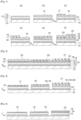
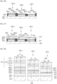
- Figures 1 to 19 illustrate for comparison purposes an embodiment of a method and device which is not part of the state of the art, but which does not solve the problem posed.
- Figures 1 to 6 schematically represent a cross-section through an optoelectronic device at different stages of its manufacture; this device has three groups of pixels.
- TCO transparent conductive layers
- the practical realization of the structure described in this document has proven difficult, for several reasons: First, to be able to guarantee stable primary colors across the substrate (which is typically a silicon wafer with a diameter of 200 mm or 300 mm, with circuits prepared by CMOS technology that are configured to address the pixels), a very good uniformity of the thickness of the optical cavities is required, of the order of 98% to 99%, which is difficult to achieve with deposition methods such as described the state of the art, such as sputtering or chemical vapor deposition (CVD, i.e. Chemical Vapor Deposition, or PECVD, i.e. Plasma Enhanced Chemical Vapor Deposition).
- CVD chemical vapor deposition
- PECVD plasma Enhanced Chemical Vapor Deposition
- the use of the ALD (Atomic Layer Deposition) technique allows to obtain such homogeneity of thickness.
- it can only be applied to a limited number of TCO materials, such as ZnO, AZO (which is a more conductive variant of ZnO), as well as SnO 2 .
- EP 1 672 962 includes a detailed description of a process based on three steps of resin deposition and photolithography, etching and stripping of these three resin layers. With some additions and modifications, this can be translated into a process diagram shown in the figure 1 by images 1(a) to 1(f).
- the starting point is a CMOS type substrate (for example on a silicon wafer), with the metal at the last level to form the pixels, here aluminum coated with a thin layer of TiN as protection against oxidation.
- CMOS substrate 10 coated with a layer of Si 3 N 4 or SiO 2 11 (about 200 nm) and a reflective electrode base layer 12 was taken as the starting point (state (a)); said base electrode comprised an aluminum layer (about 200 nm) sandwiched between a first layer of TiN 13 (about 50 nm), lower, and a second layer of TiN 15 (about 7 nm), upper.
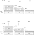
- FIG. 1 shows, for the sake of simplification, only two pixels each belonging to a different group, whereas the Figures 3 to 6 actually show all three groups of pixels.
- a photosensitive resin 22 was deposited and delimited by lithography to fill the space between the pixels and to planarize the surface.
- a white-emitting OLED stack 23 was deposited with a semi-transparent common electrode 24 at the top.
- the thicknesses and positions of the emitters were optimized in order to produce optical cavities for extracting R, G, B primaries with optimum efficiency.
- Three groups of pixels 25,26,27 R,G,B are thus obtained, individually addressable via circuits that are part of the CMOS substrate; these circuits as well as the manner of establishing contact between them and the lower electrode of the pixels 12 are known, are not part of the invention and will not be specified here.
- the final thickness control of the TCO layers is not satisfactory.
- ALD deposition allows to control the thickness of the TCO layers with an accuracy of 1% - 2%, and leads to a very good uniformity on the surface of the substrate, this thickness is reduced during the structuring process.
- the stripping step of the photosensitive resin i.e. the step that leads to the structure shown in the figure 4
- the dry etching process RIE or IBE
- hardens the photosensitive resin which then requires fairly powerful wet stripping in order to remove the resin; this wet stripping also attacks the TCO.
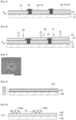
- the edge of the pixel is degraded. Indeed, during the step which leads from state (c) to state (d) of the figure 1 , and during the step leading from state e) of the figure 1 in state f, the TCO deposition occurs partly on the vertical sides of the resin pads photosensitive resin 17 and 19. As the ALD deposition is perfectly conformal, this leads to the formation of vertical TCO walls which partly resist the stripping of the photosensitive resin. This is visible on the figure 7 which represents a scanning electron micrograph: we clearly see rectangular boxes with vertical walls of TCO, while the inside of the boxes is empty; each of these boxes represents a pixel. To remove these vertical walls, an additional wet etching is necessary, which degrades the uniformity of the TCO at the edge of the pixel. This is detrimental to the optical characteristics of the pixels, and more generally to the reliability of the optoelectronic device.
- the characteristic of the OLED pixel is degraded.
- the operating voltage of the OLED deposited on the structure with structured TCO layers
- 1V to 2V which is due to poor injection of the carriers (holes) of the TCO layer into the OLED.
- a stack of at least two layers of different TCOs is used as optical spacer, which are distinguished by their resistance to etching, particularly wet etching: so-called “hard” TCO is more resistant to etching than so-called “soft” TCO.
- Soft TCOs including ZnO and AZO, are very well etched by wet etching followed by dry stripping of the photosensitive resin, for example with O 2 plasma, and this does not impact their thickness. However, they must be protected during the dry etching step to separate the pixels, and during wet stripping of the photosensitive resin. It should be noted that their use as an anode for OLED also leads to an increase in the operating voltage.
- Hard TCOs including SnO 2 , are very resistant to wet etching, and can be etched only by dry etching. In addition, they work well as anodes for OLED stacking, with perfect conservation of the operating voltage compared to an Al/TiN anode.
- a layer of soft TCO is mainly used as optical spacer, but this layer is protected by a thin layer of hard TCO which also provides the interface to the stack of organic layers of the device (OLED layers or photosensitive layers).
- the concept of "soft” and “hard” TCO here refers to a reference wet etching treatment (also called wet “etching” treatment), usually used in microelectronics, namely etching with an aqueous solution of tetramethylammonium hydroxide (no. CAS: 75-59-2 ) at 2.38% by weight; such a product is commercially available, for example from the company ThermoFischer Scientific TM (electronic grade, catalog number 44940. This wet etching is typically carried out at room temperature.
- a “hard” TCO is a TCO that resists significantly better to such a wet etching treatment than a “soft” TCO, this resistance being able to be expressed by the specific etching speed under identical conditions.
- these TCO layers whatever the chemical nature of these TCO layers, they must be selected relative to each other so that this difference in resistance to said reference wet etching treatment is respected.
- the terms “hard” and “soft” do not refer to mechanical characteristics, but only to the resistance to wet etching.
- the invention is not limited to TCOs which are "hard” and “soft” relative to this reference treatment indicated above.
- other etching products and methods can be used, which must however be selected in such a way that the TCOs which are, relative to each other, respectively, “soft” and “hard” under the conditions of the reference treatment, are also, relative to each other, respectively, “soft” and “hard” under the conditions of the chosen etching treatment.
- an advantageous deposition technique is the atomic layer deposition (ALD) technique.
- the hard TCO, the soft TCO and the etching treatment are chosen so that the etching speed of the hard TCO is less than one tenth of the etching speed of the soft TCO, more preferably less than one hundredth, and even more preferably less than one thousandth.
- the etching speed (typically expressed in nm/min) must be adapted to the wet etching process used. If the etching speed is too high, the time between the end of etching and rinsing may induce over-etching that is difficult to control; the etching speed depends on the chemical nature of the TCO, its deposition process and the nature of the etching treatment (in particular the etchant, its concentration and the temperature).
- the "soft" TCOs that can be used to carry out the present invention are ZnO-based TCOs, where ZnO can be doped, for example, with gallium (an oxide called GZO), aluminum (AZO), boron, and/or beryllium.
- GZO gallium
- AZO aluminum
- boron and/or beryllium.
- Another typical "soft" TCO system is indium oxide-based TCO, which can be doped, especially tin; such an oxide known by the acronym ITO (Indium Tin Oxide) is widely used in microelectronics and optoelectronics. ITO cannot be deposited by ALD; indium oxide can be deposited by ALD, but it is a process that is quite difficult to master to guarantee correct stoschiometry.
- the “hard” TCOs that can be used to carry out the present invention are TCOs based on SnO 2 , this SnO 2 being able to be doped, for example with arsenic, fluorine, nitrogen, niobium, phosphorus, antimony.
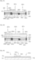
- a substrate 150 is provided, in this case a silicon wafer with circuits structured according to CMOS technology which are configured to address the pixels (or read the voltage or current of the pixels in the case of a sensor); this technology is known as such and will not be explained here.
- This substrate 150 comprises an insulating layer 151 which may in particular be an oxide, a nitride or an oxynitride; Si 3 N 4 is typically used.
- the electrical contacts between the pixels are made via vertical channels arranged through this insulating layer by etching; this is also known.
- This lower electrode 152 may comprise one or more layers. It may for example be made of silver, aluminum, copper, chrome or another metal with high reflectivity, and in this case a single layer may be sufficient. It may also comprise several layers, as described above and as illustrated in the figure 8 . As such, it may comprise, for example, a metal layer 153 (typically aluminum) sandwiched between a first layer 155 (lower) and a second layer 154 (upper).
- a metal layer 153 typically aluminum
- Said silver layer can also be deposited above said second (upper) nitride layer 154 , which gives a TiN / metal / TiN / silver structure, for example TiN / AI / TiN / Ag, listed from bottom to top.
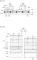
- a first layer 158 of TCO is deposited on this lower reflective electrode 152.
- This TCO layer must be easy to etch by wet etching, it is thus called here a “soft” TCO layer, as opposed to a TCO layer resistant to wet etching, which is called here a “hard” TCO layer.
- a thin layer of “hard” TCO (not shown in these figures), called here a “hard TCO base layer”, which protects the lower electrode 152, can be intercalated between the upper surface of the lower reflective electrode 152 and said first layer of TCO 156 (in “soft” TCO).
- This layer is called here a “hard TCO base layer”, which protects the lower electrode 152.
- soft TCO for example, a layer of AZO, ZnO or ITO can be used, and as “hard” TCO, a layer of SnOz.
- the said thin layer of hard TCO which protects the Lower electrode 152 is visible on the figure 31 (reference number 680) and on the figures 42 and 43, and will be discussed in greater detail in this context. It should be noted that if this layer 680 is present, it will not be part of what is referred to herein as a "bilayer”: a “bilayer”, as that term is used herein, always comprises a first layer (counted from the substrate) of soft TCO and a second layer of hard TCO.
- a structured deposit 158 of photosensitive resin is created on this layer 158 of soft TCO, by photolithographic processes known to those skilled in the art.
- the spacing d, between two neighboring zones 158a, 158b of photosensitive resin corresponds to the spacing between two neighboring pixels.
- the lower electrode 152 is no longer represented with its three layers which are the first (lower) layer of nitride 155, the metal layer 153 and the second (upper) layer of nitride 154, but as a single layer with the numerical reference 152.
- the wet etching of the soft TCO layer 158 is carried out.
- the latter is not removed by said wet etching treatment.
- a structured deposit 182 of photosensitive resin is created on this layer 160 of hard TCO, so that the spacing d 2 between two neighboring zones 162a, 162b of photosensitive resin corresponds to the spacing between two neighboring pixels R,G.
- this structured deposit of photosensitive resin comprises a deposit 162a which is deposited above the structured layer 158 of soft TCO, and another photosensitive deposit 162b which is deposited between two neighboring zones 156a, 156b of soft TCO.
- dry etching is carried out of all the layers 160 of hard TCO, any residues of the soft TCO layer 158 and the reflective electrode 152 to separate the pixels, followed by wet stripping of the photosensitive resin 162.
- Said dry etching is advantageously carried out by RIE (Reactive-ion Etching) or IBE (Ion Beam Etching). A structure is thus obtained, illustrated schematically in FIG. figure 13 .
- a filler element 164 is deposited in the space between two neighboring pixels, for example by photolithographic techniques. This is schematically illustrated in FIG. figure , 14 .
- the OLED stack 170 common to all the pixels, and a semi-reflective upper electrode 166 (also called “top electrode”) which is also common to all the pixels, are deposited on this structured surface.
- a semi-reflective upper electrode 166 also called “top electrode” which is also common to all the pixels.
- Said upper electrode 168 must be semi-reflective and semi-transparent; it forms one of the two reflectors of the optical cavity.
- the optoelectronic device is a detector, it is through it that the light enters the device to be detected by the organic stack which is then in place of the OLED stack.
- An optoelectronic device is thus obtained with two groups of pixels 167a, 167b, each group of pixels having an optical cavity of different optical thickness, designated d R and d G , respectively.
- the optical cavities are formed between the lower electrode 152 of the pixel, which is reflective, and the semi-transparent and semi-reflective electrode 166 at the top.
- the organic stack may be, depending on the destination of the optoelectronic device, an emissive stack of the OLED type or a stack of the organic photodiode type.
- one of the pixels 167a is formed on a TCO layer which is formed from two layers 156,160 of different TCO materials, one 156 soft, the other 160 hard, while the other of the pixels 167b are formed on a TCO layer which is formed only from a single layer 160 of TCO, which is a hard layer.
- the TCO layer may be composed of two chemically different layers 158,180 , it acts in this optoelectronic device as a single optical spacer, and in this function it is here designated by the reference number 157 (visible on the figure 16 ); the fact that it is composed of two chemically different layers 156,180 and of different hardness is motivated solely by practical considerations in relation to the industrial production of optoelectronic devices with high optical efficiency and reliability.
- the refractive index of the two layers of TCO 156,160 is advantageously close to limit the loss of light by multiple reflections.
- This device can be used to realize a display screen with two primary colors, for example red (R) and green (G). It can also be used to realize a light detector responding in two different spectral regions; in this case all the optical paths are reversed and the light-emitting OLED 170 stack will be replaced by a stack of light detector layers.
- the dry etching of the sixth “step” is a directional etching which removes the hard TCO 160 in the space of width d2 between two neighboring zones (see the passage of the figure 12 to the figure 13 ), but which does not remove the vertical walls (flanks) of the hard TCO layer 160, which remain visible on the figure 13 for pixels in the group of those with the thicker optical cavity (thickness d R on the figure 15 ).
- the sides of the hard TCO layer 160 protect the sides of the soft TCO layer 156b on which said hard TCO layer 180 has been deposited, during the dry etching steps (sixth sequence of steps, see figure 13 ) and depositing the filling element 164 (seventh sequence of steps, see figure 14 ).
- an optical spacer is obtained whose TCO 156b, 160 layers have excellent geometric definition with clean and healthy edges.
- This OLED stack comprises a second electrode (top electrode) 166 and one or more encapsulation layers (not shown in the figures) in order to protect the device.
- Said top electrode 166 must be semi-transparent because it is through it that the light emitted by said optoelectronic device leaves the device if it is a light emitter, and it is through it that the light which must be detected by said device enters the device if it is a light detector.
- a first set 171 successively comprises, listed from bottom to top, a hole injection layer (abbreviated HIL, Hole Injection Layer), a hole transport layer (called HTL, Hole Transport Layer), and an electron blocking layer (abbreviated EBL, Electron Blocking Layer).
- a second set 175 of layers comprises the emissive layer(s) (abbreviated EML, Emissive Layer).
- a third set 179 of layers successively comprises a hole blocking layer (abbreviated HBL, Hole Blocking Layer), an electron transport layer (abbreviated ETL, Electron Transport Layer) and an electron injection layer (abbreviated EIL, Electron Injection Layer).
- optical thicknesses d R and d G are chosen so as to form for the pixels of the group G 167b a cavity which makes it possible to extract a maximum of green light in the direction of the normal, and for the pixels of the R 167a group a maximum of red light.
- OLED 170 stack emitting for example a spectrum with a peak in the yellow zone (yellow, abbreviated here Y) of the visible spectrum.
- an OLED 1700 stack with two different emitting layers 1751,1752 namely R and G; such a device is illustrated in FIG. figure 17 .
- the thicknesses d R and d G , as well as the maximum intensity position of the emitting layers 1751,1752, designated respectively z R and z G are to be optimized in order to obtain a maximum emission at normal for the two groups of pixels 1670a,1670b.
- tandem type OLED stack either with two Y cells (illustrated schematically in the figure 18 ), either with an R cell and a G cell (illustrated schematically on the figure 19 ).
- the order of cells G and R can also be reversed (not shown in the figures).
- the thicknesses d R and d G as well as the position of maximum intensity of the emitting layers, z Y1 and z Y2 or z R and z G are to be optimized in order to obtain a maximum emission at the normal for the two groups of pixels.
- tandem type OLED stacks 270 comprise two sets of stacks 2701,2702, separated by a charge generation layer 274 (abbreviated CGL, Charge Generation Layer).
- CGL Charge Generation Layer
- Each of the two sets of stacks 2701,2702 comprises the three sets of layers presented in relation to the figure 16 , namely (from bottom to top): a first set 271,276 of EBL, HTL and HIL layers, a second set 272,278 comprising the emissive layer EML, and a third set 273,279 comprising the EIL, HBL, ETL layers.
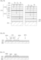
- d R n 156 * e 156 + n 160 * e 160 + n 171 * e 171 + n 175 * e 175 + n 179 * e 179
- d G n 160 * e 160 + n 171 * e 171 + n 175 * e 175 + n 179 * e 179 .
- z Y 0.5 * n 175 * e 175 + n 179 * e 179
- the soft TCO layer 156 must have an optical thickness of 28 nm which corresponds to a physical thickness of 15.5 nm if its optical index is 1.8, knowing that the organic stack 170 and the hard TCO layer 180 are common to all the pixels (and therefore have the same thickness for the pixel 167a and the pixel 167b).
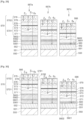
- the first part of the process is analogous to what was previously described for the two-color device, up to and including the fourth sequence of steps, with a set of photolithography masks adapted to a geometry with three different pixel groups.
- an intermediate product is obtained, schematically represented in the figure 20 .
- locations 387a, 367b of the R and G pixel groups it has a structured TCO layer, comprising a first layer 3561 of soft TCO and a first layer 3601 of hard TCO.
- location 387c of the pixel B group there is no soft TCO layer.
- a second layer 3582 of soft TCO is then deposited over the entire structure, as illustrated in the figure 21 .
- a layer of photosensitive resin 332a is deposited at location 367a of the pixel group R, using known photolithographic techniques. This is illustrated in figure 22 .
- a wet etching is carried out to selectively remove said second soft TCO layer 3582 at accessible locations, i.e. not protected by the photosensitive resin 332a.
- the hard TCO layer 3601 protects the first soft TCO layer 3561 at location 367b of the pixel group G.
- the photosensitive resin 332a is removed by a dry etching process, typically with oxygen plasma.
- a second layer 3602 of hard TCO is deposited on the entire structure, to arrive at the structure illustrated in the figure. figure 23 .
- a structured layer 3820 of photosensitive resin is deposited using known photolithographic techniques, as indicated in the figure 24 .
- This photosensitive resin layer 3620a, 3620b, 3620c protects each group of pixels 387a, 367b, 387c during dry etching to separate the pixels.
- This dry etching has the purpose of removing all of the hard TCO layers 3801 and 3802, any soft TCO residues as well as the layer(s) of the reflective electrode 352 at the locations not protected by the photosensitive resin, i.e. at the space between the pixels.
- Said dry etching may be an ion beam etching, as mentioned above.
- the photosensitive resin layer 3620 is then removed by a wet stripping process, thus obtaining the structure illustrated in the figure. figure 25 .
- a filling element 364, for example made of photosensitive resin, is then deposited in the space between two neighboring pixels, as described above; the result is illustrated in the figure 28 .
- the OLED stack 370 is first deposited, then the common electrode 368, which must be semi-transparent. This gives three groups of pixels 367a, 367b, 367c with optical spacers of different optical thickness for each of the three groups of pixels. This device is illustrated in the figure 27 .
- edges (also called flanks) of the TCO layers of the optical spacers of the green pixel groups 367b and red 367a are protected by a layer of hard TCO 3602.
- These sides can be vertical or inclined, which depends on details of the manufacturing process; an example is shown in the figure 40 .
- the upper soft TCO layer 3561 is completely encapsulated by the lower layer of hard TCO 3601, the upper layer of hard TCO 3602 and the sides of said upper layer of hard TCO 3602.
- a sort of hard TCO box is thus created, protecting the internal soft TCO layer.
- the AZO layer has a thickness of 45 nm.
- a device according to the invention can be used to produce a display screen with three primary colors, for example red (R), green (G) and blue (B), in order to produce a color screen of the type known as "full color".
- R red
- G green
- B blue
- OLED stack 470 comprising a set 575 of three different emissive layers 5712,5710,5711 emitting a white spectrum with three peaks in the blue, green and red domain of the spectrum, which is protected by a second semi-transparent electrode (top electrode) 468, and by one or more encapsulation layers (not shown in the figures) in order to protect the device.
- top electrode top electrode
- encapsulation layers not shown in the figures
- the three emitting layers 5712, 5710, 5711 forming the set 575 of organic layers follow one another directly, the first 5712 and the third 5711 (counted from the bottom) being in contact with, respectively, a first set 571 and a third 579 set of organic layers, which have the same functions as the sets 171 and 179 explained above in relation to the figure 16 .
- the result is therefore a device with three groups of pixels 467a, 487b, 467c, each group of pixels being characterized by an optical cavity of different optical thickness, designated d R , d G and d B respectively.
- the cavities are formed between the electrode 452 of the pixel which is reflective, and the semi-transparent and semi-reflective electrode 466 at the top.
- the thicknesses d R , d G and d B as well as the position of maximum intensity of the emitting layer, z w are chosen so as to form for the group of pixels B 467c a cavity which allows to extract, from the light generated by the OLED stack, which can be white light, a maximum of blue light in the direction of the normal, for the group of pixels G 467b a maximum of green light, and for the group of pixels R 467a and a maximum of red light.
- the parameter zw refers to a white emission which results from the emission emanating from the emissive layers of light of blue color 5712, green 5710 and red 5711.
- the position of maximum intensity of the emitting layer designated below by the parameters z B , z G and z R , respectively; these parameters are not shown on the figure 28 so as not to overload it.
- the white emission can also be generated with a combination of a blue emitter and a yellow emitter (not shown in the figures).
- tandem type OLED structure either with a blue light emitting cell B and a yellow light emitting cell Y, or with a light emitting cell B and a red and green light emitting cell RG.
- the first variant is illustrated in the figure 29 , the second on the figure 30 .
- the OLED stack 570 comprises two OLED stacks 5701, 5702 separated by a charge generation layer 574.
- the first stack 5701 (counted from the substrate) has the succession of layers 571 HIL, HTL and EBL which has been described above, then an emissive layer 572 (in this case with the blue emission color), then the succession of layers 573 EIL, ETL, HBL which has already been described above.
- the second stack 5702 has the same functional structure, with the layers the succession of layers 576 HIL, HTL, EBL, an emissive layer 578 of emission color (yellow) different from that of the stack 5701, and the succession of layers 579 EIL, ETL, HBL.
- the semi-reflective and conductive layer 566 common to all the pixels, forms both the upper reflector of the optical cavity and the common upper electrode of the device.
- the tandem cell of the figure 30 has a similar structure, except that in the second OLED stack 5702, the emissive layer 578 is not characterized by a yellow emission color, but is made in the form of two emissive layers 5781,5782 , the first of which emits in red, the second in green.
- the order of cells B and Y or B and RG can also be reversed from what is shown in these figures.
- the thicknesses d R , d G and d B , as well as the position of maximum intensity of the emitting layers, z Y and z B or z RG and z B can be optimized in order to obtain a maximum emission at the normal for the three groups of pixels.
- Z RG 0.5 * n 578 * e 578 + n 579 * e 579
- Z B 0.5 * n 572 * e 572 + n 573 * e 573 + n 574 * e 574 + n 576 * e 576 + n 578 * e 578 + n 579 * e 579
- Tables 1 to 3 show the result of an optimization of the main parameters for different configurations.
- This optimization aims at the best electro-optical performances, in particular a compromise between emission, efficiency and CIE emission spectrum, to determine the key parameters of the device, namely the thicknesses d R , d G and d B and the position of maximum intensity of the emitting layers zw (white light for the geometry of the figure 28 ), or z B and z Y (for the geometry of the figure 29 ), or z B , z G and z R (for the geometry of the figure 30 ).
- This optimization is based on an average value of the optical index of the layers forming the organic stack of 1.7981 at the wavelength of 500 nm, knowing that the optical indices of the different organic layers are very close. It is also based on an optical index at 500 nm of the soft TCO (AZO in this example) of 1.92448293 and of the hard TCO (SnO 2 in this example) of 2.027. References 8, 9, 14 and 15 refer to a first-order emission for the yellow pixel (Y) and to a second-order emission for the blue pixel (B).
- Table 1 Geometry of Figure 28 (single RGB cell) Ref order d S [nm] d G (nm) d B [nm] z G [nm] z B [nm] z X [nm] z G [nm] z B [nm] of has of has of has of has of has 1 1 120 156 178 214 197 233 60 114 45 88 64 121 70 132 2 120 156 178 214 197 233 56 107 45 88 67 127
- Reference 1 three transmitters, to have R,GB Reference 2: two transmitters, namely B, Y.
- the “ord” column indicates the order of optical remission.
- the optoelectronic device has at least three groups of pixels, which are, respectively, R (red), G (green) and B (blue) pixels, the pixels of each group having an emitting layer or (a photosensitive layer in the case where said device is a photodetector), which emits (or detects) in the red, green or blue spectrum, respectively, with an optical thickness d B of between approximately 110 nm and approximately 160 nm, an optical thickness d G of between approximately 160 nm and approximately 220 nm, an optical thickness d R of between approximately 190 nm and approximately 240 nm, a parameter designating the optical position of maximum intensity of white light zw of between approximately 50 nm and approximately 130 nm (preferably between approximately 60 nm and approximately 115 nm), a parameter designating the optical position of maximum intensity of blue light z B comprised between about 40 nm and about 100 nm (preferably
- the optical thickness d B is between about 120 nm and about 155 nm, the optical thickness d is between about 175 nm and about 215 nm, the optical thickness d R is between about 195 nm and about 230 nm, the parameter zw is between about 60 nm and about 115 nm (preferably between about 75 nm and about 100 nm), the parameter z B is between about 45 nm and about 90 nm (preferably between about 55 nm and about 80 nm), the z parameter G is between about 65 nm and about 120 nm (preferably between about 70 nm and about 110 nm) and the z parameter R is between about 70 nm and about 130 nm (preferably between about 80 nm and about 120 nm).
- the optoelectronic device has at least three groups of pixels, which are, respectively, R (red), G (green) and B (blue) pixels, the pixels of each group having a tandem type structure in which the bottom cell has an emitting layer (or a photosensitive layer) which emits (or detects) in the blue spectrum, and the top cell has an emitting layer (or a photosensitive layer) which emits (or detects) in the yellow or red and green spectrum, with an optical thickness d B of between approximately 110 nm and approximately 160 nm (preferably between approximately 120 nm and approximately 155 nm), an optical thickness d G of between approximately 160 nm and approximately 220 nm (preferably between approximately 175 nm and approximately 215 nm), an optical thickness d R of between approximately 190 nm and approximately 240 nm (preferably between approximately 195 nm and about 230 nm), a parameter designating the optical position of maximum
- the optical thickness d is between about 120 nm and about 155 nm
- the optical thickness d G is between about 175 nm and about 215 nm
- the optical thickness d R is between about 195 nm and about 230 nm
- the parameter z B is between about 45 nm and about 85 nm (preferably between about 55 nm and about 80 nm)
- the parameter zy is between about 65 nm and about 130 nm (preferably between about 80 nm and about 115 nm).
- the optoelectronic device has at least three groups of pixels, which are, respectively, R (red), G (green) and B (blue) pixels, the pixels of each group having a tandem type structure in which the bottom cell has an emitting layer (or a photosensitive layer) which emits (or detects) in the blue spectrum, and the top cell has an emitting layer (or a photosensitive layer) which emits (or detects) in the blue spectrum, and the top cell has an emitting layer (or a photosensitive layer) which emits (or detects) in the blue spectrum.
- an optical thickness d B of between about 320 nm and about 390 nm (preferably between about 330 nm and about 375 nm), an optical thickness d G of between about 425 nm and about 500 nm (preferably between about 450 nm and about 490 nm), an optical thickness d R of between about 500 nm and about 575 nm (preferably between about 510 nm and about 565 nm), a parameter designating the optical position of maximum intensity of blue light z B of between about 45 nm and about 100 nm (preferably between about 50 nm and about 95 nm), and a parameter designating the optical position of maximum intensity of yellow (or red and green) light z Y of between about 120 nm and about 390 nm (preferably between about 130 nm and about 375 nm).
- the optical thickness d is comprised between approximately 335 nm and approximately 375 nm), an optical thickness d G comprised between approximately 450 nm and approximately 490 nm), an optical thickness d R comprised between approximately 510 nm and approximately 565 nm), a parameter z B comprised between approximately 55 nm and approximately 90 nm (preferably between approximately 60 nm and approximately 85 nm), and a parameter z Y comprised between approximately 130 nm and approximately 375 nm (preferably between approximately 135 nm and approximately 370 nm).
- the starting point is the intermediate product shown schematically in the figure 33 . It can be obtained by a variant of the process described in relation to the intermediate product shown in the figure 20 using a set of photolithography masks adapted to this new embodiment. We thus obtain after the fourth sequence of steps an intermediate product represented schematically on the figure 33 .
- pixel group G At location 767b of pixel group G it has a structured TCO layer, comprising a first soft TCO layer 7561 and a first hard TCO layer 7601.
- a second layer 7562 of soft TCO is then deposited over the entire structure, as illustrated in the figure 34 .
- a layer of photosensitive resin 762a is deposited at location 767a of the pixel group R, using known photolithographic techniques. This is illustrated in the figure 35 .
- a wet etching is carried out to selectively remove said second soft TCO layer 7562 at accessible locations, i.e. not protected by the photosensitive resin 762a.
- the hard TCO layer 7601 protects the first soft TCO layer 7561 at location 767b of the pixel group G.
- the photosensitive resin layer 762a is removed by a dry etching process, typically with oxygen plasma.
- a second layer of 7802 hard TCO is deposited over the entire structure, to achieve the structure illustrated in the figure. figure 36 .
- a structured layer 7620 of photosensitive resin is deposited using known photolithographic techniques, as indicated in the figure 24 .
- This structured layer of photosensitive resin here comprises three zones 7620a, 7620b, 7620c and thus protects each group of pixels 767a, 767b, 767c during dry etching to separate the pixels.
- this dry etching is to remove at the locations not protected by the photosensitive resin 7620 all of the layers of hard TCO 7601 and 7602, any residues of soft TCO, as well as the layer(s) of the reflective electrode 752 at the locations not protected by the photosensitive resin, i.e. at the space between the pixels.
- Said dry etching may be an ion beam etching, as mentioned above.
- the 7620 photosensitive resin layer is then removed by a wet stripping process, thus obtaining the structure illustrated in the figure. figure 38 .
- a filling element 764 for example made of photosensitive resin, is then deposited in the space between two neighboring pixels, as described above; the result is illustrated in the figure 39 .
- the OLED stack is then deposited, followed by the common electrode, which must be semi-transparent. This gives three groups of pixels with optical spacers of different optical thickness d for each of the three groups of pixels.
- This device is not illustrated by a figure; it is similar to that of the figure 27 , except for the stacking of hard and soft TCO layers on pixel 367a.
- This device can be used to realize a display screen with three primary colors, for example red (R), green (G) and blue (B), to realize a color screen of the type known as "full color", as described above.
- the pixel of the third group 367a has an optical spacer with a height h3 which is greater than the height h2 of the optical spacer of the pixels of the second group 367b.
- the optical spacer of the pixels of the third group 367a is formed by two bilayers, that of the pixels of the second group 367b by a single bilayer.
- the soft TCO layers 3561,3562 are encapsulated by a hard TCO layer 3601.
- FIG. 42 in this variant the optical spacer of the pixels of the third group 367a has a height h2 identical to that of the figure 41 , but there is, for this third group of pixels 367a, only one bilayer; the third group of pixels 367a has, compared to the pixels of the second group 367b, a thickness of the soft TCO layer 7562 which is greater (the relationship h3 > h2 still applies).
- figure 40 represents an extract of such a structure according to the figure 42 : the thickness of the AZO layer (visible in the figure) is 45 nm for the green pixel, and 95 nm for the red pixel (not visible in the figure 40 ).
- appropriate color filters 695a, 695b, 695c are added. This is schematically illustrated in FIG. figure 32 .
- the presence of colored filters does not lead to a significant loss of light intensity because the light emitted by each pixel is not white but colored (which results from the technical effect of optical cavities of different optical lengths).
- the advantage is a better definition and better control of the colors generated by each group of pixels.
- the light emitted by the pixels may have a small second (or even third) order component; in particular, blue light always has a red light component, which corresponds to the second order peak; this higher order component is advantageously absorbed by a filter which only lets through first order light.
- the colored filters 695a, 695b, 695c are placed on a transparent smoothing layer 690, which is an option; it can be made of polymeric material.
- an encapsulation system (not shown in the figures) on the upper electrode 166, 266, 366, 466. It comprises at least one layer, and preferably several layers. It comprises a first layer of alumina, deposited by a conformal deposition technique which is preferably the so-called atomic layer deposition (ALD) technique. It may comprise a second layer of polymer. It may comprise a third layer of alumina, also by ALD. This sequence of alternating layers of alumina and polymer may be repeated one or more times, the last layer preferably being a layer of alumina or titanium oxide.
- ALD atomic layer deposition
- the optoelectronic device according to the invention can be produced in the form of an OLED type light-emitting device; it can be a micro-display.
- the better brightness obtained according to the invention results in reduced electrical consumption and a longer service life.
- Such a high-luminance micro-display can be used for example in augmented reality type glasses or in HUD (Head-Up Display) type devices. It is advantageously produced with at least three groups of pixels of different colors.
- the optoelectronic device can also be produced as a multispectral optical sensor, based on organic photodiodes.
- a sensor transforms the incident light into an electrical signal, which is generated by a photoactive stack of layers, which are preferably organic layers.
- this photoactive stack of layers comprises at least a first material, which is an electron donor, and a second material, which is an electron acceptor.
- a sensor can be made to respond in different areas of the light spectrum, for example in the visible range and/or in the near infrared range.
- Such a sensor is useful in particular in the near infrared spectral range, which typically extends between about 780 nm and about 10 ⁇ m.
- said materials are characterized by the fact that the difference between the energy of the highest occupied level (HOMO - Highest Occupied Molecular Orbital) of said first material and the energy of the lowest unoccupied level (LUMO - Lowest Unoccupied Molecular Orbital) of said second material is less than about 1.6 eV.
- Said first material may for example be a phthalocyanine (such as zinc or iron phthalocyanine) or an aromatic amine (such as N,N,N',N'-Tetrakis(4-methoxyphenyl)benzidine, abbreviated MeO-TPD, CAS No. 122738-21-0) or a polythiophene (such as Poly[2,5-bis(3-tetradecylthiophen-2-yl)thieno[3,2-b]thiophene], abbreviated PBTTT, CAS No. 888491-19-8). These materials may be deposited under vacuum.
- Said second material may be a fullerene, such as C60; these materials may also be deposited under vacuum.
- Such an optoelectronic device can be implemented in the form of a spectrometer (by providing a plurality of groups of pixels, each group of which has an optical cavity of different length), and/or in the form of a camera with spatial and spectral resolution, by providing a plurality of pixels each consisting of a plurality of groups of pixels with an optical cavity of different length.
Landscapes
- Physics & Mathematics (AREA)
- Optics & Photonics (AREA)
- Engineering & Computer Science (AREA)
- Manufacturing & Machinery (AREA)
- Electroluminescent Light Sources (AREA)
- Devices For Indicating Variable Information By Combining Individual Elements (AREA)
Claims (14)
- Optoelektronische Vorrichtung, umfassend ein Substrat (350,450,550,750) und einen Stapel organischer Schichten (370,470), der mindestens eine aktive Schicht umfasst, bei der es sich um eine lichtemittierende Schicht (572,575,578) oder um eine Photodiode handeln kann, die zwischen einer reflektierenden Oberfläche, oder zwischen der Oberfläche einer transparenten Schicht, die direkt auf dieser reflektierenden Oberfläche abgeschieden ist, und einer halbreflektierenden Oberfläche, die in einem gegebenen Abstand gegenüberliegend angeordnet ist und einen optischen Hohlraum mit einer gegebenen optischen Länge d bildet,und wobei die Vorrichtung mindestens drei Gruppen von Pixeln (367a, 367b, 367c;767a,767b,767c) umfasst, von denen jede Gruppe durch einen Hohlraum unterschiedlicher optischer Länge d gekennzeichnet ist, wobei der Hohlraum eine Anzahl von Doppelschichten umfasst, die zwischen dem Substrat und dem Stapel organischer Schichten angeordnet sind, jede Doppelschicht bestehend aus einer ersten transparenten und leitfähigen Schicht (3561,3562,7561,7562) aus einem ersten transparenten und leitfähigen Material, und aus einer zweiten transparenten und leitfähigen Schicht (3601,3602,7601,7602) aus einem zweiten transparenten und leitfähigen Material, das in direktem Kontakt mit der ersten transparenten und leitenden Schicht steht, wobei sich das erste Material vom zweiten Material unterscheidet,und in welcher Vorrichtung:- für eine erste Gruppe (367c,767c) von Pixeln die Anzahl der Doppelschichten Null beträgt,- für eine zweite Gruppe (367b,767b) von Pixeln die Anzahl der Doppelschichten eins beträgt,- für eine dritte Gruppe (367a,767a) von Pixeln die Anzahl der Doppelschichten zwei oder eins beträgt, im letzteren Fall jedoch die erste Schicht der Doppelschicht, die der dritten Gruppe von Pixeln zugeordnet ist, dicker ist als jene der zweiten Gruppe von Pixeln,- für jede weitere Gruppe von Pixeln, sofern vorhanden, sich die Anzahl der Doppelschichten im Vergleich zur vorherigen Gruppe um eins erhöht oder gleich bleibt, jedoch im letzteren Fall ist die erste Schicht der Doppelschicht, die der zusätzlichen Gruppe von Pixeln zugeordnet ist, dicker als die der vorherigen Gruppe von Pixeln,- wobei die Zählung der Gruppen in erste, zweite, dritte und gegebenenfalls usw. in einer Reihenfolge erfolgt, in der der Wert d ansteigt, und wobei in der Vorrichtung für jede dieser Schichten diese erste leitfähige und transparente Schicht, vom Substrat her gezählt, einen geringeren Widerstand gegenüber einer Nassätzbehandlung aufweist als die zweite leitfähige und transparente Schicht, und wobei in der Vorrichtung für jede Gruppe von Pixeln jenseits der ersten zumindest die erste Schicht der am weitesten vom Substrat entfernten Doppelschicht seitlich durch die besagte zweite Schicht der Doppelschicht geschützt ist.
- Vorrichtung nach Anspruch 1, in welcher für jede Gruppe von Pixeln jenseits der ersten die besagte erste Schicht der am weitetsten vom Substrat entfernten Doppelschicht vollständig von der zweiten Schicht der Doppelschicht eingekapselt ist.
- Vorrichtung nach Anspruch 1 oder 2, in welcher für jede Gruppe von Pixeln jenseits der ersten die besagte erste Schicht aller Doppelschichten vollständig von einer Schicht aus einem zweiten transparenten und leitfähigen Material eingekapselt ist.
- Vorrichtung nach einem der Ansprüche 1 bis 3, in welcher die besagte reflektierende Oberfläche mit einer Schicht aus dem zweiten transparenten und leitfähigen Material bedeckt ist.
- Optoelektronische Vorrichtung nach einem der Ansprüche 1 bis 4, in welcher die besagte Nassätzbehandlung eine Behandlung mit einer wässrigen Lösung von Tetramethylammoniumhydroxid mit 2,38 Gew.-% bei Raumtemperatur ist.
- Optoelektronische Vorrichtung nach einem der Ansprüche 1 bis 5, bei der in jeder der Doppelschichten die erste transparente und leitfähige Schicht eine spezifische Ätzgeschwindigkeit V1 aufweist, die mindestens zehnmal höher, vorzugsweise mindestens hundertmal höher und besonders bevorzugt mindestens tausendmal höher ist als die spezifische Ätzgeschwindigkeit V2 der zweiten transparenten Schicht.
- Optoelektronische Vorrichtung nach einem der Ansprüche 1 bis 6, in welcher das erste transparente und leitfähige Material aus der Gruppe ausgewählt ist, die besteht aus: ZnO; dotierten Oxiden auf Basis von ZnO, wobei die Dotierung vorzugsweise Gallium und/oder Aluminium und/oder Bor und/oder Beryllium ist; Indiumoxid; dotierten Oxiden auf der Basis von Indiumoxid, wobei die Dotierung vorzugsweise mit Zinn erfolgt,
und/oder in welcher das zweite transparente und leitfähige Material ausgewählt ist aus der Gruppe bestehend aus: SnO2, dotiertem SnO2, wobei die Dotierung vorzugsweise Arsen und/oder Fluor und/ oder Stickstoff und/oder Niob und/oder Phosphor und/oder Antimon und/oder Aluminium und/oder Titan ist. - Vorrichtung nach einem der Ansprüche 1 bis 7, dadurch gekennzeichnet, dass der Stapel organischer Schichten in direktem Kontakt mit einerseits der besagten reflektierenden Oberfläche oder einer auf der Oberfläche besagter reflektierenden Schicht aufgebrachten transparenten Schicht steht, und/oder andererseits mit der halbreflektierenden Oberfläche.
- Vorrichtung nach einem der Ansprüche 1 bis 8, in welcher der Stapel organischer Schichten eine kontinuierliche Beschichtung über allen Pixeln bildet, und vorzugsweise dadurch, dass er eine halbtransparente und leitfähige Schicht umfasst, die über dem Stapel aus organischen Schichten abgeschieden ist, und die ebenfalls eine durchgehende Beschichtung auf allen Pixeln bildet.
- Optoelektronische Vorrichtung nach einem der Ansprüche 1 bis 9, in welcher das Substrat ein CMOS-Substrat ist, das mit Schaltkreisen ausgestattet ist, die eine individuelle Adressierung oder ein individuelles Lesen von Pixeln ermöglichen.
- Optoelektronische Vorrichtung nach einem der Ansprüche 1 bis 10, in welcher es sich um ein OLED-Mikrodisplay oder einen multispektralen Lichtsensor handelt.
- Herstellungsverfahren für eine optoelektronische Vorrichtung nach einem der Ansprüche 1 bis 11, bei dem:- zunächst eine transparente und leitfähige Schicht (3561) aus einem ersten transparenten und leitfähigen Material auf der ersten reflektierenden Oberfläche oder auf einer auf der ersten reflektierenden Oberfläche abgeschiedenen transparenten und leitfähigen Schicht aus einem zweiten Material abgeschieden wird,- eine erste Maske abgeschieden wird, die eine zweite und eine dritte Gruppe von Pixeln (367b, 387a) abgrenzt und deren Position schützt,- die erste transparente und leitfähige Schicht durch Nassätzen an den Stellen entfernt wird, die nicht durch die erste Maske geschützt sind, wobei diese ungeschützten Stellen die für eine erste Gruppe von Pixeln (376c) vorgesehene Stelle umfassen, und die erste Maske entfernt wird,- eine erste transparente und leitfähige Schicht (3601) aus einem zweiten transparenten Material abgeschieden wird,- eine transparente und leitfähige Schicht (3562) aus einem ersten transparenten und leitfähigen Material abgeschieden wird,- eine zweite Maske (332a) abgeschieden wird, die die dritte Gruppe von Pixeln (367a) begrenzt und ihre Positionen schützt,- die transparente und leitfähige Schicht (3562) aus einem ersten transparenten und leitfähigen Material durch Nassätzen an den Stellen entfernt wird, die nicht durch die zweite Maske geschützt sind, wobei diese ungeschützten Stellen die für die zweite und die erste Gruppe von Pixeln (367b,376c) vorgesehenen Stellen einschließen, und die zweite Maske entfernt wird,- eine zweite transparente und leitfähige Schicht (3602) aus einem zweiten transparenten und leitfähigen Material abgeschieden wird,- eine dritte Maske (3620a, 3620b, 3620c) abgeschieden wird, die die erste, zweite und dritte Gruppe von Pixeln abgrenzt und ihre Position schützt,- die erste und zweite Schicht (3601,3062) aus besagtem zweiten transparenten und leitfähigen Material sowie die reflektierende Schicht (352), und falls vorhanden, die Schicht (680) aus dem zweiten transparenten und leitenden Material, die sie an Stellen bedeckt, die nicht durch die dritte Maske geschützt sind, durch Trockenätzen entfernt werden.
- Herstellungsverfahren für eine optoelektronische Vorrichtung mit drei Gruppen von Pixeln nach Anspruch 12, bei dem das Verfahren durch die folgenden Schritte fortgesetzt wird:- ein Füllelement (364) wird in jedem Zwischenraum zwischen zwei benachbarten Pixeln abgeschieden,- ein Stapel (370) organischer Schichten, der allen Pixeln gemeinsam ist, wird abgeschieden, und über diesem Stapel organischer Schichten wird eine allen Pixeln gemeinsame halbreflektierende Elektrodenschicht (366) abgeschieden.
- Verfahren nach einem der Ansprüche 12 bis 13, bei welchem die Abscheidung der transparenten und leitfähigen Schichten des besagten zweiten transparenten und leitfähigen Materials durch die Atomlagenabscheidungstechnik erfolgt.
Applications Claiming Priority (2)
| Application Number | Priority Date | Filing Date | Title |
|---|---|---|---|
| FR2006988A FR3112243A1 (fr) | 2020-07-02 | 2020-07-02 | Dispositif optoelectronique matriciel en couches minces |
| PCT/IB2021/055950 WO2022003640A1 (fr) | 2020-07-02 | 2021-07-02 | Dispositif optoelectronique et procédé de fabrication pour un dispositif optoelectronique |
Publications (3)
| Publication Number | Publication Date |
|---|---|
| EP4176468A1 EP4176468A1 (de) | 2023-05-10 |
| EP4176468B1 true EP4176468B1 (de) | 2024-11-27 |
| EP4176468C0 EP4176468C0 (de) | 2024-11-27 |
Family
ID=74205898
Family Applications (1)
| Application Number | Title | Priority Date | Filing Date |
|---|---|---|---|
| EP21736747.3A Active EP4176468B1 (de) | 2020-07-02 | 2021-07-02 | Optoelektronische vorrichtung und verfahren zur herstellung einer optoelektronischen vorrichtung |
Country Status (7)
| Country | Link |
|---|---|
| US (1) | US12408509B2 (de) |
| EP (1) | EP4176468B1 (de) |
| JP (1) | JP2023532528A (de) |
| KR (1) | KR20230034376A (de) |
| CN (1) | CN116548092A (de) |
| FR (1) | FR3112243A1 (de) |
| WO (1) | WO2022003640A1 (de) |
Families Citing this family (3)
| Publication number | Priority date | Publication date | Assignee | Title |
|---|---|---|---|---|
| US11980046B2 (en) * | 2020-05-27 | 2024-05-07 | Taiwan Semiconductor Manufacturing Company, Ltd. | Method for forming an isolation structure having multiple thicknesses to mitigate damage to a display device |
| WO2022054150A1 (ja) * | 2020-09-09 | 2022-03-17 | 株式会社 東芝 | 透明電極、透明電極の製造方法、および電子デバイス |
| CN116249415B (zh) * | 2023-05-11 | 2023-08-08 | 南京国兆光电科技有限公司 | 一种有机发光显示器像素电极结构的制备方法 |
Family Cites Families (20)
| Publication number | Priority date | Publication date | Assignee | Title |
|---|---|---|---|---|
| JP2797883B2 (ja) | 1993-03-18 | 1998-09-17 | 株式会社日立製作所 | 多色発光素子とその基板 |
| GB2353400B (en) | 1999-08-20 | 2004-01-14 | Cambridge Display Tech Ltd | Mutiple-wavelength light emitting device and electronic apparatus |
| US6580657B2 (en) * | 2001-01-04 | 2003-06-17 | International Business Machines Corporation | Low-power organic light emitting diode pixel circuit |
| JP4164251B2 (ja) | 2001-10-31 | 2008-10-15 | 東北パイオニア株式会社 | 有機elカラーディスプレイ及びその製造方法 |
| US6861800B2 (en) | 2003-02-18 | 2005-03-01 | Eastman Kodak Company | Tuned microcavity color OLED display |
| KR101079820B1 (ko) | 2003-09-19 | 2011-11-04 | 소니 가부시키가이샤 | 유기 발광 장치 및 그 제조 방법과 표시 장치 |
| US8569948B2 (en) | 2004-12-28 | 2013-10-29 | Samsung Display Co., Ltd. | Electroluminescent devices and methods of making electroluminescent devices including an optical spacer |
| KR100731750B1 (ko) * | 2005-06-23 | 2007-06-22 | 삼성에스디아이 주식회사 | 박막트랜지스터 및 이를 이용한 유기전계발광표시장치의제조방법 |
| JP4450051B2 (ja) | 2007-11-13 | 2010-04-14 | ソニー株式会社 | 表示装置 |
| JP5515237B2 (ja) | 2008-05-14 | 2014-06-11 | セイコーエプソン株式会社 | 発光装置及び電子機器 |
| US20100051973A1 (en) | 2008-08-28 | 2010-03-04 | Seiko Epson Corporation | Light-emitting device, electronic equipment, and process of producing light-emitting device |
| KR101349143B1 (ko) * | 2010-03-30 | 2014-01-08 | 삼성디스플레이 주식회사 | 유기 발광 디스플레이 장치의 제조 방법 |
| JP5617700B2 (ja) | 2011-03-07 | 2014-11-05 | セイコーエプソン株式会社 | 発光装置および発光装置の製造方法 |
| WO2013047457A1 (ja) * | 2011-09-30 | 2013-04-04 | シャープ株式会社 | 表示装置の製造方法および表示装置 |
| JP6286943B2 (ja) | 2013-08-28 | 2018-03-07 | セイコーエプソン株式会社 | 発光装置および電子機器 |
| CN104966723B (zh) * | 2015-07-27 | 2018-03-23 | 京东方科技集团股份有限公司 | 一种有机发光二极管阵列基板、制备方法及显示装置 |
| KR101925510B1 (ko) | 2015-08-14 | 2018-12-05 | 테크니셰 유니베르시테트 드레스덴 | 적외선 전자기 방사선을 검출 및 변환하기 위한 방법 |
| JP2017182892A (ja) | 2016-03-28 | 2017-10-05 | セイコーエプソン株式会社 | 発光素子、発光装置、及び電子機器 |
| JP2019192838A (ja) * | 2018-04-26 | 2019-10-31 | 株式会社Joled | 有機el表示パネル、及び有機el表示パネルの製造方法 |
| FR3091035B1 (fr) * | 2018-12-19 | 2020-12-04 | Commissariat Energie Atomique | PROCEDE DE FABRICATION D’UN PIXEL D’UN MICRO-ECRAN A OLEDs |
-
2020
- 2020-07-02 FR FR2006988A patent/FR3112243A1/fr active Pending
-
2021
- 2021-07-02 JP JP2022581502A patent/JP2023532528A/ja active Pending
- 2021-07-02 WO PCT/IB2021/055950 patent/WO2022003640A1/fr not_active Ceased
- 2021-07-02 CN CN202180057797.7A patent/CN116548092A/zh active Pending
- 2021-07-02 US US18/004,068 patent/US12408509B2/en active Active
- 2021-07-02 KR KR1020237003972A patent/KR20230034376A/ko active Pending
- 2021-07-02 EP EP21736747.3A patent/EP4176468B1/de active Active
Also Published As
| Publication number | Publication date |
|---|---|
| JP2023532528A (ja) | 2023-07-28 |
| US12408509B2 (en) | 2025-09-02 |
| CN116548092A (zh) | 2023-08-04 |
| EP4176468A1 (de) | 2023-05-10 |
| FR3112243A1 (fr) | 2022-01-07 |
| US20230337454A1 (en) | 2023-10-19 |
| EP4176468C0 (de) | 2024-11-27 |
| KR20230034376A (ko) | 2023-03-09 |
| WO2022003640A1 (fr) | 2022-01-06 |
Similar Documents
| Publication | Publication Date | Title |
|---|---|---|
| EP3671849B1 (de) | Erzeugungsverfahren eines pixels für einen mikro-oled-bildschirm | |
| EP4176468B1 (de) | Optoelektronische vorrichtung und verfahren zur herstellung einer optoelektronischen vorrichtung | |
| WO2019193290A1 (fr) | Dispositif électroluminescent à résolution et fiabilité améliorées | |
| WO2008061988A1 (fr) | Electrode de dispositif emissif lumineux de type oled | |
| WO2010000976A2 (fr) | Dispositif d'affichage electronique polychrome a ecran electroluminescent | |
| EP3614439B1 (de) | Pixel eines mikrobildschirms mit organischen elektrolumineszenzdioden | |
| EP1886540B1 (de) | Leuchtschirm zum beleuchten oder anzeigen von bildern mit einer zusammengesetzten transparenten oberen elektrode | |
| FR3020896A1 (fr) | Dispositif matriciel de detection incorporant un maillage metallique dans une couche de detection et procede de fabrication | |
| FR3147928A1 (fr) | Dispositif electroluminescent a matrice active, presentant une resolution amelioree | |
| EP3921871B1 (de) | Elektrolumineszente anzeigevorrichtung | |
| WO2024214034A1 (fr) | Dispositif electroluminescent a matrice active, presentant une resolution amelioree | |
| FR3129523A1 (fr) | Procede de fabrication d’un dispositif optoelectronique | |
| WO2025083579A1 (fr) | Dispositif électroluminescent à matrice active, présentant une résolution améliorée | |
| US20240341157A1 (en) | Multiple distributed bragg reflector pixel array | |
| WO2025202981A1 (fr) | Dispositif électroluminescent à matrice active et haute résolution | |
| FR3157658A1 (fr) | Procédé de fabrication d’un dispositif comprenant une pluralité de pixels | |
| EP3596760A1 (de) | Organische lichtemittierende diode mit durch einschränkung von plasmonen optimierter ausgangsleistung und anzeigevorrichtung mit einer vielzahl solcher dioden | |
| WO2020084250A1 (fr) | Procédé de fabrication d'un pixel d'un micro-écran à oleds | |
| FR3065324A1 (fr) | Pixel d'un micro-ecran a diodes electroluminescentes organiques | |
| FR2962853A1 (fr) | Diode electroluminescente organique et ecran a faible reflectivite. |
Legal Events
| Date | Code | Title | Description |
|---|---|---|---|
| STAA | Information on the status of an ep patent application or granted ep patent |
Free format text: STATUS: UNKNOWN |
|
| STAA | Information on the status of an ep patent application or granted ep patent |
Free format text: STATUS: THE INTERNATIONAL PUBLICATION HAS BEEN MADE |
|
| PUAI | Public reference made under article 153(3) epc to a published international application that has entered the european phase |
Free format text: ORIGINAL CODE: 0009012 |
|
| STAA | Information on the status of an ep patent application or granted ep patent |
Free format text: STATUS: REQUEST FOR EXAMINATION WAS MADE |
|
| 17P | Request for examination filed |
Effective date: 20230202 |
|
| AK | Designated contracting states |
Kind code of ref document: A1 Designated state(s): AL AT BE BG CH CY CZ DE DK EE ES FI FR GB GR HR HU IE IS IT LI LT LU LV MC MK MT NL NO PL PT RO RS SE SI SK SM TR |
|
| DAV | Request for validation of the european patent (deleted) | ||
| DAX | Request for extension of the european patent (deleted) | ||
| REG | Reference to a national code |
Ref country code: DE Ref legal event code: R079 Free format text: PREVIOUS MAIN CLASS: H01L0027320000 Ipc: H10K0039300000 Ref document number: 602021022462 Country of ref document: DE |
|
| GRAP | Despatch of communication of intention to grant a patent |
Free format text: ORIGINAL CODE: EPIDOSNIGR1 |
|
| STAA | Information on the status of an ep patent application or granted ep patent |
Free format text: STATUS: GRANT OF PATENT IS INTENDED |
|
| RIC1 | Information provided on ipc code assigned before grant |
Ipc: H10K 102/10 20230101ALN20240828BHEP Ipc: H10K 71/00 20230101ALI20240828BHEP Ipc: H10K 59/35 20230101ALI20240828BHEP Ipc: H10K 50/852 20230101ALI20240828BHEP Ipc: H10K 39/30 20230101AFI20240828BHEP |
|
| RIC1 | Information provided on ipc code assigned before grant |
Ipc: H10K 102/10 20230101ALN20240905BHEP Ipc: H10K 71/00 20230101ALI20240905BHEP Ipc: H10K 59/35 20230101ALI20240905BHEP Ipc: H10K 50/852 20230101ALI20240905BHEP Ipc: H10K 39/30 20230101AFI20240905BHEP |
|
| INTG | Intention to grant announced |
Effective date: 20240916 |
|
| GRAS | Grant fee paid |
Free format text: ORIGINAL CODE: EPIDOSNIGR3 |
|
| GRAA | (expected) grant |
Free format text: ORIGINAL CODE: 0009210 |
|
| STAA | Information on the status of an ep patent application or granted ep patent |
Free format text: STATUS: THE PATENT HAS BEEN GRANTED |
|
| RAP3 | Party data changed (applicant data changed or rights of an application transferred) |
Owner name: COMMISSARIAT A L'ENERGIE ATOMIQUE ET AUX ENERGIESALTERNATIVES Owner name: MICROOLED |
|
| AK | Designated contracting states |
Kind code of ref document: B1 Designated state(s): AL AT BE BG CH CY CZ DE DK EE ES FI FR GB GR HR HU IE IS IT LI LT LU LV MC MK MT NL NO PL PT RO RS SE SI SK SM TR |
|
| REG | Reference to a national code |
Ref country code: GB Ref legal event code: FG4D Free format text: NOT ENGLISH |
|
| REG | Reference to a national code |
Ref country code: CH Ref legal event code: EP |
|
| REG | Reference to a national code |
Ref country code: DE Ref legal event code: R096 Ref document number: 602021022462 Country of ref document: DE |
|
| REG | Reference to a national code |
Ref country code: IE Ref legal event code: FG4D Free format text: LANGUAGE OF EP DOCUMENT: FRENCH |
|
| U01 | Request for unitary effect filed |
Effective date: 20241128 |
|
| U07 | Unitary effect registered |
Designated state(s): AT BE BG DE DK EE FI FR IT LT LU LV MT NL PT RO SE SI Effective date: 20241209 |
|
| PG25 | Lapsed in a contracting state [announced via postgrant information from national office to epo] |
Ref country code: IS Free format text: LAPSE BECAUSE OF FAILURE TO SUBMIT A TRANSLATION OF THE DESCRIPTION OR TO PAY THE FEE WITHIN THE PRESCRIBED TIME-LIMIT Effective date: 20250327 Ref country code: HR Free format text: LAPSE BECAUSE OF FAILURE TO SUBMIT A TRANSLATION OF THE DESCRIPTION OR TO PAY THE FEE WITHIN THE PRESCRIBED TIME-LIMIT Effective date: 20241127 |
|
| PG25 | Lapsed in a contracting state [announced via postgrant information from national office to epo] |
Ref country code: ES Free format text: LAPSE BECAUSE OF FAILURE TO SUBMIT A TRANSLATION OF THE DESCRIPTION OR TO PAY THE FEE WITHIN THE PRESCRIBED TIME-LIMIT Effective date: 20241127 |
|
| PG25 | Lapsed in a contracting state [announced via postgrant information from national office to epo] |
Ref country code: NO Free format text: LAPSE BECAUSE OF FAILURE TO SUBMIT A TRANSLATION OF THE DESCRIPTION OR TO PAY THE FEE WITHIN THE PRESCRIBED TIME-LIMIT Effective date: 20250227 |
|
| PG25 | Lapsed in a contracting state [announced via postgrant information from national office to epo] |
Ref country code: GR Free format text: LAPSE BECAUSE OF FAILURE TO SUBMIT A TRANSLATION OF THE DESCRIPTION OR TO PAY THE FEE WITHIN THE PRESCRIBED TIME-LIMIT Effective date: 20250228 |
|
| PG25 | Lapsed in a contracting state [announced via postgrant information from national office to epo] |
Ref country code: PL Free format text: LAPSE BECAUSE OF FAILURE TO SUBMIT A TRANSLATION OF THE DESCRIPTION OR TO PAY THE FEE WITHIN THE PRESCRIBED TIME-LIMIT Effective date: 20241127 |
|
| PG25 | Lapsed in a contracting state [announced via postgrant information from national office to epo] |
Ref country code: RS Free format text: LAPSE BECAUSE OF FAILURE TO SUBMIT A TRANSLATION OF THE DESCRIPTION OR TO PAY THE FEE WITHIN THE PRESCRIBED TIME-LIMIT Effective date: 20250227 |
|
| PG25 | Lapsed in a contracting state [announced via postgrant information from national office to epo] |
Ref country code: SM Free format text: LAPSE BECAUSE OF FAILURE TO SUBMIT A TRANSLATION OF THE DESCRIPTION OR TO PAY THE FEE WITHIN THE PRESCRIBED TIME-LIMIT Effective date: 20241127 |
|
| PG25 | Lapsed in a contracting state [announced via postgrant information from national office to epo] |
Ref country code: SK Free format text: LAPSE BECAUSE OF FAILURE TO SUBMIT A TRANSLATION OF THE DESCRIPTION OR TO PAY THE FEE WITHIN THE PRESCRIBED TIME-LIMIT Effective date: 20241127 |
|
| PG25 | Lapsed in a contracting state [announced via postgrant information from national office to epo] |
Ref country code: CZ Free format text: LAPSE BECAUSE OF FAILURE TO SUBMIT A TRANSLATION OF THE DESCRIPTION OR TO PAY THE FEE WITHIN THE PRESCRIBED TIME-LIMIT Effective date: 20241127 |
|
| U20 | Renewal fee for the european patent with unitary effect paid |
Year of fee payment: 5 Effective date: 20250731 |
|
| PLBE | No opposition filed within time limit |
Free format text: ORIGINAL CODE: 0009261 |
|
| STAA | Information on the status of an ep patent application or granted ep patent |
Free format text: STATUS: NO OPPOSITION FILED WITHIN TIME LIMIT |
|
| 26N | No opposition filed |
Effective date: 20250828 |