EP1884150B1 - Verbesserte leiterplattenbaugruppe - Google Patents
Verbesserte leiterplattenbaugruppe Download PDFInfo
- Publication number
- EP1884150B1 EP1884150B1 EP06727051A EP06727051A EP1884150B1 EP 1884150 B1 EP1884150 B1 EP 1884150B1 EP 06727051 A EP06727051 A EP 06727051A EP 06727051 A EP06727051 A EP 06727051A EP 1884150 B1 EP1884150 B1 EP 1884150B1
- Authority
- EP
- European Patent Office
- Prior art keywords
- pcb
- pcb assembly
- aperture
- slug
- shielding
- Prior art date
- Legal status (The legal status is an assumption and is not a legal conclusion. Google has not performed a legal analysis and makes no representation as to the accuracy of the status listed.)
- Expired - Lifetime
Links
Images



Classifications
-
- H—ELECTRICITY
- H05—ELECTRIC TECHNIQUES NOT OTHERWISE PROVIDED FOR
- H05K—PRINTED CIRCUITS; CASINGS OR CONSTRUCTIONAL DETAILS OF ELECTRIC APPARATUS; MANUFACTURE OF ASSEMBLAGES OF ELECTRICAL COMPONENTS
- H05K3/00—Apparatus or processes for manufacturing printed circuits
- H05K3/30—Assembling printed circuits with electric components, e.g. with resistors
- H05K3/301—Assembling printed circuits with electric components, e.g. with resistors by means of a mounting structure
-
- H—ELECTRICITY
- H05—ELECTRIC TECHNIQUES NOT OTHERWISE PROVIDED FOR
- H05K—PRINTED CIRCUITS; CASINGS OR CONSTRUCTIONAL DETAILS OF ELECTRIC APPARATUS; MANUFACTURE OF ASSEMBLAGES OF ELECTRICAL COMPONENTS
- H05K3/00—Apparatus or processes for manufacturing printed circuits
- H05K3/30—Assembling printed circuits with electric components, e.g. with resistors
- H05K3/32—Assembling printed circuits with electric components, e.g. with resistors electrically connecting electric components or wires to printed circuits
- H05K3/325—Assembling printed circuits with electric components, e.g. with resistors electrically connecting electric components or wires to printed circuits by abutting or pinching; Mechanical auxiliary parts therefor
-
- H—ELECTRICITY
- H05—ELECTRIC TECHNIQUES NOT OTHERWISE PROVIDED FOR
- H05K—PRINTED CIRCUITS; CASINGS OR CONSTRUCTIONAL DETAILS OF ELECTRIC APPARATUS; MANUFACTURE OF ASSEMBLAGES OF ELECTRICAL COMPONENTS
- H05K9/00—Screening of apparatus or components against electric or magnetic fields
- H05K9/0007—Casings
- H05K9/002—Casings with localised screening
- H05K9/0022—Casings with localised screening of components mounted on printed circuit boards [PCB]
- H05K9/0024—Shield cases mounted on a PCB, e.g. cans or caps or conformal shields
- H05K9/0032—Shield cases mounted on a PCB, e.g. cans or caps or conformal shields having multiple parts, e.g. frames mating with lids
- H05K9/0035—Shield cases mounted on a PCB, e.g. cans or caps or conformal shields having multiple parts, e.g. frames mating with lids with retainers mounted beforehand on the PCB, e.g. clips
-
- H—ELECTRICITY
- H05—ELECTRIC TECHNIQUES NOT OTHERWISE PROVIDED FOR
- H05K—PRINTED CIRCUITS; CASINGS OR CONSTRUCTIONAL DETAILS OF ELECTRIC APPARATUS; MANUFACTURE OF ASSEMBLAGES OF ELECTRICAL COMPONENTS
- H05K2201/00—Indexing scheme relating to printed circuits covered by H05K1/00
- H05K2201/03—Conductive materials
- H05K2201/0332—Structure of the conductor
- H05K2201/0388—Other aspects of conductors
- H05K2201/0397—Tab
-
- H—ELECTRICITY
- H05—ELECTRIC TECHNIQUES NOT OTHERWISE PROVIDED FOR
- H05K—PRINTED CIRCUITS; CASINGS OR CONSTRUCTIONAL DETAILS OF ELECTRIC APPARATUS; MANUFACTURE OF ASSEMBLAGES OF ELECTRICAL COMPONENTS
- H05K2201/00—Indexing scheme relating to printed circuits covered by H05K1/00
- H05K2201/10—Details of components or other objects attached to or integrated in a printed circuit board
- H05K2201/10227—Other objects, e.g. metallic pieces
- H05K2201/10371—Shields or metal cases
-
- H—ELECTRICITY
- H05—ELECTRIC TECHNIQUES NOT OTHERWISE PROVIDED FOR
- H05K—PRINTED CIRCUITS; CASINGS OR CONSTRUCTIONAL DETAILS OF ELECTRIC APPARATUS; MANUFACTURE OF ASSEMBLAGES OF ELECTRICAL COMPONENTS
- H05K2201/00—Indexing scheme relating to printed circuits covered by H05K1/00
- H05K2201/10—Details of components or other objects attached to or integrated in a printed circuit board
- H05K2201/10431—Details of mounted components
- H05K2201/10507—Involving several components
- H05K2201/1053—Mounted components directly electrically connected to each other, i.e. not via the PCB
-
- H—ELECTRICITY
- H05—ELECTRIC TECHNIQUES NOT OTHERWISE PROVIDED FOR
- H05K—PRINTED CIRCUITS; CASINGS OR CONSTRUCTIONAL DETAILS OF ELECTRIC APPARATUS; MANUFACTURE OF ASSEMBLAGES OF ELECTRICAL COMPONENTS
- H05K2201/00—Indexing scheme relating to printed circuits covered by H05K1/00
- H05K2201/10—Details of components or other objects attached to or integrated in a printed circuit board
- H05K2201/10613—Details of electrical connections of non-printed components, e.g. special leads
- H05K2201/10621—Components characterised by their electrical contacts
- H05K2201/10636—Leadless chip, e.g. chip capacitor or resistor
-
- H—ELECTRICITY
- H05—ELECTRIC TECHNIQUES NOT OTHERWISE PROVIDED FOR
- H05K—PRINTED CIRCUITS; CASINGS OR CONSTRUCTIONAL DETAILS OF ELECTRIC APPARATUS; MANUFACTURE OF ASSEMBLAGES OF ELECTRICAL COMPONENTS
- H05K2201/00—Indexing scheme relating to printed circuits covered by H05K1/00
- H05K2201/10—Details of components or other objects attached to or integrated in a printed circuit board
- H05K2201/10613—Details of electrical connections of non-printed components, e.g. special leads
- H05K2201/10954—Other details of electrical connections
- H05K2201/10962—Component not directly connected to the PCB
-
- Y—GENERAL TAGGING OF NEW TECHNOLOGICAL DEVELOPMENTS; GENERAL TAGGING OF CROSS-SECTIONAL TECHNOLOGIES SPANNING OVER SEVERAL SECTIONS OF THE IPC; TECHNICAL SUBJECTS COVERED BY FORMER USPC CROSS-REFERENCE ART COLLECTIONS [XRACs] AND DIGESTS
- Y02—TECHNOLOGIES OR APPLICATIONS FOR MITIGATION OR ADAPTATION AGAINST CLIMATE CHANGE
- Y02P—CLIMATE CHANGE MITIGATION TECHNOLOGIES IN THE PRODUCTION OR PROCESSING OF GOODS
- Y02P70/00—Climate change mitigation technologies in the production process for final industrial or consumer products
- Y02P70/50—Manufacturing or production processes characterised by the final manufactured product
Definitions
- the present invention relates to printed circuit board (PCB) assemblies and particularly, but not exclusively, to a system for shielding components from radio frequency interference (RFI) and more particularly to a system for shielding surface mounted devices (SMD).
- PCB printed circuit board
- RFID radio frequency interference
- SMD surface mounted devices
- the present invention provides a printed circuit board (PCB) assembly according to the appended claim 1.
- PCB printed circuit board
- the or each barb may be provided on the RF shielding can so as to be engageable with a slug on the printed circuit board, and in this way a gripping engagement between the circuit board and the RF shielding can is achieved which retains the printed circuit board and RF shielding can in position relative to one another.
- This use of a barb provides a simple and relatively inexpensive means for securing a printed circuit board and RF shielding can together.
- the present invention also provides a printed circuit board assembly comprising further novel and advantageous features as recited in any of the appended dependent claims 2 to 21.
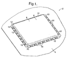
- PCB assembly 2 according to the present invention is shown in Figure 1 of the accompanying drawings as comprising a printed circuit board (PCB) 4 to which is mounted a RF shielding can 6.
- the shielding can typically encloses one or more electrical components (not shown).
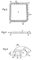
- the RF shielding can 4 comprises a square upper surface 8 from the edges of which four side portions 10 are downwardly bent through 90°. The five surfaces of a box are thereby formed. It will also be understood from the accompanying drawings that a flange element 12 is bent outwardly through 90° from each side surface 10 so as to provide an abutment surface 14 (see Figure 3 ) with the PCB 4.
- the RF shielding can 6 is manufactured from stainless steel, however it will be understood that other materials and alternative shapes for the shielding can 6 may be used.
- the shielding can 6 is secured to the PCB 4 by securing means comprising a plurality of slugs 16 which are attached to the PCB 4 and extend upwardly from a surface thereof through a plurality of apertures provided in each flange element 12 of the shielding can 6.
- securing means comprising a plurality of slugs 16 which are attached to the PCB 4 and extend upwardly from a surface thereof through a plurality of apertures provided in each flange element 12 of the shielding can 6.
- each slug 16 extends into an aperture provided in a flange element 12 and thereby engages with the flange element 12 in such a way as to prevent a ready return of the slug 16 from the respective aperture.
- Each slug 16 is provided as a rectangular block, however alternative shapes will be apparent to a reader skilled in the art.
- the slugs 16 should be of a relatively simple and symmetrical shape so that they may be manufactured relatively inexpensively and be conveniently positioned in large quantities on the PCB 4 by conventional pick-and-place manufacturing techniques. Each slug 16 may be attached to the PCB 4 with solder 18 or other suitable adhesive.
- each slug 16 are positioned so as to align with the apertures 20 (see Figure 2 in particular) provided along each flange element 12.
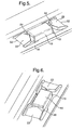
- the relative geometry of the slugs 16 and the RF shielding can 6 is such that, as the flange elements 12 are brought into abutment with the PCB 4 during assembly, each slug 16 projects from one side of an aperture 20 to the other side thereof. In so doing, two barbs 22 extending from opposite perimeter edges of each aperture 20 are deflected by each slug 16.
- each aperture 20 has a generally rectangular shape and the two barbs 22 extend from the shorter sides of the rectangle towards the centre of the aperture 20.
- the barbs 22 each terminate in a point 24 which, in use, tends to penetrate the material of a slug 16 or the solder 18 attaching the slug 16 to the PCB 4. It will be appreciated that the distance between the two points 24 associated with an aperture 20 is less than the associated dimension of the slug 16 to be located in the aperture 20 so that, when the slug 16 is pressed through the aperture 20, the slug 16 abuts each opposing barb 22 and upwardly deflects each barb 22 (see Figure 8 ).
- each barb 22 As a slug 16 is pressed through an aperture 20 and bends each barb 22 upwardly from the plane of the respective flange element 12, the point 24 of each barb 22 penetrates the slug and/or solder and thereby prevents a ready return of the slug 16 from the aperture 20.
- a firm securing of the RF shielding can 6 to the PCB 4 is achieved as a consequence.
- the shielding can 6 is stamped and bent from a sheet of stainless steel material having a thickness of 0.2 mm.
- the distance 26 between the points 24 is 1.2 mm and the width 28 of each aperture 20 is 1.2 mm. It will be understood that each barb 22 is conveniently formed from the material of the RF shielding can 6 when each aperture 20 is stamped therein.
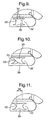
- FIG. 9 An example of different arrangements for the barbs is shown in Figures 9 to 11 of the accompanying drawings.
- Figure 9 an aperture 30 is shown with barbs 32 similar to the barbs 22 of Figures 1 to 8 but without the point 24.
- the opposing edges 34 of the barbs 32 are ideally chamfered or otherwise sharpened so as to increase the tendency for penetration into the material of the slug or the solder attaching the slug to the PCB.
- Figure 10 the arrangement of Figures 1 to 8 has been modified with the addition of a third barb 36 extending laterally towards the centre of the aperture 20 from a third side of the rectangular aperture 20.
- the third barb 36 has a shorter length than the first and second barbs 22 but, like the first and second barbs 22, has a point 24 which assists in penetrating a slug or the solder associated therewith.
- Figure 11 which is identical to that of Figure 10 other than that the distance 26 between the points 24 of the first and second barbs 22 has been increased from 1.2 mm to 1.3 mm.
- a fourth barb may also be provided so that a barb extends from each straight side of a square or rectangular aperture. Each barb will be positioned so as to be deflected when a slug 16 is inserted through the associated aperture.
- the pressing of the flange elements 12 over a plurality of slugs 16 provided on a PCB 4 is assisted by means of an assembly tool 40 such as that shown in Figures 12 to 14 .
- the assembly tool 40 comprises a block of material (for example, stainless steel) having a recess 42 defined in a bottom surface thereof.
- the recess 42 is sized and shaped, and has sufficient depth, to receive the upper surface 8 and side surfaces 10 of the RF shielding can 6 to be secured to the PCB 4.
- a perimeter wall 44 extending around the recess 42 has the same or similar plan footprint as the combined flange elements 12 of the shielding can 6.
- the lower surface 46 of the perimeter wall 44 is engageable with an upper surface 48 (see Figure 3 ) of the shielding can flange elements 12 so that the flange elements 12 may be evenly pressed along their length in a downward direction towards the PCB 4.
- the lower surface 46 of the perimeter wall 44 is provided with a plurality of recesses 50 which, during manufacture of the PCB assembly 2, each receive a slug 16 and the barbs 22, 36 associated with the aperture through which said slug projects.
- Each recess 50 may be sized and shaped so that its perimeter locates along a fold line 52 (see Figure 5 ) associated with each barb so as to encourage a particular bending of each barb.
- the assembly tool 40 is provided with a slot 54 in each of its four sides which facilitates the gripping of the tool 40 either by hand or by automated machinery.
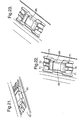
- Figs 15 to 20 show an alternative embodiment of the invention wherein the flange 12 includes one or more tabs 60 in addition to the barbs, for contact with the slugs 65. More specifically, a tab 60 is disposed in each of the four corner regions of the apertures 20.
- the barbs 61 of this embodiment are narrower than the barbs 22 discussed above, thus allowing space for the tabs 60 either side of the barbs 61.
- the barbs 61 and tabs 60 Prior to engagement of the shielding can 6 with the PCB 4, the barbs 61 and tabs 60 lie in the plane of the flange 12, and as a result of engaging with the slugs 65 the barbs and tabs are bent upwardly out of the plane of the flange 12.
- each tab 60 comprises a proximal tab portion 62 connected to the flange 12, a medial tab portion 63 adjoining the proximal tab portion 62 and angled downwardly therefrom, and a distal tab portion 64 connected to the medial tab portion 63 and parallel to the proximal tab member 62, each tab 60 thereby comprising a stepped tongue which can resiliently engage under at least part of the slug 65.
- the stepped profile of the tab 60 adds to its resilience, which resilience allows the tabs 60 to be moved from their positions shown in Figs 15 to 17 , abutting the end faces of the slug 65, to their positions shown in Figs 18 to 20 , engaging underneath the slug 65.
- the tabs 60 enhance the securing of the RF shielding can to the PCB 4.
- the barbs 61 can engage into solder 66 which is used to hold the slugs 65 to the PCB 4, in this case, the soldering 66 being particularly localised so as not to prevent the tabs 60 moving to their engaged position under the slug 65.
- the flange 12 includes a ridge 67 at the longitudinal edges of each aperture 20, which ridge 67 protrudes slightly into the aperture 20.
- the ridges 67 can act to prevent lateral motion of the flange 12 relative to the PCB 4, to a given tolerance, and to guide the shielding can 6 as it is brought into position over the slugs 65.
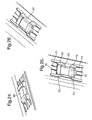
- Figs 21 to 26 show another embodiment where, in contrast to the previous embodiment, the flange 12 includes barbs 71 in each of the four corner regions of the apertures 20 and a tab 70 situated at each end of the aperture, located in between the barbs 71.
- the barbs 71 and tabs 70 slant upwardly away from the plane of the flange 12, when the shielding can has initially been pressed over the slugs.
- the tabs 70 again each comprise a stepped tongue for engaging resiliently underneath the slug 65.
- the slug 65 is connected to the PCB 4 by soldering 72 at each of the four corners of the slug 65, sufficient space being left between the solder joints 72 to allow the tabs 70 to move into their engaged position, which is shown in Figs 24 to 26 .
- the slugs 65 comprise readily available components for use with PCBs, such as resistors. Such slugs can be used with any of the embodiments disclosed herein.
- the use of readily available components avoids the need for the design and development of a custom-built slug thereby reducing costs. It is possible to use a zero-ohm resistor, these being particularly cheap compared to other resistance values. As its name suggests, a zero-ohm resistor has a very small resistance and can be seen as a conductor.
- the electrical properties of the component as such are not critical; it is the size, shape and to some extent, physical strength of the component which determines its usability.
- the component forming the slug is electrically connected to the shielding can 6, and thus contributes to the efficacy of the shielding effect, by having a grounding effect on the shielding can 6, especially when a zero-ohm resistor is used.
- Other resistance values such as 50 ohms and 75 ohms can also be used.
- the pressing of the flanges 12 over the slugs 65 is assisted by means of the assembly tool 40 mentioned above, with suitable means added for pressing the tabs 60,70 downwardly to engage or clip under the slugs 65, whilst avoiding pressing down the barbs 61,71.
- suitable means can comprise abutments (not shown in the drawings) provided in the recesses 50 to line up with the tabs and avoid the barbs.
- a shielding can may be provided with barbs which engage directly with an electrical component to be shielded (or with the solder attaching said component to the PCB).
Landscapes
- Engineering & Computer Science (AREA)
- Microelectronics & Electronic Packaging (AREA)
- Manufacturing & Machinery (AREA)
- Metallurgy (AREA)
- Shielding Devices Or Components To Electric Or Magnetic Fields (AREA)
- Structure Of Printed Boards (AREA)
- Mounting Of Printed Circuit Boards And The Like (AREA)
Claims (21)
- Leiterplattenanordnung (2), die eine Leiterplatte (4) und einen daran angebrachten Hochfrequenz(HF)-Abschirmbecher (6) umfasst, wobei die Leiterplatte (4) und der HF-Abschirmbecher (6) mit Befestigungseinrichtungen aneinander befestigt sind, die eine Vielzahl von Blöcken (16) umfassen, die sich von einer Oberfläche der Leiterplatte (4) nach oben erstrecken, und jeder Block in einer Öffnung (20) aufgenommen werden kann, die in dem Material des HF-Abschirmbechers (6) vorhanden ist, dadurch gekennzeichnet, dass wenigstens ein Widerhaken (22) am Umfang jeder Öffnung (20) vorhanden ist und der Widerhaken (22) so ausgeführt ist, dass er sich biegt und in den Block (16) eindringt, der in jeder Öffnung (20) aufgenommen ist.
- Leiterplattenanordnung (2) nach Anspruch 1, wobei sich ein zweiter Widerhaken (22) vom Umfang der Öffnung aus erstreckt.
- Leiterplattenanordnung (2) nach Anspruch 2, wobei sich der erste und der zweite Widerhaken (22) an einander gegenüberliegenden Seiten jeder Öffnung (20) befinden und sich aufeinander zu erstrecken.
- Leiterplattenanordnung (2) nach einem der Ansprüche 1 bis 3, wobei vier Widerhaken (22) vorhanden sind, von denen sich jeder in einem Eckenbereich der Öffnung (20) befindet.
- Leiterplattenanordnung (2) nach einem der vorangehenden Ansprüche, wobei der oder jeder Widerhaken (22) einen Abschnitt aus Material umfasst, der in einer Spitze endet.
- Leiterplattenanordnung (2) nach einem der vorangehenden Ansprüche, wobei der oder jeder Widerhaken (22) einen Abschnitt aus Material umfasst, der federnd flexibel ist.
- Leiterplattenanordnung (2) nach Anspruch 6, wobei der Widerhaken (22) nicht über seine Elastizitätsgrenze hinaus gebogen wird, wenn der HF-Abschirmbecher (6) an der Leiterplatte (4) befestigt wird.
- Leiterplattenanordnung (2) nach einem der vorangehenden Ansprüche, wobei sich der oder jeder Widerhaken (22) von dem HF-Abschirmbecher (6) aus erstreckt und in Haftmittel eindringt, mit dem ein Block (16) an der Leiterplatte (4) befestigt ist.
- Leiterplattenanordnung (2) nach Anspruch 8, wobei das Haftmittel Lötmetall (18) ist.
- Leiterplattenanordnung (2) nach einem der vorangehenden Ansprüche, wobei der Block (16) ein elektrisches Bauteil, wie beispielsweise einen Widerstand, umfasst.
- Leiterplattenanordnung (2) nach Anspruch 10, wobei der Widerstand (16) ein Null-Ohm-Widerstand ist.
- Leiterplattenanordnung (2) nach einem der vorangehenden Ansprüche, wobei die Befestigungseinrichtung des Weiteren wenigstens eine Zunge (60) umfasst.
- Leiterplattenanordnung (2) nach Anspruch 12, wobei sich die Zunge (60) vom Umfang einer Öffnung (20) aus erstreckt, die in dem Material des HF-Abschirmbechers vorhanden ist.
- Leiterplattenanordnung (2) nach Anspruch 13, wobei sich eine zweite Zunge (60) von dem Umfang der Öffnung (20) aus erstreckt.
- Leiterplattenanordnung (2) nach Anspruch 14, wobei sich die zwei Zungen (60) an einander gegenüberliegenden Seiten der Öffnung (20) befinden und sich aufeinander zu erstrecken.
- Leiterplattenanordnung (2) nach einem der Ansprüche 12 bis 15, wobei die oder jede Zunge (60) einen Abschnitt aus Material umfasst, der elastisch flexibel ist.
- Leiterplattenanordnung (2) nach Anspruch 16, wobei die Zunge (60) nicht über ihre Elastizitätsgrenze hinaus gebogen wird.
- Leiterplattenanordnung (2) nach einem der Ansprüche 12 bis 17, wobei die oder jede Zunge (60) unter wenigstens einen Teil eines Blocks (16) eingreift.
- Leiterplattenanordnung (2) nach einem der Ansprüche 12 bis 18, wobei sich der oder jeder Widerhaken (22) zwischen paarigen Zungen (60) befindet.
- Leiterplattenanordnung (2) nach einem der Ansprüche 12 bis 18, wobei sich die oder jede Zunge (60) zwischen paarigen Widerhaken (22) befindet.
- Leiterplattenanordnung (2) nach einem der Ansprüche 12 bis 20, wobei die jeweiligen Größen des Blocks (16) und der Öffnung (20) so sind, dass, wenn der Block (16) in der Öffnung (20) aufgenommen wird, wenigstens eine Zunge (60) federnd gebogen und dann unter den Block (16) in Eingriff geschoben wird.
Applications Claiming Priority (2)
| Application Number | Priority Date | Filing Date | Title |
|---|---|---|---|
| GB0510925A GB2426633A (en) | 2005-05-27 | 2005-05-27 | Component securing means |
| PCT/GB2006/001688 WO2006125947A2 (en) | 2005-05-27 | 2006-05-09 | Improved printed circuit board assembly |
Publications (2)
| Publication Number | Publication Date |
|---|---|
| EP1884150A2 EP1884150A2 (de) | 2008-02-06 |
| EP1884150B1 true EP1884150B1 (de) | 2009-07-22 |
Family
ID=34834798
Family Applications (1)
| Application Number | Title | Priority Date | Filing Date |
|---|---|---|---|
| EP06727051A Expired - Lifetime EP1884150B1 (de) | 2005-05-27 | 2006-05-09 | Verbesserte leiterplattenbaugruppe |
Country Status (5)
| Country | Link |
|---|---|
| EP (1) | EP1884150B1 (de) |
| AT (1) | ATE437559T1 (de) |
| DE (1) | DE602006007985D1 (de) |
| GB (1) | GB2426633A (de) |
| WO (1) | WO2006125947A2 (de) |
Families Citing this family (3)
| Publication number | Priority date | Publication date | Assignee | Title |
|---|---|---|---|---|
| KR101052559B1 (ko) * | 2011-02-25 | 2011-07-29 | 김선기 | 전자파 차폐 및 보호용 실드케이스 |
| DE102014202359A1 (de) * | 2014-02-10 | 2015-08-13 | Bayerische Motoren Werke Aktiengesellschaft | Verfahren zum Fixieren von Bauteilen |
| FR3076172B1 (fr) * | 2017-12-21 | 2019-11-22 | Continental Automotive France | Dispositif electronique pour la determination de la position angulaire d'un arbre d'un vehicule automobile |
Family Cites Families (9)
| Publication number | Priority date | Publication date | Assignee | Title |
|---|---|---|---|---|
| DE3642151A1 (de) * | 1986-12-10 | 1988-06-23 | Philips Patentverwaltung | Deckelkontaktierung an einem gehaeuse eines hf- oder zf-bausteines |
| US5579212A (en) * | 1993-07-29 | 1996-11-26 | Sun Microsystems, Inc. | Protective cover for a silicon chip device and method relating thereto |
| DE69507462T2 (de) * | 1995-07-21 | 1999-07-08 | Molex Inc., Lisle, Ill. | Abschirmdeckel mit zugehörigem Abschirmverfahren |
| DE29515035U1 (de) * | 1995-09-20 | 1996-01-11 | Siegfried Schaal Metallveredelung GmbH & Co., 72517 Sigmaringendorf | Abdeckkappe für elektronische Bauteile |
| US6239359B1 (en) * | 1999-05-11 | 2001-05-29 | Lucent Technologies, Inc. | Circuit board RF shielding |
| NL1016549C2 (nl) * | 2000-10-06 | 2002-04-10 | Stork Screens Bv | Werkwijze voor het vervaardigen van een tegen stoorstraling beschermde kaart met een gedrukte schakeling. |
| US6377475B1 (en) * | 2001-02-26 | 2002-04-23 | Gore Enterprise Holdings, Inc. | Removable electromagnetic interference shield |
| FR2838914B1 (fr) * | 2002-04-18 | 2004-05-28 | Siemens Vdo Automotive | Dispositif de protection de composants electroniques |
| GB2404089B (en) * | 2003-07-11 | 2007-05-02 | Craig Rochford | Printed circuit board assembly |
-
2005
- 2005-05-27 GB GB0510925A patent/GB2426633A/en not_active Withdrawn
-
2006
- 2006-05-09 DE DE602006007985T patent/DE602006007985D1/de not_active Expired - Fee Related
- 2006-05-09 AT AT06727051T patent/ATE437559T1/de not_active IP Right Cessation
- 2006-05-09 EP EP06727051A patent/EP1884150B1/de not_active Expired - Lifetime
- 2006-05-09 WO PCT/GB2006/001688 patent/WO2006125947A2/en not_active Ceased
Also Published As
| Publication number | Publication date |
|---|---|
| WO2006125947A2 (en) | 2006-11-30 |
| DE602006007985D1 (de) | 2009-09-03 |
| EP1884150A2 (de) | 2008-02-06 |
| GB0510925D0 (en) | 2005-07-06 |
| GB2426633A (en) | 2006-11-29 |
| ATE437559T1 (de) | 2009-08-15 |
| WO2006125947A3 (en) | 2007-03-22 |
Similar Documents
| Publication | Publication Date | Title |
|---|---|---|
| CN103167789B (zh) | 壳体固定用夹持端子以及应用该端子的电磁波屏蔽装置 | |
| US6872880B2 (en) | Two-piece solderless EMC/EMI shield | |
| EP2498589A1 (de) | Oberflächenmontierte klemme | |
| EP0532974B1 (de) | Elektrische Teile für Oberflächenmontage | |
| US6796485B2 (en) | Solder-bearing electromagnetic shield | |
| JP2002203628A (ja) | 接続用端子及びこの端子の回路基板への取付け方法 | |
| EP2833481B1 (de) | Kontakt | |
| CN101154773A (zh) | 连接器 | |
| EP1473802B1 (de) | Steckkontakt | |
| US20040127097A1 (en) | Ground bus for an electrical connector | |
| US20040123458A1 (en) | Method of making a straddle mount connector | |
| US20070035938A1 (en) | Printed circuit board assembly | |
| EP1884150B1 (de) | Verbesserte leiterplattenbaugruppe | |
| US6461175B2 (en) | IC card connector with grounding terminal member | |
| US5742004A (en) | Coplanar interlocking shield | |
| EP2451015A1 (de) | Halteelement und elektronische Komponente | |
| JP6020509B2 (ja) | 回路基板接続用ターミナル | |
| EP1091628A2 (de) | Fassung für elektrische Zwischenverbindung | |
| US7524207B2 (en) | Reinforcing tab, method of manufacturing the same and structure of connecting connector using the same | |
| KR101318944B1 (ko) | 케이스 고정용 클립 단자 | |
| US8096464B2 (en) | Solder-bearing articles and method of retaining a solder mass along a side edge thereof | |
| KR20070012184A (ko) | 전자부품 부착용 소켓 및 그것에 사용되는 콘택트 캐리어 | |
| EP0984515B1 (de) | Abgeschirmter elektrischer Steckverbinder | |
| JP2504985Y2 (ja) | 高周波回路装置 | |
| JP3758002B2 (ja) | 電子部品 |
Legal Events
| Date | Code | Title | Description |
|---|---|---|---|
| PUAI | Public reference made under article 153(3) epc to a published international application that has entered the european phase |
Free format text: ORIGINAL CODE: 0009012 |
|
| 17P | Request for examination filed |
Effective date: 20071207 |
|
| AK | Designated contracting states |
Kind code of ref document: A2 Designated state(s): AT BE BG CH CY CZ DE DK EE ES FI FR GB GR HU IE IS IT LI LT LU LV MC NL PL PT RO SE SI SK TR |
|
| 17Q | First examination report despatched |
Effective date: 20080222 |
|
| DAX | Request for extension of the european patent (deleted) | ||
| GRAP | Despatch of communication of intention to grant a patent |
Free format text: ORIGINAL CODE: EPIDOSNIGR1 |
|
| GRAS | Grant fee paid |
Free format text: ORIGINAL CODE: EPIDOSNIGR3 |
|
| GRAA | (expected) grant |
Free format text: ORIGINAL CODE: 0009210 |
|
| AK | Designated contracting states |
Kind code of ref document: B1 Designated state(s): AT BE BG CH CY CZ DE DK EE ES FI FR GB GR HU IE IS IT LI LT LU LV MC NL PL PT RO SE SI SK TR |
|
| REG | Reference to a national code |
Ref country code: GB Ref legal event code: FG4D |
|
| REG | Reference to a national code |
Ref country code: CH Ref legal event code: EP |
|
| REG | Reference to a national code |
Ref country code: IE Ref legal event code: FG4D |
|
| REF | Corresponds to: |
Ref document number: 602006007985 Country of ref document: DE Date of ref document: 20090903 Kind code of ref document: P |
|
| NLV1 | Nl: lapsed or annulled due to failure to fulfill the requirements of art. 29p and 29m of the patents act | ||
| PG25 | Lapsed in a contracting state [announced via postgrant information from national office to epo] |
Ref country code: SE Free format text: LAPSE BECAUSE OF FAILURE TO SUBMIT A TRANSLATION OF THE DESCRIPTION OR TO PAY THE FEE WITHIN THE PRESCRIBED TIME-LIMIT Effective date: 20090722 Ref country code: LT Free format text: LAPSE BECAUSE OF FAILURE TO SUBMIT A TRANSLATION OF THE DESCRIPTION OR TO PAY THE FEE WITHIN THE PRESCRIBED TIME-LIMIT Effective date: 20090722 Ref country code: IS Free format text: LAPSE BECAUSE OF FAILURE TO SUBMIT A TRANSLATION OF THE DESCRIPTION OR TO PAY THE FEE WITHIN THE PRESCRIBED TIME-LIMIT Effective date: 20091122 Ref country code: FI Free format text: LAPSE BECAUSE OF FAILURE TO SUBMIT A TRANSLATION OF THE DESCRIPTION OR TO PAY THE FEE WITHIN THE PRESCRIBED TIME-LIMIT Effective date: 20090722 Ref country code: AT Free format text: LAPSE BECAUSE OF FAILURE TO SUBMIT A TRANSLATION OF THE DESCRIPTION OR TO PAY THE FEE WITHIN THE PRESCRIBED TIME-LIMIT Effective date: 20090722 Ref country code: ES Free format text: LAPSE BECAUSE OF FAILURE TO SUBMIT A TRANSLATION OF THE DESCRIPTION OR TO PAY THE FEE WITHIN THE PRESCRIBED TIME-LIMIT Effective date: 20091102 |
|
| PG25 | Lapsed in a contracting state [announced via postgrant information from national office to epo] |
Ref country code: PL Free format text: LAPSE BECAUSE OF FAILURE TO SUBMIT A TRANSLATION OF THE DESCRIPTION OR TO PAY THE FEE WITHIN THE PRESCRIBED TIME-LIMIT Effective date: 20090722 Ref country code: SI Free format text: LAPSE BECAUSE OF FAILURE TO SUBMIT A TRANSLATION OF THE DESCRIPTION OR TO PAY THE FEE WITHIN THE PRESCRIBED TIME-LIMIT Effective date: 20090722 Ref country code: LV Free format text: LAPSE BECAUSE OF FAILURE TO SUBMIT A TRANSLATION OF THE DESCRIPTION OR TO PAY THE FEE WITHIN THE PRESCRIBED TIME-LIMIT Effective date: 20090722 Ref country code: NL Free format text: LAPSE BECAUSE OF FAILURE TO SUBMIT A TRANSLATION OF THE DESCRIPTION OR TO PAY THE FEE WITHIN THE PRESCRIBED TIME-LIMIT Effective date: 20090722 |
|
| PG25 | Lapsed in a contracting state [announced via postgrant information from national office to epo] |
Ref country code: BG Free format text: LAPSE BECAUSE OF FAILURE TO SUBMIT A TRANSLATION OF THE DESCRIPTION OR TO PAY THE FEE WITHIN THE PRESCRIBED TIME-LIMIT Effective date: 20091022 Ref country code: PT Free format text: LAPSE BECAUSE OF FAILURE TO SUBMIT A TRANSLATION OF THE DESCRIPTION OR TO PAY THE FEE WITHIN THE PRESCRIBED TIME-LIMIT Effective date: 20091122 |
|
| PG25 | Lapsed in a contracting state [announced via postgrant information from national office to epo] |
Ref country code: RO Free format text: LAPSE BECAUSE OF FAILURE TO SUBMIT A TRANSLATION OF THE DESCRIPTION OR TO PAY THE FEE WITHIN THE PRESCRIBED TIME-LIMIT Effective date: 20090722 Ref country code: EE Free format text: LAPSE BECAUSE OF FAILURE TO SUBMIT A TRANSLATION OF THE DESCRIPTION OR TO PAY THE FEE WITHIN THE PRESCRIBED TIME-LIMIT Effective date: 20090722 Ref country code: CZ Free format text: LAPSE BECAUSE OF FAILURE TO SUBMIT A TRANSLATION OF THE DESCRIPTION OR TO PAY THE FEE WITHIN THE PRESCRIBED TIME-LIMIT Effective date: 20090722 Ref country code: DK Free format text: LAPSE BECAUSE OF FAILURE TO SUBMIT A TRANSLATION OF THE DESCRIPTION OR TO PAY THE FEE WITHIN THE PRESCRIBED TIME-LIMIT Effective date: 20090722 |
|
| PLBE | No opposition filed within time limit |
Free format text: ORIGINAL CODE: 0009261 |
|
| STAA | Information on the status of an ep patent application or granted ep patent |
Free format text: STATUS: NO OPPOSITION FILED WITHIN TIME LIMIT |
|
| PG25 | Lapsed in a contracting state [announced via postgrant information from national office to epo] |
Ref country code: SK Free format text: LAPSE BECAUSE OF FAILURE TO SUBMIT A TRANSLATION OF THE DESCRIPTION OR TO PAY THE FEE WITHIN THE PRESCRIBED TIME-LIMIT Effective date: 20090722 Ref country code: BE Free format text: LAPSE BECAUSE OF FAILURE TO SUBMIT A TRANSLATION OF THE DESCRIPTION OR TO PAY THE FEE WITHIN THE PRESCRIBED TIME-LIMIT Effective date: 20090722 |
|
| 26N | No opposition filed |
Effective date: 20100423 |
|
| PG25 | Lapsed in a contracting state [announced via postgrant information from national office to epo] |
Ref country code: GR Free format text: LAPSE BECAUSE OF FAILURE TO SUBMIT A TRANSLATION OF THE DESCRIPTION OR TO PAY THE FEE WITHIN THE PRESCRIBED TIME-LIMIT Effective date: 20091023 |
|
| PG25 | Lapsed in a contracting state [announced via postgrant information from national office to epo] |
Ref country code: MC Free format text: LAPSE BECAUSE OF NON-PAYMENT OF DUE FEES Effective date: 20100531 |
|
| REG | Reference to a national code |
Ref country code: CH Ref legal event code: PL |
|
| GBPC | Gb: european patent ceased through non-payment of renewal fee |
Effective date: 20100509 |
|
| REG | Reference to a national code |
Ref country code: FR Ref legal event code: ST Effective date: 20110131 |
|
| PG25 | Lapsed in a contracting state [announced via postgrant information from national office to epo] |
Ref country code: CH Free format text: LAPSE BECAUSE OF NON-PAYMENT OF DUE FEES Effective date: 20100531 Ref country code: LI Free format text: LAPSE BECAUSE OF NON-PAYMENT OF DUE FEES Effective date: 20100531 |
|
| PG25 | Lapsed in a contracting state [announced via postgrant information from national office to epo] |
Ref country code: IT Free format text: LAPSE BECAUSE OF FAILURE TO SUBMIT A TRANSLATION OF THE DESCRIPTION OR TO PAY THE FEE WITHIN THE PRESCRIBED TIME-LIMIT Effective date: 20090722 |
|
| PG25 | Lapsed in a contracting state [announced via postgrant information from national office to epo] |
Ref country code: DE Free format text: LAPSE BECAUSE OF NON-PAYMENT OF DUE FEES Effective date: 20101201 Ref country code: IE Free format text: LAPSE BECAUSE OF NON-PAYMENT OF DUE FEES Effective date: 20100509 |
|
| PG25 | Lapsed in a contracting state [announced via postgrant information from national office to epo] |
Ref country code: FR Free format text: LAPSE BECAUSE OF NON-PAYMENT OF DUE FEES Effective date: 20100531 |
|
| PG25 | Lapsed in a contracting state [announced via postgrant information from national office to epo] |
Ref country code: GB Free format text: LAPSE BECAUSE OF NON-PAYMENT OF DUE FEES Effective date: 20100509 |
|
| PG25 | Lapsed in a contracting state [announced via postgrant information from national office to epo] |
Ref country code: CY Free format text: LAPSE BECAUSE OF FAILURE TO SUBMIT A TRANSLATION OF THE DESCRIPTION OR TO PAY THE FEE WITHIN THE PRESCRIBED TIME-LIMIT Effective date: 20090722 |
|
| PG25 | Lapsed in a contracting state [announced via postgrant information from national office to epo] |
Ref country code: HU Free format text: LAPSE BECAUSE OF FAILURE TO SUBMIT A TRANSLATION OF THE DESCRIPTION OR TO PAY THE FEE WITHIN THE PRESCRIBED TIME-LIMIT Effective date: 20100123 Ref country code: LU Free format text: LAPSE BECAUSE OF NON-PAYMENT OF DUE FEES Effective date: 20100509 |
|
| PG25 | Lapsed in a contracting state [announced via postgrant information from national office to epo] |
Ref country code: TR Free format text: LAPSE BECAUSE OF FAILURE TO SUBMIT A TRANSLATION OF THE DESCRIPTION OR TO PAY THE FEE WITHIN THE PRESCRIBED TIME-LIMIT Effective date: 20090722 |