EP2451015A1 - Halteelement und elektronische Komponente - Google Patents
Halteelement und elektronische Komponente Download PDFInfo
- Publication number
- EP2451015A1 EP2451015A1 EP11187905A EP11187905A EP2451015A1 EP 2451015 A1 EP2451015 A1 EP 2451015A1 EP 11187905 A EP11187905 A EP 11187905A EP 11187905 A EP11187905 A EP 11187905A EP 2451015 A1 EP2451015 A1 EP 2451015A1
- Authority
- EP
- European Patent Office
- Prior art keywords
- holding member
- hole
- leg
- circuit board
- electric circuit
- Prior art date
- Legal status (The legal status is an assumption and is not a legal conclusion. Google has not performed a legal analysis and makes no representation as to the accuracy of the status listed.)
- Withdrawn
Links
Images


Classifications
-
- H—ELECTRICITY
- H01—ELECTRIC ELEMENTS
- H01R—ELECTRICALLY-CONDUCTIVE CONNECTIONS; STRUCTURAL ASSOCIATIONS OF A PLURALITY OF MUTUALLY-INSULATED ELECTRICAL CONNECTING ELEMENTS; COUPLING DEVICES; CURRENT COLLECTORS
- H01R12/00—Structural associations of a plurality of mutually-insulated electrical connecting elements, specially adapted for printed circuits, e.g. printed circuit boards [PCB], flat or ribbon cables, or like generally planar structures, e.g. terminal strips, terminal blocks; Coupling devices specially adapted for printed circuits, flat or ribbon cables, or like generally planar structures; Terminals specially adapted for contact with, or insertion into, printed circuits, flat or ribbon cables, or like generally planar structures
- H01R12/70—Coupling devices
- H01R12/7005—Guiding, mounting, polarizing or locking means; Extractors
- H01R12/7011—Locking or fixing a connector to a PCB
- H01R12/7017—Snap means
- H01R12/7029—Snap means not integral with the coupling device
-
- H—ELECTRICITY
- H01—ELECTRIC ELEMENTS
- H01R—ELECTRICALLY-CONDUCTIVE CONNECTIONS; STRUCTURAL ASSOCIATIONS OF A PLURALITY OF MUTUALLY-INSULATED ELECTRICAL CONNECTING ELEMENTS; COUPLING DEVICES; CURRENT COLLECTORS
- H01R12/00—Structural associations of a plurality of mutually-insulated electrical connecting elements, specially adapted for printed circuits, e.g. printed circuit boards [PCB], flat or ribbon cables, or like generally planar structures, e.g. terminal strips, terminal blocks; Coupling devices specially adapted for printed circuits, flat or ribbon cables, or like generally planar structures; Terminals specially adapted for contact with, or insertion into, printed circuits, flat or ribbon cables, or like generally planar structures
- H01R12/70—Coupling devices
- H01R12/7005—Guiding, mounting, polarizing or locking means; Extractors
- H01R12/7011—Locking or fixing a connector to a PCB
- H01R12/7052—Locking or fixing a connector to a PCB characterised by the locating members
-
- H—ELECTRICITY
- H01—ELECTRIC ELEMENTS
- H01R—ELECTRICALLY-CONDUCTIVE CONNECTIONS; STRUCTURAL ASSOCIATIONS OF A PLURALITY OF MUTUALLY-INSULATED ELECTRICAL CONNECTING ELEMENTS; COUPLING DEVICES; CURRENT COLLECTORS
- H01R12/00—Structural associations of a plurality of mutually-insulated electrical connecting elements, specially adapted for printed circuits, e.g. printed circuit boards [PCB], flat or ribbon cables, or like generally planar structures, e.g. terminal strips, terminal blocks; Coupling devices specially adapted for printed circuits, flat or ribbon cables, or like generally planar structures; Terminals specially adapted for contact with, or insertion into, printed circuits, flat or ribbon cables, or like generally planar structures
- H01R12/70—Coupling devices
- H01R12/7005—Guiding, mounting, polarizing or locking means; Extractors
- H01R12/7011—Locking or fixing a connector to a PCB
- H01R12/707—Soldering or welding
Definitions
- the present invention relates to a holding member that is fitted in a through hole formed in an electric circuit board to hold an electronic component on an electric circuit board, and an electronic component provided with the holding member.
- holding members for holding the electronic component are shown in Japanese Patent Laid-Open No. 10-162886 , Japanese Utility Model Laid-Open No. 6-62486 , Japanese Patent Laid-Open No. 9-274975 , Japanese Patent Laid-Open No. 10-40979 and Japanese Patent Laid-Open No. 2009-170310 .
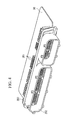
- FIG. 8 is a sectional view showing one example of a conventional holding member.
- a holding member 105 is a planar member that is formed by stamping out a metal sheet.
- the holding member 105 has such a shape that a pressed-in convex part 154 and a hooking part 153 are provided on both outsides of fixing leg part 152 extending in a fork shape from a head part 151.
- the hooking parts 153 penetrate the through hole 103 in the electric circuit board 101, and are caught by the electric circuit board 101.
- the connector 102 is held by the holding member 105 so as to avoid falling off the electric circuit board 101.
- the fixing leg part 152 is elastically deformed in the W direction, whereby the hooking parts 153 pass through the through hole 103 in the electric circuit board 101.
- the elastic deformation is small because the holding member 105 has a planar shape and the fixing leg part 152 is elastically deformed in a plane. Therefore, the through hole 103 in the electric circuit board 101 must be formed with high accuracy.
- the inner face of the through hole 103 in the electric circuit board 101 is usually copper-plated.
- the copper-plating is easily damaged by the contact of the edges of the fixing leg part 152 with the inner face of the through hole 103.
- the holding member is usually soldered to the electric circuit board by the solder flow process.
- the fixing of the holding member by soldering is required to be firm enough to prevent an excessive force from being applied to the terminal of the connector.
- This holding member has a configuration including a plate-shaped base part to be fixed to the electronic component, a pair of plate-shaped first leg parts facing to each other, which extend in almost the same direction from the base part, and are fitted in the through hole while interfering with the inner face of the through hole, and a plate-shaped second leg part which extends to between the paired first leg parts in the same direction as that of the first leg parts from the base part, and the edge faces of which face to the first leg parts.
- the paired first leg parts to be fitted in the through hole face to each other, when being fitted in the through hole, the first leg parts are elastically deformed in the thickness direction, not in the width direction. Therefore, the diameter of the through hole with accuracy lower than before can be accommodated, so that the productivity is improved. Also, on the inner face of the through hole, a copper-plating layer is usually formed. In the holding member of this invention, since the paired first leg parts come into surface contact with the inner face of the through hole so as to be displaced in the diameter direction of the through hole, the damage to the through hole can be reduced.
- the present invention has been accomplished in view of the above-described technical problems, and accordingly an object thereof is to provide a holding member the leg parts of which can be fitted in a through hole without damaging the inner face of the through hole while securing a high resistance force against a pulling-out force, and further which enables that the mounting of an electronic component to an electric circuit board after soldering is performed firmly. Another object of the present invention is to provide an electronic component provided with such the holding member.
- the present invention provides a holding member that is fitted in a through hole formed in an electric circuit board to hold an electronic component on the electric circuit board, the holding member including: a plate-shaped base part fixed to the electronic component; a pair of plate-shaped first leg parts that extend in almost the same direction from the base plate, and are fitted in the through hole while interfering with the inner face of the through hole; and a second leg part that is provided between the paired first leg parts and extends in the same direction as that of the first leg parts from the base part, wherein each of the first leg parts comprises a protruding part, which protrudes to the side opposite to the second leg part, in the tip portion of the first leg part; and each of the first leg parts comprises a groove or a penetrating slit in a middle portion between the side close to the second leg part and the side opposite to the second leg part.
- the first leg part has a rigidity decreased by the groove or the penetrating slit formed in the first leg part. Therefore, the first leg part is elastically deformed easily, when the first leg part is fitted in the through hole while interfering with the inner face of the through hole. Thus, strong interference with the inner face of the through hole can be restrained.
- solder can be sucked up through the groove or the penetrating slit.
- the above-described groove or penetrating slit has only to be formed in at least a part of the portion ranging from the side on which the first leg part comes close to the base part to a tip end portion in which the protruding part is formed. It is especially preferable that the groove or the penetrating slit be formed continuously in the portion ranging from the side on which the first leg part comes close to the base part to the tip end portion in which the protruding part is formed.
- the upper end portion of the groove or the penetrating slit is preferably located in the vicinity of the surface on the side where the electronic component is mounted to the electric circuit board, while the first leg part is fitted in the through hole,.
- Each of the paired first leg parts is preferably arranged at such a position that a gap, into which molten solder flows on account of the capillary action, is provided between the first leg part and the edge face of the second leg part. This ensures that molten solder is sucked up and soldering can be performed reliably.
- the present invention provides an electronic component held to an electric circuit board provided with a through hole, the electronic component including a holding member that has leg parts inserted into the through hole to hold the electronic component on the electric circuit board, the holding member including: a plate-shaped base part fixed to the electronic component; a pair of plate-shaped first leg parts that extend in almost the same direction from the base plate, and are fitted in the through hole while interfering with the inner face of the through hole; and a second leg part that is provided between the paired first leg parts and extends in the same direction as that of the first leg parts from the base part.
- Each of the first leg part comprises a protruding part, which protrudes to the side opposite to the second leg part, in the tip portion of the first leg part; and each of the first leg part comprises a groove or a penetrating slit in a middle portion between the side close to the second leg part and the side opposite to the second leg part.
- the first leg part since the first leg part has a rigidity decreased by the groove or the penetrating slit formed in the first leg part, when the first leg part is fitted in the through hole while interfering with the inner face of the through hole, the first leg part is elastically deformed easily. Therefore, strong interference with the inner face of the through hole can be restrained. Thereby, the leg parts of the holding member can be fitted in the through hole without damaging the inner face of the through hole. As a result, the protrusion dimension of the protruding part can be increased, so that a high resistance force is secured against a pulling-out force, and thereby the mounting of an electronic component to an electric circuit board after soldering can be performed firmly.
- solder can be sucked up through the groove or the penetrating slit, in this respect as well, the mounting of an electronic component to an electric circuit board after soldering can be performed firmly.
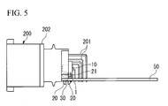
- a holding member 1 is fitted in a through hole 51 (refer to FIG. 2 ) formed in an electric circuit board 50 to hold a connector (electronic component) 200 on the electric circuit board 50.
- the holding member 1 is formed by stamping, pressing, and bending a brass sheet. Also, the holding member 1 is subjected to tin plating treatment so that the surface thereof is wetted by molten solder.
- the holding member 1 includes a base part 10, a pair of first leg parts 20, and a second leg part 30 provided between these paired first leg parts 20.
- the direction in which the two first leg parts 20 and the second leg part 30 are arranged is called the "width direction”.
- the base part 10 which has a rectangular shape, is pressed in a groove provided on the side surface of an insulating housing of the connector 200. At a side edge 11 of the base part 10, concave parts 12 are provided. Also, the base part 10 comprises a rib 13 for enhancing the bending strength, the rib 13 being formed by pressing.
- the paired plate-shaped first leg parts 20 are formed so as to extend in almost the same direction from one side of the base part 10. Also, the plate-shaped second leg part 30 extends in the direction identical to the extending direction of the first leg parts 20.
- the paired first leg parts 20 are fitted in the through hole 51 formed in the electric circuit board 50 while interfering with the through hole 51.
- Each of the paired first leg parts 20 is formed by bending an elongate sheet extending from an end portion of the base part 10.
- Each of the paired first leg parts 20 includes a deflection deformed part 21 extending from the base part 10, and a fitted-in part 22 extending continuously from the deflection deformed part 21.
- the deflection deformed part 21 includes a first parallel part 21b, a folded-back part 21c, and a second parallel part 21d.
- the first parallel part 21b extends to the side opposite to the second leg part 30 from a base part 21a bent through approximate 90 degrees from the base part 10 so as to be substantially parallel to a mounting surface 50a.
- the first parallel part 21b is substantially perpendicular to the base part 10 and substantially parallel to the mounting surface 50a.
- the folded-back part 21c is folded back substantially into a U shape from the first parallel part 21b.
- the second parallel part 21d extends from the folded-back part 21c to the second leg part 30 side and is substantially perpendicular to the base part 10 and substantially parallel to the mounting surface 50a.
- the band-shaped deflection deformed part 21 is formed so as to orthogonally intersect the base part 10, so that when the fitted-in part 22 of the first leg part 20 is displaced to the direction such as to be brought close to and away from the second leg part 30, the deflection deformed part 21 is elastically deformed easily in the thickness direction.
- the fitted-in part 22 is a part that is fitted in the through hole 51.
- the fitted-in part 22 is bent through approximate 90 degrees from the second parallel part 21d, and is formed so as to be parallel to the base part 10 and extend almost perpendicularly to the mounting surface 50a.
- a protruding part 26 protruding to the side opposite to the second leg part 30 is formed.
- the fitted-in part 22 has a tapered shape such that the width thereof increases gradually from a tip end 22a toward the protruding part 26.
- the protruding part 26 penetrates the through hole 51 and engages with the opposite surface of the electric circuit board 50.
- the fitted-in part 22 and the protruding part 26 comprises a slit (penetrating slit) 27 penetrating in the plate thickness direction.
- a slit penetrating slit
- the configuration is made such that the fitted-in part 22 and the protruding part 26 are formed by a beam-like member 28 having a substantially fixed width that extends along the outline thereof.
- the first leg part 20 is a spring supported by the base part 10, and the whole thereof is turned with the base part 10 being the center, and the tip end portion of the fitted-in part 22 is elastically displaced in the width direction. Further, in the first leg part 20, by the slit 27, an outside beam part 28a located on the outside in the width direction (on the side opposite to the second leg part 30) and an inside beam part 28b located on the inside in the width direction (on the second leg part 30 side) can be elastically deformed respectively.
- the second leg part 30 extends to between the paired first leg parts 20 in the same direction as that of the first leg part 20 from the base part 10. More specifically, the second leg part 30 includes a connecting part 31 that is bent through approximate 90 degrees from the base part 10 and extends, and a fitted-in part 32 that is bent through approximate 90 degrees from the connecting part 31 and extends continuously with the connecting part 31.
- the fitted-in part 32 is inserted into the through hole 51 in the electric circuit board 50. Since the second leg part 30 is arranged between the paired first leg parts 20, even when being inserted into the through hole 51 in the electric circuit board 50 together with the paired first leg parts 20, the second leg part 30 does not interfere directly with the inner face of the through hole 51.
- a gap between an edge face 33 of the second leg part 30 and the first leg part 20 has such a width that molten solder flows therein on account of the capillary action. More specifically, the average width can be made, for example, about 0.4 mm.
- the electric circuit board 50 in which the above-described holding member 1 is fitted comprises the through hole 51.
- a copper-plating layer 52 is formed on the inner face of the through hole 51 and on the electric circuit board 50 in the vicinity of the through hole 51.
- the thickness of the electric circuit board 50 is preferably not smaller than 1.2 mm and not larger than 1.6 mm.
- the holding member 1 is pushed into the arrow-marked direction from the mounting surface 50a side of the electric circuit board 50, whereby the holding member 1 is inserted into the through hole 51. Specifically, the paired first leg parts 20 and the second leg part 30 are inserted into the through hole 51.
- the two first leg parts 20 are elastically deformed to the side of the second leg part 30 on the inside in the width direction, and resultantly the protruding parts 26 protruding to opposite sides are displaced to the inside in the width direction and pass through the through hole 51.
- the first leg parts 20 having been elastically deformed to the inside in the width direction return to the outside in the width direction.
- the protruding parts 26 engage with a soldering surface 50b of the electric circuit board 50. Resultantly, even if the electric circuit board 50 is turned over before soldering, the holding member 1 holds the connector 200 so that the connector 200 does not fall under its own weight. Viewing from the connector 200 side, the connector 200 holds the electric circuit board 50.
- the slit 27 be formed so that an upper end portion 27a thereof is located in the vicinity of the mounting surface 50a of the electric circuit board 50, further preferably, at a position projecting upward from the mounting surface 50a.
- the holding member 1 When the holding member 1 is fitted in the through hole 51 as described above, since the first leg parts 20 have a rigidity decreased by the slit 27, when passing through the through hole 51, the protruding parts 26 are elastically deformed easily. Therefore, even if the protrusion dimensions of the protruding parts 26 are increased to make the holding member 1 less liable to be removed, the interference of the first leg part 20 with the copper-plating layer 52 of the through hole 51 can be weakened. Thereby, the damage to the copper-plating layer 52 of the through hole 51 can be reduced. In order to make the holding member 1 less liable to be removed, it is necessary to increase the dimensions projecting to opposite sides in the width direction of the protruding parts 26.
- the connector 200 held to the electric circuit board 50 by the holding member 1 is mounted to the electric circuit board 50 incorporated in an electronic equipment.
- the connector 200 electrically connects the circuit on the electric circuit board 50 to a circuit other than the circuit on the electric circuit board 50.
- the connector 200 includes contacts 201 connected to the circuit on the electric circuit board 50, and a housing 202 for fixing the holding member 1 and the contacts 201. By pressing the base part 10 of the holding member 1 in a groove (not shown) provided in the connector 200, the holding member 1 is attached to the connector 200.
- the connector 200 is held to the electric circuit board 50.
- the holding member 1 is soldered to the electric circuit board 50 together with the terminal of the connector 200. Thereby, the connector 200 is held to the electric circuit board 50.
- the soldering surface 50b of the electric circuit board 50 is immersed in molten solder while the holding member 1 is fitted in the through hole 51. Then, the copper-plating layer 52 of the through hole 51 and the holding member 1 are wetted by molten solder. The molten solder spreads on the surfaces of the first leg parts 20 and on the copper-plating layer 52 of the through hole 51 and is sucked up into the through hole 51. Since the second leg part 30 is arranged between the first leg parts 20, the molten solder also spreads on the surface of the second leg part 30 and is sucked up.
- the gap between the edge face 33 of the second leg part 30 and the first leg part 20 has a width such that molten solder flows therein on account of the capillary action. Therefore, the molten solder spreads in the gaps between the edge faces 33 of the second leg part 30 and the first leg parts 20 and is sucked up on account of the capillary action. Further, the molten solder is also sucked up by the capillary action through the slits 27 formed in the first leg parts 20.
- the molten solder sucked up into the through hole 51 spreads on the surfaces of the second parallel parts 21d of the first leg parts 20 and rises up to the mounting surface 50a.
- solder fillet 70 that covers the second parallel part 21d of the first leg part 20 and the mounting surface 50a of the electric circuit board 50 is formed on the mounting surface 50a of the electric circuit board 50.
- the molten solder is also sucked up by the capillary action through the slits 27 formed in the first leg parts 20.
- the upper end portion 27a of the slit 27 is located in the vicinity of the mounting surface 50a of the electric circuit board 50 while the holding member 1 is fitted in the through hole 51 and the protruding parts 26 engage with the soldering surface 50b of the electric circuit board 50. Thereby, the fillet 70 can be formed more satisfactorily.
- the connector 200 is fixed to the electric circuit board 50.
- the configuration is made such that the slit 27 is formed in the first leg part 20.
- a slit (penetrating slit) 27' may be formed in only the region of the first leg part 20 that is close to the base part 10 without forming a slit 27' in the protruding part 26.
- a slit (penetrating slit) 27" may be formed in only the portion of the protruding part 26.
- the slit 27 may be formed so that the depth thereof is different depending on the place.
- the configuration can be made such that the slit 27 is penetrated in the portion of the protruding part 26, and is not penetrated in the region of the first leg part 20 that is close to the base part 10 side beyond the protruding part 26.
- the first leg part 20 described above may comprise a groove in place of the slit 27, and the cross-sectional shape of the groove can be made a U-like shape, an H shape, and the like. Needless to say, the cross-sectional shape of the groove may be a shape other than the above-described shapes.
- the connector 200 has been explained as one example of the electronic component in accordance with the present invention.
- the present invention is not limited to the connector, and can be applied to any other electronic component held to the electric circuit board 50 by the holding member.
- soldering is performed by the solder flow process.
- the present invention is not limited to the solder flow process.
- the soldering can be performed by the solder reflow process by filling the through hole 51 beforehand with solder paste.
- the present invention is not limited to this configuration.
- the second leg part 30 that does not interfere with the copper-plating layer 52 of the through hole 51 is configured so that the edge faces 33 thereof face to the first leg parts 20, the second leg part 30 may be arranged without being restricted by the shape of the through hole 51 and the shape of the first leg part 20.
- the second leg part 30 by arranging the second leg part 30 with the gap into which molten solder flows on account of the capillary action being provided, molten solder can be made further liable to be sucked up into the through hole 51.
- the holding member 1 that is made of brass and tin-plated has been explained.
- the present invention is not limited to this holding member 1.
- the holding member has only to be made of a metal the surface of which is wetted by molten solder. For example, if being made of a copper alloy, the holding member need not be subjected to tin plating treatment.
Landscapes
- Coupling Device And Connection With Printed Circuit (AREA)
Applications Claiming Priority (1)
| Application Number | Priority Date | Filing Date | Title |
|---|---|---|---|
| JP2010248538A JP2012099440A (ja) | 2010-11-05 | 2010-11-05 | 保持部材、電子部品 |
Publications (1)
| Publication Number | Publication Date |
|---|---|
| EP2451015A1 true EP2451015A1 (de) | 2012-05-09 |
Family
ID=45047594
Family Applications (1)
| Application Number | Title | Priority Date | Filing Date |
|---|---|---|---|
| EP11187905A Withdrawn EP2451015A1 (de) | 2010-11-05 | 2011-11-04 | Halteelement und elektronische Komponente |
Country Status (3)
| Country | Link |
|---|---|
| EP (1) | EP2451015A1 (de) |
| JP (1) | JP2012099440A (de) |
| CN (1) | CN102544941A (de) |
Cited By (1)
| Publication number | Priority date | Publication date | Assignee | Title |
|---|---|---|---|---|
| DE102013222919B4 (de) | 2012-12-04 | 2022-03-24 | Denso Corporation | Verbinder |
Families Citing this family (3)
| Publication number | Priority date | Publication date | Assignee | Title |
|---|---|---|---|---|
| JP2017022043A (ja) * | 2015-07-14 | 2017-01-26 | 住友電装株式会社 | コネクタ実装基板 |
| CN109346888B (zh) * | 2018-11-26 | 2023-11-28 | 大连派欧机电设备有限公司 | 一种多媒体接口固定机构及连接方法 |
| JP7482021B2 (ja) | 2020-12-25 | 2024-05-13 | 日本航空電子工業株式会社 | 電気部品 |
Citations (7)
| Publication number | Priority date | Publication date | Assignee | Title |
|---|---|---|---|---|
| JPH0662486U (ja) | 1993-02-09 | 1994-09-02 | 第一電子工業株式会社 | コネクタの固定金具 |
| JPH09274975A (ja) | 1996-04-04 | 1997-10-21 | Fujitsu Takamizawa Component Kk | 基板実装型コネクタ |
| JPH1040979A (ja) | 1996-03-29 | 1998-02-13 | Berg Technol Inc | 電気コネクタをプリント基板に固定するための装置 |
| JPH10162886A (ja) | 1996-06-26 | 1998-06-19 | Whitaker Corp:The | 電気コネクタ |
| US5904581A (en) * | 1996-07-17 | 1999-05-18 | Minnesota Mining And Manufacturing Company | Electrical interconnection system and device |
| JP2007128772A (ja) | 2005-11-04 | 2007-05-24 | Tyco Electronics Amp Kk | 保持部材、実装構造、および電子部品 |
| JP2009170310A (ja) | 2008-01-17 | 2009-07-30 | Denso Corp | 保持部材、電子部品、及び電子装置 |
-
2010
- 2010-11-05 JP JP2010248538A patent/JP2012099440A/ja active Pending
-
2011
- 2011-11-02 CN CN2011103661750A patent/CN102544941A/zh active Pending
- 2011-11-04 EP EP11187905A patent/EP2451015A1/de not_active Withdrawn
Patent Citations (7)
| Publication number | Priority date | Publication date | Assignee | Title |
|---|---|---|---|---|
| JPH0662486U (ja) | 1993-02-09 | 1994-09-02 | 第一電子工業株式会社 | コネクタの固定金具 |
| JPH1040979A (ja) | 1996-03-29 | 1998-02-13 | Berg Technol Inc | 電気コネクタをプリント基板に固定するための装置 |
| JPH09274975A (ja) | 1996-04-04 | 1997-10-21 | Fujitsu Takamizawa Component Kk | 基板実装型コネクタ |
| JPH10162886A (ja) | 1996-06-26 | 1998-06-19 | Whitaker Corp:The | 電気コネクタ |
| US5904581A (en) * | 1996-07-17 | 1999-05-18 | Minnesota Mining And Manufacturing Company | Electrical interconnection system and device |
| JP2007128772A (ja) | 2005-11-04 | 2007-05-24 | Tyco Electronics Amp Kk | 保持部材、実装構造、および電子部品 |
| JP2009170310A (ja) | 2008-01-17 | 2009-07-30 | Denso Corp | 保持部材、電子部品、及び電子装置 |
Cited By (1)
| Publication number | Priority date | Publication date | Assignee | Title |
|---|---|---|---|---|
| DE102013222919B4 (de) | 2012-12-04 | 2022-03-24 | Denso Corporation | Verbinder |
Also Published As
| Publication number | Publication date |
|---|---|
| CN102544941A (zh) | 2012-07-04 |
| JP2012099440A (ja) | 2012-05-24 |
Similar Documents
| Publication | Publication Date | Title |
|---|---|---|
| US7744408B2 (en) | Holding member, mounting structure in which holding member is mounted on electronic circuit board, and electronic component including holding member | |
| EP1947739A1 (de) | Halteelement, verpackungsstruktur und elektronische komponente | |
| EP2259381B1 (de) | Halteglied, anbringstruktur, die das halteglied in einer elektrischen leiterplatte angebracht aufweist, und elektronisches teil mit dem halteglied | |
| US7621784B2 (en) | Socket contact | |
| US9668347B2 (en) | Electric part soldered onto printed circuit board | |
| EP0532974B1 (de) | Elektrische Teile für Oberflächenmontage | |
| EP2451015A1 (de) | Halteelement und elektronische Komponente | |
| CN108390173B (zh) | 基板用连接器 | |
| US5823801A (en) | Electrical connector having thin contacts with surface mount edges | |
| US20150180149A1 (en) | Electrical connector | |
| KR20160029117A (ko) | 측면 엑세스 종결 패드를 갖는 인쇄 회로 기판 | |
| JP6024428B2 (ja) | 保持部材及びコネクタ | |
| EP2239818A1 (de) | Halteelement, in eine elektrische leiterplatte integrierte montagestruktur mit dem halteelement und elektronikteil mit dem halteelement | |
| US11394143B2 (en) | Connector | |
| KR101625691B1 (ko) | 회로 기판용 전기 커넥터 | |
| JP3130784B2 (ja) | 電子部品の端子構造 | |
| US20200021047A1 (en) | Press-fit terminal and substrate assembly | |
| JP6053146B2 (ja) | コネクタ | |
| JP2001052788A (ja) | Fpcとプリント基板間の電気コネクタ装置 | |
| US20050277332A1 (en) | Surface mountable electrical connector | |
| JP6440345B2 (ja) | コネクタ | |
| JP6095412B2 (ja) | コネクタ | |
| JP6864887B2 (ja) | 取付具 | |
| JP4823942B2 (ja) | チップ形電子部品 | |
| JP3919520B2 (ja) | 電子回路装置 |
Legal Events
| Date | Code | Title | Description |
|---|---|---|---|
| PUAI | Public reference made under article 153(3) epc to a published international application that has entered the european phase |
Free format text: ORIGINAL CODE: 0009012 |
|
| AK | Designated contracting states |
Kind code of ref document: A1 Designated state(s): AL AT BE BG CH CY CZ DE DK EE ES FI FR GB GR HR HU IE IS IT LI LT LU LV MC MK MT NL NO PL PT RO RS SE SI SK SM TR |
|
| AX | Request for extension of the european patent |
Extension state: BA ME |
|
| 17P | Request for examination filed |
Effective date: 20121107 |
|
| STAA | Information on the status of an ep patent application or granted ep patent |
Free format text: STATUS: THE APPLICATION HAS BEEN WITHDRAWN |
|
| 18W | Application withdrawn |
Effective date: 20130709 |