EP1883153A2 - Umrichter - Google Patents
Umrichter Download PDFInfo
- Publication number
- EP1883153A2 EP1883153A2 EP07014788A EP07014788A EP1883153A2 EP 1883153 A2 EP1883153 A2 EP 1883153A2 EP 07014788 A EP07014788 A EP 07014788A EP 07014788 A EP07014788 A EP 07014788A EP 1883153 A2 EP1883153 A2 EP 1883153A2
- Authority
- EP
- European Patent Office
- Prior art keywords
- inverter
- output voltage
- circuit
- output
- switching elements
- Prior art date
- Legal status (The legal status is an assumption and is not a legal conclusion. Google has not performed a legal analysis and makes no representation as to the accuracy of the status listed.)
- Withdrawn
Links
- 238000001514 detection method Methods 0.000 abstract description 13
- 239000003990 capacitor Substances 0.000 description 14
- 238000010586 diagram Methods 0.000 description 4
- ATJFFYVFTNAWJD-UHFFFAOYSA-N Tin Chemical group [Sn] ATJFFYVFTNAWJD-UHFFFAOYSA-N 0.000 description 3
- 230000006378 damage Effects 0.000 description 3
- 230000007423 decrease Effects 0.000 description 3
- 230000004048 modification Effects 0.000 description 3
- 238000012986 modification Methods 0.000 description 3
- 238000007796 conventional method Methods 0.000 description 1
- 230000000694 effects Effects 0.000 description 1
- 230000005669 field effect Effects 0.000 description 1
- 230000001788 irregular Effects 0.000 description 1
- 229910044991 metal oxide Inorganic materials 0.000 description 1
- 150000004706 metal oxides Chemical class 0.000 description 1
- 238000000034 method Methods 0.000 description 1
- 239000004065 semiconductor Substances 0.000 description 1
- 230000007704 transition Effects 0.000 description 1
Images




Classifications
-
- H—ELECTRICITY
- H02—GENERATION; CONVERSION OR DISTRIBUTION OF ELECTRIC POWER
- H02M—APPARATUS FOR CONVERSION BETWEEN AC AND AC, BETWEEN AC AND DC, OR BETWEEN DC AND DC, AND FOR USE WITH MAINS OR SIMILAR POWER SUPPLY SYSTEMS; CONVERSION OF DC OR AC INPUT POWER INTO SURGE OUTPUT POWER; CONTROL OR REGULATION THEREOF
- H02M1/00—Details of apparatus for conversion
- H02M1/32—Means for protecting converters other than automatic disconnection
-
- H—ELECTRICITY
- H02—GENERATION; CONVERSION OR DISTRIBUTION OF ELECTRIC POWER
- H02M—APPARATUS FOR CONVERSION BETWEEN AC AND AC, BETWEEN AC AND DC, OR BETWEEN DC AND DC, AND FOR USE WITH MAINS OR SIMILAR POWER SUPPLY SYSTEMS; CONVERSION OF DC OR AC INPUT POWER INTO SURGE OUTPUT POWER; CONTROL OR REGULATION THEREOF
- H02M1/00—Details of apparatus for conversion
- H02M1/36—Means for starting or stopping converters
-
- H—ELECTRICITY
- H02—GENERATION; CONVERSION OR DISTRIBUTION OF ELECTRIC POWER
- H02M—APPARATUS FOR CONVERSION BETWEEN AC AND AC, BETWEEN AC AND DC, OR BETWEEN DC AND DC, AND FOR USE WITH MAINS OR SIMILAR POWER SUPPLY SYSTEMS; CONVERSION OF DC OR AC INPUT POWER INTO SURGE OUTPUT POWER; CONTROL OR REGULATION THEREOF
- H02M7/00—Conversion of AC power input into DC power output; Conversion of DC power input into AC power output
- H02M7/42—Conversion of DC power input into AC power output without possibility of reversal
- H02M7/44—Conversion of DC power input into AC power output without possibility of reversal by static converters
- H02M7/48—Conversion of DC power input into AC power output without possibility of reversal by static converters using discharge tubes with control electrode or semiconductor devices with control electrode
- H02M7/53—Conversion of DC power input into AC power output without possibility of reversal by static converters using discharge tubes with control electrode or semiconductor devices with control electrode using devices of a triode or transistor type requiring continuous application of a control signal
- H02M7/537—Conversion of DC power input into AC power output without possibility of reversal by static converters using discharge tubes with control electrode or semiconductor devices with control electrode using devices of a triode or transistor type requiring continuous application of a control signal using semiconductor devices only, e.g. single switched pulse inverters
- H02M7/5387—Conversion of DC power input into AC power output without possibility of reversal by static converters using discharge tubes with control electrode or semiconductor devices with control electrode using devices of a triode or transistor type requiring continuous application of a control signal using semiconductor devices only, e.g. single switched pulse inverters in a bridge configuration
-
- H—ELECTRICITY
- H02—GENERATION; CONVERSION OR DISTRIBUTION OF ELECTRIC POWER
- H02M—APPARATUS FOR CONVERSION BETWEEN AC AND AC, BETWEEN AC AND DC, OR BETWEEN DC AND DC, AND FOR USE WITH MAINS OR SIMILAR POWER SUPPLY SYSTEMS; CONVERSION OF DC OR AC INPUT POWER INTO SURGE OUTPUT POWER; CONTROL OR REGULATION THEREOF
- H02M1/00—Details of apparatus for conversion
- H02M1/0067—Converter structures employing plural converter units, other than for parallel operation of the units on a single load
- H02M1/007—Plural converter units in cascade
Definitions
- the present invention contains subject matter related to Japanese Patent Application JP 2006-206660 filed in the Japanese Patent Office on July 28, 2006, the entire contents of which being incorporated herein by reference.
- the present invention relates to an inverter for converting DC voltage to AC voltage and outputting the AC voltage.
- Japanese Unexamined Patent Application Publication No. 2002-335678 discloses an inverter in which generation of excessive rush current upon start of an inverter is prevented by making output AC voltage having a sine wave always start from 0V at the time of starting the inverter as shown in Fig. 8.
- Japanese Patent No. 3,362,666 also discloses an inverter. AC output current from the inverter is detected at any time. In the case where the AC output current becomes larger than a predetermined first threshold, before the AC output current reaches a second threshold larger than the first threshold, flow of excessive current is allowed for a while.
- An inverter of an embodiment of the present invention is provided to drive a load including a capacitive element in an input stage and includes: an inverter circuit converting a DC input voltage to an AC output voltage; current detecting means for detecting AC output current flowing out from the inverter circuit; and control means, in the case where detected AC output current comes to have a predetermined value or larger, for controlling the inverter circuit so as to reset the AC output voltage to 0V and then re-start its operation.
- a DC input voltage is converted to an AC output voltage by the inverter circuit, and AC output current flowing out from the inverter circuit is detected by the current detecting means.
- the inverter circuit is controlled so as to reset the AC output voltage to 0V and then re-start its operation.
- the inverter of the embodiment of the invention may include a full-bridge-type switching circuit having four switching elements, and a pair of charge pump circuits each connected to each of a pair of high-side switching elements of the four switching elements.
- the control means controls the inverter circuit so that the AC output voltage immediately after re-start has a polarity opposite to that of output voltage immediately before reset.
- it is unnecessary to invert the polarity of voltage supplied from the charge pump circuit to the pair of switching elements on the high voltage side. Consequently, the operation can be re-started quicker as compared with the case of re-starting operation with the polarity opposite to that of the output voltage immediately before reset.
- a pair of independent power supply circuits each may be connected to each of the pair of high-side switching elements.
- the control means may control so that the AC output voltage immediately after re-start comes to have a polarity opposite to that of the voltage immediately before reset.
- An "independent power supply circuit” is different from, for example, a power supply circuit of the charge pump circuit or the like and does not generate a voltage based on another power supply voltage, but denotes a power supply circuit generating a voltage independently of other power supply voltages.
- the inverter circuit includes a full-bridge-type switching circuit having a pair of first switching elements for switching polarity of the AC output voltage and a pair of second switching elements for generating pulse voltage on the basis of the DC input voltage, and the first switching element is constructed by a bipolar transistor, it is preferable to control so that AC output voltage immediately after re-start has a polarity opposite to that of output voltage immediately before reset.
- the pair of first switching elements is turned off and the other one is turned on.
- the control means may stop the operation of the circuit.
- the control means may stop the operation of the circuit.
- the control means may stop the operation when the number of re-start times of operation reaches the predetermined number of times within the predetermined time.
- erroneous stop in the case such that the number of re-start times reaches the predetermined number of times after lapse of long time can be avoided.
- AC output current flowing out from the inverter circuit can be detected by the current detecting means.
- the inverter circuit is controlled so as to reset the AC output voltage to 0V and then re-start its operation. Therefore, for example, in the case of connecting a load including a capacitive element in an input stage during operation of the inverter or in the case where the load includes a standby circuit, generation of rush current can be prevented. Since generation of rush current can be prevented, a device having a margin of electric property smaller than that of a conventional device can be applied as a device in the inverter. Thus, generation of excessive rush current can be prevented with a simple configuration.
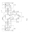
- Fig. 1 shows the configuration of a power supply system including an inverter according to an embodiment of the present invention.
- the power supply system generates an AC output voltage Vacout on the basis of a DC input voltage Vdcin input from an input terminal Tin, outputs the AC output voltage Vacout from an output terminal Tout, and drives a load 3 of a capacitor-input-type rectifier constructed by, for example, a PC, a TV apparatus, and the like, and is applied to, for example, a vehicle or the like.
- the power supply system has an input filter circuit 11, a DC/DC converter 12, a voltage control circuit 13, and an inverter 2.
- the input filter circuit 11 is a circuit eliminating noise of the DC input voltage Vdcin input from the input terminal Tin and is constructed by, for example, a choke coil, a capacitor, and the like.
- the DC/DC converter 12 converts the DC input voltage Vdcin passed through the input filter circuit 11 to a DC output voltage Vdcout.
- the DC/DC converter 12 includes, for example, a switching element, a transformer, and the like.
- the voltage control circuit 13 detects, at ay time, the DC output voltage Vdcout output from the DC/DC converter 12 and controls the DC/DC converter 12 so that the DC output voltage Vdcout maintains a predetermined value.
- the on duty ratio of the switching element is controlled in accordance with the magnitude of the DC output voltage Vdcout.
- the inverter 2 generates the AC output voltage Vacout o the basis of the DC output voltage Vdcout output from the DC/DC converter 12 and outputs the AC output voltage Vacout from the output terminal Tout.
- the inverter 2 has a DC/AC inverter 21, an output filter circuit 22, a current detection circuit 23, a reset control unit 24, a counter 25, a shutdown control unit 26, a timer circuit 27, and a drive pulse generation circuit 28.
- the DC/AC inverter 21 generates a pulse output voltage Vpout having a pulse-shaped voltage waveform on the basis of the DC output voltage Vdcout.
- the DC/AC inverter 21 will be described in detail later.
- the output filter circuit 22 generates the AC output voltage Vacout having a sine wave on the basis of the pulse output voltage Vpout output from the DC/AC inverter 21 and is constructed by, for example, a choke coil, a capacitor, and the like.
- the current detection circuit 23 detects, at any time, an AC output current Iacout flowed from the output filter circuit 22 and, in the case where the absolute value of the AC output current Iacout becomes excessive and equal to or larger than a predetermined threshold Ith which will be described later, outputs an excessive current detection signal indicative of the fact to the reset control unit 24.
- the reset control unit 24 controls the drive pulse generation circuit 28 to be described later to once drop an output voltage (pulse output voltage Vpout) from the DC/AC inverter 21 to 0V (reset the operation of the DC/AC inverter 21) and, after that, re-start the operation.
- the reset control unit 24 outputs a reset signal indicative of the re-start to the counter 25.
- the counter 25 counts the number of generation times of the reset signal output from the reset control unit 24 (the number of re-starting times of operation of the DC/AC inverter 21), and outputs the count value to the shutdown control unit 26.
- the shutdown control unit 26 controls the operation of the DC/DC converter 12 and the drive pulse generation circuit 28 so that the operation of the DC/DC converter 12 and the drive pulse generation circuit 28 stops.
- the timer circuit 27 measures predetermined time lapsed since a first reset signal as a trigger output from the counter 25 is generated.
- the shutdown control unit 26 stops the operation of the DC/DC converter 12 and the DC/AC inverter 21.
- the drive pulse generation circuit 28 generates a drive pulse for performing PWM (Pulse Width Modulation) on the switching element (which will be described later) in the DC/AC inverter 21, thereby controlling the magnitude and cycle of the pulse output voltage Vpout from the DC/AC inverter 21 and the AC output voltage Vacout from the output filter circuit 22.
- PWM Pulse Width Modulation
- the DC/AC inverter 21 has a full-bridge-type switching circuit 210 including four switching elements SW1 to SW4, two charge pump circuits 211 and 213, and two drivers 212 and 214.
- the switching elements SW1 and SW3 are constructed by N-channel-type MOS-FETs (Metal Oxide Semiconductor-Field Effect Transistors).
- the gate of the switching element SW1 is connected to the output terminal of the driver 212, the source is connected to connection points P5 and P3, and the drain is connected to a power supply line of the DC output voltage Vdcout via a connection point P1.
- the gate of the switching element SW3 is connected to the output terminal of the driver 214, the source is connected to connection points P6 and P4, and the drain is connected to the power supply line of the DC output voltage Vdcout via the connection point P1.
- Each of the switching elements SW1 and SW3 plays the role of, as will be specifically described later, generating the pulse output voltage Vpout from the DC output voltage Vdcout by its on/off operation.
- the switching elements SW2 and SW4 are constructed by NPN-type IBGTs.
- a drive pulse signal SP2 from the drive pulse generation circuit 28 which will be described later is input.
- the emitter of the switching element SW2 is grounded via a connection point P2, and the collector is connected to the connection points P3 and P5.
- a drive pulse signal SP4 from the drive pulse generation circuit 28 which will be described later is input.
- the emitter of the switching element SW4 is grounded via the connection point P2, and the collector is connected to the connection points P4 and P5.
- the charge pump circuit 211 has a diode D1 and a capacitor C1.
- the anode of the diode D1 is connected to a power supply Vcc for driving the gates of the switching elements SW2 and SW4, and the cathode is connected to one end of the capacitor C1 and a high-voltage-side input terminal of the driver 212, and the other end of the capacitor C1 is connected to a low-voltage-side input terminal of the driver 212 and the connection point P5.
- the charge pump circuit 213 similarly has a diode D3 and a capacitor C3.
- the anode of the diode d3 is connected to the power supply Vcc, the cathode is connected to one end of the capacitor C3 and a high-voltage-side input terminal of the driver 214, and the other end of the capacitor C3 is connected to a low-voltage-side input terminal of the driver 214 and the connection point P6.
- the charge pump circuits 211 and 213 function as a booster circuit generating a voltage that drives the drivers 212 and 214 and the gates of the switching elements SW1 and SW3 by accumulating charges in the capacitors C1 and C3 by current paths I1 and I3 shown in the diagram on the basis of the power supply Vcc.
- the drivers 212 and 214 drive the switching elements SW1 and SW3 on the basis of drive pulse signals SP1 and SP3 from the drive pulse generation circuit 28, respectively.
- the DC/AC inverter 21 and the output filter circuit 22 correspond to an example of "an inverter circuit” in the present invention
- the reset control unit 24, the counter 25, the shutdown control unit 26, the timer circuit 27, and the drive pulse generation circuit 28 correspond to an example of "control means” in the invention.
- the switching elements SW1 and SW3 correspond to an example of "a pair of switching elements on the high voltage side” and "a pair of second switching elements” in the invention.
- the switching elements SW2 and SW4 correspond to an example of "a pair of first switching elements" in the invention.
- Fig. 3 is a timing waveform chart showing an example of the basic operation of the inverter 2.
- A shows the DC output voltage Vdcout
- B shows the pulse output voltage Vpout
- C shows the AC output voltage Vacout.
- the switching elements SW1 to SW4 in the switching circuit 210 perform predetermined PWM operation by the drive pulses SP1 to SP4 output from the drive pulse generation circuit 28 and drive signals from the drivers 212 and 214 receiving power from the charge pump circuits 211 and 213, and the pulse output voltage Vpout is generated on the basis of the DC output voltage Vdcout supplied from the connection points P1 and P2 and is output from the connection points P3 and P4.
- the switching elements SW2 and SW3 are always in an off state and the switching element SW4 switching the polarity of the pulse output voltage Vpout (and the AC output voltage Vacout) is always in the on state.
- the switching element SW1 performs the PWM operation.
- the pulse output voltage Vpout as shown in FIG. 3 (B) is generated on the basis of the predetermined DC output voltage Vdcout (FIG. 3 (A)).
- the pulse output voltlage Vpout is controlled so that the pulse width gradually increases (so that the duty ratio increases) in the period of the timing t0 to timing t1.
- the AC output voltage Vacout output from the output filter circuit 22 has a sine wave which crosses a zero cross point Z1 of 0V at the timing t0 and monotonously increases as shown in Fig. 3 (C).
- the pulse output voltage Vpout is controlled so that the pulse width of the pulse output voltage Vpout gradually decreases (so that the duty ratio gradually decreases).
- the AC output voltage Vacout has a sine wave which monotonously decreases and crosses a zero cross point Z2 at the timing t2 as shown in Fig. 3 (C).
- a pulse output voltage Vpout having the negative polarity using the connection point P4 as a reference is output.
- the switching elements SW1 and SW4 are always in an off state and the switching element SW2 switching the polarity of the pulse output voltage Vpout (and the AC output voltage Vacout) is always in the on state.
- the switching element SW3 performs the PWM operation. Therefore, as shown in Figs. 3 (B) and (C), the pulse output voltage Vpout and the AC output voltage Vacout having the negative polarity are generated.
- the period of timing t0 to timing t4 corresponds to an operation cycle T of the pulse output voltage Vpout and the AC output voltage Vacout.
- timing t4 The operation after the timing t4 is similar to the above. That is, in the period of timing t4 to timing t5, the pulse output voltage Vpout and the AC output voltage Vacout having the positive polarity are generated. In the "T/2" cycle from the timing t5, the pulse output voltage Vpout and the AC output voltage Vacout having the negative polarity are generated.
- the load 3 is driven.
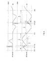
- FIG. 4 is a timing waveform chart showing an example of the reset control operation of the inverter 2.
- (A) shows the AC output current Iacout
- (B) shows the AC output voltage Vacout.
- the AC output current Iacout flowed from the output filter circuit 22 is detected by the current detection circuit 23 at any time as shown in Fig. 4 (A).
- the reset control unit 24 control the operation of the drive pulse generation circuit 28 so that the output voltage (pulse output voltage Vpout) of the DC/AC inverter 21 and the AC output voltage Vacout based on the pulse output voltage Vpout become 0V as shown by arrow G1 in Fig. 4 (B) (so that the operation of the DC/AC inverter 21 is reset).
- the switching elements SW1 and SW3 are turned off by the drive pulses SP1 to SP4 and the switching elements SW2 and SW4 are turned on.
- the reset control unit 24 controls the operation of the drive pulse generation circuit 28 with the drive pulses SP1 to SP4 so that the switching elements SW1 to SW4 re-start the normal operation and the DC/AC inverter 21 re-starts the normal operation. Therefore, as shown in Fig. 4 (B), after the timing t12, the AC output voltage Vacout having a sine wave like the original one is output, and the period of timing t12 to timing t13 is the half of the new operation cycle T. Each time the DC/AC inverter 21 re-starts the operation as described above (the operation is reset), a reset signal is output from the reset control unit 24 to the counter 25.
- the AC output voltage Vacout immediately after re-start of the operation has the same polarity as that of the voltage immediately before reset (the AC output voltage Vacout in the period of timing t10 to timing t11). Therefore, it is unnecessary for the charge pump circuits 211 and 213 to change the charging timing of the capacitors C1 and C3 and to invert the polarity of a signal supplied to the drivers 212 and 214. The operation is re-started quicker than that in the case of re-starting the operation with the polarity opposite to that of the voltage immediately before reset.
- the excessive current detection signal is output from the current detection circuit 23 to the reset control unit 24.
- the reset control unit 24 controls the operation of the drive pulse generation circuit 28 so that the AC output voltage Vacout becomes 0V as shown by arrow G2 in Fig. 4 (B).
- the DC/AC inverter 21 is controlled to re-start the normal operation at timing t15.
- the AC output voltage Vacout having a sine wave like the original one is output.
- the period of timing t15 to timing t16 is equal to the half of a new operation cycle T.
- the DC/AC inverter 21 is controlled by the reset control unit 24 and the drive pulse generation circuit 28 so as to re-start the operation after the AC output voltage Vacout becomes 0V.
- the counter 25 counts the number of generation times of the reset signal output from the reset control unit 24 (the number of re-starting times of the DC/AC inverter 21) at any time, and the count value is output to the shutdown control unit 26.
- the timer circuit 27 uses the first reset signal output from the counter 25 as a trigger and measures predetermined time since the signal is generated.
- the shutdown control unit 26 controls the operation of the DC/DC converter 12 and the drive pulse generation circuit 28. As a result, the operation of the DC/DC converter 12 and the DC/AC inverter 21 stops.
- the AC output current Iacout flowed from the output filter circuit 22 is detected by the current detection circuit 23.
- the DC/AC inverter 21 is controlled by the reset control unit 24 and the drive pulse generation circuit 28 so as to re-start the operation after the AC output voltage Vacout becomes 0V. Consequently, for example, even in the case where the load 3 which is a capacitor-input-type rectifier is connected during operation of the inverter 2 and in the case where the load 3 includes a standby circuit, generation of rush current can be prevented reliably.
- the DC/AC inverter 21 When the DC/AC inverter 21 re-starts the operation, the AC output voltage Vacout immediately after re-start of the operation comes to have the same polarity as that of the voltage immediately before reset. Consequently, it becomes unnecessary for the charge pump circuits 211 and 213 to invert the polarity of a signal to be supplied to the drivers 212 and 214. The operation can be re-started quicker than that in the case of re-starting the operation with the polarity opposite to that of the voltage immediately before reset.
- the shutdown control unit 26 controls the operation of the DC/DC converter 12 and the drive pulse generation circuit 28 to stop the operation of the DC/DC converter 12 and the DC/AC inverter 21.
- the operation is frequently re-started due to some trouble (failure of a circuit or the like)
- destruction of a device, generation of heat, and the like caused by excessive rush current frequently passed can be avoided. Therefore, the reliability of the inverter 2 and, further, the whole power supply system can be improved.
- the operation is stopped in the case where the number of operation re-start times of the DC/AC inverter 21 reaches a predetermined number within predetermined time, erroneous stop in the case such that the number of re-start times reaches the predetermined number of times after lapse of long time can be avoided.
- the reliability of the inverter 2 and, further, the whole power supply system can be further improved.
- the AC output voltage Vacout immediately after re-start is set to have the same polarity as that of voltage immediately before reset.
- the AC output voltage Vacout immediately after re-start may have the polarity opposite to that of the voltage immediately before reset as shown in the timing chart of Fig. 6 (the period of timing t20 to t27).
- the DC/AC inverter 2 includes a full-bridge-type switching circuit and a switching element for switching the polarity of the AC output voltage Vacout (in this case, the switching elements SW2 and SW4) is constructed by a bipolar transistor (in this case, IGBT) as shown in Fig. 2, if swiftness in re-start of operation is not emphasized, it is preferable to re-start the operation by setting the polarity of the AC output voltage Vacout immediately after re-start to be opposite to that of the voltage immediately before reset. With such a configuration, at the time of re-start, the switching elements SW2 and SW4 are prevented from continuously operating. One of the switching elements SW2 and SW4 is turned off and the other one is turned on.
- each of the DC/AC inverters 21 and 21A includes the full-bridge-type switching circuit 210.
- the configuration of the DC/AC inverter and the switching circuit is not limited to the above.
- they may be constructed by, for example, a half-bridge-type switching circuit, or full-bridge control of irregular pulse width modulation may be employed.
- the configuration of the inverter has been concretely described.
- the configuration of the inverter is not limited to the above.
- the counter 25, the shutdown control unit 26, and the timer circuit 27 may not be provided.
- the timer circuit 27 may not be provided.
Landscapes
- Engineering & Computer Science (AREA)
- Power Engineering (AREA)
- Inverter Devices (AREA)
Applications Claiming Priority (1)
| Application Number | Priority Date | Filing Date | Title |
|---|---|---|---|
| JP2006206660A JP4195048B2 (ja) | 2006-07-28 | 2006-07-28 | インバータ装置 |
Publications (1)
| Publication Number | Publication Date |
|---|---|
| EP1883153A2 true EP1883153A2 (de) | 2008-01-30 |
Family
ID=38740174
Family Applications (1)
| Application Number | Title | Priority Date | Filing Date |
|---|---|---|---|
| EP07014788A Withdrawn EP1883153A2 (de) | 2006-07-28 | 2007-07-27 | Umrichter |
Country Status (3)
| Country | Link |
|---|---|
| US (1) | US7764524B2 (de) |
| EP (1) | EP1883153A2 (de) |
| JP (1) | JP4195048B2 (de) |
Families Citing this family (11)
| Publication number | Priority date | Publication date | Assignee | Title |
|---|---|---|---|---|
| CA2763457A1 (en) * | 2009-06-15 | 2010-12-23 | Maxime R. Dubois | Energy storage system and method |
| US8537581B2 (en) * | 2011-08-25 | 2013-09-17 | General Electric Company | Power converter system and methods of operating a power converter system |
| EP2797075B1 (de) * | 2013-04-26 | 2018-09-12 | Eberspächer Exhaust Technology GmbH & Co. KG | System zur Beeinflussung von Abgasgeräuschen, Motorgeräuschen und/oder Ansauggeräuschen |
| CN104362843B (zh) * | 2014-10-24 | 2017-06-13 | 阳光电源股份有限公司 | 并联逆变系统及其停机控制方法和停机控制装置 |
| JP6642317B2 (ja) * | 2016-07-15 | 2020-02-05 | 住友電気工業株式会社 | 電力変換装置、及び電力変換装置の制御方法 |
| US20180083525A1 (en) * | 2016-09-22 | 2018-03-22 | Ahmed Fayez Abu-Hajar | Method for generating harmonics free dc to ac inverters |
| CN109699196B (zh) * | 2016-12-26 | 2021-04-20 | 株式会社日立产机系统 | 电力转换装置和电力转换装置系统 |
| US10205399B2 (en) * | 2017-01-13 | 2019-02-12 | General Electric Company | Switching strategy for increased efficiency of power converters |
| CN115004089A (zh) | 2020-05-22 | 2022-09-02 | 松下知识产权经营株式会社 | 显示装置的控制方法以及显示装置 |
| JP7371582B2 (ja) * | 2020-07-17 | 2023-10-31 | 株式会社村田製作所 | パワーコンディショナ |
| JP7298560B2 (ja) * | 2020-07-17 | 2023-06-27 | 株式会社村田製作所 | パワーコンディショナ |
Family Cites Families (13)
| Publication number | Priority date | Publication date | Assignee | Title |
|---|---|---|---|---|
| JPS5430431A (en) | 1977-08-10 | 1979-03-06 | Japan Storage Battery Co Ltd | Method of drooping output of inverter |
| JPS5438522A (en) | 1977-09-02 | 1979-03-23 | Hitachi Ltd | Pulse width modulating inverter |
| US4586118A (en) * | 1984-06-05 | 1986-04-29 | The United States Of America As Represented By The United States Department Of Energy | Capacitor charging FET switcher with controller to adjust pulse width |
| FR2596927B1 (fr) * | 1986-04-04 | 1988-05-20 | Thomson Csf | Circuit de protection d'alimentation a decoupage |
| JPH01166484U (de) * | 1988-05-16 | 1989-11-21 | ||
| JPH0287975A (ja) | 1988-09-22 | 1990-03-28 | Toshiba Corp | 単相インバータ装置 |
| JPH0421363A (ja) | 1990-05-14 | 1992-01-24 | Mitsubishi Electric Corp | インバータ装置 |
| JPH0715974A (ja) | 1993-06-25 | 1995-01-17 | Kansai Electric Power Co Inc:The | インバータ装置の出力過電流保護装置 |
| JPH1146483A (ja) | 1997-07-25 | 1999-02-16 | Toshiba Corp | 電力変換装置及びこの電力変換装置を用いた空気調和機 |
| JP3362666B2 (ja) | 1997-08-01 | 2003-01-07 | 株式会社豊田自動織機 | インバータ回路の出力電流を制御する回路 |
| JP3590754B2 (ja) | 2000-03-16 | 2004-11-17 | 三菱電機株式会社 | 半導体パワーモジュール |
| JP2002335678A (ja) | 2001-05-09 | 2002-11-22 | Toyota Industries Corp | インバータ |
| JP2005269854A (ja) | 2004-03-22 | 2005-09-29 | Matsushita Electric Ind Co Ltd | 電動機駆動装置 |
-
2006
- 2006-07-28 JP JP2006206660A patent/JP4195048B2/ja not_active Expired - Fee Related
-
2007
- 2007-07-26 US US11/878,728 patent/US7764524B2/en active Active
- 2007-07-27 EP EP07014788A patent/EP1883153A2/de not_active Withdrawn
Also Published As
| Publication number | Publication date |
|---|---|
| JP4195048B2 (ja) | 2008-12-10 |
| US7764524B2 (en) | 2010-07-27 |
| US20080049467A1 (en) | 2008-02-28 |
| JP2008035633A (ja) | 2008-02-14 |
Similar Documents
| Publication | Publication Date | Title |
|---|---|---|
| EP1883153A2 (de) | Umrichter | |
| CN101351950B (zh) | 开关控制电路 | |
| US6687136B2 (en) | Arc-machining power supply with switching loss reducing element | |
| US11949328B2 (en) | Bootstrap pre-charge circuit in totem-pole power factor correction converter | |
| US9240739B2 (en) | Driving system for driving switching element | |
| US8836300B2 (en) | Step-down switching regulator | |
| US20110305043A1 (en) | Isolated switching power supply apparatus | |
| US20060192437A1 (en) | High frequency control of a semiconductor switch | |
| JP6965902B2 (ja) | 過電流保護回路及びスイッチング回路 | |
| US7551004B2 (en) | Inverter apparatus with improved gate drive for power MOSFET | |
| US7075271B2 (en) | Power controlling apparatus with power converting circuit | |
| US20150155862A1 (en) | Switching device driving apparatus | |
| JP7336639B2 (ja) | 突入電流抑制装置及びモータ駆動装置 | |
| JP2009095214A (ja) | Dc−dcコンバータ回路 | |
| CN101860180A (zh) | Mos管驱动装置及电源模块 | |
| JP4098494B2 (ja) | スイッチング電源装置 | |
| JP4548484B2 (ja) | 同期整流型フォワードコンバータ | |
| JP3003437B2 (ja) | 電圧変換装置 | |
| US12057775B2 (en) | Current detection circuit, synchronous rectification type DC/DC buck converter and control circuit thereof | |
| JP2002044940A (ja) | Mosスイッチング回路 | |
| JP5288777B2 (ja) | 放電灯点灯装置 | |
| CN120934319B (zh) | 一种交流直流转换电路的同步整流控制器及方法 | |
| EP4047801A1 (de) | System und verfahren zur erweiterung des betriebs von sperrwandlern bei niedriger eingangsspannung | |
| US20260039197A1 (en) | Power supply control device, switching power supply, and electronic apparatus | |
| JP2008067531A (ja) | スイッチング制御回路 |
Legal Events
| Date | Code | Title | Description |
|---|---|---|---|
| PUAI | Public reference made under article 153(3) epc to a published international application that has entered the european phase |
Free format text: ORIGINAL CODE: 0009012 |
|
| AK | Designated contracting states |
Kind code of ref document: A2 Designated state(s): AT BE BG CH CY CZ DE DK EE ES FI FR GB GR HU IE IS IT LI LT LU LV MC MT NL PL PT RO SE SI SK TR |
|
| AX | Request for extension of the european patent |
Extension state: AL BA HR MK YU |
|
| RAP1 | Party data changed (applicant data changed or rights of an application transferred) |
Owner name: TDK CORPORATION |
|
| STAA | Information on the status of an ep patent application or granted ep patent |
Free format text: STATUS: THE APPLICATION HAS BEEN WITHDRAWN |
|
| 18W | Application withdrawn |
Effective date: 20131118 |