EP1876258A1 - Sputtertarget - Google Patents
Sputtertarget Download PDFInfo
- Publication number
- EP1876258A1 EP1876258A1 EP06730171A EP06730171A EP1876258A1 EP 1876258 A1 EP1876258 A1 EP 1876258A1 EP 06730171 A EP06730171 A EP 06730171A EP 06730171 A EP06730171 A EP 06730171A EP 1876258 A1 EP1876258 A1 EP 1876258A1
- Authority
- EP
- European Patent Office
- Prior art keywords
- target
- deposition speed
- variation
- depth
- intensity ratio
- Prior art date
- Legal status (The legal status is an assumption and is not a legal conclusion. Google has not performed a legal analysis and makes no representation as to the accuracy of the status listed.)
- Ceased
Links
Images


Classifications
-
- C—CHEMISTRY; METALLURGY
- C23—COATING METALLIC MATERIAL; COATING MATERIAL WITH METALLIC MATERIAL; CHEMICAL SURFACE TREATMENT; DIFFUSION TREATMENT OF METALLIC MATERIAL; COATING BY VACUUM EVAPORATION, BY SPUTTERING, BY ION IMPLANTATION OR BY CHEMICAL VAPOUR DEPOSITION, IN GENERAL; INHIBITING CORROSION OF METALLIC MATERIAL OR INCRUSTATION IN GENERAL
- C23C—COATING METALLIC MATERIAL; COATING MATERIAL WITH METALLIC MATERIAL; SURFACE TREATMENT OF METALLIC MATERIAL BY DIFFUSION INTO THE SURFACE, BY CHEMICAL CONVERSION OR SUBSTITUTION; COATING BY VACUUM EVAPORATION, BY SPUTTERING, BY ION IMPLANTATION OR BY CHEMICAL VAPOUR DEPOSITION, IN GENERAL
- C23C14/00—Coating by vacuum evaporation, by sputtering or by ion implantation of the coating forming material
- C23C14/22—Coating by vacuum evaporation, by sputtering or by ion implantation of the coating forming material characterised by the process of coating
- C23C14/34—Sputtering
- C23C14/3407—Cathode assembly for sputtering apparatus, e.g. Target
- C23C14/3414—Metallurgical or chemical aspects of target preparation, e.g. casting, powder metallurgy
-
- C—CHEMISTRY; METALLURGY
- C22—METALLURGY; FERROUS OR NON-FERROUS ALLOYS; TREATMENT OF ALLOYS OR NON-FERROUS METALS
- C22C—ALLOYS
- C22C1/00—Making non-ferrous alloys
- C22C1/02—Making non-ferrous alloys by melting
-
- C—CHEMISTRY; METALLURGY
- C22—METALLURGY; FERROUS OR NON-FERROUS ALLOYS; TREATMENT OF ALLOYS OR NON-FERROUS METALS
- C22C—ALLOYS
- C22C27/00—Alloys based on rhenium or a refractory metal not mentioned in groups C22C14/00 or C22C16/00
- C22C27/02—Alloys based on vanadium, niobium, or tantalum
-
- C—CHEMISTRY; METALLURGY
- C23—COATING METALLIC MATERIAL; COATING MATERIAL WITH METALLIC MATERIAL; CHEMICAL SURFACE TREATMENT; DIFFUSION TREATMENT OF METALLIC MATERIAL; COATING BY VACUUM EVAPORATION, BY SPUTTERING, BY ION IMPLANTATION OR BY CHEMICAL VAPOUR DEPOSITION, IN GENERAL; INHIBITING CORROSION OF METALLIC MATERIAL OR INCRUSTATION IN GENERAL
- C23C—COATING METALLIC MATERIAL; COATING MATERIAL WITH METALLIC MATERIAL; SURFACE TREATMENT OF METALLIC MATERIAL BY DIFFUSION INTO THE SURFACE, BY CHEMICAL CONVERSION OR SUBSTITUTION; COATING BY VACUUM EVAPORATION, BY SPUTTERING, BY ION IMPLANTATION OR BY CHEMICAL VAPOUR DEPOSITION, IN GENERAL
- C23C14/00—Coating by vacuum evaporation, by sputtering or by ion implantation of the coating forming material
- C23C14/06—Coating by vacuum evaporation, by sputtering or by ion implantation of the coating forming material characterised by the coating material
- C23C14/14—Metallic material, boron or silicon
-
- C—CHEMISTRY; METALLURGY
- C23—COATING METALLIC MATERIAL; COATING MATERIAL WITH METALLIC MATERIAL; CHEMICAL SURFACE TREATMENT; DIFFUSION TREATMENT OF METALLIC MATERIAL; COATING BY VACUUM EVAPORATION, BY SPUTTERING, BY ION IMPLANTATION OR BY CHEMICAL VAPOUR DEPOSITION, IN GENERAL; INHIBITING CORROSION OF METALLIC MATERIAL OR INCRUSTATION IN GENERAL
- C23C—COATING METALLIC MATERIAL; COATING MATERIAL WITH METALLIC MATERIAL; SURFACE TREATMENT OF METALLIC MATERIAL BY DIFFUSION INTO THE SURFACE, BY CHEMICAL CONVERSION OR SUBSTITUTION; COATING BY VACUUM EVAPORATION, BY SPUTTERING, BY ION IMPLANTATION OR BY CHEMICAL VAPOUR DEPOSITION, IN GENERAL
- C23C14/00—Coating by vacuum evaporation, by sputtering or by ion implantation of the coating forming material
- C23C14/22—Coating by vacuum evaporation, by sputtering or by ion implantation of the coating forming material characterised by the process of coating
- C23C14/54—Controlling or regulating the coating process
Definitions
- the present invention relates to a sputtering target capable of performing deposition on a wafer or a substrate during sputtering at a stable deposition speed.
- the speed of forming a thin film on a wafer or a substrate during sputtering is not constant, and changes with the advancement of the erosion of the target. Normally, this change is a functional change associated with the target life, and deposition of a fixed film thickness is performed throughout the target life by functionally changing the sputtering time of the deposition device according to the target life.
- the sputtering time change program that is once set is valid even when the target is replaced, and there is no need to make fine adjustments or the like for each target.
- Patent Document 1 describes that the deposition speed can be improved by selectively increasing the plane orientation of ⁇ 110 ⁇ , ⁇ 200 ⁇ , ⁇ 211 ⁇ having high atom density on the sputtered surface, and the uniformity can be improved by suppressing the variation of the plane orientation. Nevertheless, the current status is that there is no particular knowledge regarding the influence on the fluctuation of the deposition speed throughout the target life.
- an object of the present invention is to provide a Ta or Ta alloy target capable of minimizing the fluctuation of the deposition for each target throughout the target life of a sputtering target, and thereby improving and stabilizing the production efficiency of semiconductors during the sputtering process, and contributing to the reduction of production costs.
- the present inventors discovered that the existence of the ⁇ 110 ⁇ plane of the crystal orientation significantly affects the fluctuation of the deposition speed.
- the present invention provides:
- the X-ray intensity ratio of the ⁇ 110 ⁇ plane as referred to herein is defined according to the following formula.
- the X-ray intensity ratio is obtained by dividing the X-ray intensity of (110) measured with X-ray diffraction by the sum of the respective X-ray intensities of (110), (200), (211), (310), (222), (321). 110 / 110 + 200 + 211 + 310 + 220 + 321
- the present invention yields a superior effect of being able to minimize the fluctuation of the deposition speed for each target throughout the target life of a tantalum or tantalum alloy sputtering target, and thereby improve and stabilize the production efficiency of semiconductors during the sputtering process, and contribute to the significant reduction of production costs.
- influence of the atom density can be considered. In other words, it should be possible to adjust the deposition speed by controlling the plane orientation of the sputtered surface.
- the changes in the deposition speed can be minimized for each target throughout the target life by suppressing the variation of a specific plane or specific plane group in the thickness direction of the target, and maintaining this within a certain range.
- the actual sputtered surface changes from the initial flat surface into an erosion surface with irregularities as the sputtering process progresses. This is a macro change, and, conventionally, it has been recognized that the plane orientation of the target surface is simulated to be planar excluding the steeply-inclined irregular portions where the erosion is deep.
- the ⁇ 110 ⁇ plane is most easily formed on the outermost surface layer of the target. If there are many ⁇ 110 ⁇ planes near the surface, the deposition speed during the initial sputtering will become extremely fast, and it will become extremely difficult to functionally control the deposition speed throughout the target life. Thus, it was discovered that it is necessary to perform unwanted sputtering until the speed stabilized to a level where the sputtering speed could be functionally controlled.
- the X-ray diffraction intensity of the ⁇ 110 ⁇ plane will become higher than the bulk, and the reason why the intensity ratio is made to be 0.8 or less, and the intensity ratio at a depth of 100 ⁇ m or 50 ⁇ m or 25 ⁇ m from the surface or deeper is made to be 0.4 or less is because, if the intensity of the outermost surface exceeds 0.8, time that is several times that of an ordinary burn-in will be required until the deposition speed becomes stable, and the reason why the intensity ratio at a certain depth or deeper is made to be 0.4 or less is because, as described above, the functional control of the deposition speed will become virtually impossible if the ratio exceeds 0.4.
- the area exceeding 0.4 is shallow in order to stabilize the deposition speed, it is necessary to increase the degassing heat treatment temperature in a vacuum in order to make such area shallow.
- the depth to become 0.4 or less was made to be 100 ⁇ m, 50 ⁇ m, and 25 ⁇ m based on the size tolerance of the product.
- the present invention prescribes that the ratio of X-ray diffraction intensity of the ⁇ 110 ⁇ plane is 0.4 or less, and preferably 0.2 or less in a Ta or Ta alloy target, in this case, even if the X-ray intensity ratio of the ⁇ 110 ⁇ plane in the vicinity of the outermost surface exceeds 0.4 or 0.2, if the range thereof is minor at a level of several hundred ⁇ m or less from the surface; although the burn-in time will become longer and thereby increase the cost, it is clear that this will also be covered by the present invention from the purport hereof which enables the functional control of the deposition speed regardless of the type of target.
- An EB molten Ta ingot ( ⁇ 190 ⁇ 60mmh) having a purity level of 4N5 was subject to deformation processing and heat treatment and used as the raw material in Examples 1 to 4. Foremost, the ingot was subject to cold tightening and forging up to ⁇ 100 ⁇ 100mmh, and thereafter subject to upset forging up to ⁇ 160mm.
- cold rolling was performed up to a thickness of 10mm.
- the plane orientation was controlled by adjusting the degree of rolling process according to the thickness of the preform during upset forging.
- the degree of rolling process was as shown in Table 1. After cold rolling, the ingot was subject to heat treatment for 2 hours at 1000°C, and then subject to machining process to be formed into a target shape.
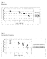
- Fig. 1 shows the changes in the deposition speed for each target throughout the target life. Needless to say, this data is the original deposition speed data which was not subject to functional program control on the device side.
- the X-ray intensity ratio of the ⁇ 110 ⁇ plane of the target bulk was in the range of 0.03 to 0.38, which is within the range of the present invention.
- the tendency was such that higher the degree of rolling process (%), lower the intensity ratio of the ⁇ 110 ⁇ plane.
- Variation of the deposition speed was in the range of 0.4 to 1.5nm/sec, and it is evident that higher the degree of rolling process (%), smaller the variation.
- Example 3 and Example 4 the X-ray intensity ratios of the ⁇ 110 ⁇ plane of the target bulk were in the range of 0.05 to 0.12 and 0.03 to 0.09, and were even lower in comparison to Example 1 and Example 2.
- the variations of the deposition speed in the foregoing case were 0.7nm/sec and 0.4nm/sec, and showed more favorable values.
- the X-ray intensity ratio of the ⁇ 110 ⁇ plane based on the X-ray diffraction of the target bulk is small at 0.2 or less, it is evident that more superior characteristics can be realized.
- Fig. 1 is an illustration of the above, and shows that the variation in the deposition speed was small. Further, as shown in Table 1, the functional control of the deposition speed was possible in all cases.
- Table 1 Composition Degree of Rolling Process (%) ⁇ 110 ⁇ Intensity Ratio Bulk ⁇ 110 ⁇ Intensity Ratio Surface ⁇ 110 ⁇ Intensity Ratio at Depth of Approx. 100 ⁇ ⁇ 110 ⁇ Intensity Ratio at Depth of Approx, 50 ⁇ ⁇ 110 ⁇ Intensity Ratio at Depth of Approx.
- an EB molten Ta ingot ( ⁇ 190 ⁇ 60mmh) having a purity level of 4N5 was subject to deformation processing and heat treatment and used as the raw material. Foremost, the ingot was subject to cold tightening and forging up to ⁇ 100 ⁇ 100mmh, and thereafter subject to upset forging up to ⁇ 160mm.
- cold rolling was performed up to a thickness of 10mm.
- the plane orientation was controlled by adjusting the degree of rolling process according to the thickness of the preform during upset forging.
- the degree of rolling process was as shown in Table 2.
- the ingot was subject to heat treatment for 2 hours at 1000°C, and then subject to machining process to be formed into a target shape.
- FIG. 2 shows the changes in the deposition speed for each target throughout the target life. Needless to say, this data is the original deposition speed data which was not subject to functional program control on the device side.
- the X-ray intensity ratio of the ⁇ 110 ⁇ plane of the target bulk was in the range of 0,45 to 0.60.
- the tendency was such that lower the degree of rolling process (%), higher the intensity ratio of the ⁇ 110 ⁇ plane, and all cases exceeded the conditions of the present invention.
- Variation of the deposition speed was in the range of 4.1 to 5.6nm/sec, and it is evident that higher the degree of rolling process (%), greater the variation, and these Comparative Examples could not achieve the objective of the present invention.
- Fig. 2 is an illustration of the above, and shows that the variation in the deposition speed is great. Further, as shown in Table 2, the functional control of the deposition speed was not possible in any of the cases.
- Table 2 Composition Degree of Rolling Process (%) ⁇ 110 ⁇ Intensity Ratio Bulk ⁇ 110 ⁇ Intensity Ratio Surface ⁇ 110 ⁇ Intensity Ratio at Depth of Approx. 100 ⁇ ⁇ 110 ⁇ Intensity Ratio at Depth of Approx. 50 ⁇ ⁇ 110 ⁇ Intensity Ratio at Depth of Approx.
- An EB molten Ta ingot ( ⁇ 190 ⁇ 60mmh) having a purity level of 4N5 was subject to deformation processing and heat treatment and used as the raw material. Foremost, the ingot was subject to cold tightening and forging up to ⁇ 100 ⁇ 100mmh, and thereafter subject to upset forging up to ⁇ 160mm.
- the ingot was subject to heat treatment for 2 hours at 1000°C, and then subject to machining process to be formed into a target shape.
- Certain targets were placed in a vacuum heat treatment furnace and subject to degassing heat treatment for 1 hour at 100°C, 150°C, and 200°C, and the warping of the target was thereby measured.
- Fig. 3 shows the changes in the deposition speed for each target throughout the target life. Needless to say, this data is the original deposition speed data which was not subject to functional program control on the device side. Fig. 3 shows the relation between the erosion depth and deposition speed of the target during the initial stages of sputtering.
- the X-ray intensity ratio of the ⁇ 110 ⁇ plane was in the range of 0.07 to 0.38.
- the tendency was such that higher the degree of rolling process (%), lower the intensity ratio of the ⁇ 110 ⁇ plane.
- Variation of the deposition speed was in the range of 4 to 23nm/sec, and it is evident that higher the degree of rolling process (%), smaller the variation.
- Table 3 Composition Degree of Rolling Process (%) ⁇ 110 ⁇ Intensity Ratio Bulk ⁇ 110 ⁇ Intensity Ratio Surface ⁇ 110 ⁇ Intensity Ratio at Depth of Approx. 100 ⁇ ⁇ 110 ⁇ Intensity Ratio at Depth of Approx. 50 ⁇ ⁇ 110 ⁇ Intensity Ratio at Depth of Approx.
- An EB molten Ta ingot ( ⁇ 190 ⁇ 60mmh) having a purity level of 4N5 was subject to deformation processing and heat treatment and used as the raw material. Foremost, the ingot was subject to cold tightening and forging up to ⁇ 100 ⁇ 100mmh, and thereafter subject to upset forging up to ⁇ 160mm.
- the ingot was subject to heat treatment for 2 hours at 1000°C, and then subject to machining process to be formed into a target shape.
- Certain targets were placed in a vacuum heat treatment furnace and subject to degassing heat treatment for 1 hour at 100°C, 150°C, and 200°C.
- Fig. 4 shows the changes in the deposition speed for each target throughout the target life. Needless to say, this data is the original deposition speed data which was not subject to functional program control on the device side. Fig. 4 shows the relation between the erosion depth and deposition speed of the target during the initial stages of sputtering.
- the X-ray intensity ratio of the ⁇ 110 ⁇ plane of the target bulk was in the range of 0.45 to 0.59.
- the tendency was such that higher the degree of rolling process (%), lower the intensity ratio of the ⁇ 110 ⁇ plane.
- Variation of the deposition speed was in the range of 37 to 40nm/sec, and it is evident that higher the degree of rolling process (%), smaller the variation.
- Table 4 Composition Degree of Rolling Process (%) ⁇ 110 ⁇ Intensity Ratio Bulk ⁇ 110 ⁇ Intensity Ratio Surface ⁇ 110 ⁇ Intensity Ratio at Depth of Approx. 100 ⁇ ⁇ 110 ⁇ Intensity Ratio at Depth of Approx. 50 ⁇ ⁇ 110 ⁇ Intensity Ratio at Depth of Approx.
- a Ta-5wt% Mo EB molten ingot ( ⁇ 190 ⁇ 60mmh) having a purity level of 4N5 was subject to deformation processing and heat treatment and used as the raw material. Foremost, the ingot was subject to cold tightening and forging up to ⁇ 100 ⁇ 100mmh, and thereafter subject to upset forging up to ⁇ 160mm.
- the ingot was subject to heat treatment for 2 hours at 1000°C, and then subject to machining process to be formed into a target shape.
- Table 5 and Fig. 5 summarize the data of Examples 10 and 11.
- Fig. 5 shows the changes in the deposition speed for each target throughout the target life. Needless to say, this data is the original deposition speed data which was not subject to functional program control on the device side.
- the X-ray intensity ratio of the ⁇ 110 ⁇ plane of the target bulk was in the range of 0.05 to 0.37.
- the tendency was such that higher the degree of rolling process (%), lower the intensity ratio of the ⁇ 110 ⁇ plane.
- Variation of the deposition speed was in the range of 1.1 to 1.6nm/sec, and it is evident that higher the degree of rolling process (%), smaller the variation.
- Example 11 the X-ray intensity ratio of the ⁇ 110 ⁇ plane was 0.2 or less, and this case showed characteristic values that were even more favorable than Example 10.
- Example 3 show the same tendency as Example 3 and Example 4.
- the X-ray diffraction intensity ratio of the ⁇ 110 ⁇ plane was made to be 0.2 or less, it was possible to effectively inhibit variation in the deposition speed even further.
- Table 5 Composition Degree of Rolling Process (%) ⁇ 110 ⁇ Intensity Ratio Bulk ⁇ 110 ⁇ Intensity Ratio Surface ⁇ 110 ⁇ Intensity Ratio at Depth of Approx.100 ⁇ ⁇ 110 ⁇ Intensity Ratio at Depth of Approx. 50 ⁇ ⁇ 110 ⁇ Intensity Ratio at Depth of Approx.
- a Ta-5wt% Mo EB molten ingot ( ⁇ 190 ⁇ 60mmh) having a purity level of 4N5 was subject to deformation processing and heat treatment and used as the raw material. Foremost, the ingot was subject to cold tightening and forging up to ⁇ 100 ⁇ 100mmh, and thereafter subject to upset forging up to ⁇ 160mm.
- the ingot was subject to heat treatment for 2 hours at 1000°C, and then subject to machining process to be formed into a target shape.
- Table 6 and Fig. 6 summarize the data of Comparative Examples 6 and 7.
- Fig. 6 shows the changes in the deposition speed for each target throughout the target life. Needless to say, this data is the original deposition speed data which was not subject to functional program control on the device side.
- the X-ray intensity ratio of the ⁇ 110 ⁇ plane of the target bulk was in the range of 0.43 to 0.66, and all cases exceeded the conditions of the present invention.
- Variation of the deposition speed was in the range of 4.6 to 6.6nm/sec, and it is evident that higher the degree of rolling process (%), greater the variation, and these Comparative Examples could not achieve the objective of the present invention.
- Fig. 6 is an illustration of the above, and shows that the variation in the deposition speed is great. Further, as shown in Table 6, the functional control of the deposition speed was not possible in any of the cases.
- Table 6 Composition Degree of Rolling Process (%) ⁇ 110 ⁇ Intensity Ratio Bulk ⁇ 110 ⁇ Intensity Ratio Surface ⁇ 110 ⁇ Intensity Ratio at Depth of Approx. 100 ⁇ ⁇ 110 ⁇ Intensity Ratio at Depth of Approx. 50 ⁇ ⁇ 110 ⁇ Intensity Ratio at Depth of Approx.
- the Examples of the present invention only show the X-ray intensity ratio of the ⁇ 110 ⁇ plane as the bulk material regarding the tantalum alloy (Ta-Mo alloy), the results were the same as Examples 5 to 9. Further, based on the results of the foregoing tantalum and tantalum alloy (Ta-Mo alloy), it is evident that the other tantalum alloys having tantalum as its primary component such as alloy systems of compositions in which the crystal structure of Ta-W, Ta-Nb, Ta-Hf, Ta-Ti or the like is not significantly different from pure Ta will also achieve the same results as the Examples and Comparative Examples, and these are also covered by the present invention as a matter of course.
- the present invention yields a superior effect of being able to minimize the fluctuation of the deposition speed for each target throughout the target life, and thereby improve and stabilize the production efficiency of semiconductors during the sputtering process, and contribute to the significant reduction of production costs.
- the present invention is extremely useful as a tantalum or tantalum alloy target.
Landscapes
- Chemical & Material Sciences (AREA)
- Engineering & Computer Science (AREA)
- Materials Engineering (AREA)
- Mechanical Engineering (AREA)
- Metallurgy (AREA)
- Organic Chemistry (AREA)
- Chemical Kinetics & Catalysis (AREA)
- Physical Vapour Deposition (AREA)
Applications Claiming Priority (2)
| Application Number | Priority Date | Filing Date | Title |
|---|---|---|---|
| JP2005132224 | 2005-04-28 | ||
| PCT/JP2006/306223 WO2006117949A1 (ja) | 2005-04-28 | 2006-03-28 | スパッタリングターゲット |
Publications (2)
| Publication Number | Publication Date |
|---|---|
| EP1876258A1 true EP1876258A1 (de) | 2008-01-09 |
| EP1876258A4 EP1876258A4 (de) | 2008-08-13 |
Family
ID=37307755
Family Applications (1)
| Application Number | Title | Priority Date | Filing Date |
|---|---|---|---|
| EP06730171A Ceased EP1876258A4 (de) | 2005-04-28 | 2006-03-28 | Sputtertarget |
Country Status (7)
| Country | Link |
|---|---|
| US (1) | US8177947B2 (de) |
| EP (1) | EP1876258A4 (de) |
| JP (1) | JP5126742B2 (de) |
| KR (1) | KR100968395B1 (de) |
| CN (1) | CN101171362B (de) |
| TW (1) | TW200704799A (de) |
| WO (1) | WO2006117949A1 (de) |
Families Citing this family (14)
| Publication number | Priority date | Publication date | Assignee | Title |
|---|---|---|---|---|
| US8252126B2 (en) * | 2004-05-06 | 2012-08-28 | Global Advanced Metals, Usa, Inc. | Sputter targets and methods of forming same by rotary axial forging |
| EP1942204B1 (de) * | 2005-10-04 | 2012-04-25 | JX Nippon Mining & Metals Corporation | Sputtertarget |
| JP4879986B2 (ja) * | 2006-06-29 | 2012-02-22 | Jx日鉱日石金属株式会社 | スパッタリングターゲット/バッキングプレート接合体 |
| KR101288651B1 (ko) | 2009-05-22 | 2013-07-22 | 제이엑스 닛코 닛세키 킨조쿠 가부시키가이샤 | 탄탈륨 스퍼터링 타겟 |
| KR101338758B1 (ko) | 2009-08-11 | 2013-12-06 | 제이엑스 닛코 닛세키 킨조쿠 가부시키가이샤 | 탄탈륨 스퍼터링 타깃 |
| KR101944580B1 (ko) | 2010-08-09 | 2019-01-31 | 제이엑스금속주식회사 | 탄탈 스퍼터링 타깃 |
| KR101927574B1 (ko) | 2012-12-19 | 2018-12-10 | 제이엑스금속주식회사 | 탄탈 스퍼터링 타깃 및 그 제조 방법 |
| CN105431565B (zh) | 2012-12-19 | 2018-06-05 | 吉坤日矿日石金属株式会社 | 钽溅射靶及其制造方法 |
| WO2014136679A1 (ja) | 2013-03-04 | 2014-09-12 | Jx日鉱日石金属株式会社 | タンタルスパッタリングターゲット及びその製造方法 |
| KR20160052664A (ko) | 2013-10-01 | 2016-05-12 | 제이엑스 킨조쿠 가부시키가이샤 | 탄탈 스퍼터링 타깃 |
| KR102074047B1 (ko) | 2015-05-22 | 2020-02-05 | 제이엑스금속주식회사 | 탄탈 스퍼터링 타깃 및 그 제조 방법 |
| CN107109634B (zh) | 2015-05-22 | 2020-08-28 | 捷客斯金属株式会社 | 钽溅射靶及其制造方法 |
| US9546837B1 (en) | 2015-10-09 | 2017-01-17 | Bh5773 Ltd | Advanced gun barrel |
| CN109154074B (zh) | 2017-03-30 | 2020-11-24 | Jx金属株式会社 | 钽溅射靶 |
Citations (2)
| Publication number | Priority date | Publication date | Assignee | Title |
|---|---|---|---|---|
| US20020026965A1 (en) * | 1998-11-25 | 2002-03-07 | Michaluk Christopher A. | High purity tantalum, products containing the same, and methods of making the same |
| WO2003025238A1 (en) * | 2001-09-18 | 2003-03-27 | Praxair S. T. Technology, Inc. | Textured-grain-powder metallurgy tantalum sputter target |
Family Cites Families (14)
| Publication number | Priority date | Publication date | Assignee | Title |
|---|---|---|---|---|
| DE3825634C2 (de) * | 1988-07-28 | 1994-06-30 | Thyssen Stahl Ag | Verfahren zur Erzeugung von Warmbad oder Grobblechen |
| US6197134B1 (en) * | 1997-01-08 | 2001-03-06 | Dowa Mining Co., Ltd. | Processes for producing fcc metals |
| JPH1180942A (ja) | 1997-09-10 | 1999-03-26 | Japan Energy Corp | Taスパッタターゲットとその製造方法及び組立体 |
| US6323055B1 (en) * | 1998-05-27 | 2001-11-27 | The Alta Group, Inc. | Tantalum sputtering target and method of manufacture |
| US6348139B1 (en) * | 1998-06-17 | 2002-02-19 | Honeywell International Inc. | Tantalum-comprising articles |
| US6193821B1 (en) * | 1998-08-19 | 2001-02-27 | Tosoh Smd, Inc. | Fine grain tantalum sputtering target and fabrication process |
| US6331233B1 (en) * | 2000-02-02 | 2001-12-18 | Honeywell International Inc. | Tantalum sputtering target with fine grains and uniform texture and method of manufacture |
| EP1287172B1 (de) * | 2000-05-22 | 2008-10-29 | Cabot Corporation | Hochreines niobmetall und erzeugnisse daraus und verfahren zu dessen herstellung |
| JP3905301B2 (ja) * | 2000-10-31 | 2007-04-18 | 日鉱金属株式会社 | タンタル又はタングステンターゲット−銅合金製バッキングプレート組立体及びその製造方法 |
| JP4883546B2 (ja) * | 2002-09-20 | 2012-02-22 | Jx日鉱日石金属株式会社 | タンタルスパッタリングターゲットの製造方法 |
| JP4263900B2 (ja) * | 2002-11-13 | 2009-05-13 | 日鉱金属株式会社 | Taスパッタリングターゲット及びその製造方法 |
| US8172960B2 (en) * | 2003-04-01 | 2012-05-08 | Jx Nippon Mining & Metals Corporation | Tantalum sputtering target and method of manufacturing same |
| EP1681368B1 (de) * | 2003-11-06 | 2021-06-30 | JX Nippon Mining & Metals Corporation | Tantal-sputtertarget herstellungsverfahren |
| US8252126B2 (en) * | 2004-05-06 | 2012-08-28 | Global Advanced Metals, Usa, Inc. | Sputter targets and methods of forming same by rotary axial forging |
-
2006
- 2006-03-28 CN CN2006800147921A patent/CN101171362B/zh active Active
- 2006-03-28 JP JP2007514508A patent/JP5126742B2/ja active Active
- 2006-03-28 EP EP06730171A patent/EP1876258A4/de not_active Ceased
- 2006-03-28 WO PCT/JP2006/306223 patent/WO2006117949A1/ja active Application Filing
- 2006-03-28 US US11/912,450 patent/US8177947B2/en active Active
- 2006-03-28 KR KR1020077024857A patent/KR100968395B1/ko active IP Right Grant
- 2006-04-03 TW TW095111746A patent/TW200704799A/zh unknown
Patent Citations (2)
| Publication number | Priority date | Publication date | Assignee | Title |
|---|---|---|---|---|
| US20020026965A1 (en) * | 1998-11-25 | 2002-03-07 | Michaluk Christopher A. | High purity tantalum, products containing the same, and methods of making the same |
| WO2003025238A1 (en) * | 2001-09-18 | 2003-03-27 | Praxair S. T. Technology, Inc. | Textured-grain-powder metallurgy tantalum sputter target |
Non-Patent Citations (3)
| Title |
|---|
| DATABASE COMPENDEX [Online] ENGINEERING INFORMATION, INC., NEW YORK, NY, US; WICKERSHAM CHARLES E ET AL: "Tantalum angular sputter emission distributions" XP002486593 Database accession no. E2005179064023 & JOM; JOM NOVEMBER 2004, vol. 56, no. 11, November 2004 (2004-11), page 210, * |
| JIANG A ET AL: "Investigation of the structure of beta-tantalum", THIN SOLID FILMS, ELSEVIER-SEQUOIA S.A. LAUSANNE, CH, vol. 437, no. 1-2, 1 August 2003 (2003-08-01), pages 116-122, XP004438583, ISSN: 0040-6090, DOI: 10.1016/S0040-6090(03)00702-8 * |
| See also references of WO2006117949A1 * |
Also Published As
| Publication number | Publication date |
|---|---|
| WO2006117949A1 (ja) | 2006-11-09 |
| TWI326716B (de) | 2010-07-01 |
| US8177947B2 (en) | 2012-05-15 |
| EP1876258A4 (de) | 2008-08-13 |
| JP5126742B2 (ja) | 2013-01-23 |
| JPWO2006117949A1 (ja) | 2008-12-18 |
| CN101171362B (zh) | 2010-06-09 |
| CN101171362A (zh) | 2008-04-30 |
| TW200704799A (en) | 2007-02-01 |
| US20090032392A1 (en) | 2009-02-05 |
| KR20070121025A (ko) | 2007-12-26 |
| KR100968395B1 (ko) | 2010-07-07 |
Similar Documents
| Publication | Publication Date | Title |
|---|---|---|
| EP1876258A1 (de) | Sputtertarget | |
| US6331233B1 (en) | Tantalum sputtering target with fine grains and uniform texture and method of manufacture | |
| US9859104B2 (en) | Tantalum sputtering target and production method therefor | |
| EP2418299A1 (de) | Tantalum-sputtertarget | |
| US20160208377A1 (en) | Tantalum sputtering target and method for producing same | |
| US20220162743A1 (en) | Titanium Sputtering Target, Production Method Therefor, And Method For Producing Titanium-Containing Thin Film | |
| US10407766B2 (en) | Tantalum sputtering target and method for producing same | |
| EP2878699A1 (de) | Tantalsputtertarget und herstellungsverfahren dafür | |
| CN110129744B (zh) | 溅射用钛靶 | |
| EP2634287B1 (de) | Titan-sputtertarget | |
| JP6293929B2 (ja) | タンタルスパッタリングターゲット及びその製造方法 | |
| JP6293928B2 (ja) | タンタルスパッタリングターゲット及びその製造方法 | |
| US11837449B2 (en) | Ti-Nb alloy sputtering target and production method thereof | |
| US7517417B2 (en) | Tantalum PVD component producing methods | |
| WO2014156918A1 (ja) | ニオブスパッタリングターゲット |
Legal Events
| Date | Code | Title | Description |
|---|---|---|---|
| PUAI | Public reference made under article 153(3) epc to a published international application that has entered the european phase |
Free format text: ORIGINAL CODE: 0009012 |
|
| 17P | Request for examination filed |
Effective date: 20071026 |
|
| AK | Designated contracting states |
Kind code of ref document: A1 Designated state(s): DE FR |
|
| DAX | Request for extension of the european patent (deleted) | ||
| RBV | Designated contracting states (corrected) |
Designated state(s): DE FR |
|
| A4 | Supplementary search report drawn up and despatched |
Effective date: 20080715 |
|
| 17Q | First examination report despatched |
Effective date: 20090121 |
|
| RAP1 | Party data changed (applicant data changed or rights of an application transferred) |
Owner name: JX NIPPON MINING & METALS CORPORATION |
|
| APBK | Appeal reference recorded |
Free format text: ORIGINAL CODE: EPIDOSNREFNE |
|
| APBN | Date of receipt of notice of appeal recorded |
Free format text: ORIGINAL CODE: EPIDOSNNOA2E |
|
| APBR | Date of receipt of statement of grounds of appeal recorded |
Free format text: ORIGINAL CODE: EPIDOSNNOA3E |
|
| APAV | Appeal reference deleted |
Free format text: ORIGINAL CODE: EPIDOSDREFNE |
|
| REG | Reference to a national code |
Ref country code: DE Ref legal event code: R003 |
|
| APBT | Appeal procedure closed |
Free format text: ORIGINAL CODE: EPIDOSNNOA9E |
|
| STAA | Information on the status of an ep patent application or granted ep patent |
Free format text: STATUS: THE APPLICATION HAS BEEN REFUSED |
|
| 18R | Application refused |
Effective date: 20150427 |