EP1873839A2 - Semiconductor device - Google Patents
Semiconductor device Download PDFInfo
- Publication number
- EP1873839A2 EP1873839A2 EP07012590A EP07012590A EP1873839A2 EP 1873839 A2 EP1873839 A2 EP 1873839A2 EP 07012590 A EP07012590 A EP 07012590A EP 07012590 A EP07012590 A EP 07012590A EP 1873839 A2 EP1873839 A2 EP 1873839A2
- Authority
- EP
- European Patent Office
- Prior art keywords
- region
- semiconductor
- buried
- layer
- type
- Prior art date
- Legal status (The legal status is an assumption and is not a legal conclusion. Google has not performed a legal analysis and makes no representation as to the accuracy of the status listed.)
- Withdrawn
Links
Images





Classifications
-
- H—ELECTRICITY
- H10—SEMICONDUCTOR DEVICES; ELECTRIC SOLID-STATE DEVICES NOT OTHERWISE PROVIDED FOR
- H10D—INORGANIC ELECTRIC SEMICONDUCTOR DEVICES
- H10D30/00—Field-effect transistors [FET]
- H10D30/01—Manufacture or treatment
- H10D30/021—Manufacture or treatment of FETs having insulated gates [IGFET]
- H10D30/028—Manufacture or treatment of FETs having insulated gates [IGFET] of double-diffused metal oxide semiconductor [DMOS] FETs
- H10D30/0291—Manufacture or treatment of FETs having insulated gates [IGFET] of double-diffused metal oxide semiconductor [DMOS] FETs of vertical DMOS [VDMOS] FETs
-
- H—ELECTRICITY
- H10—SEMICONDUCTOR DEVICES; ELECTRIC SOLID-STATE DEVICES NOT OTHERWISE PROVIDED FOR
- H10D—INORGANIC ELECTRIC SEMICONDUCTOR DEVICES
- H10D12/00—Bipolar devices controlled by the field effect, e.g. insulated-gate bipolar transistors [IGBT]
- H10D12/01—Manufacture or treatment
- H10D12/031—Manufacture or treatment of IGBTs
-
- H—ELECTRICITY
- H10—SEMICONDUCTOR DEVICES; ELECTRIC SOLID-STATE DEVICES NOT OTHERWISE PROVIDED FOR
- H10D—INORGANIC ELECTRIC SEMICONDUCTOR DEVICES
- H10D12/00—Bipolar devices controlled by the field effect, e.g. insulated-gate bipolar transistors [IGBT]
- H10D12/01—Manufacture or treatment
- H10D12/031—Manufacture or treatment of IGBTs
- H10D12/032—Manufacture or treatment of IGBTs of vertical IGBTs
-
- H—ELECTRICITY
- H10—SEMICONDUCTOR DEVICES; ELECTRIC SOLID-STATE DEVICES NOT OTHERWISE PROVIDED FOR
- H10D—INORGANIC ELECTRIC SEMICONDUCTOR DEVICES
- H10D12/00—Bipolar devices controlled by the field effect, e.g. insulated-gate bipolar transistors [IGBT]
- H10D12/411—Insulated-gate bipolar transistors [IGBT]
- H10D12/441—Vertical IGBTs
-
- H—ELECTRICITY
- H10—SEMICONDUCTOR DEVICES; ELECTRIC SOLID-STATE DEVICES NOT OTHERWISE PROVIDED FOR
- H10D—INORGANIC ELECTRIC SEMICONDUCTOR DEVICES
- H10D30/00—Field-effect transistors [FET]
- H10D30/60—Insulated-gate field-effect transistors [IGFET]
- H10D30/64—Double-diffused metal-oxide semiconductor [DMOS] FETs
- H10D30/66—Vertical DMOS [VDMOS] FETs
- H10D30/665—Vertical DMOS [VDMOS] FETs having edge termination structures
-
- H—ELECTRICITY
- H10—SEMICONDUCTOR DEVICES; ELECTRIC SOLID-STATE DEVICES NOT OTHERWISE PROVIDED FOR
- H10D—INORGANIC ELECTRIC SEMICONDUCTOR DEVICES
- H10D62/00—Semiconductor bodies, or regions thereof, of devices having potential barriers
- H10D62/10—Shapes, relative sizes or dispositions of the regions of the semiconductor bodies; Shapes of the semiconductor bodies
- H10D62/102—Constructional design considerations for preventing surface leakage or controlling electric field concentration
- H10D62/103—Constructional design considerations for preventing surface leakage or controlling electric field concentration for increasing or controlling the breakdown voltage of reverse-biased devices
- H10D62/105—Constructional design considerations for preventing surface leakage or controlling electric field concentration for increasing or controlling the breakdown voltage of reverse-biased devices by having particular doping profiles, shapes or arrangements of PN junctions; by having supplementary regions, e.g. junction termination extension [JTE]
- H10D62/106—Constructional design considerations for preventing surface leakage or controlling electric field concentration for increasing or controlling the breakdown voltage of reverse-biased devices by having particular doping profiles, shapes or arrangements of PN junctions; by having supplementary regions, e.g. junction termination extension [JTE] having supplementary regions doped oppositely to or in rectifying contact with regions of the semiconductor bodies, e.g. guard rings with PN or Schottky junctions
- H10D62/107—Buried supplementary regions, e.g. buried guard rings
-
- H—ELECTRICITY
- H10—SEMICONDUCTOR DEVICES; ELECTRIC SOLID-STATE DEVICES NOT OTHERWISE PROVIDED FOR
- H10D—INORGANIC ELECTRIC SEMICONDUCTOR DEVICES
- H10D62/00—Semiconductor bodies, or regions thereof, of devices having potential barriers
- H10D62/10—Shapes, relative sizes or dispositions of the regions of the semiconductor bodies; Shapes of the semiconductor bodies
- H10D62/102—Constructional design considerations for preventing surface leakage or controlling electric field concentration
- H10D62/103—Constructional design considerations for preventing surface leakage or controlling electric field concentration for increasing or controlling the breakdown voltage of reverse-biased devices
- H10D62/105—Constructional design considerations for preventing surface leakage or controlling electric field concentration for increasing or controlling the breakdown voltage of reverse-biased devices by having particular doping profiles, shapes or arrangements of PN junctions; by having supplementary regions, e.g. junction termination extension [JTE]
- H10D62/109—Reduced surface field [RESURF] PN junction structures
- H10D62/111—Multiple RESURF structures, e.g. double RESURF or 3D-RESURF structures
-
- H—ELECTRICITY
- H10—SEMICONDUCTOR DEVICES; ELECTRIC SOLID-STATE DEVICES NOT OTHERWISE PROVIDED FOR
- H10D—INORGANIC ELECTRIC SEMICONDUCTOR DEVICES
- H10D62/00—Semiconductor bodies, or regions thereof, of devices having potential barriers
- H10D62/80—Semiconductor bodies, or regions thereof, of devices having potential barriers characterised by the materials
- H10D62/83—Semiconductor bodies, or regions thereof, of devices having potential barriers characterised by the materials being Group IV materials, e.g. B-doped Si or undoped Ge
- H10D62/832—Semiconductor bodies, or regions thereof, of devices having potential barriers characterised by the materials being Group IV materials, e.g. B-doped Si or undoped Ge being Group IV materials comprising two or more elements, e.g. SiGe
- H10D62/8325—Silicon carbide
-
- H—ELECTRICITY
- H10—SEMICONDUCTOR DEVICES; ELECTRIC SOLID-STATE DEVICES NOT OTHERWISE PROVIDED FOR
- H10D—INORGANIC ELECTRIC SEMICONDUCTOR DEVICES
- H10D8/00—Diodes
- H10D8/01—Manufacture or treatment
- H10D8/051—Manufacture or treatment of Schottky diodes
-
- H—ELECTRICITY
- H10—SEMICONDUCTOR DEVICES; ELECTRIC SOLID-STATE DEVICES NOT OTHERWISE PROVIDED FOR
- H10D—INORGANIC ELECTRIC SEMICONDUCTOR DEVICES
- H10D8/00—Diodes
- H10D8/411—PN diodes having planar bodies
-
- H—ELECTRICITY
- H10—SEMICONDUCTOR DEVICES; ELECTRIC SOLID-STATE DEVICES NOT OTHERWISE PROVIDED FOR
- H10D—INORGANIC ELECTRIC SEMICONDUCTOR DEVICES
- H10D8/00—Diodes
- H10D8/60—Schottky-barrier diodes
-
- H—ELECTRICITY
- H10—SEMICONDUCTOR DEVICES; ELECTRIC SOLID-STATE DEVICES NOT OTHERWISE PROVIDED FOR
- H10D—INORGANIC ELECTRIC SEMICONDUCTOR DEVICES
- H10D62/00—Semiconductor bodies, or regions thereof, of devices having potential barriers
- H10D62/10—Shapes, relative sizes or dispositions of the regions of the semiconductor bodies; Shapes of the semiconductor bodies
- H10D62/102—Constructional design considerations for preventing surface leakage or controlling electric field concentration
- H10D62/103—Constructional design considerations for preventing surface leakage or controlling electric field concentration for increasing or controlling the breakdown voltage of reverse-biased devices
- H10D62/105—Constructional design considerations for preventing surface leakage or controlling electric field concentration for increasing or controlling the breakdown voltage of reverse-biased devices by having particular doping profiles, shapes or arrangements of PN junctions; by having supplementary regions, e.g. junction termination extension [JTE]
-
- H—ELECTRICITY
- H10—SEMICONDUCTOR DEVICES; ELECTRIC SOLID-STATE DEVICES NOT OTHERWISE PROVIDED FOR
- H10D—INORGANIC ELECTRIC SEMICONDUCTOR DEVICES
- H10D62/00—Semiconductor bodies, or regions thereof, of devices having potential barriers
- H10D62/10—Shapes, relative sizes or dispositions of the regions of the semiconductor bodies; Shapes of the semiconductor bodies
- H10D62/102—Constructional design considerations for preventing surface leakage or controlling electric field concentration
- H10D62/103—Constructional design considerations for preventing surface leakage or controlling electric field concentration for increasing or controlling the breakdown voltage of reverse-biased devices
- H10D62/105—Constructional design considerations for preventing surface leakage or controlling electric field concentration for increasing or controlling the breakdown voltage of reverse-biased devices by having particular doping profiles, shapes or arrangements of PN junctions; by having supplementary regions, e.g. junction termination extension [JTE]
- H10D62/106—Constructional design considerations for preventing surface leakage or controlling electric field concentration for increasing or controlling the breakdown voltage of reverse-biased devices by having particular doping profiles, shapes or arrangements of PN junctions; by having supplementary regions, e.g. junction termination extension [JTE] having supplementary regions doped oppositely to or in rectifying contact with regions of the semiconductor bodies, e.g. guard rings with PN or Schottky junctions
-
- H—ELECTRICITY
- H10—SEMICONDUCTOR DEVICES; ELECTRIC SOLID-STATE DEVICES NOT OTHERWISE PROVIDED FOR
- H10D—INORGANIC ELECTRIC SEMICONDUCTOR DEVICES
- H10D64/00—Electrodes of devices having potential barriers
- H10D64/111—Field plates
Definitions
- the present invention relates to a high-voltage semiconductor device which develops a stable breakdown voltage characteristic.
- a high-voltage diode and a MOSFET have been used as a semiconductor device for electric power control.
- Such a kind of semiconductor device has been required to improve conflicting characteristics, such as, an improvement in breakdown voltage and a reduction in on-state resistance, and a variety of proposals on this requirement have been offered.
- JP-A H9-191109 discloses a technique which disposes a plurality of stripe-shape p-type buried layers near by the surface of an n-type base layer of a Schottky barrier diode (FIG. 12 of the patent document).
- This p-type buried layer is designed such that a depletion layer from a Schottky interface reaches the p-type buried layer before the electric field at the Schottky interface reaches maximum electric field of the semiconductor surface.
- the depletion layer reaches the p-type buried layer, the largest point of the electric field at the Schottky interface is fixed not to be raised, and the depletion layer newly spreads onto an ohmic electrode side from the buried layer.
- the voltage held by the epitaxial layer between the Schottky interface and the buried layer is set to a value lower than the maximum blocking (breakdown) voltage. Thereby, the electric field at the Schottky interface is fixed to a low value, and the leakage current from the Schottky interface may be decreased.
- the technique disclosed in the aforementioned patent document disposes a plurality of stages of p-type buried layers as depicted in FIG. 13 of said patent document, shares a breakdown voltage by means of n-type base layers divided by the plurality of stages of p-type buried layers, and develops a Schottky barrier diode which achieves a small voltage drop when conducting at a high voltage.
- the forgoing conventional improvement is specified only for an active region under an anode electrode, and it does not take so much account to an n-type base layer under an edge termination structure.
- a planer-type high-voltage device though it has high-voltage performance based on the p-type layer buried in the active region, it poses the problem that the breakdown voltage is determined by an electric field concentration at an edge termination region. If the edge termination structure is microscopic like guard rings, and when widths and intervals of the patterns vary due to a mask misalignment, the problem of lowering in breakdown voltage occurs.
- planer device has many advantages for mass production on those points which are more stable in process, and are higher in yield ration and in throughput than a mesa-type device. Therefore, it has been desired to attain a high-breakdown-voltage device having a planar structure stable in breakdown voltage.
- a semiconductor device which includes:
- a semiconductor device of the present invention described in the following embodiments is provided with a second semiconductor region of a second conductivity type buried in a sheet shape or a mesh shape in an edge termination region of a semiconductor layer of a first conductivity type substantially in parallel with the surface of the semiconductor layer.
- a reverse voltage is applied between a first electrode and a second electrode, equipotential surfaces formed on upper parts of the semiconductor layer being bent toward a direction along the surface of the second semiconductor region so as to be converged with each other.
- the semiconductor device is hard to be broken at the edge termination region and has a stable breakdown voltage characteristic.
- FIG. 1 is a longitudinal sectional view of one element of a semiconductor device (vertical Schottky barrier diode) according to the first embodiment.
- FIG. 2 illustrates a schematic transverse sectional view along a II-II line of FIG. 1, and constituent components of one element of the embodiment are formed in a concentric circle shape in a plane except a component of reference number 5.
- the constituent components may be modified and formed such that components of reference numbers 5 and 7 are made as rectangular rings each with a round (R) at its corners for releasing an electric field concentration.
- n-type SiC semiconductor layer 2 is formed on a highly doped n + -type SiC semiconductor substrate 1.
- a RESURF layer 8 containing p-type impurities is formed in an annular shape so as to surround an active region A at a surface central part of the SiC semiconductor layer 2. If further high-breakdown voltage is required, it is preferable to form an edge termination layer (not shown) containing p + type impurities inside the RESURF layer 8 so as to lie under an anode electrode edge.
- P-type guard rings 9 are formed so as to surround the RESURF layer 8 of p-type in order to further enhance the breakdown voltage.
- the guard rings 9 of p-type may further enhance effect by disposing a plurality thereof.
- the sameness of the impurity concentration in the RESURF layer 8 and the guard rings 9 makes easy in a manufacturing process, however it may be different from one another.
- the semiconductor device may include either the RESURF layer 8 or the guard rings 9.
- the surface of the active region surrounded by the RESURF layer 8 is provided with a first electrode 3 so as to be contacted with the surface.
- the first electrode 3 forms a Schottky junction with the SiC semiconductor layer 2, and uses, for example, Ti as a material.
- a pad electrode (or a field plate) 11 electrically connected to the first electrode 3 is formed thereon by, for example, Al.
- the pad electrode (field plate) 11 is formed also above the edge termination structure of the SiC semiconductor layer 2 with the RESURF layer 8 or the guard rings 9 formed thereon through a field-plate insulating film 12.
- the electric field being apt to concentrate to the edge part of the field plate 11 when the reverse electric field is applied thereto, it is preferable to be structured such that the edge part is disposed on the upper part of the RESIRF layer 8 or the guard rings 9.
- a second electrode 4 is formed on the bottom face of the SiC semiconductor substrate 1 by, for instance, Ni.
- p-type semiconductor regions 5 and 7 are buried inside the n-type SiC semiconductor layer 2 in order to be formed in a low-loss structure, namely in a high-breakdown voltage and low on-state resistance structure.
- a p-type region 5 having a plurality of openings is formed in order to have a high breakdown voltage structure and to secure a current path in the active region at the central part of the semiconductor device.
- the p-type region 7 is disposed in an electrically continued manner up to a device periphery on the outside of the active region.
- the periphery of the surface of the n-type semiconductor layer 2 is provided with an edge termination region 10 of a highly doped n + -type semiconductor.
- the depletion layer spreads in the device in the direction toward a second electrode through a Schottky interface, and also it spreads in the direction toward the RESURF layer 8 and the guard rings 9, namely in a lateral direction of the device.
- the depletion layer extended in the lateral direction spreads in the lateral direction while being pinned by the RESURF layer 8 and the guard rings 9.
- the depletion layer reaches the p-type buried regions 5 and 7.
- the electric field distributes on the buried p-type region 5 only two-dimensionally; however the depletion layer spreads toward the p-type region 7 three-dimensionally.
- the electric field on the semiconductor surface should be kept lower than the maximum electric field intensity, and also the depletion layer should not be spread up to the second electrode.
- the equipotential surface spreading in an oblique direction may be bent in a direction further parallel to the surface of the buried region 7, that is, may be bent so as to be converged along with the surface of the buried region 7.
- the buried region 7 like this does not exist, or on such a device in FIG. 4 in which the buried regions 5 at the center are formed to extend to the periphery thereof, all of the equipotential surfaces cannot be converged along the surface of the buried regions 5 because gaps (openings) are present in the buried regions 5 at the periphery thereof.
- the depletion layer does not reach the second electrode and a device with a further high breakdown voltage may be achieved. It is preferable for the aforementioned device to be designed such that the maximum electric field intensity becomes larger than the electric field with respect to the p-type buried regions 5 and 7.
- the longitudinal sectional view of the semiconductor of the embodiment is a symmetrical shape capable of being folded at a center line of each of FIGS. 5 to 8, so that only a right half thereof will be illustrated hereinafter to simplify FIGS. 5 to 8.
- the method forms a film of the n-type SiC layer 2 on the n + SiC semiconductor substrate 1 by epitaxial growth.
- the impurity concentration of the n-type SiC substrate 1 is, for example, 3 ⁇ 10 15 to 3 ⁇ 10 16 /cm 3 inclusive, and the present embodiment takes the case of the concentration of 1 ⁇ 10 16 /cm 3 as an example.
- the thickness of the SiC semiconductor layer 2 ranges from several ⁇ m to several dozen ⁇ m, and this embodiment sets it to 10 ⁇ m.
- the method forms the buried layer 5 under the active region and the buried layer 7 for burying the edge termination region simultaneously.
- a mask material onto the surface of the SiC semiconductor layer 1 to perform patterning forms desired mask patterns (not shown) of the p-type buried regions 5 and 7.
- the mask material uses a resist, a silicon oxide, a silicon nitride, a metal, etc.
- the method implants ions of p-type impurities through multi-level implantation from the upper surface of the mask material to form the p-type buried regions 5 and 7.
- p-type ion species aluminum (Al), boron (B), etc., are usually used; however in the embodiment, Al suitable for a fine pattern is used.
- ion accelerating energy energy of several keV to several hundred keV is usually used, and in the embodiment, the method uses the ion accelerating energy of 100-360 keV.
- An ion dose is set to its optimum value by a designed breakdown voltage and an epitaxial concentration, and the method performs Al multi-level ion implantation through the energy of, for example, from 100 to 360 keV inclusive with a dose ranging from 1 ⁇ 10 13 to 1 ⁇ 10 14 /cm 2 inclusive.
- the method may form a p-type well having a concentration ranging from 1 ⁇ 10 17 to 5 ⁇ 10 18 /cm 3 inclusive.
- both concentrations may be different from each other. If the concentrations are different from each other, after forming the mask of only the p-type buried region 5, and performing the ion implantation into the p-type buried region 5, the method peels off the mask, forms the p-type buried region 7 again, and performs the ion implantation into the p-type buried region 7. Or, after performing the ion implantation into the p-type buried region 7 in first, the method may implant ions into the p-type buried region 5. Therefore, the sameness of the concentrations of the p-type buried regions 5 and 7 makes the method easy in process.
- the method grows again the upper part of the n-type SiC layer 2 onto the upper surface of the ion implantation surface by the epitaxial growth layer.
- the concentration and thickness of the upper part of the n-type SiC layer 2 is set to substantially the same as those of the aforementioned lower part of the SiC layer 2.
- the method forms an n + -type channel stopper layer 10, the p-type RESURF layer 8 and the guard rings 9 on the surface of the n-type SiC layer 2.
- the method forms these layers by forming a mask pattern to selectively implanting ions, and it uses nitrogen (N) and phosphorus (P) for n-type ion species.
- N nitrogen
- P phosphorus
- Those doping concentrations being determined by the desired impurity concentration of the n-type SiC layer 2, it is enough for the channel stopper layer 10 to become an n + layer perfectly, and the doping concentration ranges, for example, from 1 ⁇ 10 14 to 1x10 16 /cm 2 inclusive, and here, it is set to 2 ⁇ 10 15 /cm 2 .
- the optimum values of the p-type RESURF layer 8 and the guard rings 9 are set by the designed breakdown voltage and the epitaxial concentration, the dose is set to 1 ⁇ 10 13 to 1 ⁇ 10 14 /cm 2 inclusive by Al multi-level ion plantation with, for example, 10-360 keV energy.
- the method may form p-type wells having a concentration within a range from 1 ⁇ 10 17 to 5 ⁇ 10 18 /cm 3 inclusive. To activate these wells, the method executes activated anneal at a high temperature within a range from 1,500 to 1,700°C inclusive after ion implantation.
- the impurity concentrations of the p-type RESURF layer 8 and the guard ring 9 being set to the same as that of the p-type buried layer 7, they are not always necessary to be the same and they may be different form one another. However, the sameness of the impurity concentrations of the p-type RESURF layer 8 and the guard rings 9 makes the method easy in process.
- the method forms a silicon dioxide film 12 through thermal oxidation and a chemical vapor deposition (CVD) oxide film.
- the method forms the second electrode on the bottom surface.
- the appropriate electrode material to this forming is a material to be easily ohmic-contacted, here, for example, Ni is used.
- the method preferably performs a thermal treatment at a high temperature of 900°C or higher.
- the method preferably forms a film of a Ti/Ni/Au laminated structure, etc., onto the Ni surface.
- the method then selectively performs etching to the silicon oxide film 12 of the surface to open a contact hole and to form a Schottky metal film 3.
- a metallic material to make a Schottky-contact to a SiC face may be preferable, and here, for example, Ti is used.
- the pad electrode 11 made of Al is formed so as to overlap on the Schottky metal film 3 and also on the silicon oxide film 12.
- passivation (not shown) by polyimide, or the like, as part of a high breakdown voltage structure to complete the element.
- the method may form the p-type buried region at only a prescribed depth thereof by performing multi-level implantation with high acceleration energy.
- FIG. 9 shows the result from a simulation of a breakdown voltage by varying a position of a start point (distance outward from active region edge) while fixing the edge of the p-type region 7 in the SiC semiconductor layer 2 to the device edge part.
- the inside edge of the RESURF layer 8 is adjacent to the active region, and the width of the RESURF layer 8 is set to 50 ⁇ m.
- the RESURF layer 8 may be larger than 50 ⁇ m in width as long as there is some distance between the RESURF layer 8 and the device edge. From FIG. 9, it is revealed that the inner edge of the p-type buried layer 7 located under the RESURF layer 8 makes the breakdown voltage higher. That is, the inner edge of the p-type buried layer 7 is desirably set inside the outer edge of the RESURF layer 8. Of course, the result tells that the inner edge of the p-type buried layer 7 may be inside the active region edge.
- FIG. 10 illustrates the result of a simulation of a breakdown voltage by varying the edge termination end point while fixing the start point to the active region edge. It is clear that the highest breakdown voltage is attainable in the case where the outside edge of the p-type region 7 is 20 ⁇ m or more outside from the outer edge of the RESURF layer 8.
- the invention is not limited to this embodiment.
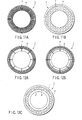
- FIGS. 11A, 11B to 13A, and 13B show mask design for ion implantation, they include radial elements and concentric elements. In the p-type region formed by ion implantation, the radial elements and the concentric elements are integrated (coupled).
- the simple repetitive patterns depicted in FIGS. 11A and 11B being easy to design and manufacture, they are appropriate for the use as long as to obtain the equipotential surfaces.
- the concentric circle (ring) of p-type layers being coupled by radial p-type layers, the dose of the p-type layers is not so large that the patterns have advantages such that the electric potential of each ring becomes lower gradually, namely the electric fields are easily reduced in proportion to getting outside thereof.
- the patterns have advantages such that the electric fields hardly converge to a specific pattern.
- FIGS. 12A to 12C the rings of the inside become wide in the diameter directions, these structures are effective for the use that the equipotential surfaces with high electric potentials at just outside the active regions are bent preferably inside the elements.
- FIGS. 13A and 13B the outer most periphery rings become wide in the diameter directions, and such structures are effective for the user to intend to avoid the concentrations of the electric fields at high-voltage center parts, and conversely, intend to bend the equipotential surfaces at the termination region which has become to a lower potential.
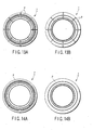
- FIGS. 14A, 14B, and 15A to 15C shapes by which each element is not electrically connected to one another, when they are the p-type layers having effects to bend the equipotential surfaces spreading two-dimensionally from the RESURF layers 8 and the guard rings 9 that are the planar type edge termination parts, the shapes have the similar effects.
- FIGS. 14A and 14B show the examples making the rings at the outsides away from the active regions wide
- FIGS. 15 to 15C show the examples making the rings at the insides wide, and the examples have effects corresponding to each of FIGS. 13, 13B, and 12A to 12C, respectively.
- FIG. 2 depicts the shape like a stripe with respect to the p-type region 5 in the active region.
- the invention is not limited to the shape as long as the openings providing the current path in the p-type region 5, and a variety of variations shown in FIGS. 16A to 16C are possible approaches.
- FIG. 16A illustrating the p-type region 5 having a dotted shape, dots may be formed of n-type and the peripheries thereof may be formed of p-type.
- FIG. 16B showing the p-type region 5 shaped in grid, in a similar way to FIG. 16A, the p-type region and the openings may be reversed.
- FIG. 16C shows the p-type region 5 with a ring shape.
- the openings in the p-type region 5 include openings completely surrounded by the p-type region 5 and the openings the part of which is surrounded by the p-type region 5.
- the p-type region 7 is formed like a ring shape in the outside of the p-type region 5 and is continuously formed from the active region edge to the device edge as shown in FIG. 1, contacting of any one point of the p-type region 7 with the equipotential surface brings the whole of the p-type region 7 into an equipotential surface, so that the electric field concentration hardly occurs.
- the occurrence points of side etching in processing is limited to both side faces of the ring, so that the electric field concentration based on the etching shape is suppressed at minimum.
- the p-type region 5 is formed in a dot pattern, the plural p-type regions can be separately disposed. Thus, the high breakdown voltage is attained by a smaller area.
- the n-type region of the active region is formed in a dot pattern, the electric potential of the p-type regions 5 of a net-shape is made equal at any position therein, and the advantage of the buried p-type region is easily given.
- the ring shape has an advantage to easily ensure the matching property with the edge termination structure. Furthermore, even when no p-type region 5 exists at all, the breakdown voltage may be maintained by the effect of the p-type layer 7.
- the diode since the diode includes the p-type buried region 7 buried in the edge termination region in a sheet shape or a mesh shape substantially in parallel with the surface of the n-type SiC layer 2, when the reverse voltage is applied to the anode electrode 3, and the equipotential surfaces formed at the upper part of the SiC layer 2 being bent toward the direction along the surface of the p-type buried region 7 and also bent so as to converge with one another, the diode becomes possible to have the stable high breakdown voltage characteristic.
- the structure of the first embodiment is such a structure in which only one layer of the p-type regions 5 and 7 is disposed in the n-type SiC layer 2. However, a plurality of stages of p-type buried regions may be disposed in the n-type SiC layer 2.
- FIG. 17 is a cross-sectional view of a semiconductor device according to a second embodiment, and in a similar manner to the first embodiment, the same components as those of the first embodiment are designated by identical numbers to eliminate duplicated descriptions.
- the semiconductor in the second embodiment is also the Schottky barrier diode, and plurality (number n) of the p-type buried layers 5 and 7 are disposed in the n-type SiC layer 2 that is the drift layer. Also in such a device structure, optimizing the impurity concentration and the thickness of the drift layer 2, and optimizing the impurity concentration of the p-type buried regions enable each of the drift layers divided by the plurality (number n) of the p-type buried layers 5 and 7 to share the breakdown voltage, and offers a device with a high breakdown voltage and a low leakage current.
- FIG. 18 is a cross-sectional view of a semiconductor device of the third embodiment, and depicts an embodiment in which the present invention is applied to a pn diode.
- the reference numbers 13, 11 1 and 11 2 indicate a p-type anode region, an Ni anode electrode, and a pad electrode (field plate) of Ti/Al, respectively.
- the same components as those of the first embodiment are designated by identical numbers and duplicated descriptions are omitted.
- the p-type region 13 on the semiconductor surface ohmic-contacting with the anode electrode 11 1 the dose in the p-type region 13 has to be larger than that of the RESURF layer 8. It is preferable for the impurity concentrations of the RESURF layer 8 and the guard rings 9 to be optimally designed so as to match with the impurity concentration of the p-type region 13.
- the pn diode with a stable breakdown voltage characteristic may be offered by disposing the p-type buried layer 7 that is an equipotential surface convergence structure.
- FIG. 19 is a cross-sectional view of a semiconductor device according to the fourth embodiment, and shows an embodiment in which the invention is applied to a vertical MOSFET.
- FIG. 19 shows a p-type region 14, an n-type source region 15, a (gate) insulating region 16, a gate electrode 17, and a source electrode (first electrode) 18.
- the same components as those of the first embodiment are designated by identical numbers and duplicated descriptions are skipped, and the reference number 4 indicates the drain electrode (second electrode).
- Disposing the n-type SiC semiconductor layer 2 onto the p-type SiC semiconductor substrate 1 enables composing an IGBT.
- disposing the p-type buried region 7 that is an equipotential surface convergence structure in an edge termination region allows achieving a vertical MOSFET having a stable breakdown voltage characteristic.
- the semiconductor material is not limited to SiC; it goes without saying that adaptation to Si, GaN, diamond, etc., are effective similarly.
- the conductivity type of the substrate and semiconductor layer may be reversible.
Landscapes
- Electrodes Of Semiconductors (AREA)
Abstract
Description
- The present invention relates to a high-voltage semiconductor device which develops a stable breakdown voltage characteristic.
- Conventionally, a high-voltage diode and a MOSFET have been used as a semiconductor device for electric power control. Such a kind of semiconductor device has been required to improve conflicting characteristics, such as, an improvement in breakdown voltage and a reduction in on-state resistance, and a variety of proposals on this requirement have been offered.
- For example,
JP-A H9-191109 - After that, as raising the reverse bias voltage, the depletion layer reaches the p-type buried layer, the largest point of the electric field at the Schottky interface is fixed not to be raised, and the depletion layer newly spreads onto an ohmic electrode side from the buried layer. Here, the voltage held by the epitaxial layer between the Schottky interface and the buried layer is set to a value lower than the maximum blocking (breakdown) voltage. Thereby, the electric field at the Schottky interface is fixed to a low value, and the leakage current from the Schottky interface may be decreased.
- The technique disclosed in the aforementioned patent document disposes a plurality of stages of p-type buried layers as depicted in FIG. 13 of said patent document, shares a breakdown voltage by means of n-type base layers divided by the plurality of stages of p-type buried layers, and develops a Schottky barrier diode which achieves a small voltage drop when conducting at a high voltage.
- However, the forgoing conventional improvement is specified only for an active region under an anode electrode, and it does not take so much account to an n-type base layer under an edge termination structure. In other words, specifically, a planer-type high-voltage device, though it has high-voltage performance based on the p-type layer buried in the active region, it poses the problem that the breakdown voltage is determined by an electric field concentration at an edge termination region. If the edge termination structure is microscopic like guard rings, and when widths and intervals of the patterns vary due to a mask misalignment, the problem of lowering in breakdown voltage occurs.
- Although such a problem poses, the planer device has many advantages for mass production on those points which are more stable in process, and are higher in yield ration and in throughput than a mesa-type device. Therefore, it has been desired to attain a high-breakdown-voltage device having a planar structure stable in breakdown voltage.
- According to one aspect of the invention, there is provided a semiconductor device, which includes:
- a semiconductor substrate of a first conductivity type having a top surface and a bottom surface;
- a semiconductor layer of a first conductivity type formed on the top surface of the semiconductor substrate, and having an active region and an edge termination region surrounding the active region;
- a first semiconductor region of a second conductivity type formed in the edge termination region adjacent to an edge of the active region;
- a second semiconductor region of a second conductivity type buried in the edge termination region in a sheet shape or a mesh shape substantially in parallel with a surface of the semiconductor layer.
- a first electrode formed on the active region of the semiconductor layer and a part of the first semiconductor region; and
- a second electrode formed on the bottom surface of the semiconductor substrate.
- The invention can be more fully understood from the following detailed description when taken in conjunction with the accompanying drawings, in which:
- FIG. 1 is an exemplary longitudinal sectional view of one element of a Schottky barrier diode according to the first embodiment;
- FIG. 2 is an exemplary transverse sectional view along a II-II line of FIG. 1;
- FIG. 3 is an exemplary schematic view depicting equipotential surfaces when a reverse bias is applied to the diode of FIG. 1;
- FIG. 4 is an exemplary schematic view depicting equipotential surfaces when a reverse bias is applied to a diode in a comparison example;
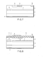
- FIGS. 5 to 8 are exemplary longitudinal sectional views for explaining manufacturing process of the diode in the first embodiments step by step;
- FIG. 9 is an exemplary characteristic view depicting a relation between an inside start point position and a breakdown voltage of a buried p-
type region 7; - FIG. 10 is an exemplary characteristic view depicting a relation between the breakdown voltage and an outside end point position of the buried p-
type region 7; - FIGS. 11A and 11B are exemplary pattern examples of the buried p-
type regions 7; - FIGS. 12A to 12C are exemplary other pattern examples of the buried p-
type regions 7; - FIGS. 13A, 13B, 14A, 14B, and 15A to 15C are exemplary further other pattern examples of the buried p-
type regions 7; - FIGS. 16A to 16C are exemplary pattern examples of buried p-
type regions 5, - FIG. 17 is an exemplary longitudinal sectional view of a Schottky barrier diode according to the second embodiment;
- FIG. 18 is an exemplary longitudinal sectional view of a pn diode according to the third embodiment; and
- FIG. 19 is an exemplary longitudinal sectional view of a vertical MOSFET according to the fourth embodiment.
- A semiconductor device of the present invention described in the following embodiments is provided with a second semiconductor region of a second conductivity type buried in a sheet shape or a mesh shape in an edge termination region of a semiconductor layer of a first conductivity type substantially in parallel with the surface of the semiconductor layer. When a reverse voltage is applied between a first electrode and a second electrode, equipotential surfaces formed on upper parts of the semiconductor layer being bent toward a direction along the surface of the second semiconductor region so as to be converged with each other. As an electric field distribution is thus formed, the semiconductor device is hard to be broken at the edge termination region and has a stable breakdown voltage characteristic.
- Hereinafter, the embodiments of the invention will be described with reference to the drawings.
- FIG. 1 is a longitudinal sectional view of one element of a semiconductor device (vertical Schottky barrier diode) according to the first embodiment. FIG. 2 illustrates a schematic transverse sectional view along a II-II line of FIG. 1, and constituent components of one element of the embodiment are formed in a concentric circle shape in a plane except a component of
reference number 5. In FIG. 2, the constituent components may be modified and formed such that components ofreference numbers - In further detail, n-type
SiC semiconductor layer 2 is formed on a highly doped n+-typeSiC semiconductor substrate 1. ARESURF layer 8 containing p-type impurities is formed in an annular shape so as to surround an active region A at a surface central part of theSiC semiconductor layer 2. If further high-breakdown voltage is required, it is preferable to form an edge termination layer (not shown) containing p+ type impurities inside theRESURF layer 8 so as to lie under an anode electrode edge. - P-
type guard rings 9 are formed so as to surround theRESURF layer 8 of p-type in order to further enhance the breakdown voltage. In this case, the guard rings 9 of p-type may further enhance effect by disposing a plurality thereof. The sameness of the impurity concentration in theRESURF layer 8 and theguard rings 9 makes easy in a manufacturing process, however it may be different from one another. The semiconductor device may include either theRESURF layer 8 or theguard rings 9. - The surface of the active region surrounded by the
RESURF layer 8 is provided with afirst electrode 3 so as to be contacted with the surface. Thefirst electrode 3 forms a Schottky junction with theSiC semiconductor layer 2, and uses, for example, Ti as a material. A pad electrode (or a field plate) 11 electrically connected to thefirst electrode 3 is formed thereon by, for example, Al. The pad electrode (field plate) 11 is formed also above the edge termination structure of theSiC semiconductor layer 2 with theRESURF layer 8 or theguard rings 9 formed thereon through a field-plate insulating film 12. The electric field being apt to concentrate to the edge part of thefield plate 11 when the reverse electric field is applied thereto, it is preferable to be structured such that the edge part is disposed on the upper part of theRESIRF layer 8 or theguard rings 9. Asecond electrode 4 is formed on the bottom face of theSiC semiconductor substrate 1 by, for instance, Ni. - In the semiconductor device, p-
type semiconductor regions SiC semiconductor layer 2 in order to be formed in a low-loss structure, namely in a high-breakdown voltage and low on-state resistance structure. In further detail, a p-type region 5 having a plurality of openings is formed in order to have a high breakdown voltage structure and to secure a current path in the active region at the central part of the semiconductor device. As the buried termination structure in the edge termination region, the p-type region 7 is disposed in an electrically continued manner up to a device periphery on the outside of the active region. The periphery of the surface of the n-type semiconductor layer 2 is provided with anedge termination region 10 of a highly doped n+-type semiconductor. - Operations of the semiconductor device will be described hereinafter. When a reverse voltage is applied to the
first electrode 3 that is an anode electrode, the depletion layer spreads in the device in the direction toward a second electrode through a Schottky interface, and also it spreads in the direction toward theRESURF layer 8 and the guard rings 9, namely in a lateral direction of the device. The depletion layer extended in the lateral direction spreads in the lateral direction while being pinned by theRESURF layer 8 and the guard rings 9. - After this, the depletion layer reaches the p-type buried
regions type region 5 only two-dimensionally; however the depletion layer spreads toward the p-type region 7 three-dimensionally. To achieve a high-breakdown voltage device, the electric field on the semiconductor surface should be kept lower than the maximum electric field intensity, and also the depletion layer should not be spread up to the second electrode. - In the case in which the p-type buried
region 7 like one in this embodiment exists, as depicted in FIG. 3, the equipotential surface spreading in an oblique direction may be bent in a direction further parallel to the surface of the buriedregion 7, that is, may be bent so as to be converged along with the surface of the buriedregion 7. Conversely, in the case in which the buriedregion 7 like this does not exist, or on such a device in FIG. 4 in which the buriedregions 5 at the center are formed to extend to the periphery thereof, all of the equipotential surfaces cannot be converged along the surface of the buriedregions 5 because gaps (openings) are present in the buriedregions 5 at the periphery thereof. - Like this, according to the first embodiment, in comparison to the device including no p-type buried
region 7, the depletion layer does not reach the second electrode and a device with a further high breakdown voltage may be achieved. It is preferable for the aforementioned device to be designed such that the maximum electric field intensity becomes larger than the electric field with respect to the p-type buriedregions - Next to this, a manufacturing method of the foregoing semiconductor device will be described by referring to FIGS. 5 to 8. The longitudinal sectional view of the semiconductor of the embodiment is a symmetrical shape capable of being folded at a center line of each of FIGS. 5 to 8, so that only a right half thereof will be illustrated hereinafter to simplify FIGS. 5 to 8.
- At first, the method, as shown in FIG. 5, forms a film of the n-
type SiC layer 2 on the n+SiC semiconductor substrate 1 by epitaxial growth. Here, the impurity concentration of the n-type SiC substrate 1 is, for example, 3×10¹⁵ to 3×10¹⁶/cm3 inclusive, and the present embodiment takes the case of the concentration of 1×10¹⁶/cm3 as an example. The thickness of theSiC semiconductor layer 2 ranges from several µm to several dozen µm, and this embodiment sets it to 10 µm. - On the n-
type SiC layer 2, as illustrated in FIG. 6, the method forms the buriedlayer 5 under the active region and the buriedlayer 7 for burying the edge termination region simultaneously. Firstly applying and film-forming a mask material onto the surface of theSiC semiconductor layer 1 to perform patterning forms desired mask patterns (not shown) of the p-type buriedregions regions - Here, as for p-type ion species, aluminum (Al), boron (B), etc., are usually used; however in the embodiment, Al suitable for a fine pattern is used. As for ion accelerating energy, energy of several keV to several hundred keV is usually used, and in the embodiment, the method uses the ion accelerating energy of 100-360 keV. An ion dose is set to its optimum value by a designed breakdown voltage and an epitaxial concentration, and the method performs Al multi-level ion implantation through the energy of, for example, from 100 to 360 keV inclusive with a dose ranging from 1×10¹³ to 1×10¹⁴/cm2 inclusive. In such a case, the method may form a p-type well having a concentration ranging from 1×10¹⁷ to 5×10¹⁸/cm3 inclusive.
- The case, in which the concentrations of the p-type buried
regions region 5, and performing the ion implantation into the p-type buriedregion 5, the method peels off the mask, forms the p-type buriedregion 7 again, and performs the ion implantation into the p-type buriedregion 7. Or, after performing the ion implantation into the p-type buriedregion 7 in first, the method may implant ions into the p-type buriedregion 5. Therefore, the sameness of the concentrations of the p-type buriedregions - Subsequently, as shown in FIG. 7, the method grows again the upper part of the n-
type SiC layer 2 onto the upper surface of the ion implantation surface by the epitaxial growth layer. The concentration and thickness of the upper part of the n-type SiC layer 2 is set to substantially the same as those of the aforementioned lower part of theSiC layer 2. After this, the method forms an n+-typechannel stopper layer 10, the p-type RESURF layer 8 and the guard rings 9 on the surface of the n-type SiC layer 2. - The method forms these layers by forming a mask pattern to selectively implanting ions, and it uses nitrogen (N) and phosphorus (P) for n-type ion species. Those doping concentrations being determined by the desired impurity concentration of the n-
type SiC layer 2, it is enough for thechannel stopper layer 10 to become an n+ layer perfectly, and the doping concentration ranges, for example, from 1×10¹⁴ to 1x10¹⁶/cm2 inclusive, and here, it is set to 2×10¹⁵/cm2. - The optimum values of the p-
type RESURF layer 8 and the guard rings 9 are set by the designed breakdown voltage and the epitaxial concentration, the dose is set to 1×10¹³ to 1×10¹⁴/cm2 inclusive by Al multi-level ion plantation with, for example, 10-360 keV energy. In this case, the method may form p-type wells having a concentration within a range from 1×10¹⁷ to 5×10¹⁸/cm3 inclusive. To activate these wells, the method executes activated anneal at a high temperature within a range from 1,500 to 1,700°C inclusive after ion implantation. - The impurity concentrations of the p-
type RESURF layer 8 and theguard ring 9 being set to the same as that of the p-type buriedlayer 7, they are not always necessary to be the same and they may be different form one another. However, the sameness of the impurity concentrations of the p-type RESURF layer 8 and the guard rings 9 makes the method easy in process. - After this, the method forms a
silicon dioxide film 12 through thermal oxidation and a chemical vapor deposition (CVD) oxide film. After this, the method forms the second electrode on the bottom surface. The appropriate electrode material to this forming is a material to be easily ohmic-contacted, here, for example, Ni is used. Furthermore, to make sure the ohmic contact, the method preferably performs a thermal treatment at a high temperature of 900°C or higher. To lower the contact resistance of the bottom electrode, the method preferably forms a film of a Ti/Ni/Au laminated structure, etc., onto the Ni surface. - The method then selectively performs etching to the
silicon oxide film 12 of the surface to open a contact hole and to form aSchottky metal film 3. As for the Schottky metal material, a metallic material to make a Schottky-contact to a SiC face may be preferable, and here, for example, Ti is used. Thepad electrode 11 made of Al is formed so as to overlap on theSchottky metal film 3 and also on thesilicon oxide film 12. Finally, the method applies passivation (not shown) by polyimide, or the like, as part of a high breakdown voltage structure to complete the element. - In the given description, the case, in which the method performs the multi-level implantation by the low acceleration energy and the re-growing of the drift layer, having been described. If the drift layer has a thickness of 10 µm or less, after growing the drift layer up to the final thickness in first, the method may form the p-type buried region at only a prescribed depth thereof by performing multi-level implantation with high acceleration energy.
- The first embodiment given above having described about the shape in which the p-type buried
region 7 is arranged from almost edge part of the active region (under the inside edge part of the RESURF layer 8) up to the almost edge part of the device, the invention is not limited to this. FIG. 9 shows the result from a simulation of a breakdown voltage by varying a position of a start point (distance outward from active region edge) while fixing the edge of the p-type region 7 in theSiC semiconductor layer 2 to the device edge part. Here, the inside edge of theRESURF layer 8 is adjacent to the active region, and the width of theRESURF layer 8 is set to 50 µm. In addition, theRESURF layer 8 may be larger than 50 µm in width as long as there is some distance between theRESURF layer 8 and the device edge. From FIG. 9, it is revealed that the inner edge of the p-type buriedlayer 7 located under theRESURF layer 8 makes the breakdown voltage higher. That is, the inner edge of the p-type buriedlayer 7 is desirably set inside the outer edge of theRESURF layer 8. Of course, the result tells that the inner edge of the p-type buriedlayer 7 may be inside the active region edge. FIG. 10 illustrates the result of a simulation of a breakdown voltage by varying the edge termination end point while fixing the start point to the active region edge. It is clear that the highest breakdown voltage is attainable in the case where the outside edge of the p-type region 7 is 20 µm or more outside from the outer edge of theRESURF layer 8. - In the first embodiment, the shape, in which the buried p-type region extends from the active region edge to the device edge in a sheet shape, having been described, the invention is not limited to this embodiment. For instance, as shown in FIGS. 11A, 11B to 13A, and 13B, even when the openings are present in the p-type region, if the p-type regions are electrically connected to each other at the edge termination part, an effect to converge the equipotential surfaces on the face of the p-type region is obtained. FIGS. 11A, 11B to 13A, and 13B show mask design for ion implantation, they include radial elements and concentric elements. In the p-type region formed by ion implantation, the radial elements and the concentric elements are integrated (coupled).
- The simple repetitive patterns depicted in FIGS. 11A and 11B being easy to design and manufacture, they are appropriate for the use as long as to obtain the equipotential surfaces. In the case of FIG. 11A, the concentric circle (ring) of p-type layers being coupled by radial p-type layers, the dose of the p-type layers is not so large that the patterns have advantages such that the electric potential of each ring becomes lower gradually, namely the electric fields are easily reduced in proportion to getting outside thereof. Conversely, in the case of dotted shape of FIG. 11B, the patterns have advantages such that the electric fields hardly converge to a specific pattern.
- In FIGS. 12A to 12C, the rings of the inside become wide in the diameter directions, these structures are effective for the use that the equipotential surfaces with high electric potentials at just outside the active regions are bent preferably inside the elements. In FIGS. 13A and 13B, the outer most periphery rings become wide in the diameter directions, and such structures are effective for the user to intend to avoid the concentrations of the electric fields at high-voltage center parts, and conversely, intend to bend the equipotential surfaces at the termination region which has become to a lower potential.
- Even if the buried p-
type regions 7 have, as shown in FIGS. 14A, 14B, and 15A to 15C, shapes by which each element is not electrically connected to one another, when they are the p-type layers having effects to bend the equipotential surfaces spreading two-dimensionally from the RESURF layers 8 and the guard rings 9 that are the planar type edge termination parts, the shapes have the similar effects. FIGS. 14A and 14B show the examples making the rings at the outsides away from the active regions wide, and FIGS. 15 to 15C show the examples making the rings at the insides wide, and the examples have effects corresponding to each of FIGS. 13, 13B, and 12A to 12C, respectively. - FIG. 2 depicts the shape like a stripe with respect to the p-
type region 5 in the active region. However, the invention is not limited to the shape as long as the openings providing the current path in the p-type region 5, and a variety of variations shown in FIGS. 16A to 16C are possible approaches. FIG. 16A illustrating the p-type region 5 having a dotted shape, dots may be formed of n-type and the peripheries thereof may be formed of p-type. FIG. 16B showing the p-type region 5 shaped in grid, in a similar way to FIG. 16A, the p-type region and the openings may be reversed. FIG. 16C shows the p-type region 5 with a ring shape. Like this, the openings in the p-type region 5 include openings completely surrounded by the p-type region 5 and the openings the part of which is surrounded by the p-type region 5. - When the p-
type region 7 is formed like a ring shape in the outside of the p-type region 5 and is continuously formed from the active region edge to the device edge as shown in FIG. 1, contacting of any one point of the p-type region 7 with the equipotential surface brings the whole of the p-type region 7 into an equipotential surface, so that the electric field concentration hardly occurs. The occurrence points of side etching in processing is limited to both side faces of the ring, so that the electric field concentration based on the etching shape is suppressed at minimum. When the p-type region 5 is formed in a dot pattern, the plural p-type regions can be separately disposed. Thus, the high breakdown voltage is attained by a smaller area. Further, it has an advantage to allow reducing the on-state resistance. Conversely, when the n-type region of the active region is formed in a dot pattern, the electric potential of the p-type regions 5 of a net-shape is made equal at any position therein, and the advantage of the buried p-type region is easily given. The ring shape has an advantage to easily ensure the matching property with the edge termination structure. Furthermore, even when no p-type region 5 exists at all, the breakdown voltage may be maintained by the effect of the p-type layer 7. - As mentioned above, according to the first embodiment, since the diode includes the p-type buried
region 7 buried in the edge termination region in a sheet shape or a mesh shape substantially in parallel with the surface of the n-type SiC layer 2, when the reverse voltage is applied to theanode electrode 3, and the equipotential surfaces formed at the upper part of theSiC layer 2 being bent toward the direction along the surface of the p-type buriedregion 7 and also bent so as to converge with one another, the diode becomes possible to have the stable high breakdown voltage characteristic. - The structure of the first embodiment is such a structure in which only one layer of the p-
type regions type SiC layer 2. However, a plurality of stages of p-type buried regions may be disposed in the n-type SiC layer 2. FIG. 17 is a cross-sectional view of a semiconductor device according to a second embodiment, and in a similar manner to the first embodiment, the same components as those of the first embodiment are designated by identical numbers to eliminate duplicated descriptions. - The semiconductor in the second embodiment is also the Schottky barrier diode, and plurality (number n) of the p-type buried
layers type SiC layer 2 that is the drift layer. Also in such a device structure, optimizing the impurity concentration and the thickness of thedrift layer 2, and optimizing the impurity concentration of the p-type buried regions enable each of the drift layers divided by the plurality (number n) of the p-type buriedlayers - FIG. 18 is a cross-sectional view of a semiconductor device of the third embodiment, and depicts an embodiment in which the present invention is applied to a pn diode. The
reference numbers - In the third embodiment, the p-
type region 13 on the semiconductor surface ohmic-contacting with theanode electrode 111, the dose in the p-type region 13 has to be larger than that of theRESURF layer 8. It is preferable for the impurity concentrations of theRESURF layer 8 and theguard rings 9 to be optimally designed so as to match with the impurity concentration of the p-type region 13. - Also in the third embodiment, the pn diode with a stable breakdown voltage characteristic may be offered by disposing the p-type buried
layer 7 that is an equipotential surface convergence structure. - FIG. 19 is a cross-sectional view of a semiconductor device according to the fourth embodiment, and shows an embodiment in which the invention is applied to a vertical MOSFET. FIG. 19 shows a p-
type region 14, an n-type source region 15, a (gate) insulatingregion 16, agate electrode 17, and a source electrode (first electrode) 18. Other than these, the same components as those of the first embodiment are designated by identical numbers and duplicated descriptions are skipped, and thereference number 4 indicates the drain electrode (second electrode). Disposing the n-typeSiC semiconductor layer 2 onto the p-typeSiC semiconductor substrate 1 enables composing an IGBT. - In the fourth embodiment, disposing the p-type buried
region 7 that is an equipotential surface convergence structure in an edge termination region allows achieving a vertical MOSFET having a stable breakdown voltage characteristic. - The invention having been described through the embodiments, the semiconductor material is not limited to SiC; it goes without saying that adaptation to Si, GaN, diamond, etc., are effective similarly. The conductivity type of the substrate and semiconductor layer may be reversible.
Claims (20)
- A semiconductor device, characterized by comprising;a semiconductor substrate (1) of a first conductivity type having a top surface and a bottom surface;a semiconductor layer (2) of a first conductivity type formed on the top surface of the semiconductor substrate (1), and having an active region and an edge termination region surrounding the active region;a first semiconductor region (8, 14) of a second conductivity type formed in the edge termination region adjacent to an edge of the active region;a second semiconductor region (7) of a second conductivity type buried in the edge termination region in a sheet shape or a mesh shape substantially in parallel with a surface of the semiconductor layer (2);a first electrode (3 18) formed on the active region of the semiconductor layer (2) and a part of the first semiconductor region (8, 14); anda second electrode (4) formed on the bottom surface of the semiconductor substrate (1).
- The device according to claim 1, characterized in that an impurity concentration of the first semiconductor region (8) is substantially equal to that of the second semiconductor region (7), and the first semiconductor region (8) functions as a RESURF region.
- The device according to claim 1, characterized by further comprising:a third semiconductor region (5) of a second conductivity type at a substantially same depth as that of the second semiconductor region (7) in the active region of the semiconductor layer (2).
- The device according to claim 3, characterized in that the third semiconductor region (5) includes a plurality of openings.
- The device according to claim 1, characterized in that equipotential surfaces formed in an upper portion of the semiconductor layer (2) are bent along a surface of the second semiconductor region (7) to be converged with one another when a reverse voltage is applied between the first electrode (3) and the second electrode (4).
- The device according to claim 1, characterized by further comprising:a guard ring (9) of a second conductivity type formed on the edge termination region of the semiconductor layer (2) so as to surround the first semiconductor region (8, 14) with a space.
- The device according to claim 1, characterized by further comprising:a fourth semiconductor region (10) of a first conductivity type formed on a peripheral edge surface of the semiconductor layer (2) so as to surround the first semiconductor region (8, 14) with a space and has an impurity concentration higher than that of the semiconductor layer (2).
- The device according to claim 1, characterized in that the second semiconductor region (7) includes a plurality of openings to form a mesh region.
- The device according to claim 1, characterized in that the semiconductor substrate (1) and the semiconductor layer (2) are formed of SiC.
- The device according to claim 9, characterized in that an inner edge of the second semiconductor region (7) is set inside an outer edge of the first semiconductor region (8, 14) and an outer edge of the second semiconductor region (7) is set 20 µm or more outside the outer edge of the first semiconductor region (8, 14).
- The device according to claim 9, characterized in that an impurity concentration of the second semiconductor region (7) falls in a range between 1×10¹⁷/cm3 inclusive and 5×10¹⁸/cm3 inclusive.
- The device according to claim 9, characterized in that an impurity concentration of the third semiconductor region (5) falls in a range between 1×10¹⁷/cm3 inclusive and 5×10¹⁸/cm3 inclusive.
- A semiconductor device, characterized by comprising:a semiconductor substrate (1) of a first conductivity type having a top surface and a bottom surface;a semiconductor layer (2) of a first conductivity type formed on the top surface of the semiconductor substrate (1), and having an active region and an edge termination region surrounding the active region;a RESURF region (8) of a second conductivity type formed in the edge termination region adjacent to an edge of the active region with a space;a guard ring (9) formed in the semiconductor layer (2) so as to surround the RESURF layer (8) with a space; anda first buried semiconductor region (7) of a second conductivity type buried in the edge termination region in a sheet shape or a mesh shape substantially in parallel with a surface of the semiconductor layer (2);a first electrode (3) formed on the active region of the semiconductor layer (2) and a part of the RESURF region (8);an insulating layer (12) covering the semiconductor layer (2) so as to surround the first electrode (3); anda second electrode (4) formed on the bottom surface of the semiconductor substrate (1);
- The device according to claim 13, characterized by further comprising:a second buried semiconductor region (5) of a second conductivity type buried at the substantially same depth as that of the first buried semiconductor region (7) in the active region inside the RESURF region (8).
- The device according to claim 13, characterized in that equipotential surfaces formed in an upper portion of the semiconductor layer (2) are bent along a surface of the first buried semiconductor region (7) to be converged with one another, when a reverse voltage is applied between the first electrode (3) and the second electrode (4).
- The device according to claim 13,
characterized by further comprising:a channel stopper region (10) of a first conductivity type formed at a periphery end part of the semiconductor layer (2) so as to surround the guard ring (9) with a space and has an impurity concentration higher than that of the semiconductor layer (2). - The device according to claim 13, characterized in that the first buried semiconductor region (7) includes a plurality of openings to form a mesh region.
- The device according to claim 13, characterized in that the semiconductor substrate (1) and the semiconductor layer (2) are formed of SiC.
- The device according to claim 18, characterized in that an impurity concentration of the first buried region (7) falls in a range between 1×10¹⁷/cm3 inclusive and 5×10¹⁸/cm3 inclusive.
- The device according to claim 18, characterized in that an impurity concentration of the second buried region (5) falls in a range between 1x10¹⁷/cm3 inclusive and 5×10¹⁸/cm3 inclusive.
Applications Claiming Priority (1)
| Application Number | Priority Date | Filing Date | Title |
|---|---|---|---|
| JP2006182703A JP4189415B2 (en) | 2006-06-30 | 2006-06-30 | Semiconductor device |
Publications (2)
| Publication Number | Publication Date |
|---|---|
| EP1873839A2 true EP1873839A2 (en) | 2008-01-02 |
| EP1873839A3 EP1873839A3 (en) | 2009-03-04 |
Family
ID=38512391
Family Applications (1)
| Application Number | Title | Priority Date | Filing Date |
|---|---|---|---|
| EP07012590A Withdrawn EP1873839A3 (en) | 2006-06-30 | 2007-06-27 | Semiconductor device |
Country Status (4)
| Country | Link |
|---|---|
| US (1) | US7777292B2 (en) |
| EP (1) | EP1873839A3 (en) |
| JP (1) | JP4189415B2 (en) |
| CN (1) | CN101097947A (en) |
Cited By (1)
| Publication number | Priority date | Publication date | Assignee | Title |
|---|---|---|---|---|
| EP3010045A1 (en) * | 2014-10-14 | 2016-04-20 | Hitachi, Ltd. | Semiconductor device and a method of manufacturing same |
Families Citing this family (70)
| Publication number | Priority date | Publication date | Assignee | Title |
|---|---|---|---|---|
| TWI278090B (en) | 2004-10-21 | 2007-04-01 | Int Rectifier Corp | Solderable top metal for SiC device |
| US7812441B2 (en) | 2004-10-21 | 2010-10-12 | Siliconix Technology C.V. | Schottky diode with improved surge capability |
| US9419092B2 (en) | 2005-03-04 | 2016-08-16 | Vishay-Siliconix | Termination for SiC trench devices |
| US8368165B2 (en) | 2005-10-20 | 2013-02-05 | Siliconix Technology C. V. | Silicon carbide Schottky diode |
| JP2009545885A (en) * | 2006-07-31 | 2009-12-24 | ヴィシェイ−シリコニックス | Molybdenum barrier metal for SiC Schottky diode and manufacturing method |
| US7955929B2 (en) * | 2007-01-10 | 2011-06-07 | Freescale Semiconductor, Inc. | Method of forming a semiconductor device having an active area and a termination area |
| US7781859B2 (en) * | 2008-03-24 | 2010-08-24 | Taiwan Semiconductor Manufacturing Company, Ltd. | Schottky diode structures having deep wells for improving breakdown voltages |
| JP4743447B2 (en) * | 2008-05-23 | 2011-08-10 | 三菱電機株式会社 | Semiconductor device |
| JP5366297B2 (en) * | 2009-02-10 | 2013-12-11 | 富士電機株式会社 | Semiconductor device |
| JP5375270B2 (en) * | 2009-03-31 | 2013-12-25 | トヨタ自動車株式会社 | Semiconductor device |
| JP5391447B2 (en) * | 2009-04-06 | 2014-01-15 | 三菱電機株式会社 | Semiconductor device and manufacturing method thereof |
| CN102217070B (en) * | 2009-09-03 | 2013-09-25 | 松下电器产业株式会社 | Semiconductor device and method for producing same |
| DE102009047808B4 (en) * | 2009-09-30 | 2018-01-25 | Infineon Technologies Austria Ag | Bipolar semiconductor device and method for producing a semiconductor diode |
| JP5544918B2 (en) * | 2010-02-16 | 2014-07-09 | 住友電気工業株式会社 | Silicon carbide insulated gate type semiconductor device and manufacturing method thereof |
| US8476698B2 (en) * | 2010-02-19 | 2013-07-02 | Alpha And Omega Semiconductor Incorporated | Corner layout for superjunction device |
| JP5537996B2 (en) * | 2010-03-03 | 2014-07-02 | 株式会社東芝 | Semiconductor device |
| JP5072991B2 (en) * | 2010-03-10 | 2012-11-14 | 株式会社東芝 | Semiconductor device |
| CN102315281B (en) * | 2010-09-07 | 2013-09-18 | 成都芯源系统有限公司 | Schottky diode and manufacturing method thereof |
| JP5474218B2 (en) * | 2010-12-28 | 2014-04-16 | 三菱電機株式会社 | Semiconductor device |
| JP5558393B2 (en) | 2011-03-10 | 2014-07-23 | 株式会社東芝 | Semiconductor device |
| US8466491B2 (en) * | 2011-05-12 | 2013-06-18 | Infineon Technologies Austria Ag | Semiconductor component with improved softness |
| CN103534810B (en) * | 2011-05-18 | 2017-05-17 | 罗姆股份有限公司 | Semiconductor device and method for producing same |
| CN102800670A (en) * | 2011-05-27 | 2012-11-28 | 硕颉科技股份有限公司 | Single chip type metal oxide semiconductor field effect transistor-Schottky diode element |
| US8618582B2 (en) * | 2011-09-11 | 2013-12-31 | Cree, Inc. | Edge termination structure employing recesses for edge termination elements |
| JP2013120822A (en) * | 2011-12-07 | 2013-06-17 | Sumitomo Electric Ind Ltd | Semiconductor device manufacturing method |
| JP5928101B2 (en) * | 2012-03-30 | 2016-06-01 | 富士電機株式会社 | Method for manufacturing SiC semiconductor device |
| CN103681809B (en) * | 2012-09-09 | 2016-08-17 | 苏州英能电子科技有限公司 | There is the lateral bipolar transistor of composite construction |
| CN103681317A (en) * | 2012-09-18 | 2014-03-26 | 桂林斯壮微电子有限责任公司 | Method for manufacturing P-N junction buried barrier Schottky diode |
| CN103681781A (en) * | 2012-09-18 | 2014-03-26 | 桂林斯壮微电子有限责任公司 | Buried PN junction barrier Schottky diode |
| US8766396B2 (en) * | 2012-11-02 | 2014-07-01 | Moxtek, Inc. | Vibration noise shield in a semiconductor sensor |
| DE102013018789B4 (en) * | 2012-11-29 | 2025-03-06 | Infineon Technologies Ag | Controlling light-generated charge carriers |
| JP5958352B2 (en) | 2013-01-15 | 2016-07-27 | 住友電気工業株式会社 | Silicon carbide semiconductor device and manufacturing method thereof |
| JP5983415B2 (en) | 2013-01-15 | 2016-08-31 | 住友電気工業株式会社 | Silicon carbide semiconductor device |
| JP6089733B2 (en) * | 2013-01-30 | 2017-03-08 | 富士電機株式会社 | Semiconductor device |
| JP6075120B2 (en) * | 2013-03-01 | 2017-02-08 | 住友電気工業株式会社 | Silicon carbide semiconductor device |
| JP2014175518A (en) | 2013-03-11 | 2014-09-22 | Sumitomo Electric Ind Ltd | Silicon carbide semiconductor device |
| US9035322B2 (en) | 2013-03-26 | 2015-05-19 | Infineon Technologies Ag | Silicon carbide device and a method for manufacturing a silicon carbide device |
| US9257511B2 (en) | 2013-03-26 | 2016-02-09 | Infineon Technologies Ag | Silicon carbide device and a method for forming a silicon carbide device |
| JP2014232838A (en) * | 2013-05-30 | 2014-12-11 | 住友電気工業株式会社 | Silicon carbide semiconductor device |
| US9768259B2 (en) | 2013-07-26 | 2017-09-19 | Cree, Inc. | Controlled ion implantation into silicon carbide using channeling and devices fabricated using controlled ion implantation into silicon carbide using channeling |
| US9431490B2 (en) | 2013-08-09 | 2016-08-30 | Infineon Technologies Austria Ag | Power semiconductor device and method |
| CN103413822B (en) * | 2013-08-22 | 2016-05-18 | 中国电子科技集团公司第二十四研究所 | Reduce the method for floating empty buried regions semiconductor device creepage |
| JP6139355B2 (en) * | 2013-09-24 | 2017-05-31 | トヨタ自動車株式会社 | Semiconductor device |
| JP6224454B2 (en) * | 2013-12-27 | 2017-11-01 | 株式会社豊田中央研究所 | Vertical semiconductor device |
| KR101518905B1 (en) * | 2013-12-30 | 2015-05-11 | 현대자동차 주식회사 | Shottky barrier diode and method for manufacturing the same |
| JP2015220437A (en) * | 2014-05-21 | 2015-12-07 | 住友電気工業株式会社 | Silicon carbide semiconductor device |
| CN104241338B (en) * | 2014-09-29 | 2017-06-13 | 中国科学院微电子研究所 | A kind of SiC metal oxide semiconductor transistor and its manufacturing method |
| DE102015106707A1 (en) * | 2015-04-30 | 2016-11-03 | Infineon Technologies Austria Ag | Semiconductor devices and methods of forming a semiconductor device |
| JP2016219475A (en) * | 2015-05-15 | 2016-12-22 | トヨタ自動車株式会社 | Method for manufacturing silicon carbide semiconductor device |
| JP2017011060A (en) * | 2015-06-19 | 2017-01-12 | 住友電気工業株式会社 | Schottky barrier diode |
| US9735237B2 (en) * | 2015-06-26 | 2017-08-15 | General Electric Company | Active area designs for silicon carbide super-junction power devices |
| JP6550995B2 (en) * | 2015-07-16 | 2019-07-31 | 富士電機株式会社 | Semiconductor device |
| JP6479615B2 (en) | 2015-09-14 | 2019-03-06 | 株式会社東芝 | Manufacturing method of semiconductor device |
| JP6767705B2 (en) * | 2016-04-28 | 2020-10-14 | パナソニックIpマネジメント株式会社 | Semiconductor element |
| JP6719090B2 (en) * | 2016-12-19 | 2020-07-08 | パナソニックIpマネジメント株式会社 | Semiconductor element |
| WO2019008884A1 (en) * | 2017-07-04 | 2019-01-10 | 住友電気工業株式会社 | Silicon carbide semiconductor device |
| JP7327905B2 (en) | 2017-07-07 | 2023-08-16 | 株式会社デンソー | Semiconductor device and its manufacturing method |
| CN107482052B (en) * | 2017-07-21 | 2021-01-29 | 泰科天润半导体科技(北京)有限公司 | Silicon carbide power device with buried N-type channel and manufacturing method thereof |
| JP2019054170A (en) * | 2017-09-15 | 2019-04-04 | 株式会社東芝 | Semiconductor device |
| TWI635611B (en) * | 2017-09-25 | 2018-09-11 | Nuvoton Technology Corporation | High voltage semiconductor component |
| CN110504326B (en) * | 2018-05-17 | 2022-10-14 | 联华电子股份有限公司 | Schottky diode |
| JP6549291B2 (en) * | 2018-07-10 | 2019-07-24 | 株式会社東芝 | Semiconductor device |
| CN109192790B (en) * | 2018-11-09 | 2023-08-11 | 无锡新洁能股份有限公司 | Silicon carbide Schottky diode and manufacturing method thereof |
| CN111354777A (en) * | 2018-12-24 | 2020-06-30 | 东南大学 | Heterojunction semiconductor device with low on-resistance |
| CN112397566A (en) * | 2019-08-15 | 2021-02-23 | 中兴通讯股份有限公司 | Silicon carbide device and preparation method thereof |
| CN113764532A (en) * | 2020-06-04 | 2021-12-07 | 中兴通讯股份有限公司 | Semiconductor device and method for manufacturing semiconductor device |
| JP2022139144A (en) * | 2021-03-11 | 2022-09-26 | 株式会社デンソー | Semiconductor device |
| CN114864660A (en) * | 2022-04-21 | 2022-08-05 | 西安电子科技大学 | Stepped FLR super junction power device terminal structure and preparation method thereof |
| EP4557375A1 (en) * | 2023-11-17 | 2025-05-21 | Diodes Incorporated | Semiconductor structures and manufacturing methods |
| CN119486222B (en) * | 2024-10-30 | 2025-09-19 | 湖北九峰山实验室 | A semiconductor device terminal structure and its manufacturing process |
Family Cites Families (12)
| Publication number | Priority date | Publication date | Assignee | Title |
|---|---|---|---|---|
| GB1558506A (en) * | 1976-08-09 | 1980-01-03 | Mullard Ltd | Semiconductor devices having a rectifying metalto-semicondductor junction |
| JPH0265359A (en) | 1988-08-31 | 1990-03-06 | Nec Corp | Key telephone system |
| JP3392665B2 (en) | 1995-11-06 | 2003-03-31 | 株式会社東芝 | Semiconductor device |
| US6037632A (en) * | 1995-11-06 | 2000-03-14 | Kabushiki Kaisha Toshiba | Semiconductor device |
| JPH11330498A (en) | 1998-05-07 | 1999-11-30 | Fuji Electric Co Ltd | Schottky barrier diode and fabrication thereof |
| JP3804375B2 (en) * | 1999-12-09 | 2006-08-02 | 株式会社日立製作所 | Semiconductor device and power switching drive system using the same |
| JP3899231B2 (en) * | 2000-12-18 | 2007-03-28 | 株式会社豊田中央研究所 | Semiconductor device |
| JP3708057B2 (en) * | 2001-07-17 | 2005-10-19 | 株式会社東芝 | High voltage semiconductor device |
| JP3914226B2 (en) * | 2004-09-29 | 2007-05-16 | 株式会社東芝 | High voltage semiconductor device |
| CN101405871A (en) * | 2004-11-24 | 2009-04-08 | 美高森美公司 | Junction termination structures for wide-bandgap power devices |
| JP4488984B2 (en) | 2005-08-25 | 2010-06-23 | 株式会社東芝 | Schottky barrier diode |
| US20070138482A1 (en) * | 2005-12-08 | 2007-06-21 | Nissan Motor Co., Ltd. | Silicon carbide semiconductor device and method for producing the same |
-
2006
- 2006-06-30 JP JP2006182703A patent/JP4189415B2/en not_active Expired - Fee Related
-
2007
- 2007-06-25 US US11/821,740 patent/US7777292B2/en not_active Expired - Fee Related
- 2007-06-27 EP EP07012590A patent/EP1873839A3/en not_active Withdrawn
- 2007-06-28 CN CNA2007101270474A patent/CN101097947A/en active Pending
Cited By (1)
| Publication number | Priority date | Publication date | Assignee | Title |
|---|---|---|---|---|
| EP3010045A1 (en) * | 2014-10-14 | 2016-04-20 | Hitachi, Ltd. | Semiconductor device and a method of manufacturing same |
Also Published As
| Publication number | Publication date |
|---|---|
| JP4189415B2 (en) | 2008-12-03 |
| US20080001159A1 (en) | 2008-01-03 |
| US7777292B2 (en) | 2010-08-17 |
| CN101097947A (en) | 2008-01-02 |
| EP1873839A3 (en) | 2009-03-04 |
| JP2008016461A (en) | 2008-01-24 |
Similar Documents
| Publication | Publication Date | Title |
|---|---|---|
| US7777292B2 (en) | Semiconductor device | |
| JP7182594B2 (en) | Power semiconductor device with gate trench and buried termination structure and related method | |
| US10964809B2 (en) | Semiconductor device and manufacturing process therefor | |
| US8445370B2 (en) | Trench junction barrier controlled Schottky | |
| US7808003B2 (en) | Silicon carbide semiconductor device | |
| JP6855793B2 (en) | Semiconductor device | |
| US8866158B2 (en) | Semiconductor device and method for manufacturing same | |
| US7915705B2 (en) | SiC semiconductor device having outer periphery structure | |
| JP2008294214A (en) | Semiconductor device | |
| JP7593225B2 (en) | Silicon carbide semiconductor device | |
| JP2018041853A (en) | Semiconductor device and semiconductor device manufacturing method | |
| US12205983B2 (en) | Semiconductor device and manufacturing method of semiconductor device | |
| WO2022107854A1 (en) | Silicon carbide semiconductor device | |
| US20230246102A1 (en) | Superjunction semiconductor device | |
| JP7017733B2 (en) | Semiconductor devices and methods for manufacturing semiconductor devices | |
| KR102100863B1 (en) | SiC MOSFET power semiconductor device | |
| US20240088212A1 (en) | Semiconductor device and manufacturing method of semiconductor device | |
| US12477787B2 (en) | Silicon carbide semiconductor device | |
| US20230387291A1 (en) | Silicon carbide semiconductor device | |
| KR101595082B1 (en) | Process for producing schottky junction Type power semiconductor device | |
| JP2023114930A (en) | Silicon carbide semiconductor device | |
| US20260047129A1 (en) | Silicon carbide semiconductor device | |
| KR20260009002A (en) | Super-junction semiconductor device and manufacturing method thereof | |
| KR20250168038A (en) | Super-junction semiconductor device and manufacturing method thereof | |
| CN121909753A (en) | silicon carbide semiconductor devices |
Legal Events
| Date | Code | Title | Description |
|---|---|---|---|
| PUAI | Public reference made under article 153(3) epc to a published international application that has entered the european phase |
Free format text: ORIGINAL CODE: 0009012 |
|
| 17P | Request for examination filed |
Effective date: 20070627 |
|
| AK | Designated contracting states |
Kind code of ref document: A2 Designated state(s): AT BE BG CH CY CZ DE DK EE ES FI FR GB GR HU IE IS IT LI LT LU LV MC MT NL PL PT RO SE SI SK TR |
|
| AX | Request for extension of the european patent |
Extension state: AL BA HR MK YU |
|
| PUAL | Search report despatched |
Free format text: ORIGINAL CODE: 0009013 |
|
| AK | Designated contracting states |
Kind code of ref document: A3 Designated state(s): AT BE BG CH CY CZ DE DK EE ES FI FR GB GR HU IE IS IT LI LT LU LV MC MT NL PL PT RO SE SI SK TR |
|
| AX | Request for extension of the european patent |
Extension state: AL BA HR MK RS |
|
| RIC1 | Information provided on ipc code assigned before grant |
Ipc: H01L 29/24 20060101ALN20090126BHEP Ipc: H01L 21/331 20060101ALN20090126BHEP Ipc: H01L 21/336 20060101ALN20090126BHEP Ipc: H01L 29/06 20060101ALI20090126BHEP Ipc: H01L 21/04 20060101ALI20090126BHEP Ipc: H01L 29/739 20060101ALI20090126BHEP Ipc: H01L 29/78 20060101ALI20090126BHEP Ipc: H01L 29/861 20060101ALI20090126BHEP Ipc: H01L 21/329 20060101ALI20090126BHEP Ipc: H01L 29/872 20060101AFI20070926BHEP |
|
| 17Q | First examination report despatched |
Effective date: 20090417 |
|
| AKX | Designation fees paid |
Designated state(s): DE FR GB |
|
| STAA | Information on the status of an ep patent application or granted ep patent |
Free format text: STATUS: THE APPLICATION IS DEEMED TO BE WITHDRAWN |
|
| 18D | Application deemed to be withdrawn |
Effective date: 20090828 |