EP1863000A2 - Plasma display and driving device thereof - Google Patents
Plasma display and driving device thereof Download PDFInfo
- Publication number
- EP1863000A2 EP1863000A2 EP07109261A EP07109261A EP1863000A2 EP 1863000 A2 EP1863000 A2 EP 1863000A2 EP 07109261 A EP07109261 A EP 07109261A EP 07109261 A EP07109261 A EP 07109261A EP 1863000 A2 EP1863000 A2 EP 1863000A2
- Authority
- EP
- European Patent Office
- Prior art keywords
- transistor
- voltage
- electrodes
- sustain
- diode
- Prior art date
- Legal status (The legal status is an assumption and is not a legal conclusion. Google has not performed a legal analysis and makes no representation as to the accuracy of the status listed.)
- Withdrawn
Links
Images





Classifications
-
- G—PHYSICS
- G09—EDUCATION; CRYPTOGRAPHY; DISPLAY; ADVERTISING; SEALS
- G09G—ARRANGEMENTS OR CIRCUITS FOR CONTROL OF INDICATING DEVICES USING STATIC MEANS TO PRESENT VARIABLE INFORMATION
- G09G3/00—Control arrangements or circuits, of interest only in connection with visual indicators other than cathode-ray tubes
- G09G3/20—Control arrangements or circuits, of interest only in connection with visual indicators other than cathode-ray tubes for presentation of an assembly of a number of characters, e.g. a page, by composing the assembly by combination of individual elements arranged in a matrix no fixed position being assigned to or needed to be assigned to the individual characters or partial characters
- G09G3/22—Control arrangements or circuits, of interest only in connection with visual indicators other than cathode-ray tubes for presentation of an assembly of a number of characters, e.g. a page, by composing the assembly by combination of individual elements arranged in a matrix no fixed position being assigned to or needed to be assigned to the individual characters or partial characters using controlled light sources
- G09G3/28—Control arrangements or circuits, of interest only in connection with visual indicators other than cathode-ray tubes for presentation of an assembly of a number of characters, e.g. a page, by composing the assembly by combination of individual elements arranged in a matrix no fixed position being assigned to or needed to be assigned to the individual characters or partial characters using controlled light sources using luminous gas-discharge panels, e.g. plasma panels
- G09G3/288—Control arrangements or circuits, of interest only in connection with visual indicators other than cathode-ray tubes for presentation of an assembly of a number of characters, e.g. a page, by composing the assembly by combination of individual elements arranged in a matrix no fixed position being assigned to or needed to be assigned to the individual characters or partial characters using controlled light sources using luminous gas-discharge panels, e.g. plasma panels using AC panels
- G09G3/296—Driving circuits for producing the waveforms applied to the driving electrodes
-
- G—PHYSICS
- G09—EDUCATION; CRYPTOGRAPHY; DISPLAY; ADVERTISING; SEALS
- G09G—ARRANGEMENTS OR CIRCUITS FOR CONTROL OF INDICATING DEVICES USING STATIC MEANS TO PRESENT VARIABLE INFORMATION
- G09G3/00—Control arrangements or circuits, of interest only in connection with visual indicators other than cathode-ray tubes
- G09G3/20—Control arrangements or circuits, of interest only in connection with visual indicators other than cathode-ray tubes for presentation of an assembly of a number of characters, e.g. a page, by composing the assembly by combination of individual elements arranged in a matrix no fixed position being assigned to or needed to be assigned to the individual characters or partial characters
- G09G3/22—Control arrangements or circuits, of interest only in connection with visual indicators other than cathode-ray tubes for presentation of an assembly of a number of characters, e.g. a page, by composing the assembly by combination of individual elements arranged in a matrix no fixed position being assigned to or needed to be assigned to the individual characters or partial characters using controlled light sources
- G09G3/28—Control arrangements or circuits, of interest only in connection with visual indicators other than cathode-ray tubes for presentation of an assembly of a number of characters, e.g. a page, by composing the assembly by combination of individual elements arranged in a matrix no fixed position being assigned to or needed to be assigned to the individual characters or partial characters using controlled light sources using luminous gas-discharge panels, e.g. plasma panels
- G09G3/288—Control arrangements or circuits, of interest only in connection with visual indicators other than cathode-ray tubes for presentation of an assembly of a number of characters, e.g. a page, by composing the assembly by combination of individual elements arranged in a matrix no fixed position being assigned to or needed to be assigned to the individual characters or partial characters using controlled light sources using luminous gas-discharge panels, e.g. plasma panels using AC panels
- G09G3/296—Driving circuits for producing the waveforms applied to the driving electrodes
- G09G3/2965—Driving circuits for producing the waveforms applied to the driving electrodes using inductors for energy recovery
-
- G—PHYSICS
- G09—EDUCATION; CRYPTOGRAPHY; DISPLAY; ADVERTISING; SEALS
- G09G—ARRANGEMENTS OR CIRCUITS FOR CONTROL OF INDICATING DEVICES USING STATIC MEANS TO PRESENT VARIABLE INFORMATION
- G09G2310/00—Command of the display device
- G09G2310/06—Details of flat display driving waveforms
- G09G2310/066—Waveforms comprising a gently increasing or decreasing portion, e.g. ramp
-
- G—PHYSICS
- G09—EDUCATION; CRYPTOGRAPHY; DISPLAY; ADVERTISING; SEALS
- G09G—ARRANGEMENTS OR CIRCUITS FOR CONTROL OF INDICATING DEVICES USING STATIC MEANS TO PRESENT VARIABLE INFORMATION
- G09G2330/00—Aspects of power supply; Aspects of display protection and defect management
- G09G2330/02—Details of power systems and of start or stop of display operation
- G09G2330/021—Power management, e.g. power saving
-
- G—PHYSICS
- G09—EDUCATION; CRYPTOGRAPHY; DISPLAY; ADVERTISING; SEALS
- G09G—ARRANGEMENTS OR CIRCUITS FOR CONTROL OF INDICATING DEVICES USING STATIC MEANS TO PRESENT VARIABLE INFORMATION
- G09G3/00—Control arrangements or circuits, of interest only in connection with visual indicators other than cathode-ray tubes
- G09G3/20—Control arrangements or circuits, of interest only in connection with visual indicators other than cathode-ray tubes for presentation of an assembly of a number of characters, e.g. a page, by composing the assembly by combination of individual elements arranged in a matrix no fixed position being assigned to or needed to be assigned to the individual characters or partial characters
- G09G3/22—Control arrangements or circuits, of interest only in connection with visual indicators other than cathode-ray tubes for presentation of an assembly of a number of characters, e.g. a page, by composing the assembly by combination of individual elements arranged in a matrix no fixed position being assigned to or needed to be assigned to the individual characters or partial characters using controlled light sources
- G09G3/28—Control arrangements or circuits, of interest only in connection with visual indicators other than cathode-ray tubes for presentation of an assembly of a number of characters, e.g. a page, by composing the assembly by combination of individual elements arranged in a matrix no fixed position being assigned to or needed to be assigned to the individual characters or partial characters using controlled light sources using luminous gas-discharge panels, e.g. plasma panels
- G09G3/288—Control arrangements or circuits, of interest only in connection with visual indicators other than cathode-ray tubes for presentation of an assembly of a number of characters, e.g. a page, by composing the assembly by combination of individual elements arranged in a matrix no fixed position being assigned to or needed to be assigned to the individual characters or partial characters using controlled light sources using luminous gas-discharge panels, e.g. plasma panels using AC panels
- G09G3/291—Control arrangements or circuits, of interest only in connection with visual indicators other than cathode-ray tubes for presentation of an assembly of a number of characters, e.g. a page, by composing the assembly by combination of individual elements arranged in a matrix no fixed position being assigned to or needed to be assigned to the individual characters or partial characters using controlled light sources using luminous gas-discharge panels, e.g. plasma panels using AC panels controlling the gas discharge to control a cell condition, e.g. by means of specific pulse shapes
- G09G3/294—Control arrangements or circuits, of interest only in connection with visual indicators other than cathode-ray tubes for presentation of an assembly of a number of characters, e.g. a page, by composing the assembly by combination of individual elements arranged in a matrix no fixed position being assigned to or needed to be assigned to the individual characters or partial characters using controlled light sources using luminous gas-discharge panels, e.g. plasma panels using AC panels controlling the gas discharge to control a cell condition, e.g. by means of specific pulse shapes for lighting or sustain discharge
Definitions
- the present invention relates to a plasma display and a driving device therefor.
- a plasma display is a flat panel display that displays text or images using plasma generated by gas discharge, and can have millions of discharge cells (hereinafter, simply referred to as "cells") that are arranged in a matrix according to the size thereof.
- one frame is divided into a plurality of subfields, each of which has a luminance weight value, and the plurality of subfields are driven.
- a gray level of a grayscale is expressed by a combination of the subfields.
- each subfield includes a reset period, an address period, and a sustain period.
- the reset period is a period during which the cells are initialized in order to stably perform an address discharge.
- the address period is a period during which cells to be turned on or not are selected from the plurality of cells.
- the sustain period is a period corresponding to the weight value of the corresponding subfield, during which a sustain discharge occurs in the cells selected during the address period.
- the sustain discharge occurs when sustain pulses are alternately applied to two electrodes.
- the two electrodes serve as a capacitive load (hereinafter, also referred to as a "panel capacitor")
- a charge and discharge power for the plasma display panel (PDP) of the plasma display which is also known as a reactive power, is needed in addition to the power for the sustain discharge.
- a sustain discharge driving circuit generally includes a power recovery circuit that recovers and reuses the charge and discharge power for the PDP (or panel).
- FIG. 1 is a view illustrating a type of a sustain discharge driving circuit according to the related art.
- the sustain discharge driving circuit includes a sustain electrode driver 40 and a scan electrode driver 50.
- the sustain electrode driver 40 includes a power recovery circuit 41 and a sustain voltage supply unit 42.
- the power recovery circuit 41 includes transistors Xr and Xf, an inductor L1, diodes D1 and D2, and a power recovery capacitor C1.
- a first end of the inductor L1 is connected to sustain electrodes X of a panel capacitor (or panel) Cp, and a second end of the inductor L1 is connected to a cathode of the diode D1 and an anode of the diode D2.
- An anode of the diode D1 is connected to a source of the transistor Xr, and a drain of the transistor Xr is connected to the power recovery capacitor C1.
- a cathode of the diode D2 is connected to a drain of the transistor Xf and a source of the transistor Xf is connected to the power recovery capacitor C1.
- a voltage Vs/2 that corresponds to about a half of the difference between a voltage Vs and a voltage 0V is charged in the power recovery capacitor C1.
- the power recovery circuit 41 having the above-described connection structure charges the panel capacitor Cp with the voltage Vs or discharges the panel capacitor Cp to the voltage 0V (or a ground voltage).
- the sustain voltage supply unit 42 is connected to the sustain electrodes X and includes two transistors Xs and Xg.
- the transistor Xs is connected between a power supply that supplies the sustain discharge voltage Vs and the sustain electrodes X of the panel capacitor Cp.
- the transistor Xg is connected between a power supply that supplies the ground voltage and the sustain electrodes X of the panel capacitor Cp.
- the transistors Xs and Xg respectively supply the voltage Vs and the ground voltage to the sustain electrodes X of the panel capacitor Cp.
- the scan electrode driver 50 includes a power recovery circuit 51 and a sustain voltage supply unit 52, whose structures and functions are substantially the same as those of the sustain electrode driver 40. Thus, a detailed description thereof will not be provided.
- FIG. 2 is a view illustrating another type of a sustain discharge driving circuit according to the related art.
- the sustain discharge driving circuit includes a sustain electrode driver 40' and a scan electrode driver 50'.
- the sustain electrode driver 40' includes a power recovery circuit 41' and a sustain voltage supply unit 42'
- the scan electrode driver 50' includes only a sustain voltage supply unit 52'.
- the sustain discharge driving circuit shown in FIG. 2 is substantially the same as that in FIG. 1, except for supplying and recovering the power by using a voltage that is applied to a panel capacitor (or panel) Cp without using a power recovery capacitor. Thus, a detailed description thereof will not be provided.
- Equation 1 a value w corresponding to a resonance frequency is shown in the form of ⁇ 1 / LCp .
- a voltage rising period or a voltage falling period is determined according to a value of the resonance frequency.
- An aspect of the present invention reduces a voltage rising period and a voltage falling period from a sustain period for a plasma display and a driving device therefor.
- a first embodiment of the present invention provides a plasma display that includes a plurality of first electrodes and a plurality of second electrodes corresponding to the plurality of first electrodes, wherein a panel capacitor formed by the plurality of first electrodes and the plurality of the second electrodes serves as a capacitive load.
- the plasma display further includes: a first transistor having a first end connected to a first power source for supplying a first voltage and a second end connected to the first electrodes; a second transistor having a first end connected to the first electrodes and a second end connected to a second power source for supplying a second voltage lower in voltage level than the first voltage; a primary coil of a transformer, the primary coil having a first end connected to the second end of the first transistor; a third transistor having a first end connected to a second end of the primary coil, the third transistor being for reducing a voltage applied between the first and second ends of the panel capacitor when turned on; a fourth transistor having a second end connected to the second end of the primary coil, the fourth transistor being for increasing the voltage applied between the first and second ends of the panel capacitor when turned on; a secondary coil of the transformer, the secondary coil having a first end connected to the first electrodes and coupled with the primary coil; an inductor having a first end connected to a second end of the secondary coil; a fifth transistor having a
- a second embodiment of the present invention provides a driving device of a plasma display having a plurality of first electrodes and a plurality of second electrodes, wherein a panel capacitor formed by the plurality of first electrodes and the plurality of second electrodes serves as a capacitive load.
- the driving device further includes: a first transistor connected to the first electrodes, the first transistor being for applying a first voltage to the first electrodes when turned on; a second transistor connected to the first electrodes, the second transistor being for applying a second voltage lower in voltage level than the first voltage to the first electrodes when turned on; a third transistor connected to the second electrodes, the third transistor being for applying the first voltage to the second electrodes when turned on; a fourth transistor connected to the second electrodes, the fourth transistor being for applying the second voltage to the second electrodes when turned on; an inductor having a first end connected to the first electrodes; a fifth transistor having a first end connected to a second end of the inductor; a sixth transistor having a second end connected to the second end of the inductor; a seventh transistor having a second end connected to a second end of the fifth transistor; an eighth transistor having a first end connected to a first end of the sixth transistor; a primary coil connected between a contact of a first end of the seventh transistor and a second end of the eighth
- portion when a portion is referred to as being “connected” to another portion, it can be directly connected to the another portion or be “electrically connected” to the another portion with one or more intervening portions interposed therebetween. Further, when a portion "includes” a constituent element, the portion may further include another constituent element, and may not exclude the another constituent element if there is no particular description otherwise.
- a voltage is maintained includes the following cases. Even though a potential difference between two predetermined points changes over time, the change falls within an acceptable range of the design criteria or a cause of the change is due to a parasitic component that is not considered by someone skilled in the art. Further, since a threshold voltage of a semiconductor device, such as a transistor, a diode, or the like, can be much lower than a discharge voltage, the threshold voltage is regarded as 0V and approximately represented.
- the plasma display includes a plasma display panel (PDP) 100, a controller 200, an address driver 300, a scan electrode driver 400, and a sustain electrode driver 500.
- the PDP (or panel) 100 includes a plurality of address electrodes A1 to Am that extend in a column direction, and a plurality of sustain electrodes X1 to Xn and a plurality of scan electrodes Y1 to Yn that extend in a row direction.
- the plurality of scan electrodes Y1 to Yn and the plurality of sustain electrodes X1 to Xn are arranged in pairs.
- a discharge cell is formed by the scan electrodes and the sustain electrodes that are adjacent to each other, and the address electrodes that cross them.
- the controller 200 receives an image signal from an external source and outputs an address driving control signal, a sustain electrode driving control signal, and a scan electrode driving control signal.
- the controller 200 divides one frame into a plurality of subfields and drives the plurality of subfields. Each of the subfields includes a reset period, an address period, and a sustain period with respect to temporal operating variations.
- the address driver 300 receives the address driving control signal from the controller 200 and applies a display data signal to each of the address electrodes A1 to Am so as to select a discharge cell to be displayed.
- the scan electrode driver 400 receives the scan electrode driving control signal from the controller 200 and applies a driving voltage to each of the scan electrodes Y1 to Yn.
- the sustain electrode driver 500 receives the sustain electrode driving control signal from the controller 200 and applies a driving voltage to each of the sustain electrodes X1 to Xn.
- FIG. 4 is a view illustrating a driving waveform of the plasma display according to the exemplary embodiment of the present invention.
- FIG. 4 only shows a driving waveform during the sustain period.
- sustain pulses that alternately have a high level voltage (voltage Vs) and a low level voltage (voltage 0V) are applied in opposite phases to each other to the scan electrodes Y and the sustain electrodes X during the sustain period.
- the sustain pulses are repeatedly applied to the scan electrodes Y and the sustain electrodes X by the number of a weight value assigned to the corresponding subfield. That is, when the voltage Vs is applied to the scan electrodes Y, the voltage 0V is applied to the sustain electrodes X, and when the voltage Vs is applied to the sustain electrodes X, the voltage 0V is applied to the scan electrodes Y.
- a sustain discharge can be repeated for a number of times in the discharge cell to turn on the discharge cell, wherein the number may be predetermined.
- FIG. 5 is a view illustrating a sustain discharge driving circuit according to a first exemplary embodiment of the present invention.
- the sustain discharge driving circuit includes a scan electrode driver 400 and a sustain electrode driver 500.
- the scan electrode driver 400 includes only a sustain voltage supply unit 420.
- the sustain electrode driver 500 includes a power recovery circuit 510 and a sustain voltage supply unit 520.
- the sustain electrode driver 500 includes a power voltage supply
- the scan electrode driver 400 includes a power voltage supply and a power recovery circuit.
- the sustain discharge driving circuit of FIG. 5 is substantially the same as that in FIG. 2, except for further including a primary coil (or inductor) L1 of a transformer that is connected in parallel to a panel capacitor (or panel) Cp and a secondary coil (or inductor) L2 of the transformer that is coupled with the primary coil L1 and connected in series with the panel capacitor Cp.
- the power recovery circuit 510 includes transistors S5 and S6, an inductor L3, and diodes D1, D2, D3, and D4.
- a first end of the inductor L3 is connected to an end of the secondary coil L2 and a second end of the inductor L3 is connected to a anode of the diode D1 and a cathode of the diode D2.
- a cathode of the diode D1 is connected to a source of the transistor S5, and a drain of the transistor S5 is connected to the scan electrodes Y.
- a cathode of the diode D3 is connected to a first power supply V S , an anode of the diode D3 is connected to the source of the transistor S5.
- An anode of the diode D2 is connected to a drain of the transistor S6 and a source of the transistor S6 is connected to the drain of the transistor S5.
- the sustain voltage supply unit 520 is connected to the sustain electrodes X and includes two transistors S1 and S2.
- the transistor S1 is connected between a power supply that supplies the sustain discharge voltage Vs and the sustain electrodes X of the panel capacitor Cp.
- the transistor S2 is connected between a power supply that supplies the ground voltage and the sustain electrodes X of the panel capacitor Cp.
- the transistors S1 and S2 respectively supply the voltage Vs and the ground voltage to the sustain electrodes X of the panel capacitor Cp.
- the sustain voltage supply unit 420 of the scan electrode driver 400 is connected to the scan electrodes Y and includes two transistors S3 and S4.
- the transistor S3 is connected between the power supply that supplies the sustain discharge voltage Vs and the scan electrodes Y of the panel capacitor Cp.
- the transistor S4 is connected between the power supply that supplies the ground voltage and the scan electrodes Y of the panel capacitor Cp.
- the transistors S3 and S4 respectively supply the voltage Vs and the ground voltage to the scan electrodes Y of the panel capacitor Cp.
- the source of the transistor S3 and the drain of the transistor S4 are connected to the drain of the transistor S5 and the source of the transistor S6.
- the primary coil L1 of the transformer is coupled such that it is connected in parallel with the panel capacitor Cp between the sustain voltage supply unit 420 of the scan electrode driver 400 and the sustain voltage supply unit 520 of the sustain electrode driver 500. That is, a second end of the primary coil L1 is connected to the source of a transistor S1, and a first end of the primary coil L1 is connected to the source of a transistor S3.
- the secondary coil L2 that is coupled with the primary coil L1 to form the transformer is connected between the inductor (or resonance inductor) L3 and the sustain electrodes X of the panel capacitor Cp.
- a voltage that is applied to the inductor L3 coupled with the secondary coil L2 is determined according to a turn ratio of coils wound around in the primary coil L1 and wound around in the secondary coil L2.
- FIG. 5 An operation of the sustain discharge driving circuit shown in FIG. 5 will be described in more detail with reference to FIG. 6, and FIGs. 7A to 7D.
- FIG. 6 is a view illustrating signal timing of the sustain discharge driving circuit so as to generate the driving waveform in FIG. 4.
- FIGs. 7A to 7D are simplified views illustrating the operation of the sustain discharge driving circuit in FIG. 5 according to the signal timing in FIG. 6.
- the transistors S1 and S4 are turned off, and the transistor S5 is turned on.
- a resonance occurs in a path of the X electrodes of the panel capacitor Cp, the secondary coil L2, the inductor L3, the diode D1, the transistor S5, and the Y electrodes of the panel capacitor Cp (1).
- a current path is formed by the X electrodes of the panel capacitor Cp, the primary coil L1, and the Y electrodes of the panel capacitor Cp (2).
- the transistors S2 and S3 are turned on.
- a current path of the transistor S2, the primary coil L1, the transistor S3, and the power supply Vs is formed (3).
- a current path of the transistor S2, the secondary coil L2, the inductor L3, the diode D1, the diode D3, and the power supply Vs is formed (4).
- a current path of the transistor S5, the transistor S3, and the power supply Vs is formed (5), such that the voltage Vcp applied between the first and second ends of the panel capacitor Cp is maintained at a voltage -Vs.
- the discharge current flows through the transistor S3, the panel capacitor Cp, and the transistor S2. Since the current flowing through the panel capacitor Cp is shown as a current source, the current flowing through the panel capacitor Cp is equivalently illustrated as a current source coupled in parallel with the panel capacitor Cp.
- n denotes the number of turns of a secondary coil L2 when the number of turns of a primary coil L1 is equivalently set to be 1, as shown in FIG. 7A to FIG. 7D.
- Equation 2 the higher the turn ratio 1:n of the coils that are wound around in the primary coil L1, and wound around in the secondary coil L2, is, the greater the voltage applied between the first and second ends of the inductor L3 is. Accordingly, the size of the current l L3 flowing through the inductor L3 reaches (or increases to) 0.
- a sustain discharge driving circuit according to a second exemplary embodiment of the present invention, as shown in FIG. 8, is provided.
- FIG. 8 is a view of the sustain discharge driving circuit according to the second exemplary embodiment of the present invention.
- the sustain discharge driving circuit includes a scan electrode driver 400' and a sustain electrode driver 500'.
- the scan electrode driver 400' includes a power recovery circuit 410' and a sustain voltage supply unit 420'.
- the sustain electrode driver 500' also includes a power recovery circuit 510' and a sustain voltage supply unit 520'.
- the sustain discharge driving circuit is similar to that in FIG. 5. It differs in that in the power recovery circuit 510' no diodes D3, D4 are provided which is why an additional power recovery circuit 410' is provided which is similar to the power recovery circuit 510'.
- the power recovery circuit 410' comprises a transistor S7 having a drain connected to a source of a transistor S8 and a source connected to a cathode of a diode D3.
- the diode D3 has an anode connected to a cathode of a diode D4 which has an anode connected to a drain of the transistor S8.
- the anode of the diode D3 connects to a first end of a primary coil L1 which has a second end connected to the sustain electrodes X of the panel capacitance Cp.
- the sustain voltage supply unit 420' and the sustain voltage supply unit 520' have the same structure as the sustain voltage supply unit 420 and the sustain voltage supply unit 520 of Fig. 5 with the only difference that the first end of the primary coil L1 is not connected to the source of transistor S3 and the drain of transistor S4.
- FIG. 9 is a view illustrating signal timing of the sustain discharge driving circuit so as to generate the driving waveform in FIG. 4.
- FIGs. 10A to 10D are simplified views illustrating the operation of the sustain discharge driving circuit in FIG. 8 according to the signal timing in FIG. 9.
- transistors S2 and S3 are turned on before a mode 1 M1 starts, and the remaining transistors S1, S4, S5, S6, S7, and S8 are turned off, the voltage Vcp that is applied between the first and second ends of the panel capacitor Cp is maintained at the voltage -Vs.
- the voltage of the X electrodes of the panel capacitor Cp is higher than the voltage applied to the Y electrodes thereof by the voltage Vs.
- the transistors S6 and S8 are turned on. As shown in FIG. 10A, a path of the power supply Vs, the transistor S3, the transistor S8, the diode D4, the primary coil L1, the transistor S2, and the power supply 0V is formed (1).
- a current path of the power supply Vs, the transistor S3, the transistor S6, the diode D2, the inductor L3, the secondary coil L2, the transistor S2, and the power supply 0V is formed (2).
- the current l L3 flowing through the inductor L3 is linearly increased by the current lo.
- the building up of the current l L3 in the mode 1 is for suppressing the occurrence of hard switching when the sustain voltage is applied by allowing the voltage (which is rising) to reach the voltage Vs, in consideration of the parasitic component that appears in the actual circuit, a voltage drop, and the like.
- the transistors S2 and S3 are turned off in a mode 2 (t 1 ⁇ t ⁇ t 2 ).
- a resonance occurs in a path of the Y electrodes of the panel capacitor Cp, the transistor S6, the diode D2, the inductor L3, the secondary coil L2, and the X electrodes of the panel capacitor Cp (3).
- the voltage Vcp applied between the first and second ends of the panel capacitor Cp increases from the voltage -Vs to the voltage Vs.
- a path of the Y electrodes of the panel capacitor Cp, the transistor S8, the diode D4, the primary coil L1, and the X electrodes of the panel capacitor Cp is formed (4).
- the second exemplary embodiment of the present invention can dramatically reduce the rising period or the falling period of the voltage of the panel capacitor Cp.
- the transistors S1 and S4 are turned on.
- a current path of the power supply Vs, the transistor S1, the panel capacitor Cp, the transistor S4, and the power supply 0V is formed (5), such that the voltage Vcp applied between the first and second ends of the panel capacitor Cp is maintained at the voltage Vs.
- the current does not flow through the inductor L3 when the voltage Vs or the voltage -Vs is applied, thereby reducing power consumption.
- the voltage of the panel capacitor Cp increases to the voltage -Vs according to substantially the same methods as that of the modes 1 to 4, and the voltage -Vs is applied.
- a sustain discharge driving circuit includes a primary coil of a transformer that is connected in parallel to a panel capacitor serving as a capacitive load such that the rising period and the falling period of the voltage applied between the first and second ends of the panel capacitor are reduced.
- the time, during which the switch is turned on, is reduced, and the power consumption is reduced.
- the sustain voltage is alternately applied, the current is initially applied to the inductor and energy stored in the inductor is used, such that the occurrence of hard switching when the sustain voltage is applied is reduced to thereby protect elements of the circuit, and the power consumption during the sustain discharge can be further reduced.
Landscapes
- Engineering & Computer Science (AREA)
- Physics & Mathematics (AREA)
- Power Engineering (AREA)
- Plasma & Fusion (AREA)
- Computer Hardware Design (AREA)
- General Physics & Mathematics (AREA)
- Theoretical Computer Science (AREA)
- Control Of Indicators Other Than Cathode Ray Tubes (AREA)
- Control Of Gas Discharge Display Tubes (AREA)
Abstract
Description
- The present invention relates to a plasma display and a driving device therefor.
- A plasma display is a flat panel display that displays text or images using plasma generated by gas discharge, and can have millions of discharge cells (hereinafter, simply referred to as "cells") that are arranged in a matrix according to the size thereof.
- In general, in the plasma display, one frame is divided into a plurality of subfields, each of which has a luminance weight value, and the plurality of subfields are driven. A gray level of a grayscale is expressed by a combination of the subfields. In general, each subfield includes a reset period, an address period, and a sustain period.
- The reset period is a period during which the cells are initialized in order to stably perform an address discharge. The address period is a period during which cells to be turned on or not are selected from the plurality of cells. The sustain period is a period corresponding to the weight value of the corresponding subfield, during which a sustain discharge occurs in the cells selected during the address period.
- The sustain discharge occurs when sustain pulses are alternately applied to two electrodes. Here, since the two electrodes serve as a capacitive load (hereinafter, also referred to as a "panel capacitor"), in order to apply the sustain pulses to the two electrodes, a charge and discharge power for the plasma display panel (PDP) of the plasma display, which is also known as a reactive power, is needed in addition to the power for the sustain discharge. Accordingly, a sustain discharge driving circuit generally includes a power recovery circuit that recovers and reuses the charge and discharge power for the PDP (or panel).
- FIG. 1 is a view illustrating a type of a sustain discharge driving circuit according to the related art. As shown in FIG. 1, the sustain discharge driving circuit includes a
sustain electrode driver 40 and ascan electrode driver 50. - The
sustain electrode driver 40 includes apower recovery circuit 41 and a sustainvoltage supply unit 42. Thepower recovery circuit 41 includes transistors Xr and Xf, an inductor L1, diodes D1 and D2, and a power recovery capacitor C1. - A first end of the inductor L1 is connected to sustain electrodes X of a panel capacitor (or panel) Cp, and a second end of the inductor L1 is connected to a cathode of the diode D1 and an anode of the diode D2. An anode of the diode D1 is connected to a source of the transistor Xr, and a drain of the transistor Xr is connected to the power recovery capacitor C1. A cathode of the diode D2 is connected to a drain of the transistor Xf and a source of the transistor Xf is connected to the power recovery capacitor C1. Here, a voltage Vs/2 that corresponds to about a half of the difference between a voltage Vs and a voltage 0V is charged in the power recovery capacitor C1. The
power recovery circuit 41 having the above-described connection structure charges the panel capacitor Cp with the voltage Vs or discharges the panel capacitor Cp to the voltage 0V (or a ground voltage). - The sustain
voltage supply unit 42 is connected to the sustain electrodes X and includes two transistors Xs and Xg. The transistor Xs is connected between a power supply that supplies the sustain discharge voltage Vs and the sustain electrodes X of the panel capacitor Cp. The transistor Xg is connected between a power supply that supplies the ground voltage and the sustain electrodes X of the panel capacitor Cp. The transistors Xs and Xg respectively supply the voltage Vs and the ground voltage to the sustain electrodes X of the panel capacitor Cp. - Like the
sustain electrode driver 40, thescan electrode driver 50 includes apower recovery circuit 51 and a sustainvoltage supply unit 52, whose structures and functions are substantially the same as those of thesustain electrode driver 40. Thus, a detailed description thereof will not be provided. - FIG. 2 is a view illustrating another type of a sustain discharge driving circuit according to the related art. As shown in FIG. 2, the sustain discharge driving circuit includes a sustain electrode driver 40' and a scan electrode driver 50'. Here, the sustain electrode driver 40' includes a power recovery circuit 41' and a sustain voltage supply unit 42', and the scan electrode driver 50' includes only a sustain voltage supply unit 52'.
- The sustain discharge driving circuit shown in FIG. 2 is substantially the same as that in FIG. 1, except for supplying and recovering the power by using a voltage that is applied to a panel capacitor (or panel) Cp without using a power recovery capacitor. Thus, a detailed description thereof will not be provided.
- In the type of the sustain discharge driving circuit of FIG. 1, considering a parasitic resistance component of the panel, an on-off component of a switch element, and the like, the voltage that is applied between the first and second ends of the panel capacitor Cp is represented in
Equation 1.
- According to
Equation 1, a value w corresponding to a resonance frequency is shown in the form of √1/LCp . In the case of the circuit of FIG. 1, since a resonance at half a period occurs, a voltage rising period or a voltage falling period is determined according to a value of the resonance frequency. - Also, with the development of high image quality and large screen size panels, when an equivalent capacitance of the panels increases, an image can be stably displayed with a small inductance value when the panels are driven at high speed, because the time that is allocated to the sustain period is limited. However, when the sustain discharge driving circuits shown in FIGs. 1 and 2 are used, there is a limit to how far the voltage rising period and the voltage falling period from the sustain period can be reduced.
- The above information disclosed in this Background section is only for enhancement of understanding of the background of the invention and therefore it may contain information that does not form the prior art that is already known to a person of ordinary skill in the art.
- An aspect of the present invention reduces a voltage rising period and a voltage falling period from a sustain period for a plasma display and a driving device therefor.
- A first embodiment of the present invention provides a plasma display that includes a plurality of first electrodes and a plurality of second electrodes corresponding to the plurality of first electrodes, wherein a panel capacitor formed by the plurality of first electrodes and the plurality of the second electrodes serves as a capacitive load. The plasma display further includes: a first transistor having a first end connected to a first power source for supplying a first voltage and a second end connected to the first electrodes; a second transistor having a first end connected to the first electrodes and a second end connected to a second power source for supplying a second voltage lower in voltage level than the first voltage; a primary coil of a transformer, the primary coil having a first end connected to the second end of the first transistor; a third transistor having a first end connected to a second end of the primary coil, the third transistor being for reducing a voltage applied between the first and second ends of the panel capacitor when turned on; a fourth transistor having a second end connected to the second end of the primary coil, the fourth transistor being for increasing the voltage applied between the first and second ends of the panel capacitor when turned on; a secondary coil of the transformer, the secondary coil having a first end connected to the first electrodes and coupled with the primary coil; an inductor having a first end connected to a second end of the secondary coil; a fifth transistor having a first end connected to a second end of the inductor, the fifth transistor being for reducing the voltage applied between the first and second ends of the panel capacitor when turned on; and a sixth transistor having a second end connected to the second end of the inductor, the sixth transistor being for increasing the voltage applied between the first and second ends of the panel capacitor when turned on.
- A second embodiment of the present invention provides a driving device of a plasma display having a plurality of first electrodes and a plurality of second electrodes, wherein a panel capacitor formed by the plurality of first electrodes and the plurality of second electrodes serves as a capacitive load. The driving device further includes: a first transistor connected to the first electrodes, the first transistor being for applying a first voltage to the first electrodes when turned on; a second transistor connected to the first electrodes, the second transistor being for applying a second voltage lower in voltage level than the first voltage to the first electrodes when turned on; a third transistor connected to the second electrodes, the third transistor being for applying the first voltage to the second electrodes when turned on; a fourth transistor connected to the second electrodes, the fourth transistor being for applying the second voltage to the second electrodes when turned on; an inductor having a first end connected to the first electrodes; a fifth transistor having a first end connected to a second end of the inductor; a sixth transistor having a second end connected to the second end of the inductor; a seventh transistor having a second end connected to a second end of the fifth transistor; an eighth transistor having a first end connected to a first end of the sixth transistor; a primary coil connected between a contact of a first end of the seventh transistor and a second end of the eighth transistor, and the first transistor; and a secondary coil coupled with the primary coil and connected between the first electrodes and the first end of the inductor.
- The accompanying drawings, together with the specification, illustrate exemplary embodiments of the present invention, and, together with the description, serve to explain the principles of the present invention.
- FIG. 1 is a type of a sustain discharge driving circuit according to the related art.
- FIG. 2 is a view illustrating another type of a sustain discharge driving circuit according to the related art.
- FIG. 3 is a view illustrating a plasma display according to an exemplary embodiment of the present invention.
- FIG. 4 is a view illustrating a driving waveform of the plasma display according to the exemplary embodiment of the present invention.
- FIG. 5 is a view illustrating a sustain discharge driving circuit according to a first exemplary embodiment of the present invention.
- FIG. 6 is a view illustrating signal timing of the sustain discharge driving circuit in FIG. 5 so as to generate the driving waveform in FIG. 4.
- FIGs. 7A, 7B, 7C, and 7D are simplified views illustrating an operation of the sustain discharge driving circuit in FIG. 5 according to the signal timing in FIG. 6.
- FIG. 8 is a view of a sustain discharge driving circuit according to a second exemplary embodiment of the present invention.
- FIG. 9 is a view illustrating signal timing of the sustain discharge driving circuit in FIG. 8 so as to generate the driving waveform in FIG. 4.
- FIGs. 10A, 10B, 10C, and 10D are simplified views illustrating an operation of the sustain discharge driving circuit in FIG. 8 according to the signal timing in FIG. 9.
- Throughout the specification, when a portion is referred to as being "connected" to another portion, it can be directly connected to the another portion or be "electrically connected" to the another portion with one or more intervening portions interposed therebetween. Further, when a portion "includes" a constituent element, the portion may further include another constituent element, and may not exclude the another constituent element if there is no particular description otherwise.
- Throughout the specification, the expression "a voltage is maintained" includes the following cases. Even though a potential difference between two predetermined points changes over time, the change falls within an acceptable range of the design criteria or a cause of the change is due to a parasitic component that is not considered by someone skilled in the art. Further, since a threshold voltage of a semiconductor device, such as a transistor, a diode, or the like, can be much lower than a discharge voltage, the threshold voltage is regarded as 0V and approximately represented.
- Initially, a plasma display according to an exemplary embodiment of the present invention will be described in more detail with reference to FIG. 3.
- As shown in FIG. 3, the plasma display includes a plasma display panel (PDP) 100, a
controller 200, anaddress driver 300, ascan electrode driver 400, and a sustainelectrode driver 500. The PDP (or panel) 100 includes a plurality of address electrodes A1 to Am that extend in a column direction, and a plurality of sustain electrodes X1 to Xn and a plurality of scan electrodes Y1 to Yn that extend in a row direction. The plurality of scan electrodes Y1 to Yn and the plurality of sustain electrodes X1 to Xn are arranged in pairs. A discharge cell is formed by the scan electrodes and the sustain electrodes that are adjacent to each other, and the address electrodes that cross them. - The
controller 200 receives an image signal from an external source and outputs an address driving control signal, a sustain electrode driving control signal, and a scan electrode driving control signal. Thecontroller 200 divides one frame into a plurality of subfields and drives the plurality of subfields. Each of the subfields includes a reset period, an address period, and a sustain period with respect to temporal operating variations. Theaddress driver 300 receives the address driving control signal from thecontroller 200 and applies a display data signal to each of the address electrodes A1 to Am so as to select a discharge cell to be displayed. - The
scan electrode driver 400 receives the scan electrode driving control signal from thecontroller 200 and applies a driving voltage to each of the scan electrodes Y1 to Yn. The sustainelectrode driver 500 receives the sustain electrode driving control signal from thecontroller 200 and applies a driving voltage to each of the sustain electrodes X1 to Xn. - FIG. 4 is a view illustrating a driving waveform of the plasma display according to the exemplary embodiment of the present invention. FIG. 4 only shows a driving waveform during the sustain period.
- As shown in FIG. 4, sustain pulses that alternately have a high level voltage (voltage Vs) and a low level voltage (voltage 0V) are applied in opposite phases to each other to the scan electrodes Y and the sustain electrodes X during the sustain period. The sustain pulses are repeatedly applied to the scan electrodes Y and the sustain electrodes X by the number of a weight value assigned to the corresponding subfield. That is, when the voltage Vs is applied to the scan electrodes Y, the voltage 0V is applied to the sustain electrodes X, and when the voltage Vs is applied to the sustain electrodes X, the voltage 0V is applied to the scan electrodes Y. In this way, individual voltage differences between the scan electrodes and the sustain electrodes of the panel capacitor (or panel) Cp alternately have a voltage Vs and a voltage -Vs. Accordingly, a sustain discharge can be repeated for a number of times in the discharge cell to turn on the discharge cell, wherein the number may be predetermined.
- FIG. 5 is a view illustrating a sustain discharge driving circuit according to a first exemplary embodiment of the present invention.
- As shown in FIG. 5, the sustain discharge driving circuit includes a
scan electrode driver 400 and a sustainelectrode driver 500. - The
scan electrode driver 400 includes only a sustainvoltage supply unit 420. The sustainelectrode driver 500 includes apower recovery circuit 510 and a sustainvoltage supply unit 520. Alternatively, in one embodiment, the sustainelectrode driver 500 includes a power voltage supply, and thescan electrode driver 400 includes a power voltage supply and a power recovery circuit. - The sustain discharge driving circuit of FIG. 5 is substantially the same as that in FIG. 2, except for further including a primary coil (or inductor) L1 of a transformer that is connected in parallel to a panel capacitor (or panel) Cp and a secondary coil (or inductor) L2 of the transformer that is coupled with the primary coil L1 and connected in series with the panel capacitor Cp. The
power recovery circuit 510 includes transistors S5 and S6, an inductor L3, and diodes D1, D2, D3, and D4. - A first end of the inductor L3 is connected to an end of the secondary coil L2 and a second end of the inductor L3 is connected to a anode of the diode D1 and a cathode of the diode D2. A cathode of the diode D1 is connected to a source of the transistor S5, and a drain of the transistor S5 is connected to the scan electrodes Y. A cathode of the diode D3 is connected to a first power supply VS, an anode of the diode D3 is connected to the source of the transistor S5. An anode of the diode D2 is connected to a drain of the transistor S6 and a source of the transistor S6 is connected to the drain of the transistor S5.
- The sustain
voltage supply unit 520 is connected to the sustain electrodes X and includes two transistors S1 and S2. The transistor S1 is connected between a power supply that supplies the sustain discharge voltage Vs and the sustain electrodes X of the panel capacitor Cp. The transistor S2 is connected between a power supply that supplies the ground voltage and the sustain electrodes X of the panel capacitor Cp. The transistors S1 and S2 respectively supply the voltage Vs and the ground voltage to the sustain electrodes X of the panel capacitor Cp. - The sustain
voltage supply unit 420 of thescan electrode driver 400 is connected to the scan electrodes Y and includes two transistors S3 and S4. The transistor S3 is connected between the power supply that supplies the sustain discharge voltage Vs and the scan electrodes Y of the panel capacitor Cp. The transistor S4 is connected between the power supply that supplies the ground voltage and the scan electrodes Y of the panel capacitor Cp. The transistors S3 and S4 respectively supply the voltage Vs and the ground voltage to the scan electrodes Y of the panel capacitor Cp. The source of the transistor S3 and the drain of the transistor S4 are connected to the drain of the transistor S5 and the source of the transistor S6. - As shown in FIG. 5, the primary coil L1 of the transformer is coupled such that it is connected in parallel with the panel capacitor Cp between the sustain
voltage supply unit 420 of thescan electrode driver 400 and the sustainvoltage supply unit 520 of the sustainelectrode driver 500. That is, a second end of the primary coil L1 is connected to the source of a transistor S1, and a first end of the primary coil L1 is connected to the source of a transistor S3. - Further, the secondary coil L2 that is coupled with the primary coil L1 to form the transformer is connected between the inductor (or resonance inductor) L3 and the sustain electrodes X of the panel capacitor Cp.
- Therefore, a voltage that is applied to the inductor L3 coupled with the secondary coil L2 is determined according to a turn ratio of coils wound around in the primary coil L1 and wound around in the secondary coil L2.
- That is, when the turn ratio increases, a change rate of the voltage applied to the inductor L3 increases. Therefore, it is possible to reduce a period during which the voltage rises or falls (that is, a voltage rising period or a voltage falling period) when the power supply and the power recovery operation are performed.
- An operation of the sustain discharge driving circuit shown in FIG. 5 will be described in more detail with reference to FIG. 6, and FIGs. 7A to 7D.
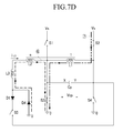
- FIG. 6 is a view illustrating signal timing of the sustain discharge driving circuit so as to generate the driving waveform in FIG. 4. FIGs. 7A to 7D are simplified views illustrating the operation of the sustain discharge driving circuit in FIG. 5 according to the signal timing in FIG. 6. First, assuming that transistors S1 and S4 are turned on before a
mode 1 starts, and transistors S2, S3, S5, and S6 are turned off, a voltage Vcp that is applied between the first and second ends of the panel capacitor Cp is maintained at the voltage Vs. Further, it is assumed that a voltage of the X electrodes of the panel capacitor Cp is higher than a voltage of the Y electrodes thereof by the voltage Vcp. Further, for a current lL3 that flows through the inductor L3, it is assumed that a direction of the current lL3 that flows from the inductor L3 toward the secondary coil L2 is a positive (+) direction. - Referring to FIGs. 6 and 7A, in a mode 1 (t0 ≤ t ≤ t1), the transistors S1 and S4 are turned off, and the transistor S5 is turned on. As shown in FIG. 7A, a resonance occurs in a path of the X electrodes of the panel capacitor Cp, the secondary coil L2, the inductor L3, the diode D1, the transistor S5, and the Y electrodes of the panel capacitor Cp (①).
- Further, a current path is formed by the X electrodes of the panel capacitor Cp, the primary coil L1, and the Y electrodes of the panel capacitor Cp (②).
- Next, in a mode 2 (t1 ≤ t ≤ t2), the transistors S2 and S3 are turned on. As shown in FIG. 7B, a current path of the transistor S2, the primary coil L1, the transistor S3, and the power supply Vs is formed (③). Then, a current path of the transistor S2, the secondary coil L2, the inductor L3, the diode D1, the diode D3, and the power supply Vs is formed (④). In addition, a current path of the transistor S5, the transistor S3, and the power supply Vs is formed (⑤), such that the voltage Vcp applied between the first and second ends of the panel capacitor Cp is maintained at a voltage -Vs.
- Accordingly, the discharge current flows through the transistor S3, the panel capacitor Cp, and the transistor S2. Since the current flowing through the panel capacitor Cp is shown as a current source, the current flowing through the panel capacitor Cp is equivalently illustrated as a current source coupled in parallel with the panel capacitor Cp.
- At this time, the size of the current lL3 flowing through the inductor L3 linearly decreases by the
current paths - Here, n denotes the number of turns of a secondary coil L2 when the number of turns of a primary coil L1 is equivalently set to be 1, as shown in FIG. 7A to FIG. 7D.
- Further, the voltage that is applied to the inductor becomes a voltage (n+1)Vs as shown in
Equation 2.
- Therefore, as shown in
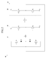
Equation 2, the higher the turn ratio 1:n of the coils that are wound around in the primary coil L1, and wound around in the secondary coil L2, is, the greater the voltage applied between the first and second ends of the inductor L3 is. Accordingly, the size of the current lL3 flowing through the inductor L3 reaches (or increases to) 0. - When the size of the current lL3 flowing through the inductor L3 becomes 0, in a mode 3 (t2 ≤ t ≤ t3), as shown in FIG. 7C, a current path of the diode D4, the diode D2 (not shown), the inductor L3, the secondary coil L2, and the transistor S2 is formed (⑥). At the same time, a current path of the power supply Vs, the transistor S3, the primary coil L1, and the transistor S2 is formed (⑦). At this time, as shown in FIGS. 6 and 7C, the size of the current |L3 of the inductor L3 is amplified by the primary coil L1 and secondary coil L2 that serve as the transformer, and linearly increases.
- Then, in a mode 4 (t3 ≤ t ≤ t4), the transistor S5 is turned off. As shown in FIGs. 6 and 7D, the size of current lL3 flowing through the inductor L3 linearly increases.
- When the
mode 4 finishes, the voltage of the panel capacitor Cp increases to the voltage Vs by the same methods of themodes 1 to 4, and then the voltage Vs is applied. - Further, when the primary coil L1 is connected in parallel to the panel capacitor Cp, a resonance frequency increases by (n+1) times. Therefore, it is possible for the voltage of the panel capacitor Cp to rise or fall at high speed.
- Also, as shown in FIG. 6, since the current lL3 flowing through the inductor L3 continuously increases, the power consumption is increased and thus efficiency is reduced.
- In order to address the above power consumption issue, a sustain discharge driving circuit according to a second exemplary embodiment of the present invention, as shown in FIG. 8, is provided.
- FIG. 8 is a view of the sustain discharge driving circuit according to the second exemplary embodiment of the present invention.
- As shown in FIG. 8, the sustain discharge driving circuit according to the second exemplary embodiment of the present invention includes a scan electrode driver 400' and a sustain electrode driver 500'.
- The scan electrode driver 400' includes a power recovery circuit 410' and a sustain voltage supply unit 420'. The sustain electrode driver 500' also includes a power recovery circuit 510' and a sustain voltage supply unit 520'.
- In FIG. 8, the sustain discharge driving circuit is similar to that in FIG. 5. It differs in that in the power recovery circuit 510' no diodes D3, D4 are provided which is why an additional power recovery circuit 410' is provided which is similar to the power recovery circuit 510'. The power recovery circuit 410' comprises a transistor S7 having a drain connected to a source of a transistor S8 and a source connected to a cathode of a diode D3. The diode D3 has an anode connected to a cathode of a diode D4 which has an anode connected to a drain of the transistor S8. The anode of the diode D3 connects to a first end of a primary coil L1 which has a second end connected to the sustain electrodes X of the panel capacitance Cp. The sustain voltage supply unit 420' and the sustain voltage supply unit 520' have the same structure as the sustain
voltage supply unit 420 and the sustainvoltage supply unit 520 of Fig. 5 with the only difference that the first end of the primary coil L1 is not connected to the source of transistor S3 and the drain of transistor S4. - An operation of the sustain discharge driving circuit shown in FIG. 8 will be described in more detail with reference to FIGs. 9, and 10A to 10D.
- FIG. 9 is a view illustrating signal timing of the sustain discharge driving circuit so as to generate the driving waveform in FIG. 4. FIGs. 10A to 10D are simplified views illustrating the operation of the sustain discharge driving circuit in FIG. 8 according to the signal timing in FIG. 9. First, assume that transistors S2 and S3 are turned on before a
mode 1 M1 starts, and the remaining transistors S1, S4, S5, S6, S7, and S8 are turned off, the voltage Vcp that is applied between the first and second ends of the panel capacitor Cp is maintained at the voltage -Vs. Like the first embodiment, it is assumed that the voltage of the X electrodes of the panel capacitor Cp is higher than the voltage applied to the Y electrodes thereof by the voltage Vs. - Referring to FIGs. 9 and 10A, in a mode 1 (t0 ≤ t ≤ t1), the transistors S6 and S8 are turned on. As shown in FIG. 10A, a path of the power supply Vs, the transistor S3, the transistor S8, the diode D4, the primary coil L1, the transistor S2, and the power supply 0V is formed (①).
- Further, a current path of the power supply Vs, the transistor S3, the transistor S6, the diode D2, the inductor L3, the secondary coil L2, the transistor S2, and the power supply 0V is formed (②).
- At this time, a current that is amplified by the primary coil L1 flows through the secondary coil L2, such that the amount of current stored in the inductor (or resonance inductor) L3 increases. Therefore, the current lo that is stored in the inductor L3 is represented in
Equation 3.
- Therefore, as shown in FIG. 9, the current lL3 flowing through the inductor L3 is linearly increased by the current lo. The building up of the current lL3 in the
mode 1 is for suppressing the occurrence of hard switching when the sustain voltage is applied by allowing the voltage (which is rising) to reach the voltage Vs, in consideration of the parasitic component that appears in the actual circuit, a voltage drop, and the like. - Next, the transistors S2 and S3 are turned off in a mode 2 (t1 ≤ t ≤ t2). As shown in FIG. 10B, a resonance occurs in a path of the Y electrodes of the panel capacitor Cp, the transistor S6, the diode D2, the inductor L3, the secondary coil L2, and the X electrodes of the panel capacitor Cp (③). As the current stored in the inductor L3 is supplied to the panel capacitor Cp, the voltage Vcp applied between the first and second ends of the panel capacitor Cp increases from the voltage -Vs to the voltage Vs.
- In addition, a path of the Y electrodes of the panel capacitor Cp, the transistor S8, the diode D4, the primary coil L1, and the X electrodes of the panel capacitor Cp is formed (④).
- At this time, according to the
current path ③, a circuit equation can be expressed as shown inEquation 4.
Equation 4, it is possible to obtain a value Vcp as shown inEquation 5.
- As shown in
Equation 5, since a frequency of the voltage Vcp becomes (n+1)ω0, the frequency increases (n+1) times more than the resonance frequency as shown inEquation 1, such that a resonance period is reduced. Accordingly, the second exemplary embodiment of the present invention can dramatically reduce the rising period or the falling period of the voltage of the panel capacitor Cp. - Then, in a mode 3 (t2 ≤ t ≤ t3), the transistors S1 and S4 are turned on. As shown in FIG. 10C, a current path of the power supply Vs, the transistor S1, the panel capacitor Cp, the transistor S4, and the power supply 0V is formed (⑤), such that the voltage Vcp applied between the first and second ends of the panel capacitor Cp is maintained at the voltage Vs.
- Also, the size of the current lL3 flowing through the inductor L3 is linearly reduced as shown in
Equation 6.
- When the size of the current lL3 flowing through the inductor L3 becomes 0, as shown in FIG. 10D, in a mode 4 (t3≤ t ≤ t4), the transistors S6 and S8 are turned off and thus only a current path (⑤) is formed. Here, discharge current flows through the transistor S1, the panel capacitor Cp, the transistor S4 and ground. Therefore, in the
mode 4, the current does not flow through the inductor L3. That is, unlike the first exemplary embodiment of the present invention, according to the second exemplary embodiment of the present invention, the current only flows through the inductor L3 during the rising period or the falling period of the voltage of the panel capacitor Cp, and the current does not flow through the inductor L3 when the voltage Vs is applied. - Therefore, unlike the first exemplary embodiment of the present invention, the current does not flow through the inductor L3 when the voltage Vs or the voltage -Vs is applied, thereby reducing power consumption.
- Further, when the
mode 4 finishes in the second exemplary embodiment of the present invention, the voltage of the panel capacitor Cp increases to the voltage -Vs according to substantially the same methods as that of themodes 1 to 4, and the voltage -Vs is applied. - As described above, according to certain embodiments of the present invention, a sustain discharge driving circuit includes a primary coil of a transformer that is connected in parallel to a panel capacitor serving as a capacitive load such that the rising period and the falling period of the voltage applied between the first and second ends of the panel capacitor are reduced. As a result, the time, during which the switch is turned on, is reduced, and the power consumption is reduced. Further, when the sustain voltage is alternately applied, the current is initially applied to the inductor and energy stored in the inductor is used, such that the occurrence of hard switching when the sustain voltage is applied is reduced to thereby protect elements of the circuit, and the power consumption during the sustain discharge can be further reduced.
Claims (9)
- A plasma display comprising:a first power supply for providing a first supply voltage;a second power supply for providing a second supply voltage;a panel comprising a plurality of first electrodes and a plurality of second electrodes;a first electrode driver connected to the first electrodes and adapted to drive the first electrodes;a second electrode driver connected to the second electrodes and adapted to drive the second electrodes;a power recovery circuit; anda transformer comprising a primary coil having a first end connected to the first electrodes and a second end connected to a first terminal of the power recovery circuit; anda secondary coil having a first end connected to the first end of the primary coil and a second end connected to a second terminal of the power recovery circuit.
- The plasma display of claim 1, wherein the first electrode driver comprises a first transistor having a drain connected to the first power supply and a source connected to a drain of a second transistor, the second transistor having a source connected to the second power supply, and
wherein the second electrode driver comprises a third transistor having a drain connected to the first power supply and a source connected to a drain of a fourth transistor, the fourth transistor having a source connected to the second power supply. - The plasma display of one of claims 1 or 2, wherein the power recovery circuit comprises a first diode, a second diode, a fifth transistor, a sixth transistor and an inductor,
wherein the inductor has a first end connected to the second terminal of the power recovery circuit and a second end connected to an anode of the first diode and to a cathode of the second diode,
wherein the first diode has a cathode connected to a source of the fifth transistor,
wherein the second diode has an anode connected to a drain of the sixth transistor, and
wherein a drain of the fifth transistor is connected to a source of the sixth transistor and to the second electrodes. - The plasma display of claim 3, wherein the drain of the fifth transistor and the source of the sixth transistor are connected to the first terminal of the power recovery circuit and wherein the power recovery circuit further comprises a third diode having an anode connected to the source of the fifth transistor and a cathode connected to the first power supply and a fourth diode having an anode connected to the second power supply and a cathode connected to the drain of the sixth transistor.
- The plasma display of claim 4, wherein the second end of the primary coil is connected the second electrodes.
- The plasma display of one of claims 4 or 5, comprising a controller adapted to
during a first mode of operation turn off the first and the fourth transistors and to turn on the fifth transistor;
during a second mode of operation turn on the second and the third transistors; and
during a third mode of operation switch off the fifth transistor. - The plasma display of claim 3, wherein the power recovery circuit further comprises a seventh transistor, an eighth transistor, a fifth diode, and a sixth diode, the seventh transistor having a drain connected to the drain of the fifth transistor and a source connected to a cathode of the fifth diode, the fifth diode having an anode connected to a cathode of the sixth diode and to the first terminal of the power recovery circuit, the sixth diode having an anode connected to a drain of the eighth transistor, the eight transistor having a source connected to the drain of the seventh transistor.
- The plasma display of claim 7, comprising a controller adapted to
during a first mode of operation turn on the sixth and the eighth transistors;
during a second mode of operation turn off the second and the third transistors;
during a third mode of operation turn on the first and the fourth transistors; and
during a fourth mode of operation turn off the sixth and the eighth transistors. - The plasma display of any of the preceding claims, wherein the primary coil comprises a first number of coils wound around the primary coil and wherein the secondary coil comprises a second number of coils wound around the secondary coil, the second number of coils being greater than the first number of coils.
Applications Claiming Priority (1)
| Application Number | Priority Date | Filing Date | Title |
|---|---|---|---|
| KR1020060050056A KR100749489B1 (en) | 2006-06-02 | 2006-06-02 | Plasma Display and Driving Device |
Publications (2)
| Publication Number | Publication Date |
|---|---|
| EP1863000A2 true EP1863000A2 (en) | 2007-12-05 |
| EP1863000A3 EP1863000A3 (en) | 2007-12-12 |
Family
ID=38535597
Family Applications (1)
| Application Number | Title | Priority Date | Filing Date |
|---|---|---|---|
| EP07109261A Withdrawn EP1863000A3 (en) | 2006-06-02 | 2007-05-31 | Plasma display and driving device thereof |
Country Status (5)
| Country | Link |
|---|---|
| US (1) | US20070279405A1 (en) |
| EP (1) | EP1863000A3 (en) |
| JP (1) | JP2007323065A (en) |
| KR (1) | KR100749489B1 (en) |
| CN (1) | CN100520881C (en) |
Cited By (1)
| Publication number | Priority date | Publication date | Assignee | Title |
|---|---|---|---|---|
| EP2200009A1 (en) | 2008-12-15 | 2010-06-23 | Samsung SDI Co., Ltd. | Energy recovery circuit for a plasma display |
Families Citing this family (4)
| Publication number | Priority date | Publication date | Assignee | Title |
|---|---|---|---|---|
| JPWO2009130860A1 (en) * | 2008-04-22 | 2011-08-11 | パナソニック株式会社 | Plasma display apparatus and driving method of plasma display panel |
| US9714759B2 (en) * | 2009-11-02 | 2017-07-25 | City University Of Hong Kong | Apparatus or circuit for driving a DC powered lighting equipment |
| CN103345899A (en) * | 2013-07-01 | 2013-10-09 | 四川虹欧显示器件有限公司 | Plasma display screen driving method reducing low discharge and promoting energy efficiency |
| CN110021259B (en) * | 2018-03-23 | 2020-12-22 | 京东方科技集团股份有限公司 | Power supply voltage supply circuit, method, display substrate and display device |
Family Cites Families (11)
| Publication number | Priority date | Publication date | Assignee | Title |
|---|---|---|---|---|
| JPH07261701A (en) * | 1994-03-20 | 1995-10-13 | Fujitsu Ltd | Capacitive load driving circuit and driving method thereof |
| JP2755201B2 (en) * | 1994-09-28 | 1998-05-20 | 日本電気株式会社 | Drive circuit for plasma display panel |
| US6160531A (en) * | 1998-10-07 | 2000-12-12 | Acer Display Technology, Inc. | Low loss driving circuit for plasma display panel |
| KR100456680B1 (en) * | 2002-01-11 | 2004-11-10 | 재단법인서울대학교산학협력재단 | Driving circuit for energy recovery in plasma display panel |
| KR20030066422A (en) * | 2002-01-30 | 2003-08-09 | 문건우 | Driver Circuit and Power Supply for Plasma Display Penel(PDP) |
| KR100502350B1 (en) * | 2003-04-25 | 2005-07-20 | 삼성에스디아이 주식회사 | Energy recovery circuit of plasma display panel and driving apparatus therewith |
| KR100574364B1 (en) * | 2003-09-18 | 2006-04-27 | 엘지전자 주식회사 | Energy recovery device and method of plasma display panel |
| US20050088376A1 (en) * | 2003-10-28 | 2005-04-28 | Matsushita Electric Industrial Co., Ltd. | Capacitive load driver and plasma display |
| JP2005196131A (en) | 2003-10-28 | 2005-07-21 | Matsushita Electric Ind Co Ltd | Capacitive load driving device and plasma display equipped with the same |
| US20050190125A1 (en) * | 2004-02-23 | 2005-09-01 | Matsushita Electric Industrial Co. Ltd. | Capacitive load driver and plasma display |
| JP2005338582A (en) * | 2004-05-28 | 2005-12-08 | Matsushita Electric Ind Co Ltd | Capacitive load driving device and plasma display equipped with the same |
-
2006
- 2006-06-02 KR KR1020060050056A patent/KR100749489B1/en not_active Expired - Fee Related
-
2007
- 2007-03-16 US US11/687,586 patent/US20070279405A1/en not_active Abandoned
- 2007-05-16 JP JP2007130725A patent/JP2007323065A/en active Pending
- 2007-05-31 EP EP07109261A patent/EP1863000A3/en not_active Withdrawn
- 2007-06-01 CN CNB2007101054808A patent/CN100520881C/en not_active Expired - Fee Related
Cited By (1)
| Publication number | Priority date | Publication date | Assignee | Title |
|---|---|---|---|---|
| EP2200009A1 (en) | 2008-12-15 | 2010-06-23 | Samsung SDI Co., Ltd. | Energy recovery circuit for a plasma display |
Also Published As
| Publication number | Publication date |
|---|---|
| US20070279405A1 (en) | 2007-12-06 |
| CN101083046A (en) | 2007-12-05 |
| KR100749489B1 (en) | 2007-08-14 |
| JP2007323065A (en) | 2007-12-13 |
| EP1863000A3 (en) | 2007-12-12 |
| CN100520881C (en) | 2009-07-29 |
Similar Documents
| Publication | Publication Date | Title |
|---|---|---|
| US20030080925A1 (en) | Plasma display panel, and apparatus and method for driving the same | |
| US7379033B2 (en) | Plasma display device and driving method of plasma display panel | |
| US7307601B2 (en) | Driving method and device of plasma display panel and plasma display device | |
| CN100520881C (en) | Plasma display and driving device thereof | |
| US20080117131A1 (en) | Plasma display device | |
| US7495635B2 (en) | Plasma display device and driving method for plasma display panel | |
| CN101149898B (en) | Plasma display and apparatus and method of driving the plasma display | |
| KR100732583B1 (en) | Plasma display apparatus | |
| KR100658636B1 (en) | Plasma display device, driving device thereof and driving method thereof | |
| KR100670153B1 (en) | Plasma display device, driving device thereof and driving method thereof | |
| KR100454025B1 (en) | Plasma display panel and driving apparatus thereof and driving method thereof | |
| EP1981016A1 (en) | Plasma display and driving device thereof | |
| KR100658635B1 (en) | Plasma display device, driving device thereof and driving method thereof | |
| US20080055198A1 (en) | Method of driving plasma display device for reducing power consumption | |
| KR100658634B1 (en) | Plasma display device, driving device thereof and driving method thereof | |
| KR100649191B1 (en) | Plasma display device and driving method thereof | |
| KR100823493B1 (en) | Plasma display device and driving method thereof | |
| JP2009122649A (en) | Plasma display device and driving device and driving method thereof | |
| EP2113902A2 (en) | Plasma display device and driving method thereof | |
| EP1783731A2 (en) | Plasma display device, driving apparatus and driving method thereof | |
| US20070120773A1 (en) | Plasma display device, and apparatus and method for driving the same | |
| KR20080006348A (en) | Plasma display device, driving device thereof and driving method thereof | |
| US20070120532A1 (en) | Driving device and method of driving plasma displays | |
| KR20080040503A (en) | Plasma display device, driving device thereof and driving method thereof | |
| KR20080026364A (en) | Plasma Display, Driving Device and Driving Method |
Legal Events
| Date | Code | Title | Description |
|---|---|---|---|
| PUAI | Public reference made under article 153(3) epc to a published international application that has entered the european phase |
Free format text: ORIGINAL CODE: 0009012 |
|
| PUAL | Search report despatched |
Free format text: ORIGINAL CODE: 0009013 |
|
| 17P | Request for examination filed |
Effective date: 20070531 |
|
| AK | Designated contracting states |
Kind code of ref document: A2 Designated state(s): AT BE BG CH CY CZ DE DK EE ES FI FR GB GR HU IE IS IT LI LT LU LV MC MT NL PL PT RO SE SI SK TR |
|
| AX | Request for extension of the european patent |
Extension state: AL BA HR MK YU |
|
| AK | Designated contracting states |
Kind code of ref document: A3 Designated state(s): AT BE BG CH CY CZ DE DK EE ES FI FR GB GR HU IE IS IT LI LT LU LV MC MT NL PL PT RO SE SI SK TR |
|
| AX | Request for extension of the european patent |
Extension state: AL BA HR MK YU |
|
| AKX | Designation fees paid |
Designated state(s): DE FR GB |
|
| STAA | Information on the status of an ep patent application or granted ep patent |
Free format text: STATUS: THE APPLICATION HAS BEEN WITHDRAWN |
|
| 18W | Application withdrawn |
Effective date: 20100624 |