EP1858053A2 - Plasmaanzeigetafel und Herstellungsverfahren dafür - Google Patents
Plasmaanzeigetafel und Herstellungsverfahren dafür Download PDFInfo
- Publication number
- EP1858053A2 EP1858053A2 EP07103864A EP07103864A EP1858053A2 EP 1858053 A2 EP1858053 A2 EP 1858053A2 EP 07103864 A EP07103864 A EP 07103864A EP 07103864 A EP07103864 A EP 07103864A EP 1858053 A2 EP1858053 A2 EP 1858053A2
- Authority
- EP
- European Patent Office
- Prior art keywords
- dielectric layer
- glass
- film thickness
- substrate
- electrodes
- Prior art date
- Legal status (The legal status is an assumption and is not a legal conclusion. Google has not performed a legal analysis and makes no representation as to the accuracy of the status listed.)
- Withdrawn
Links
Images


Classifications
-
- H—ELECTRICITY
- H01—ELECTRIC ELEMENTS
- H01J—ELECTRIC DISCHARGE TUBES OR DISCHARGE LAMPS
- H01J11/00—Gas-filled discharge tubes with alternating current induction of the discharge, e.g. alternating current plasma display panels [AC-PDP]; Gas-filled discharge tubes without any main electrode inside the vessel; Gas-filled discharge tubes with at least one main electrode outside the vessel
- H01J11/20—Constructional details
- H01J11/22—Electrodes, e.g. special shape, material or configuration
- H01J11/24—Sustain electrodes or scan electrodes
-
- H—ELECTRICITY
- H01—ELECTRIC ELEMENTS
- H01J—ELECTRIC DISCHARGE TUBES OR DISCHARGE LAMPS
- H01J11/00—Gas-filled discharge tubes with alternating current induction of the discharge, e.g. alternating current plasma display panels [AC-PDP]; Gas-filled discharge tubes without any main electrode inside the vessel; Gas-filled discharge tubes with at least one main electrode outside the vessel
- H01J11/10—AC-PDPs with at least one main electrode being out of contact with the plasma
- H01J11/12—AC-PDPs with at least one main electrode being out of contact with the plasma with main electrodes provided on both sides of the discharge space
-
- H—ELECTRICITY
- H01—ELECTRIC ELEMENTS
- H01J—ELECTRIC DISCHARGE TUBES OR DISCHARGE LAMPS
- H01J11/00—Gas-filled discharge tubes with alternating current induction of the discharge, e.g. alternating current plasma display panels [AC-PDP]; Gas-filled discharge tubes without any main electrode inside the vessel; Gas-filled discharge tubes with at least one main electrode outside the vessel
- H01J11/20—Constructional details
- H01J11/34—Vessels, containers or parts thereof, e.g. substrates
- H01J11/38—Dielectric or insulating layers
-
- H—ELECTRICITY
- H01—ELECTRIC ELEMENTS
- H01J—ELECTRIC DISCHARGE TUBES OR DISCHARGE LAMPS
- H01J9/00—Apparatus or processes specially adapted for the manufacture, installation, removal, maintenance of electric discharge tubes, discharge lamps, or parts thereof; Recovery of material from discharge tubes or lamps
- H01J9/02—Manufacture of electrodes or electrode systems
-
- H—ELECTRICITY
- H01—ELECTRIC ELEMENTS
- H01J—ELECTRIC DISCHARGE TUBES OR DISCHARGE LAMPS
- H01J2211/00—Plasma display panels with alternate current induction of the discharge, e.g. AC-PDPs
- H01J2211/20—Constructional details
- H01J2211/22—Electrodes
- H01J2211/225—Material of electrodes
-
- H—ELECTRICITY
- H01—ELECTRIC ELEMENTS
- H01J—ELECTRIC DISCHARGE TUBES OR DISCHARGE LAMPS
- H01J2211/00—Plasma display panels with alternate current induction of the discharge, e.g. AC-PDPs
- H01J2211/20—Constructional details
- H01J2211/22—Electrodes
- H01J2211/24—Sustain electrodes or scan electrodes
- H01J2211/245—Shape, e.g. cross section or pattern
Definitions
- This invention relates to a structure and a manufacturing method of a plasma display panel (hereinafter, referred to as "PDP"), and more particularly, relates to a structure and a manufacturing method of a PDP that causes no bubbles in a dielectric layer of a glass material used for covering metal electrodes.
- PDP plasma display panel
- An AC drive three-electrode face discharge type PDP has been known as a conventional PDP.
- This PDP has a structure in which a number of display electrodes capable of face discharging are placed in a horizontal direction on the inner face of a substrate on the front face side, and a number of address electrodes used for selecting a light-emitting cell are placed on the inner face of a substrate on the back face side, with an intersection between each display electrode and each address electrode serving as one cell (unit light-emitting area).
- One pixel is constituted by three cells, that is, a red color (R) cell, a green color (G) cell and a blue color (B) cell.
- the substrate on the front face side and the substrate on the back face side, thus formed, are placed face to face with each other with the peripheral portion being sealed, and the inside thereof is then filled with a discharge gas so that the PDP is manufactured.
- a plurality of display electrodes are formed on a glass substrate.
- These display electrodes are normally constituted by transparent electrodes and metal electrodes.
- the transparent electrodes are formed by film-forming ITO, SnO 2 or the like on the substrate and by patterning the resulting film.
- the metal electrodes are used for reducing the wiring resistance of the electrodes, and also referred to as bus electrodes.
- the metal electrodes are formed as metal electrodes having a three-layer structure through processes in which metal films of three layers of Cr-Cu-Cr are formed on the transparent electrodes and the resulting films are patterned. Alternatively, a silver paste is applied onto the transparent electrodes and then subjected to a firing process so that the metal electrodes are formed.
- a dielectric layer is formed on the display electrodes, and a protective layer is then formed thereon.
- address electrodes made of metal are formed on a glass substrate in a direction crossing the display electrodes, and a dielectric layer is formed thereon, with barrier ribs being formed thereon, and a phosphor layer is then formed in an elongated recess groove between the barrier ribs.
- a low-melting-point glass containing lead is normally used because of its easiness in processability (see Japanese Unexamined Patent Publication No. Hei 6(1994)-33503 ).
- the present invention has been devised so as to solve the above-mentioned problems, and upon placing a glass material on metal electrodes and carrying out a firing process so that a dielectric layer is formed, by taking the thickness of the electrodes and the thickness of the dielectric layer into consideration, the generation of bubbles due to a reaction between the metal electrodes and glass is restrained to prevent bubbles from remaining in the dielectric layer; thus, even a non-lead-based glass material can be used upon forming the dielectric layer, and it becomes possible to improve performances of the manufactured panel.
- the present invention provides a plasma display panel that is provided with a substrate, a plurality of metal electrodes formed on the substrate in a predetermined direction and a dielectric layer that is formed on the metal electrodes by firing a glass material, and in this structure, the metal electrodes are formed with a film thickness of 6 ⁇ m or less, and the dielectric layer is formed with a film thickness of 25 ⁇ m or less.
- examples of the substrate include substrates of materials such as glass, quartz and ceramics, as well as any of these substrates on which a desired structure such as electrodes, an insulating film, a dielectric layer, a protective film and the like are formed.
- a plurality of metal electrodes may be formed on the substrate in a predetermined direction.
- These metal electrodes can be formed by using various known materials through known methods in the corresponding field.
- the materials used for the electrodes examples thereof include metal conductive materials such as Ag, Au, Al, Cu and Cr.
- the forming method of the electrodes various conventionally known methods in the corresponding field may be used. For example, a thick-film forming technique such as printing may be used to form the electrodes, or a thin-film forming technique corresponding to a physical deposition method or a chemical deposition method may be used. As an example of the thick-film forming technique, a screen printing method is used.
- Examples of the physical deposition method as the thin-film forming technique include a vapor deposition method, a sputtering method and the like.
- Examples of the chemical deposition method include a thermal CVD method, a photo CVD method and a plasma CVD method.
- the dielectric layer may be formed through processes in which a glass material is placed on a metal electrode and this is then fired.
- This dielectric layer is formed by applying a glass paste made from non-lead-type glass flit (glass powder), a binder resin and a solvent onto a substrate in a manner so as to cover the metal electrodes through a screen printing method, or by affixing a green sheet (un-sintered dielectric sheet) of non-lead-type glass powder thereto and firing the resulting substrate.
- glass materials used as the non-lead-type glass flit include B 2 O 3 -SiO 2 -ZnO-based glass, Bi 2 O 3 -B 2 O 3 -SiO 2 -based glass, B 2 O 3 -SiO 2 -Al 2 O 3 -based glass, ZnO-B 2 O 3 -SiO 2 -BaO-based glass, and any of the foregoing glass materials mixed with an alkali or alkali-earth oxide.
- the dielectric layer may be formed by laminating a plurality of dielectric layers into, for example, double layers and triple layers.
- a first dielectric layer is formed with a film thickness of 12 ⁇ m or less and a second dielectric layer may be formed thereon with a film thickness of 13 ⁇ m or less.
- the metal electrodes may be such that a Cr layer is formed on a substrate, a Cu layer is formed thereon, and a Cr layer is further formed thereon respectively through a vapor film-forming method, and a resist film is formed on the metal film with the three layers, and after having patterned the resist film by using a photolithographic technique, the metal film on unnecessary portions are removed by etching so that a metal electrode having a three-layer-structure of Cr-Cu-Cr is prepared.
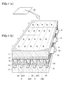
- Figs. 1(a) and 1(b) are explanatory diagrams that show a structure of a PDP manufactured by a manufacturing method of the present invention.
- Fig. 1(a) shows the entire structure of the PDP
- Fig. 1(b) is a partially exploded perspective view of the PDP.
- This PDP is a three-electrode face discharge type PDP of an AC drive type for color display.
- the PDP 10 is constituted by a substrate 11 on the front face side on which constituent elements that provide functions as the PDP are formed and a substrate 21 on the back face side.
- a substrate 11 on the front face side and the substrate 21 on the back face side for example, a glass substrate, a quartz substrate and a ceramics substrate may be used.
- Display electrodes X and display electrodes Y are placed with equal intervals in the horizontal direction on the inner side face of the substrate 11 on the front face side. All the gaps between the adjacent display electrodes X and display electrodes Y form display lines L.
- Each of the display electrodes X and Y is constituted by a transparent electrode 12 with a wide width, made of ITO, SnO 2 or the like, and a bus electrode 13 with a narrow width, made of metal, such as Ag, Au, Al, Cu, Cr or a laminated body thereof (for example, Cr-Cu-Cr laminated structure), or the like.
- a thick-film forming technique such as screen printing may be used, and in the case of other materials, a thin-film forming technique such as a vapor method and a sputtering method and an etching technique may be used, so that the display electrodes having a desired number, thickness, width and intervals are formed.
- the display electrodes X and Y may be made of only metal, such as Ag, Au, Al, Cu, Cr or a laminated body thereof.
- the form of the metal electrode has a line pattern or a mesh pattern so that light from phosphor layers is effectively transmitted.
- a PDP having a so-called ALIS structure in which the display electrodes X and the display electrodes Y are placed with equal intervals, with all the gaps between the adjacent display electrodes X and display electrodes Y forming display lines L, is shown.
- the present invention may be applied even to a PDP having a structure in which paired display electrodes X and Y are placed with a gap (non-discharging gap) causing no discharge.
- a dielectric layer 17 is formed on the display electrodes X and Y in a manner so as to cover the display electrodes X and Y.
- the dielectric layer 17 is formed by applying a glass paste made from non-lead-type glass flit, a binder resin and a solvent onto a substrate 11 on the front face side through a screen printing method and by firing the resulting substrate.
- a protective layer 18 used for protecting the dielectric layer 17 from damage caused by collision of ions generated by a discharge upon displaying is formed on the dielectric layer 17.
- This protective film is made from MgO.
- the protective layer may be formed by using a known thin-film forming process in the corresponding field, such as an electron beam vapor deposition method and a sputtering method.
- a plurality of address electrodes A are formed on the inner side face of the substrate 21 on the back face side in a direction crossing the display electrodes X and Y when viewed from above, and a dielectric layer 24 is formed so as to cover the address electrodes A.
- Each of the address electrodes A is used for generating an address discharge so as to select a light-emitting cell at an intersection with the Y electrode, and formed into a three-layer structure of Cr-Cu-Cr.
- the address electrodes A may be formed by using another material such as Ag, Au, Al, Cu, or Cr.
- a thick-film forming technique such as screen printing may be used, and in the case of the other materials, a thin-film forming technique such as a vapor method and a sputtering method and an etching technique may be used, so that the address electrodes having a desired number, thickness, width and intervals are formed.
- the dielectric layer 24 may be formed by using the same material and the same method as the dielectric layer 17.
- a plurality of barrier ribs 29 having a stripe pattern are formed on the dielectric layer 24 between the adjacent address electrodes A.
- a mesh shape (box shape) in which discharge spaces are separated for each cell may be used.
- the barrier ribs 29 may be formed by using a method such as a sand blasting method, a printing method and a photo-etching method.
- the sand blasting method after a glass paste, made from low-melting-point glass flit, a binder resin, a solvent and the like, have been applied to the dielectric layer 24 and dried thereon, cutting particles are blown onto the glass paste layer with a cutting mask having openings of the barrier rib pattern attached thereon, so that the glass paste layer exposed to the openings of the mask is cut; thus, the resulting layer is fired to form the barrier ribs.
- a photosensitive resin is used as the binder resin, and after exposing and developing processes by using a mask, the resulting layer is fired to firm the barrier ribs.
- Phosphor layers of 28R, 28G and 28B having respective red (R), green (G) and blue (B) colors are formed on side faces and a bottom face of each of discharge spaces having a recess groove shape between the barrier ribs 29.
- Each of the phosphor layers 28R, 28G and 28B is formed through processes in which: a phosphor paste containing phosphor powder, a binder resin and a solvent has been applied to the discharge space having the recess groove shape between the barrier ribs 29 by using a screen printing method or a method using a dispenser, and after repeating this process for each of the colors, the resulting layers are fired.
- These phosphor layers 28R, 28G and 28B may also be formed through a photolithographic technique by using a sheet-shaped phosphor layer material (so-called green sheet) containing phosphor powder, a photosensitive material and a binder resin.
- a sheet having a desired color is affixed to the entire face of a display area on the substrate, and this is exposed and developed, and by repeating these processes for each of the colors, the phosphor layers of the respective colors are formed on the corresponding gaps between the barrier ribs.
- the substrate 11 on the front face side on which these constituent elements have been formed and the substrate 21 on the back face side are placed face to face with each other so that the display electrodes X and Y cross the address electrodes A, and the peripheral portion is sealed so that a discharge space 30 surrounded by the barrier ribs 29 is filled with a discharge gas in which Xe, Ne and the like are mixed; thus, a PDP is manufactured.
- the discharge space 30, located each of the intersections between the display electrodes X and Y and the address electrodes A forms one cell (unit light-emitting area) that is the minimum unit for display.
- One pixel is constituted by three cells of R, G and B.
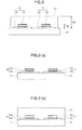
- Fig. 2 is a partial cross-sectional view showing a substrate on the front face side.
- the display electrodes X and Y are formed on the glass substrate 11 on the front face side.
- the display electrodes X (X electrodes) and the display electrodes Y (Y electrodes) have the same structure, that is, the structure in which bus electrodes 12 made of metal are formed on a transparent electrode 11.
- the transparent electrode 11 is formed with a film thickness in a range from 500 to 2000 ⁇ .
- the bus electrode 12 has a three-layer structure of Cr-Cu-Cr in which Cr has a film thickness in a range from 500 to 2000 ⁇ , with Cu being formed with a thickness of about 3 ⁇ m. Therefore, the thickness TE of each of the display electrodes X and Y is in an approximate range from 3 to 4 ⁇ m.
- a dielectric layer 17 is formed on the display electrodes X and Y. The thickness TD of the dielectric layer 17 is about 20 ⁇ m.
- Figs. 3 (a) and 3(b) are explanatory diagrams showing a first example of a manufacturing method of the substrate on the front face side.
- the substrate on the front face side is manufactured in the following processes.
- a transparent conductive film made of ITO, is formed on a glass substrate 11 by a method, such as a vapor deposition method and a sputtering method, and the transparent conductive film is patterned by using a photolithographic technique to prepare a transparent electrode 12.
- a three-layer metal conductive film of Cr-Cu-Cr is formed on the transparent electrode 12 by using a method such as a vapor deposition method and a sputtering method, and a resist film is formed on the metal conductive film, and after the resist film has been patterned by using the photolithographic technique, unnecessary portions of the metal conductive film are removed by etching so that bus electrodes 13 are formed.
- each of the display electrodes X and Y is formed with a thickness of 6 ⁇ m or less.
- the film thickness of the Cu portion of the bus electrode 13 is set to 3 to 4 ⁇ m.
- a glass paste (glass material), prepared by mixing a binder resin and a solvent with non-lead-based glass flit, is applied onto the glass substrate 11 so as to cover the display electrodes X and Y by using a screen printing method, and after this has been dried into a dried film, the glass substrate 11 is loaded into a firing furnace, and the dried film of the glass material is fired at a temperature in a range from 600 to 610°C so that a dielectric film 17 is formed (see Fig. 3(b)).
- the dielectric layer 17 is formed with a thickness of about 20 ⁇ m.
- the dielectric layer 17 may be formed by affixing a green sheet (un-sintered dielectric sheet) with which non-lead-based glass powder is mixed to the substrate 11 on the front face side, and by firing the resulting substrate.
- non-lead-based glass flit As the non-lead-based glass flit, one of the following is used:
- the glass material When the dried film of the glass material is fired, the glass material is fused. At this time, bubbles are generated in the glass material by an electrochemical reaction between the glass material and the bus electrodes 13 of metal. The generation of these bubbles is mainly caused by a chemical reaction between Cu and glass.
- Cu is not directly made in contact with the glass material because it is sandwiched by Cr.
- the three-layer metal conductive film of Cr-Cu-Cr is etched by a wet-etching process or the like, Cu is exposed between Cr and Cr, and the exposed Cu comes into contact with the glass material to cause a reaction, with the result that bubbles are generated in the glass material.
- the thickness of the bus electrode 13 that is a generation source of bubbles is made thinner.
- the thickness of Cu is made thinner. More specifically, as described earlier, the thickness of the bus electrode 13 is set to 6 ⁇ m or less, with the thickness of Cu being set to 3 to 4 ⁇ m.
- the film thickness of the dielectric layer 17 is made thinner. More specifically, as described above, the film thickness of the dielectric layer is set to 25 ⁇ m or less. With this arrangement, even when the flowability of the glass material is lowered because of the use of the non-lead-based glass material, generated bubbles are allowed to float and easily defoamed so that the bubbles in the dielectric layer 17 are reduced upon completion of the firing process.
- the thickness of the electrodes is made thinner to reduce the absolute amount of bubbles that are generated and the film thickness of the dielectric layer is also made thinner so as to easily release bubbles in the glass material so that bubbles in the dielectric layer 17 are reduced upon completion of the firing process.
- the discharge voltage between the display electrodes relates to the film thickness of the dielectric layer.
- the film thickness of the dielectric layer relates to the static capacitance of the dielectric layer.
- the static capacitance of the dielectric layer relates to the quantity of discharge between the display electrodes. Therefore, in an attempt to obtain an appropriate quantity of discharge by applying an appropriate discharge voltage across the display electrodes, the dielectric layer is preferably made so as to accumulate a charge of 0.2 nF or more per 1 cm 2 thereof, in the case when the film thickness of the dielectric layer is set to 25 ⁇ m or less.
- Figs. 4 (a) to 4(c) are explanatory diagrams that show a second example of the manufacturing method of the substrate on the front face side.
- the dielectric layer may be formed by laminating a plurality of dielectric layers. For example, two layers or three layers of the dielectric layers may be formed. In the case when two layers of the dielectric layers are formed, for example, the first dielectric layer is formed with a film thickness of 12 ⁇ m or less, and the second dielectric layer may be formed thereon with a film thickness of 13 ⁇ m or less.
- transparent electrodes 12 and bus electrodes 13 are formed on a glass substrate 11 on the front face side by using the same materials as those of the aforementioned first example through the same method (see Fig. 4(a)).
- the display electrodes X and Y are formed with a film thickness of 6 ⁇ m or less.
- the film thickness of the Cu portion of the bus electrode 13 is set in a range from 3 to 4 ⁇ m.
- the dielectric layer is formed through two-layer processes.
- a non-lead-based glass paste softening point: about 600°C
- the glass substrate 11 is loaded into a firing furnace, and the dried film of the glass material is fired at a temperature in a range from 600 to 610°C so that a first dielectric film 17a is formed with a thickness of 5 to 10 ⁇ m (see Fig. 4(b)).
- a non-lead-based glass paste (softening point: about 550°C) is applied onto the first dielectric film 17a after the firing process by using the screen printing method, and after this has been dried into a dried film, the resulting glass substrate is loaded into a firing furnace, and the dried film of the glass material is fired at a temperature in a range from 550 to 560°C so that a second dielectric film 17b is formed with a thickness of 10 to 15 ⁇ m (see Fig. 4(c)).
- the first dielectric layer 17a and the second dielectric layer 17b are formed so as to have a total thickness of about 20 ⁇ m.
- Fig. 5 is a Table indicating the relationship between the film thickness of the dielectric layer and the number of bubbles.
- Fig. 6 is a graph by which the Table of Fig. 5 is indicated.
- the film thickness of the dielectric layer is indicated as "dielectric film thickness”.
- a dielectric layer is formed by affixing a green sheet with which non-lead-based glass powder is mixed to a glass substrate on which display electrodes are formed with a thickness of 3 to 4 ⁇ m, and by firing the resulting substrate in a range from 600 to 610°C, a dielectric layer is formed so that the dielectric layer after the firing process is allowed to have a film thickness of 20 ⁇ m.
- the Table and Graph indicate the relationship between the film thickness ( ⁇ m) of the dielectric layer at this time and the number of bubbles (number).
- the solid line shows the number of bubbles having a size in a range from 5 to 10 ⁇ m in diameter
- the dot line shows the number of bubbles having a size of 10 ⁇ m or more in diameter.
- the display electrodes are formed with a thickness of 3 to 4 ⁇ m while the dielectric layer is formed with a film thickness of about 20 ⁇ m by using a non-lead-based glass material, it has been confirmed that no bubbles exist in the dielectric layer.
- a panel is formed by using this structure, it has been confirmed that no problems such as an insufficient insulation and a reduction in luminescence arise.
- the thickness of metal electrodes is made thinner (6 ⁇ m or less) and the film thickness of the dielectric layer is also made thinner (25 ⁇ m or less) so that it becomes possible to eliminate bubbles in the dielectric layer upon completion of the firing process.
Landscapes
- Engineering & Computer Science (AREA)
- Physics & Mathematics (AREA)
- Plasma & Fusion (AREA)
- Chemical & Material Sciences (AREA)
- Materials Engineering (AREA)
- Manufacturing & Machinery (AREA)
- Gas-Filled Discharge Tubes (AREA)
Applications Claiming Priority (1)
| Application Number | Priority Date | Filing Date | Title |
|---|---|---|---|
| JP2006135357A JP2007305528A (ja) | 2006-05-15 | 2006-05-15 | プラズマディスプレイパネルおよびその製造方法 |
Publications (2)
| Publication Number | Publication Date |
|---|---|
| EP1858053A2 true EP1858053A2 (de) | 2007-11-21 |
| EP1858053A3 EP1858053A3 (de) | 2009-08-26 |
Family
ID=38472941
Family Applications (1)
| Application Number | Title | Priority Date | Filing Date |
|---|---|---|---|
| EP07103864A Withdrawn EP1858053A3 (de) | 2006-05-15 | 2007-03-09 | Plasmaanzeigetafel und Herstellungsverfahren dafür |
Country Status (5)
| Country | Link |
|---|---|
| US (1) | US8231422B2 (de) |
| EP (1) | EP1858053A3 (de) |
| JP (1) | JP2007305528A (de) |
| KR (1) | KR100812221B1 (de) |
| CN (2) | CN101764017A (de) |
Families Citing this family (5)
| Publication number | Priority date | Publication date | Assignee | Title |
|---|---|---|---|---|
| WO2009087773A1 (ja) * | 2008-01-10 | 2009-07-16 | Hitachi, Ltd. | プラズマディスプレイパネルの製造方法及びプラズマディスプレイパネル用基板構体の製造方法 |
| KR20090093057A (ko) * | 2008-02-28 | 2009-09-02 | 삼성에스디아이 주식회사 | 플라즈마 디스플레이 패녈 |
| WO2010058445A1 (ja) * | 2008-11-20 | 2010-05-27 | 日立プラズマディスプレイ株式会社 | プラズマディスプレイパネル |
| WO2010116746A1 (ja) * | 2009-04-10 | 2010-10-14 | 株式会社日立製作所 | Cu-Al-Co系合金の電極・配線を具備した電子部品 |
| CN104198079A (zh) * | 2014-07-30 | 2014-12-10 | 肇庆爱晟电子科技有限公司 | 一种高精度高可靠快速响应热敏芯片及其制作方法 |
Family Cites Families (21)
| Publication number | Priority date | Publication date | Assignee | Title |
|---|---|---|---|---|
| JP3015093B2 (ja) * | 1990-10-22 | 2000-02-28 | 富士通株式会社 | プラズマディスプレイパネルおよびその製造方法 |
| JP3846636B2 (ja) * | 1995-05-26 | 2006-11-15 | 株式会社日立プラズマパテントライセンシング | プラズマディスプレイパネル及びその製造方法 |
| JP3778223B2 (ja) | 1995-05-26 | 2006-05-24 | 株式会社日立プラズマパテントライセンシング | プラズマディスプレイパネル |
| KR19980065367A (ko) | 1996-06-02 | 1998-10-15 | 오평희 | 액정표시소자용 백라이트 |
| JP2839484B2 (ja) * | 1997-03-19 | 1998-12-16 | 富士通株式会社 | 透明絶縁性被膜形成用低融点ガラス |
| KR100430664B1 (ko) * | 1997-10-03 | 2004-06-16 | 가부시끼가이샤 히다치 세이사꾸쇼 | 가스방전형표시장치의제조방법 |
| JPH11144623A (ja) * | 1997-11-05 | 1999-05-28 | Toray Ind Inc | プラズマディスプレイ用基板およびその製造方法 |
| JPH11233011A (ja) * | 1998-02-18 | 1999-08-27 | Fujitsu Ltd | Pdpパネルの製造方法 |
| KR100297362B1 (ko) * | 1998-08-05 | 2001-08-07 | 구자홍 | 플라즈마디스플레이패널의버스전극형성방법 |
| KR20000056654A (ko) * | 1999-02-24 | 2000-09-15 | 구자홍 | 플라즈마 디스플레이 패널 |
| KR100794076B1 (ko) * | 1999-06-04 | 2008-01-10 | 마츠시타 덴끼 산교 가부시키가이샤 | 가스방전 표시장치와 그 제조방법 |
| KR100308048B1 (ko) * | 1999-07-26 | 2001-11-01 | 구자홍 | 플라즈마 디스플레이 패널 |
| JP2001151532A (ja) * | 1999-11-19 | 2001-06-05 | Asahi Glass Co Ltd | 電極被覆用低融点ガラスおよびプラズマディスプレイ装置 |
| FR2805393A1 (fr) * | 2000-02-23 | 2001-08-24 | Thomson Plasma | Procede de realisation d'une couche dielectrique sur un substrat en verre recouvert d'electrodes conductrices |
| JP2003045322A (ja) * | 2002-05-29 | 2003-02-14 | Matsushita Electric Ind Co Ltd | プラズマディスプレイパネルの製造方法 |
| JP4122875B2 (ja) * | 2002-07-17 | 2008-07-23 | 松下電器産業株式会社 | プラズマディスプレイパネルの製造方法 |
| US20040138045A1 (en) | 2002-08-26 | 2004-07-15 | Nippon Electric Glass Co. Ltd. | Dielectric material for a plasma display panel |
| KR100495488B1 (ko) | 2002-12-07 | 2005-06-16 | 엘지마이크론 주식회사 | 플라즈마 디스플레이 패널의 후면판 |
| JP4195997B2 (ja) * | 2003-11-17 | 2008-12-17 | パナソニック株式会社 | プラズマディスプレイパネルおよびその製造方法 |
| KR20050075528A (ko) * | 2004-01-15 | 2005-07-21 | 엘지전자 주식회사 | 플라즈마 디스플레이 패널 소자 및 그 제조 방법 |
| US20050242725A1 (en) * | 2004-04-26 | 2005-11-03 | Shinya Hasegawa | Glass composition and paste composition suitable for a plasma display panel, and plasma display panel |
-
2006
- 2006-05-15 JP JP2006135357A patent/JP2007305528A/ja active Pending
-
2007
- 2007-03-06 US US11/714,166 patent/US8231422B2/en not_active Expired - Fee Related
- 2007-03-09 EP EP07103864A patent/EP1858053A3/de not_active Withdrawn
- 2007-04-02 KR KR1020070032438A patent/KR100812221B1/ko not_active Expired - Fee Related
- 2007-04-05 CN CN201010002914A patent/CN101764017A/zh active Pending
- 2007-04-05 CN CN2007100958311A patent/CN101075524B/zh not_active Expired - Fee Related
Also Published As
| Publication number | Publication date |
|---|---|
| EP1858053A3 (de) | 2009-08-26 |
| CN101075524A (zh) | 2007-11-21 |
| KR100812221B1 (ko) | 2008-03-13 |
| US20070262716A1 (en) | 2007-11-15 |
| US8231422B2 (en) | 2012-07-31 |
| KR20070110770A (ko) | 2007-11-20 |
| JP2007305528A (ja) | 2007-11-22 |
| CN101764017A (zh) | 2010-06-30 |
| CN101075524B (zh) | 2011-04-13 |
Similar Documents
| Publication | Publication Date | Title |
|---|---|---|
| US8231422B2 (en) | Plasma display panel and manufacturing method thereof | |
| JP2004164885A (ja) | プラズマディスプレイパネルおよびその製造方法 | |
| JP2004273265A (ja) | プラズマディスプレイパネル | |
| US20040239246A1 (en) | Plasma display panel, plasma display displaying device and production method of plasma display panel | |
| US20080079365A1 (en) | Plasma display panel and manufacturing method thereof | |
| JP4375113B2 (ja) | プラズマディスプレイパネル | |
| US20080153378A1 (en) | Method of forming barrier ribs | |
| CN100452277C (zh) | 等离子显示板及其制造方法 | |
| JPH0765729A (ja) | プラズマディスプレイパネル及びその製造方法 | |
| CN101154549B (zh) | 等离子体显示面板 | |
| JP4186504B2 (ja) | プラズマディスプレイパネル | |
| JP4508282B2 (ja) | プラズマディスプレイパネル | |
| US20080116802A1 (en) | Plasma display panel and method of forming a barrier rib thereof | |
| US20090167175A1 (en) | Plasma display panel | |
| US20090026950A1 (en) | Plasma display panel | |
| US20080157670A1 (en) | Plasma display panel and method of manufacturing the same | |
| JP2005135831A (ja) | プラズマディスプレイパネル | |
| JP2007234282A (ja) | プラズマディスプレイパネルおよびその製造方法 | |
| JPWO2008015729A1 (ja) | プラズマディスプレイパネルおよびその製造方法 | |
| WO2007086105A1 (ja) | プラズマディスプレイパネルの製造方法 | |
| US20070158687A1 (en) | Base substrate, method of separating the base substrate and plasma display panel using the same | |
| JP2005135832A (ja) | プラズマディスプレイパネル | |
| EP1921650A1 (de) | Verfahren zum bilden einer teilungswand eines plasmabildschirms | |
| WO2008032355A1 (fr) | écran d'affichage plasma et procédé de formation de SA couche de phosphore | |
| US20070069359A1 (en) | Plasma display panel and the method of manufacturing the same |
Legal Events
| Date | Code | Title | Description |
|---|---|---|---|
| PUAI | Public reference made under article 153(3) epc to a published international application that has entered the european phase |
Free format text: ORIGINAL CODE: 0009012 |
|
| AK | Designated contracting states |
Kind code of ref document: A2 Designated state(s): AT BE BG CH CY CZ DE DK EE ES FI FR GB GR HU IE IS IT LI LT LU LV MC MT NL PL PT RO SE SI SK TR |
|
| AX | Request for extension of the european patent |
Extension state: AL BA HR MK YU |
|
| RAP1 | Party data changed (applicant data changed or rights of an application transferred) |
Owner name: HITACHI PLASMA DISPLAY LIMITED |
|
| PUAL | Search report despatched |
Free format text: ORIGINAL CODE: 0009013 |
|
| AK | Designated contracting states |
Kind code of ref document: A3 Designated state(s): AT BE BG CH CY CZ DE DK EE ES FI FR GB GR HU IE IS IT LI LT LU LV MC MT NL PL PT RO SE SI SK TR |
|
| AX | Request for extension of the european patent |
Extension state: AL BA HR MK RS |
|
| AKX | Designation fees paid | ||
| REG | Reference to a national code |
Ref country code: DE Ref legal event code: 8566 |
|
| STAA | Information on the status of an ep patent application or granted ep patent |
Free format text: STATUS: THE APPLICATION IS DEEMED TO BE WITHDRAWN |
|
| 18D | Application deemed to be withdrawn |
Effective date: 20100130 |