EP1855384B1 - Akkumulator für adaptive Sigma-Delta-Modulation - Google Patents
Akkumulator für adaptive Sigma-Delta-Modulation Download PDFInfo
- Publication number
- EP1855384B1 EP1855384B1 EP07075367A EP07075367A EP1855384B1 EP 1855384 B1 EP1855384 B1 EP 1855384B1 EP 07075367 A EP07075367 A EP 07075367A EP 07075367 A EP07075367 A EP 07075367A EP 1855384 B1 EP1855384 B1 EP 1855384B1
- Authority
- EP
- European Patent Office
- Prior art keywords
- signal
- capacitor
- accumulation
- accumulation capacitor
- analog
- Prior art date
- Legal status (The legal status is an assumption and is not a legal conclusion. Google has not performed a legal analysis and makes no representation as to the accuracy of the status listed.)
- Expired - Lifetime
Links
Images


Classifications
-
- H—ELECTRICITY
- H03—ELECTRONIC CIRCUITRY
- H03M—CODING; DECODING; CODE CONVERSION IN GENERAL
- H03M3/00—Conversion of analogue values to or from differential modulation
- H03M3/30—Delta-sigma modulation
- H03M3/458—Analogue/digital converters using delta-sigma modulation as an intermediate step
- H03M3/478—Means for controlling the correspondence between the range of the input signal and the range of signals the converter can handle; Means for out-of-range indication
- H03M3/488—Means for controlling the correspondence between the range of the input signal and the range of signals the converter can handle; Means for out-of-range indication using automatic control
- H03M3/492—Means for controlling the correspondence between the range of the input signal and the range of signals the converter can handle; Means for out-of-range indication using automatic control in feed forward mode, i.e. by determining the range to be selected directly from the input signal
-
- H—ELECTRICITY
- H03—ELECTRONIC CIRCUITRY
- H03M—CODING; DECODING; CODE CONVERSION IN GENERAL
- H03M3/00—Conversion of analogue values to or from differential modulation
- H03M3/30—Delta-sigma modulation
- H03M3/39—Structural details of delta-sigma modulators, e.g. incremental delta-sigma modulators
- H03M3/412—Structural details of delta-sigma modulators, e.g. incremental delta-sigma modulators characterised by the number of quantisers and their type and resolution
- H03M3/422—Structural details of delta-sigma modulators, e.g. incremental delta-sigma modulators characterised by the number of quantisers and their type and resolution having one quantiser only
- H03M3/43—Structural details of delta-sigma modulators, e.g. incremental delta-sigma modulators characterised by the number of quantisers and their type and resolution having one quantiser only the quantiser being a single bit one
-
- H—ELECTRICITY
- H03—ELECTRONIC CIRCUITRY
- H03M—CODING; DECODING; CODE CONVERSION IN GENERAL
- H03M3/00—Conversion of analogue values to or from differential modulation
- H03M3/30—Delta-sigma modulation
- H03M3/39—Structural details of delta-sigma modulators, e.g. incremental delta-sigma modulators
- H03M3/436—Structural details of delta-sigma modulators, e.g. incremental delta-sigma modulators characterised by the order of the loop filter, e.g. error feedback type
- H03M3/456—Structural details of delta-sigma modulators, e.g. incremental delta-sigma modulators characterised by the order of the loop filter, e.g. error feedback type the modulator having a first order loop filter in the feedforward path
Definitions
- the invention generally relates to signal processing, and more particularly, to analog to digital conversion using sigma-delta modulation.
- Sigma-delta ( ⁇ - ⁇ ) modulation is a widely used and thoroughly investigated technique for converting an analog signal into a high-frequency digital sequence. See, for example, “ Oversampling Delta-Sigma Data Converters,” eds. J. C. Candy and G. C. Temes, IEEE Press, 1992, (hereinafter "Candy ”) and “ Delta-Sigma Data Converters,” eds. S. R. Northworthy, R. Schreier, G. C. Temes, IEEE Press, 1997 .
- a low-resolution quantizer is incorporated within a feedback loop configuration in which the sampling frequency is much higher than the Nyquist frequency of the input signal (i.e. much higher than twice the maximum input frequency).
- the noise energy introduced in the quantizer is shaped towards higher frequencies according to a so-called “noise-transfer-function" NTF(z), and the signal passes the modulator more or less unchanged according to a so-called “signal-transfer-function" STF(z).
- Fig. 1(a) depicts a simple first order ⁇ - ⁇ modulator for a discrete time system having a subtraction stage 101, an accumulator 102 (including an integrator adder 103 and a delay line 104), a one-bit quantizer 105, and a 1-bit digital-to-analog converter (DAC) 106.
- DAC digital-to-analog converter
- an input signal x(n) within the range [-a, +a] is converted to the binary output sequence y 0 (n) ⁇ ⁇ 1.
- Quantizer 105 produces a + 1 for a positive input and a - 1 for a negative input.
- the output from quantizer 105 is fed back through DAC 106 and subtracted from input signal x(n) by subtraction stage 101.
- the output of subtraction stage 101 represents the difference between input signal x(n) and the quantized output signal y 0 (n).
- the output of accumulator 102 represents the sum of its previous input and its previous output.
- the one-bit quantizer 105 outputs a + 1 or a - 1 as appropriate.
- analog (physical) and digital representations of signals are distinguished from each other by labeling digital one or multi-bit signals with the subscript "0".
- a linear model of Fig. 1(a) is shown, and similarly includes a subtraction stage 107, and an accumulator 111 (including an integrator adder 112 and a delay line 113).
- Quantizer 105 is replaced by an adder 108 and a noise source 109.
- a comparator 110 for detection of the sign of y(n) is included.
- Approach (a) can be achieved, for example, by increasing the order of the sigma-delta modulator, as described by Candy.
- Approach (b) see Zierhofer C. M., "Adaptive sigma-delta modulation with one-bit quantization," IEEE trans. CAS II, vol. 47, No. 5, May 2000 (hereinafter "Zierhofer "), U.S. Patent Application for "Adaptive Sigma-delta Modulation with One-bit Quantization", Serial No.: 09/496,756 , filed February 3, 2000, which issued as U.S.
- Patent 6,535,153 and U.S. Patent Application for "Adaptive Sigma-delta Modulation with One-bit Quantization", Serial No. 10/357,613 , which published as 2003/0146865, where a sigma-delta modulator is employed within a feedback loop configuration. It is shown that the input signal of this modulator applies within a reduced range, and thus the two levels of the quantizer can be reduced. As a consequence, less noise power is introduced to the system, and the SNR is improve.
- the present invention provides an adaptive sigma delta modulator according to claim 1.
- the present invention also provides a method of adapting sigma delta modulation according to claim 10.
- a system and method for an adaptive sigma-delta ( ⁇ - ⁇ ) includes an input stage that produces a difference signal representing the difference between an analog input signal x(n) and an analog feedback signal z(n).
- the amplitude of the analog input signal x(n) is within a first range [-a, +a].
- An accumulator stage produces an accumulated signal that is a function of an accumulation of the difference signal, the accumulator stage transforming the accumulation of the difference signal so as to increase average magnitude while ensuring instantaneous magnitude does not exceed a predetermined value.
- a quantization stage produces a quantized digital signal y 0 (n) representing the accumulated signal.
- an adaptation stage Based on the quantized digital signal y 0 (n), an adaptation stage produces a digital output signal z 0 (n), which is converted to the analog feedback signal z(n) by a digital-to-analog converter.
- the adaptation stage tends to keep the instantaneous magnitude of the analog feedback signal z(n) within the first range [-a, +a] and greater than the analog input signal's x(n) instantaneous magnitude.
- the accumulator stage may include an accumulation capacitor, the charge across the capacitor representing an accumulation of the difference signal.
- the accumulated signal may be based, at least in part, on the voltage across the accumulation capacitor.
- the capacitance across the accumulation capacitor may be variably controlled such that average magnitude of voltage across the accumulation capacitor is increased while ensuring instantaneous magnitude of voltage across the accumulation capacitor does not exceed the predetermined value.
- the accumulation capacitor may be coupled between an input and an output of an operational amplifier.
- the adaptation stage may include a multiplier stage that multiplies the quantized digital signal y 0 (n) by a step size c 0 (n), and the capacitance across the accumulation capacitor is variably controlled base, at least in part, on the step size c 0 (n).
- the accumulation capacitor may include an array of capacitors, each capacitor in the array capable of being switched so as to vary the capacitance across the accumulation capacitor.
- the digital-to-analog converter may include an array of weighted capacitors, the array of weighted capacitors capable of acquiring a charge Q DAC (n) negatively proportional to the digital output signal z 0 (n).
- the input sampling stage may include an input sampling capacitor, the input sampling capacitor capable of acquiring a charge Q in (n) proportional to the analog input signal x(n).
- the quantized digital signal y 0 (n) produced may include a two-level digital output sequence.
- the two-level digital output may include values of +1 and -1.
- Producing the digital output signal z 0 (n) may include multiplying the quantized digital signal y 0 (n) by a step size c 0 (n).
- Determining the step size c 0 (n) may include increasing the step size c 0 (n) if a majority of the code words are equal, or decreasing the step size c 0 (n) if the code words alternate.
- the step size c 0 (n) may be non-linear.
- Multiplying the quantized digital signal y 0 (n) by a step size c 0 (n) may include using a look-up-table RAM.
- a system and method for an adaptive sigma delta modulator includes an input stage that produces a difference signal representing the difference between an analog input signal x(n) and an analog feedback signal z(n).
- the amplitude of the analog input signal x(n) is within a first range [-a, +a].
- An accumulator stage produces an accumulated signal that is a function of an accumulation of the difference signal.
- the accumulator stage includes an accumulation capacitor having a capacitance that is capable of being variable controlled. The charge of the accumulation capacitor represents the accumulation of the difference signal.
- a quantization stage produces a quantized digital signal y 0 (n) representing the accumulated signal. Based on the quantized digital signal y 0 (n) an adaptation stage produces a digital output signal z 0 (n).
- a digital-to-analog converter stage converts the digital output signal z 0 (n) to the analog feedback signal z(n).
- the accumulation capacitor may be variably controlled so as to increase the average magnitude of the voltage across the accumulation capacitor while ensuring an instantaneous magnitude of the voltage across the accumulation capacitor does not exceed a predetermined value.
- the accumulation capacitor may include an array of capacitors, each capacitor in the array capable of being switched so as to vary the capacitance across the accumulation capacitor.
- the adaptation stage may include a multiplier stage that multiplies the quantized digital signal y 0 (n) by a step size c 0 (n), and wherein the capacitance across the accumulation capacitor is variably controlled based, at least in part, on the step size c 0 (n).
- the adaptation stage may tend to keep the instantaneous magnitude of the analog feedback signal z(n) within the first range [-a, +a] and greater than the analog input signal's x(n) instantaneous magnitude.
- a sigma delta modulator includes an input stage that produces a difference signal representing the difference between an analog input signal x(n) and an analog feedback signal z(n).
- An accumulator stage produces an accumulated signal that is a function of an accumulation of the difference signal.
- the accumulator stage transforms the accumulation of the difference signal so as to increase average magnitude while ensuring instantaneous magnitude does not exceed a predetermined value.
- a quantization stage produces a quantized digital signal y 0 (n) representing the accumulated signal.
- a digital-to-analog converter stage converts the digital signal y 0 (n) to the analog feedback signal z(n).
- a method and system for an adaptive sigma-delta ( ⁇ - ⁇ ) modulator with one bit quantization that improves the signal-to-noise (SNR) of a ⁇ - ⁇ modulator is presented.
- a block diagram of the system in accordance with one embodiment of the invention is shown in Fig. 2 .
- the output y 0 (n) and two level feedback signal y(n) ⁇ ⁇ a of a standard ⁇ - ⁇ modulator of 1 st order is replaced by a multilevel output signal z 0 (n) and feedback signal z(n), respectively.
- the instantaneous magnitude of the multilevel feedback signal z(n) is kept within the range [-a ⁇ z(n) ⁇ a] and greater than the instantaneous magnitude of the input signal x(n) by an adaptation stage 205.
- the noise source 107 in Fig. 1(b) is thus reduced, and the SNR is considerably enhanced.
- the adaptation algorithm of the adaptive ⁇ - ⁇ presented can be fully exploited, if the input x(n) is a zero-mean signal, or if the dc-component of x(n) is at least close to zero. If x(n) contains a considerable dc-component, the input dynamic range is reduced. Accordingly, an implementation of a high-pass filter stage is also presented.
- Fig. 2 can be separated into an analog and a digital section.
- An analog input x(n) having range [-a, +a], is inputted into a subtraction stage 208.
- the analog output of the subtraction stage is then inputted into an accumulator 209 (including an integrator adder 210 and a delay line 211) and then quantized 202.
- the digital output of the quantizer 202 which may be, but is not limited to, y 0 (n) ⁇ ⁇ 1, is multiplied 207 by a step size sequence c 0 (n) to create output signal z 0 (n).
- Output signal z 0 (n) is passed through a digital-to-analog converter (DAC) 204 to create the analog feedback signal z(n).
- DAC digital-to-analog converter
- Step size sequence c 0 (n) is generated in an adaptation stage 205.
- the step size c 0 (n) at a particular instant is controlled by a set of code words [y 0 (n), y 0 (n-1), y 0 (n-2), ... ], which represent the instantaneous value of y 0 (n), and a particular (finite) number of previous code words y 0 (n-1), y 0 (n-2) ...
- the primary intention of adaptation stage 205 is to keep the instantaneous magnitude of z(n) greater than the instantaneous magnitude of input signal x(n), z n > x n .
- Step size c 0 (n) needs to be increased, if the set [y 0 (n), y 0 (n-1), y 0 (n-2), ...] contains many equal code words. In this case,
- c 0 (n) needs to be decreased, if the set [y 0 (n), y 0 (n-1), y 0 (n-2),...] shows an alternating pattern of code words.
- the input range [-a, +a] is subdivided into 511 equally spaced discrete signal levels.
- the digital signals z 0 (n) and c 0 (n) are composed of 9 bits, and 8 bits, respectively.
- the step size is increased by approximately a factor ⁇ 3 , if five consecutive code words are equal, and decreased by about a factor ⁇ -1 , if four consecutive code words have alternating signs. Since step sizes c 0 (n) have a limited resolution of 8-bits, the products ⁇ 3 c 0 (n -1) and ⁇ -1 c 0 (n -1) cannot be implemented exactly, but have to be rounded to the next integer.
- a multiplier can be used to calculate c 0 (n)
- the computation of product ⁇ 3 c 0 (n) may be achieved by simply increasing the instantaneous RAM-address index by 3. Similarly, for product ⁇ -1 c 0 (n), the instantaneous address index is decreased by 1.
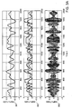
- FIG. 3 (a ) and 3(b) Sample waveforms for an adaptive ⁇ - ⁇ modulator implementing the adaptation algorithm described in Tab. 1 are shown in Figs. 3 (a ) and 3(b).
- the first trace 301 in Fig. 3(a) depicts an example of an input signal x(n).
- the second trace 302 in Fig. 3(a) shows the full wave rectified version
- the third trace 303 in Fig. 3(a) illustrates the full DAC-output signal z(n). In Fig.
- Traces 304, 305, and 306 represent an input signal x(n), the full wave rectified version
- and z(n) appears more pronounced, and the digital sequence c 0 (n) varies between 1 and 3.
- step size multiplier c(n) tracks the individual maxima and minima of input x(n).
- Signal c(n) can directly be used to estimate the instantaneous power of the input signal, which is advantageous, for example, in signal processing applications for automatic gain control (AGC) for speech signals.
- AGC automatic gain control
- Adaptive ⁇ - ⁇ modulation schemes typically use comparatively slow adaptation algorithms, where time constants in the range of tens of milliseconds are involved (usually referred to as "syllabic compression").
- SEC automatic gain control
- Adaptive ⁇ - ⁇ modulation schemes typically use comparatively slow adaptation algorithms, where time constants in the range of tens of milliseconds are involved (usually referred to as "syllabic compression").
- An example is Chakravarthy, C.
- Fig. 4 the SNR of various types of analog-to-digital converters are shown as a function of the input signal's power.
- Curve 402 is the SNR of an ideal standard sigma-delta modulator of 1st order with y a (n) ⁇ ⁇ 1. The maximum SNR is obtained at the maximum input power level, and a decrease of input power results in a decrease of the SNR. Comparing curves 401 and 402 clearly demonstrates the benefit of the adaptive-sigma delta modulator.
- Curve 402 is very similar to the segment of curve 401 having input levels smaller than about -50dB, shifted to the right by about 48dB. This shift reflects the additional 8 bits of signal z(n) as compared to y a (n).
- the adaptive sigma-delta modulator operates in a manner similar to a standard sigma-delta modulator, since the feedback-signal z(n) is a two-level signal, z(n) ⁇ ⁇ 1/256. Note that for high input levels, the SNR of the adaptive modulator is not substantially higher than for the standard modulator. However, the input dynamic range has been expanded by approximately 48dB.
- Curve 403 depicts the SNR of a sigma-delta-modulator of 2 nd order. Obviously, at lower input levels, the 2 nd order system is outperformed by the adaptive modulator. Curves 404 and 405 depict the SNR's of Pulse Code Modulation (PCM) systems with 13 and 14 bit resolutions, respectively. Whereas the 14-bit PCM system is superior to the adaptive sigma-delta modulator for all input levels, the 13-bit PCM system is inferior at least at low-level input signals.
- PCM Pulse Code Modulation
- the adaptive sigma-delta modulator includes a multi-bit DAC 204 in the feedback loop, as shown in Fig. 2 , since the feedback signal z(n) is a multi-level signal.
- the specifications of this DAC 204 is chosen to have minimal effects on the SNR of the adaptive sigma-delta modulator.
- this noise (multiplied by -1) is directly added to the input signal and enhances the noise energy in the base band.
- the DAC 204 the following assumptions can be made:
- the single weights can only be realized as 128 1 ⁇ ⁇ 128 , 16 1 ⁇ ⁇ 16 , 4 1 ⁇ ⁇ 4 , and 1 ⁇ ⁇ , which results in a deviation from the nominal value.
- the adaptive sigma-delta modulator shown in Fig. 2 yields its optimum performance if the input x(n) is a zero-mean signal, or if the dc-component of x(n) is at least close to zero. However, if x(n) contains a considerable dc-component, the input dynamic range is reduced.
- an input signal with a dc-component and comparatively very small ac-component The step size reduction will be governed by the de-component and not the ac-component, and thus it remains too large.
- Dc-components can be introduced from either the input signal directly, or by offset-errors due to non-ideal components of the modulator itself. In practical implementations, offset errors in the DAC might occur. In any case, a high-pass filter removes most problems involved with dc- or very low frequency components.
- an implementation of a high-pass filter is implemented as shown in Fig. 6 .
- the adaptive sigma-delta modulator 203 of Fig. 2 is embedded in a feedback loop system, which represents a typical digital high-pass filter.
- the digital output z 0 (n) of the modulator is first accumulated 601, resulting in signal az 0 (n), and then multiplied 602 by a factor ⁇ , resulting in signal w 0 (n).
- Digital-to-analog conversion of w 0 (n) by means of a second DAC 603 results in signal w(n), which is subtracted 604 from the input x(n).
- HP z 1 - z - 1 1 - 1 - ⁇ ⁇ z - 1 .
- a numeric version of a multibit sigma-delta modulator 701 into the system results, for example, in the system as shown in Fig. 7 .
- signal az 0 (n) comprises 19 bits.
- this signal is converted to output signal 1024w d0 (n), which represents the input signal az 0 (n), delayed by one clock period.
- two identical 9-bit numeric quantizers 702 and 703 with a transfer characteristics of mid-tread-type are employed. Possible output numbers are -255, -254, .., -2, -1, 0, 1, 2, ... 254, 255. Note that using the numeric multibit sigma-delta modulator provides a very efficient method to implement the constant-factor multiplication 1/1024.
- Signal w 0 (n) is the sigma-delta version of signal a ⁇ z 0 n 1024 .
- the number of bits has been reduced from 19 in signal az 0 (n) to 9 in signal w 0 (n).
- both signals contain almost the same information.
- Information contained in the 10 bit difference is preserved in the temporal fine structure of w 0 (n).
- both signals z 0 (n) and w 0 (n) are composed of 9 bits, the 2 DACs of Fig.
- Fig. 8 depicts typical waveforms of the system in Fig. 7 .
- the first trace 801 shows an input signal x(n) with a step-like transition after 2ms.
- the third trace 803 shows the difference signal x(n)-w(n), which represents the high-pass filtered version of x(n).
- Fig. 9 the SNR obtained with the system depicted in Fig. 7 , using an ideal high-pass filter, is compared with the SNR obtained with the system depicted in Fig. 8 , which uses a high-pass filter with numeric multibit sigma-delta modulator (employing 9-bit quantizers of mid-tread type), as waveforms 901 and 902, respectively.
- the same input signal as specified in Figs. 4 and 5 , with N 20000, is used.
- the noise power in the signal band is derived from the difference between the system output signal and a reference signal.
- the reference signal is the high-pass filtered version of x(n), assuming the ideal transfer function (3).
- the additional noise introduced by the numeric multibit sigma-delta modulator results in a loss of SNR at low input power levels.
- the input dynamic range is reduced by approximately 6dB.
- the decrease of SNR at high input levels is due to a clipping effect and appears, if the sum w 0 (n)+z 0 (n) exceeds the range [-255, 255].
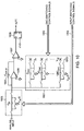
- the 9-bit DAC 1001 is composed of an array of 8 binary weighted capacitors C DAC , 2C DAC , 4C DAC , 8C DAC , 16C DAC , 32C DAC , 64C DAC , and 128C DAC .
- the analog input signal is processed by the input sampling stage 1003.
- Charge- and discharge operations of the arrays 1001 and 1003 are digitally controlled by DAC-Switching control signals 1002 and Input-Switching control signals 1004, which are generated in the digital part of the modulator.
- each ⁇ - ⁇ clock period is subdivided into two sections of roughly equal length, the "sampling-section" and the "accumulation-section”.
- all capacitors in 1001 and 1003 are disconnected from the operational amplifier.
- the switches at the capacitors are set such that a charge Q in (n) proportional to the input signal x(n) is stored to 1003, and a charge Q DAC (n) proportional to the (negative) overall feedback signal -[z(n)+w(n)] is stored to 1001 (cf. Fig.7 ).
- input signal x(n) and the overall feedback signal z(n)+w(n ) may be referred to a constant potential, such as V ref /2.
- V ref /2 a constant potential
- the ports of the capacitors in 1001 and 1003 are switched such that the capacitors are discharged and the sum of the charges Q in (n)+Q DAC (n) is forced to flow into the accumulation capacitor 1005.
- the charge in capacitor 1005 is changed by Q in (n)+Q DAC (n).
- the sign of the new potential at the output of the operational amplifier referred to V ref /2 is sensed by the comparator 1007, and clocked into flip-flop 1008 at the end of the "accumulation-section". Note that for proper operation both, chargeaccumulation and the sign-sensing have to be finished within the "accumulation-section", and therefore the response time of the comparator has to be shorter than 50% of a ⁇ - ⁇ clock period.
- the adaptive ⁇ - ⁇ modulator imposes harsh requirements on the comparator 1007.
- the enhanced input dynamic range causes an equally enhanced dynamic range of the signal at the output of amplifier 1006, which applies at the comparator input.
- the corresponding range for an adaptive modulator with a 9-bit DAC is +/-1V for the largest value of c(n), and +/-3.9mV for the smallest value of c(n).
- the switching behavior of the comparator has to be equal for both cases.
- comparators tend to become slower as the input signal differences get smaller, and signals in the +/-3.9mV range are adversely affected. Thus, it has to be ensured that the comparator is sufficiently fast to track very small input signals.
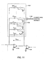
- Fig.11 one way to reduce the dynamic range of the comparator input signal is explained with the help of Fig.11 .
- the accumulation capacitor 1005 of Fig. 10 is replaced by an SC-array 1101 of capacitors C ACC , C ACC , 2C ACC , 4C ACC , 8C ACC , 16C ACC , 32C ACC , 64C ACC , and 128C ACC .
- the size of the feedback capacitor is adapted to the instantaneous input signal power.
- An overall feedback capacitance C ACC,TOT (n) is realized by switching a particular number of single capacitors in parallel. If the power of the input signal is small, the mean charge across the accumulation capacitor will also be comparatively small.
- Case (2) Removing capacitor 1105 from the active array C ACC,TOT is achieved by switching 1106 such that the second port is connected to the reference voltage V ref /2 during the whole period number (n+1). Since this potential is equal the virtual potential of the inverting input of amplifier 1103, the amplifier forces the output to change its potential from Q ACC n C ACC , TOT n to Q ACC n C ACC , TOT n - 2 ⁇ C ACC .
- Q ACC (n) is the charge in array 1105 at the end of the clock period number n and in the "sampling-section" of period number (n+1).
- the adaptation of C ACC,TOT (n) is achieved based, at least in part, on digital signal c 0 (n).
- An example of an adaptation scheme is summarized in Table 2 for an 8-bit signal c 0 (n).
- the first non-zero bit within c 0 (n) is directly used to define C ACC,TOT (n). Note that the exact value of C ACC,TOT (n) is not critically important.
- the adaptation algorithm ensures that (1) on average, the magnitude of voltage U ACC is maximized, but the instantaneous value of U ACC does not exceed specified limits at no time instant, and (2) the switching between different configurations of 1101 is performed without any significant loss of charge, and preferably no loss of charge. Loss of charge in 1101 results in accumulation errors and thus reduces the system performance.
- the above-described manner for reducing the dynamic range of the comparator input signal may be applicable to a wide variety of adaptive and non-adaptive ⁇ - ⁇ modulators, and is not limited to an adaptive ⁇ - ⁇ modulator in which the adaptation stage tends to keep the instantaneous magnitude of the analog feedback signal z(n) within the first range [-a, +a] and greater than the analog input signal's x(n) instantaneous magnitude.
- Alternative embodiments of the invention may be implemented as a computer program product for use with a computer system.
- Such implementation may include a series of computer instructions fixed either on a tangible medium, such as a computer readable media (e.g., a diskette, CD-ROM, ROM, or fixed disk), or fixed in a computer data signal embodied in a carrier wave that is transmittable to a computer system via a modem or other interface device, such as a communications adapter connected to a network over a medium.
- the medium may be either a tangible medium (e.g., optical or analog communications lines) or a medium implemented with wireless techniques (e.g., microwave, infrared or other transmission techniques).
- the series of computer instructions embodies all or part of the functionality previously described herein with respect to the system.
- Those skilled in the art should appreciate that such computer instructions can be written in a number of programming languages for use with many computer architectures or operating systems.
- such instructions may be stored in any memory device, such as semiconductor, magnetic, optical or other memory devices, and may be transmitted using any communications technology, such as optical, infrared, microwave, or other transmission technologies.
- It is expected that such a computer program product may be distributed as a removable medium with accompanying printed or electronic documentation (e.g., shrink wrapped software), preloaded with a computer system (e.g., on system ROM or fixed disk), or distributed from a server or electronic bulletin board over the network (e.g., the Internet or World Wide Web).
Claims (21)
- Adaptiver Sigma-Delta-Modulator (203), welcher aufweist: eine Eingangsstufe (208), welche ein Differenzsignal herstellt, welches die Differenz zwischen einem analogen Eingangssignal (x(n)) und einem analogen Rückkopplungssignal (z(n)) darstellt, wobei die Amplitude des analogen Eingangssignals (x(n)) innerhalb eines ersten Bereichs [-a, +a] liegt; eine Akkumulatorstufe (209), welche ein Komparator- bzw. Vergleichseingangssignal ausgibt, welches eine Funktion einer Akkumulation des Differenzsignals ist, wobei die Akkumulatorstufe (209) einen Akkumulationskondensator (1105) beinhaltet; eine Quantisierungsstufe (202), welche einen Komparator (1007) besitzt, welcher das Komparator-Eingangssignal von der Akkumulatorstufe (209) empfängt und ein quantisiertes Digitalsignal (y0(n)) herstellt, welches eine Quantisierung des Komparator-Eingangssignals darstellt; eine Adaptionsstufe (205), welche basierend auf dem quantisierten Digitalsignal (y0(n)) ein digitales Ausgangssignal (z0(n))liefert; und eine Digital/Analog-Wandlerstufe (204), welche das digitale Ausgangssignal (z0(n)) in das analoge Rückkopplungssignal (z(n)) wandelt; wobei der adaptive Sigma-Delta-Modulator (203) dadurch gekennzeichnet ist, dass der Akkumulationskondensator (1105) eine Kapazität besitzt, welche variabel gesteuert ist, um die Akkumulation des Differenzsignals in das Komparator-Eingangssignal umzuformen, um den dynamischen Bereich des Komparator-Eingangssignals zu reduzieren.
- Adaptiver Sigma-Delta-Modulator nach Anspruch 1, wobei die Adaptionsstufe (205) eine Vervielfacherstufe beinhaltet, welche das quantisierte Digitalsignal (y0(n)) mit einer Schrittweite (c0(n)) multipliziert, wobei die Schrittweite (c0(n)) so festgelegt ist, um die momentane Größe des analogen Rückkopplungssignals (z(n)) innerhalb des ersten Bereiches [-a, +a] und größer als die momentane Größe des analogen Eingangssignals (x(n)) zu treiben.
- Adaptiver Sigma-Delta-Modulator nach Anspruch 1, wobei das akkumulierte Signal wenigstens zum Teil auf der Spannung über den Akkumulationskondensator (1005) hinweg basiert.
- Adaptiver Sigma-Delta-Modulator nach Anspruch 1, wobei die Kapazität über den Akkumulationskondensator (1005) hinweg variabel so gesteuert wird, dass die durchschnittliche Größe der Spannung über den Akkumulationskondensator (1005) hinweg erhöht wird, während sichergestellt wird, dass die momentane Größe der Spannung über den Akkumulationskondensator (1005) hinweg nicht einen vorher festgelegten Wert überschreitet.
- Adaptiver Sigma-Delta-Modulator nach Anspruch 1, wobei der Akkumulationskondensator (1005) zwischen einem Eingang und einem Ausgang eines Operationsverstärkers (1006) gekoppelt ist.
- Adaptiver Sigma-Delta-Modulator nach Anspruch 1, wobei die Adaptionsstufe (205) eine Vervielfacherstufe beinhaltet, welche das quantisierte Digitalsignal (y0(n)) mit einer Schrittweite (c0(n)) multipliziert, und wobei die Kapazität über den Akkumulationskondensator (1005) basierend (wenigstens zum Teil) auf der Schrittweite (c0(n)) variabel gesteuert wird.
- Adaptiver Sigma-Delta-Modulator nach Anspruch 1, wobei der Akkumulationskondensator (1005) ein Feld von Kondensatoren (1101) beinhaltet, wobei jeder Kondensator in dem Feld (1101) in der Lage ist, so geschaltet zu werden, um die Kapazität über den Akkumulationskondensator (1005) hinweg zu variieren.
- Adaptiver Sigma-Delta-Modulator nach Anspruch 1, wobei der Digital/AnalogWandler (204) ein Feld von gewichteten Kondensatoren beinhaltet, wobei das Feld der gewichteten Kondensatoren in der Lage ist, eine Ladung (QDAC(n)) negativ proportional zu dem digitalen Ausgangssignal (z0(n)) zu erlangen.
- Adaptiver Sigma-Delta-Modulator nach Anspruch 1, wobei die Eingangs-Abtaststufe (1003) einen Eingangsabtastkondensator beinhaltet, wobei der Eingangsabtastkondensator in der Lage ist, eine Ladung (Qin(n)) proportional zu dem analogen Eingangssignal (x(n)) zu erlangen.
- Verfahren für das Adaptieren einer Sigma-Delta-Modulation, wobei das Verfahren aufweist: Herstellen eines Differenzsignals, welches die Differenz zwischen einem analogen Eingangssignal (x(n)) und einem adaptiven Rückkopplungssignal (z(n)) aufweist, wobei die Amplitude des analogen Eingangssignals (x(n)) innerhalb eines ersten Bereiches [-a, +a] liegt; Herstellen eines Komparator-Eingangssignals, welches eine Funktion einer Akkumulierung in einem Akkumulationskondensator (1105) des Differenzsignals ist; Empfangen des Komparator-Eingangssignals an einem Komparator (1007) und Herstellen eines quantisierten digitalen Signals (y0(n)), welches eine Quantisierung des Komparator-Eingangssignals darstellt; Herstellen eines digitalen Ausgangssignals (z0(n)), basierend auf dem quantisierten Digitalsignal (y0(n)); und Ausführen einer Digital/Analog-Wandlung an dem digitalen Ausgangssignal (z0(n)), um das adaptive Rückkopplungssignal (z0(n)) herzustellen; wobei das Verfahren dadurch gekennzeichnet ist, dass das Herstellen des Komparator-Eingangssignals das variable Steuern der Kapazität über den Akkumlationskondensator (1005) hinweg beinhaltet, um die Akkumulation des Differenzsignals in das Komparator-Eingangssignal so überzuführen, um den dynamischen Bereich des Komparator-Eingangssignals zu reduzieren.
- Verfahren nach Anspruch 10, wobei das Herstellen eines digitalen Ausgangssignals (z0(n)) das Multiplizieren des quantisierten Digitalsignals (y0(n)) mit einer Schrittweite (c0(n)) beinhaltet, wobei die Schrittweite (c0(n)) so festgelegt ist, um die momentane Größe des analogen Rückkopplungssignals (z(n) innerhalb des ersten Bereiches [-a, +a] und größer als die momentane Größe des analogen Eingangssignals (x(n)) zu treiben.
- Verfahren nach Anspruch 10, wobei das Herstellen des akkumulierten Signals das Speichern der Ladung über den Akkumulationskondensator hinweg beinhaltet, wobei die Ladung die Akkumulation bzw. Addierung des Differenzsignals darstellt.
- Verfahren nach Anspruch 10, wobei das variable Steuern der Kapazität über den Akkumulationskondensator hinweg das variable Steuern der Kapazität über den Akkumulationskondensator so beinhaltet, um die durchschnittliche Spannung über den Akkumulationskondensator hinweg zu erhöhen, während sichergestellt wird, dass die momentane Spannung über den Akkumulationskondensator hinweg nicht einen vorher festgelegten Wert übersteigt.
- Verfahren nach Anspruch 10, wobei das Herstellen des digitalen Ausgangssignals (z0(n)) das Multiplizieren des quantisierten Digitalsignals (y0(n)) und einer Schrittweite (c0(n)) beinhaltet und wobei das variable Steuern der Kapazität über den Akkumulationskondensator hinweg das Variieren der Kapazität über den Akkumulationskondensator hinweg basierend auf, wenigstens zum Teil, auf der Schrittweite (c0(n)) beinhaltet.
- Verfahren nach Anspruch 10, wobei der Akkumulationskondensator zwischen einem Eingang und einem Ausgang eines Operationsverstärkers gekoppelt ist.
- Verfahren nach Anspruch 10, wobei der Akkumulationskondensator ein Feld von Kondensatoren beinhaltet und wobei das variable Steuern der Kapazität über den Akkumlationskondensator hinweg das Schalten wenigstens eines Kondensators in dem Array so beinhaltet, dass die Kapazität über den Akkumulationskondensator hinweg variiert wird.
- Verfahren nach Anspruch 16, wobei das Schalten wenigstens eines Kondensators in dem Feld das Trennen wenigstens eines Kondensators in dem Feld so beinhaltet, um die Kapazität über den Akkumulationskondensator hinweg zu erniedrigen.
- Verfahren nach Anspruch 16, wobei das Schalten wenigstens eines Kondensators in dem Feld das Aktivieren wenigstens eines Kondensators in dem Feld so beinhaltet, um die Kapazität über den Akkumlationskondensator hinweg zu erhöhen.
- Verfahren nach Anspruch 10, wobei das variable Steuern der Kapazität über den Akkumulationskondensator hinweg das Verlieren von hauptsächlich keiner Ladung über den Akkumulationskondensator hinweg beinhaltet.
- Verfahren nach Anspruch 10, wobei das Durchführen der Digital/Analog-Wandlung an dem digitalen Ausgangssignal (z0(n)), um das adaptive Rückkopplungssignal (z(n)) herzustellen, das Erwerben einer Ladung (QDAC(n)) auf einem Feld von gewichteten Kondensatoren beinhaltet, wobei die Ladung (QDAC(n)) negativ proportional zu dem digitalen Ausgangssignal (z0(n)) ist.
- Verfahren nach Anspruch 10, wobei das Herstellen des Differenzsignals das Erwerben einer Ladung (Qin(n)) an einem Eingangsabtastkondensator beinhaltet, wobei die Ladung (Qin(n)) proportional zu dem analogen Eingangssignal (x(n)) ist.
Priority Applications (1)
| Application Number | Priority Date | Filing Date | Title |
|---|---|---|---|
| DE60333957T DE60333957D1 (de) | 2003-09-26 | 2003-09-26 | Akkumulator für adaptive Sigma-Delta-Modulation |
Applications Claiming Priority (2)
| Application Number | Priority Date | Filing Date | Title |
|---|---|---|---|
| EP03758484A EP1665544B1 (de) | 2003-09-26 | 2003-09-26 | Akkumulator für adaptive sigma-delta modulation |
| PCT/IB2003/004846 WO2005031980A1 (en) | 2003-09-26 | 2003-09-26 | Accumulator for adaptive sigma-delta modulation |
Related Parent Applications (2)
| Application Number | Title | Priority Date | Filing Date |
|---|---|---|---|
| EP03758484.4 Division | 2003-09-26 | ||
| EP03758484A Division EP1665544B1 (de) | 2003-09-26 | 2003-09-26 | Akkumulator für adaptive sigma-delta modulation |
Publications (2)
| Publication Number | Publication Date |
|---|---|
| EP1855384A1 EP1855384A1 (de) | 2007-11-14 |
| EP1855384B1 true EP1855384B1 (de) | 2010-08-25 |
Family
ID=34385740
Family Applications (2)
| Application Number | Title | Priority Date | Filing Date |
|---|---|---|---|
| EP07075367A Expired - Lifetime EP1855384B1 (de) | 2003-09-26 | 2003-09-26 | Akkumulator für adaptive Sigma-Delta-Modulation |
| EP03758484A Expired - Lifetime EP1665544B1 (de) | 2003-09-26 | 2003-09-26 | Akkumulator für adaptive sigma-delta modulation |
Family Applications After (1)
| Application Number | Title | Priority Date | Filing Date |
|---|---|---|---|
| EP03758484A Expired - Lifetime EP1665544B1 (de) | 2003-09-26 | 2003-09-26 | Akkumulator für adaptive sigma-delta modulation |
Country Status (7)
| Country | Link |
|---|---|
| EP (2) | EP1855384B1 (de) |
| JP (1) | JP4555776B2 (de) |
| AT (2) | ATE479232T1 (de) |
| AU (1) | AU2003274509B2 (de) |
| CA (1) | CA2540146C (de) |
| DE (2) | DE60333957D1 (de) |
| WO (1) | WO2005031980A1 (de) |
Families Citing this family (3)
| Publication number | Priority date | Publication date | Assignee | Title |
|---|---|---|---|---|
| US9310953B1 (en) | 2014-11-25 | 2016-04-12 | Cypress Semiconductor Corporation | Full-wave synchronous rectification for self-capacitance sensing |
| JP6753330B2 (ja) * | 2017-02-15 | 2020-09-09 | 株式会社デンソー | Δς変調器、δσa/d変換器およびインクリメンタルδσa/d変換器 |
| US10284222B1 (en) * | 2018-02-09 | 2019-05-07 | Texas Instruments Incorporated | Delta-sigma converter with pre-charging based on quantizer output code |
Family Cites Families (7)
| Publication number | Priority date | Publication date | Assignee | Title |
|---|---|---|---|---|
| US4860012A (en) * | 1986-02-14 | 1989-08-22 | Microchip Technology Incorporated | Integrated analog-to-digital converter |
| JP3048263B2 (ja) * | 1991-09-02 | 2000-06-05 | 株式会社日立製作所 | アナログ/ディジタル変換器 |
| US6535153B1 (en) * | 1999-02-04 | 2003-03-18 | Med-El Electromedizinische Gerate Ges.M.B.H. | Adaptive sigma-delta modulation with one-bit quantization |
| US6885326B2 (en) * | 1999-02-04 | 2005-04-26 | Med-El Elektromedizinische Geraeta Gmbh | Accumulator for adaptive Σ-Δ modulation |
| WO2002009292A2 (en) * | 2000-07-13 | 2002-01-31 | The Regents Of The University Of California | Adaptive sigma-delta modulation with improved dynamic range |
| US20020146865A1 (en) * | 2001-04-04 | 2002-10-10 | Hoel Jeffrey H. | Method for selecting from standardized set of integrated circuit mask features |
| WO2003084074A1 (en) * | 2002-03-28 | 2003-10-09 | Med-El Elektromedizinische Geräte G.M.B.H. | A system and method for adaptive sigma-delta modulation |
-
2003
- 2003-09-26 DE DE60333957T patent/DE60333957D1/de not_active Expired - Lifetime
- 2003-09-26 WO PCT/IB2003/004846 patent/WO2005031980A1/en active Application Filing
- 2003-09-26 EP EP07075367A patent/EP1855384B1/de not_active Expired - Lifetime
- 2003-09-26 AT AT07075367T patent/ATE479232T1/de active
- 2003-09-26 JP JP2005509157A patent/JP4555776B2/ja not_active Expired - Lifetime
- 2003-09-26 DE DE60324610T patent/DE60324610D1/de not_active Expired - Lifetime
- 2003-09-26 AT AT03758484T patent/ATE413732T1/de active
- 2003-09-26 EP EP03758484A patent/EP1665544B1/de not_active Expired - Lifetime
- 2003-09-26 CA CA2540146A patent/CA2540146C/en not_active Expired - Lifetime
- 2003-09-26 AU AU2003274509A patent/AU2003274509B2/en not_active Expired
Also Published As
| Publication number | Publication date |
|---|---|
| JP4555776B2 (ja) | 2010-10-06 |
| AU2003274509A1 (en) | 2005-04-14 |
| EP1665544A1 (de) | 2006-06-07 |
| DE60333957D1 (de) | 2010-10-07 |
| ATE479232T1 (de) | 2010-09-15 |
| DE60324610D1 (de) | 2008-12-18 |
| CA2540146A1 (en) | 2005-04-07 |
| EP1665544B1 (de) | 2008-11-05 |
| ATE413732T1 (de) | 2008-11-15 |
| CA2540146C (en) | 2012-11-13 |
| JP2007516626A (ja) | 2007-06-21 |
| WO2005031980A1 (en) | 2005-04-07 |
| EP1855384A1 (de) | 2007-11-14 |
| AU2003274509B2 (en) | 2008-12-18 |
Similar Documents
| Publication | Publication Date | Title |
|---|---|---|
| US7339510B2 (en) | Accumulator for adaptive sigma-delta modulation | |
| EP1488525B1 (de) | System und verfahren für adaptive sigma-delta modulation | |
| US6727833B2 (en) | Adaptive ΣΔ modulation with one-bit quantization | |
| US5243345A (en) | Sigma-delta modulator having a plural order loop filter with successive filter sections of successively smaller signal excursion range | |
| JP5154659B2 (ja) | フィードバックパスにおいてビット数の減少したマルチビットシグマ・デルタ変調器 | |
| EP0756384A2 (de) | Verfahren zur Erhöhung der Stabilität eines Sigma-Delta-Modulators unter Verwendung eines Zittersignals | |
| US20080272946A1 (en) | Signal processing system using delta-sigma modulation having an internal stabilizer path with direct output-to-integrator connection | |
| US7453382B2 (en) | Method and apparatus for A/D conversion | |
| WO1998011668A1 (en) | Wide dynamic range a/d converter | |
| WO2005122409A1 (en) | Analog-to-digital modulation | |
| JP2004248288A (ja) | 適応シグマ−デルタ変調器およびシグマ−デルタ変調を実施する方法 | |
| EP1855384B1 (de) | Akkumulator für adaptive Sigma-Delta-Modulation | |
| JP3040546B2 (ja) | ノイズシェーピングa−d変換器 | |
| JPH09307447A (ja) | 高次δς変調器とδς変調型コンバータ | |
| CN112953533B (zh) | 一种改进型低失真Sigma-Delta调制器 | |
| Zierhofer | Adaptive Delta-Sigma Modulation for Enhanced Input Dynamic Range | |
| Chen et al. | An adaptive sigma-delta modulator with improved dynamic range |
Legal Events
| Date | Code | Title | Description |
|---|---|---|---|
| PUAI | Public reference made under article 153(3) epc to a published international application that has entered the european phase |
Free format text: ORIGINAL CODE: 0009012 |
|
| 17P | Request for examination filed |
Effective date: 20070607 |
|
| AC | Divisional application: reference to earlier application |
Ref document number: 1665544 Country of ref document: EP Kind code of ref document: P |
|
| AK | Designated contracting states |
Kind code of ref document: A1 Designated state(s): AT BE BG CH CY CZ DE DK EE ES FI FR GB GR HU IE IT LI LU MC NL PT RO SE SI SK TR |
|
| 17Q | First examination report despatched |
Effective date: 20080609 |
|
| AKX | Designation fees paid |
Designated state(s): AT BE BG CH CY CZ DE DK EE ES FI FR GB GR HU IE IT LI LU MC NL PT RO SE SI SK TR |
|
| GRAP | Despatch of communication of intention to grant a patent |
Free format text: ORIGINAL CODE: EPIDOSNIGR1 |
|
| GRAS | Grant fee paid |
Free format text: ORIGINAL CODE: EPIDOSNIGR3 |
|
| GRAA | (expected) grant |
Free format text: ORIGINAL CODE: 0009210 |
|
| AC | Divisional application: reference to earlier application |
Ref document number: 1665544 Country of ref document: EP Kind code of ref document: P |
|
| AK | Designated contracting states |
Kind code of ref document: B1 Designated state(s): AT BE BG CH CY CZ DE DK EE ES FI FR GB GR HU IE IT LI LU MC NL PT RO SE SI SK TR |
|
| REG | Reference to a national code |
Ref country code: GB Ref legal event code: FG4D |
|
| REG | Reference to a national code |
Ref country code: CH Ref legal event code: EP |
|
| REG | Reference to a national code |
Ref country code: IE Ref legal event code: FG4D |
|
| REF | Corresponds to: |
Ref document number: 60333957 Country of ref document: DE Date of ref document: 20101007 Kind code of ref document: P |
|
| REG | Reference to a national code |
Ref country code: NL Ref legal event code: VDEP Effective date: 20100825 |
|
| PG25 | Lapsed in a contracting state [announced via postgrant information from national office to epo] |
Ref country code: FI Free format text: LAPSE BECAUSE OF FAILURE TO SUBMIT A TRANSLATION OF THE DESCRIPTION OR TO PAY THE FEE WITHIN THE PRESCRIBED TIME-LIMIT Effective date: 20100825 |
|
| PGFP | Annual fee paid to national office [announced via postgrant information from national office to epo] |
Ref country code: AT Payment date: 20101119 Year of fee payment: 8 |
|
| PG25 | Lapsed in a contracting state [announced via postgrant information from national office to epo] |
Ref country code: CY Free format text: LAPSE BECAUSE OF FAILURE TO SUBMIT A TRANSLATION OF THE DESCRIPTION OR TO PAY THE FEE WITHIN THE PRESCRIBED TIME-LIMIT Effective date: 20100825 Ref country code: BG Free format text: LAPSE BECAUSE OF FAILURE TO SUBMIT A TRANSLATION OF THE DESCRIPTION OR TO PAY THE FEE WITHIN THE PRESCRIBED TIME-LIMIT Effective date: 20101125 Ref country code: PT Free format text: LAPSE BECAUSE OF FAILURE TO SUBMIT A TRANSLATION OF THE DESCRIPTION OR TO PAY THE FEE WITHIN THE PRESCRIBED TIME-LIMIT Effective date: 20101227 Ref country code: SI Free format text: LAPSE BECAUSE OF FAILURE TO SUBMIT A TRANSLATION OF THE DESCRIPTION OR TO PAY THE FEE WITHIN THE PRESCRIBED TIME-LIMIT Effective date: 20100825 |
|
| PG25 | Lapsed in a contracting state [announced via postgrant information from national office to epo] |
Ref country code: GR Free format text: LAPSE BECAUSE OF FAILURE TO SUBMIT A TRANSLATION OF THE DESCRIPTION OR TO PAY THE FEE WITHIN THE PRESCRIBED TIME-LIMIT Effective date: 20101126 Ref country code: BE Free format text: LAPSE BECAUSE OF FAILURE TO SUBMIT A TRANSLATION OF THE DESCRIPTION OR TO PAY THE FEE WITHIN THE PRESCRIBED TIME-LIMIT Effective date: 20100825 Ref country code: SE Free format text: LAPSE BECAUSE OF FAILURE TO SUBMIT A TRANSLATION OF THE DESCRIPTION OR TO PAY THE FEE WITHIN THE PRESCRIBED TIME-LIMIT Effective date: 20100825 Ref country code: NL Free format text: LAPSE BECAUSE OF FAILURE TO SUBMIT A TRANSLATION OF THE DESCRIPTION OR TO PAY THE FEE WITHIN THE PRESCRIBED TIME-LIMIT Effective date: 20100825 |
|
| PG25 | Lapsed in a contracting state [announced via postgrant information from national office to epo] |
Ref country code: MC Free format text: LAPSE BECAUSE OF NON-PAYMENT OF DUE FEES Effective date: 20100930 Ref country code: DK Free format text: LAPSE BECAUSE OF FAILURE TO SUBMIT A TRANSLATION OF THE DESCRIPTION OR TO PAY THE FEE WITHIN THE PRESCRIBED TIME-LIMIT Effective date: 20100825 |
|
| REG | Reference to a national code |
Ref country code: CH Ref legal event code: PL |
|
| PG25 | Lapsed in a contracting state [announced via postgrant information from national office to epo] |
Ref country code: SK Free format text: LAPSE BECAUSE OF FAILURE TO SUBMIT A TRANSLATION OF THE DESCRIPTION OR TO PAY THE FEE WITHIN THE PRESCRIBED TIME-LIMIT Effective date: 20100825 Ref country code: IT Free format text: LAPSE BECAUSE OF FAILURE TO SUBMIT A TRANSLATION OF THE DESCRIPTION OR TO PAY THE FEE WITHIN THE PRESCRIBED TIME-LIMIT Effective date: 20100825 Ref country code: RO Free format text: LAPSE BECAUSE OF FAILURE TO SUBMIT A TRANSLATION OF THE DESCRIPTION OR TO PAY THE FEE WITHIN THE PRESCRIBED TIME-LIMIT Effective date: 20100825 Ref country code: CZ Free format text: LAPSE BECAUSE OF FAILURE TO SUBMIT A TRANSLATION OF THE DESCRIPTION OR TO PAY THE FEE WITHIN THE PRESCRIBED TIME-LIMIT Effective date: 20100825 Ref country code: EE Free format text: LAPSE BECAUSE OF FAILURE TO SUBMIT A TRANSLATION OF THE DESCRIPTION OR TO PAY THE FEE WITHIN THE PRESCRIBED TIME-LIMIT Effective date: 20100825 |
|
| PG25 | Lapsed in a contracting state [announced via postgrant information from national office to epo] |
Ref country code: ES Free format text: LAPSE BECAUSE OF FAILURE TO SUBMIT A TRANSLATION OF THE DESCRIPTION OR TO PAY THE FEE WITHIN THE PRESCRIBED TIME-LIMIT Effective date: 20101206 |
|
| PLBE | No opposition filed within time limit |
Free format text: ORIGINAL CODE: 0009261 |
|
| STAA | Information on the status of an ep patent application or granted ep patent |
Free format text: STATUS: NO OPPOSITION FILED WITHIN TIME LIMIT |
|
| GBPC | Gb: european patent ceased through non-payment of renewal fee |
Effective date: 20101125 |
|
| PG25 | Lapsed in a contracting state [announced via postgrant information from national office to epo] |
Ref country code: IE Free format text: LAPSE BECAUSE OF NON-PAYMENT OF DUE FEES Effective date: 20100926 Ref country code: CH Free format text: LAPSE BECAUSE OF NON-PAYMENT OF DUE FEES Effective date: 20100930 Ref country code: LI Free format text: LAPSE BECAUSE OF NON-PAYMENT OF DUE FEES Effective date: 20100930 |
|
| 26N | No opposition filed |
Effective date: 20110526 |
|
| REG | Reference to a national code |
Ref country code: DE Ref legal event code: R097 Ref document number: 60333957 Country of ref document: DE Effective date: 20110526 |
|
| PG25 | Lapsed in a contracting state [announced via postgrant information from national office to epo] |
Ref country code: GB Free format text: LAPSE BECAUSE OF NON-PAYMENT OF DUE FEES Effective date: 20101125 |
|
| PG25 | Lapsed in a contracting state [announced via postgrant information from national office to epo] |
Ref country code: HU Free format text: LAPSE BECAUSE OF FAILURE TO SUBMIT A TRANSLATION OF THE DESCRIPTION OR TO PAY THE FEE WITHIN THE PRESCRIBED TIME-LIMIT Effective date: 20110226 Ref country code: LU Free format text: LAPSE BECAUSE OF NON-PAYMENT OF DUE FEES Effective date: 20100926 |
|
| PG25 | Lapsed in a contracting state [announced via postgrant information from national office to epo] |
Ref country code: TR Free format text: LAPSE BECAUSE OF FAILURE TO SUBMIT A TRANSLATION OF THE DESCRIPTION OR TO PAY THE FEE WITHIN THE PRESCRIBED TIME-LIMIT Effective date: 20100825 |
|
| REG | Reference to a national code |
Ref country code: AT Ref legal event code: MM01 Ref document number: 479232 Country of ref document: AT Kind code of ref document: T Effective date: 20120926 |
|
| PG25 | Lapsed in a contracting state [announced via postgrant information from national office to epo] |
Ref country code: AT Free format text: LAPSE BECAUSE OF NON-PAYMENT OF DUE FEES Effective date: 20120926 |
|
| REG | Reference to a national code |
Ref country code: FR Ref legal event code: PLFP Year of fee payment: 13 |
|
| REG | Reference to a national code |
Ref country code: FR Ref legal event code: PLFP Year of fee payment: 14 |
|
| REG | Reference to a national code |
Ref country code: FR Ref legal event code: PLFP Year of fee payment: 15 |
|
| REG | Reference to a national code |
Ref country code: FR Ref legal event code: PLFP Year of fee payment: 16 |
|
| PGFP | Annual fee paid to national office [announced via postgrant information from national office to epo] |
Ref country code: DE Payment date: 20220927 Year of fee payment: 20 |
|
| PGFP | Annual fee paid to national office [announced via postgrant information from national office to epo] |
Ref country code: FR Payment date: 20220926 Year of fee payment: 20 |
|
| REG | Reference to a national code |
Ref country code: DE Ref legal event code: R071 Ref document number: 60333957 Country of ref document: DE |