EP1850384B1 - Impedanz-angepasstes Photodetektormodul - Google Patents
Impedanz-angepasstes Photodetektormodul Download PDFInfo
- Publication number
- EP1850384B1 EP1850384B1 EP07002771.9A EP07002771A EP1850384B1 EP 1850384 B1 EP1850384 B1 EP 1850384B1 EP 07002771 A EP07002771 A EP 07002771A EP 1850384 B1 EP1850384 B1 EP 1850384B1
- Authority
- EP
- European Patent Office
- Prior art keywords
- substrate
- photodetector
- amplifier
- impedance
- tia
- Prior art date
- Legal status (The legal status is an assumption and is not a legal conclusion. Google has not performed a legal analysis and makes no representation as to the accuracy of the status listed.)
- Active
Links
Images


Classifications
-
- H—ELECTRICITY
- H10—SEMICONDUCTOR DEVICES; ELECTRIC SOLID-STATE DEVICES NOT OTHERWISE PROVIDED FOR
- H10W—GENERIC PACKAGES, INTERCONNECTIONS, CONNECTORS OR OTHER CONSTRUCTIONAL DETAILS OF DEVICES COVERED BY CLASS H10
- H10W90/00—Package configurations
-
- H—ELECTRICITY
- H05—ELECTRIC TECHNIQUES NOT OTHERWISE PROVIDED FOR
- H05K—PRINTED CIRCUITS; CASINGS OR CONSTRUCTIONAL DETAILS OF ELECTRIC APPARATUS; MANUFACTURE OF ASSEMBLAGES OF ELECTRICAL COMPONENTS
- H05K1/00—Printed circuits
- H05K1/02—Details
- H05K1/0213—Electrical arrangements not otherwise provided for
- H05K1/0237—High frequency adaptations
- H05K1/0243—Printed circuits associated with mounted high frequency components
-
- H—ELECTRICITY
- H05—ELECTRIC TECHNIQUES NOT OTHERWISE PROVIDED FOR
- H05K—PRINTED CIRCUITS; CASINGS OR CONSTRUCTIONAL DETAILS OF ELECTRIC APPARATUS; MANUFACTURE OF ASSEMBLAGES OF ELECTRICAL COMPONENTS
- H05K1/00—Printed circuits
- H05K1/18—Printed circuits structurally associated with non-printed electric components
- H05K1/189—Printed circuits structurally associated with non-printed electric components characterised by the use of flexible or folded printed circuits
-
- H—ELECTRICITY
- H05—ELECTRIC TECHNIQUES NOT OTHERWISE PROVIDED FOR
- H05K—PRINTED CIRCUITS; CASINGS OR CONSTRUCTIONAL DETAILS OF ELECTRIC APPARATUS; MANUFACTURE OF ASSEMBLAGES OF ELECTRICAL COMPONENTS
- H05K2201/00—Indexing scheme relating to printed circuits covered by H05K1/00
- H05K2201/01—Dielectrics
- H05K2201/0183—Dielectric layers
- H05K2201/0191—Dielectric layers wherein the thickness of the dielectric plays an important role
-
- H—ELECTRICITY
- H05—ELECTRIC TECHNIQUES NOT OTHERWISE PROVIDED FOR
- H05K—PRINTED CIRCUITS; CASINGS OR CONSTRUCTIONAL DETAILS OF ELECTRIC APPARATUS; MANUFACTURE OF ASSEMBLAGES OF ELECTRICAL COMPONENTS
- H05K2201/00—Indexing scheme relating to printed circuits covered by H05K1/00
- H05K2201/07—Electric details
- H05K2201/0776—Resistance and impedance
- H05K2201/0792—Means against parasitic impedance; Means against eddy currents
-
- H—ELECTRICITY
- H05—ELECTRIC TECHNIQUES NOT OTHERWISE PROVIDED FOR
- H05K—PRINTED CIRCUITS; CASINGS OR CONSTRUCTIONAL DETAILS OF ELECTRIC APPARATUS; MANUFACTURE OF ASSEMBLAGES OF ELECTRICAL COMPONENTS
- H05K2201/00—Indexing scheme relating to printed circuits covered by H05K1/00
- H05K2201/10—Details of components or other objects attached to or integrated in a printed circuit board
- H05K2201/10007—Types of components
- H05K2201/10121—Optical component, e.g. opto-electronic component
-
- H—ELECTRICITY
- H05—ELECTRIC TECHNIQUES NOT OTHERWISE PROVIDED FOR
- H05K—PRINTED CIRCUITS; CASINGS OR CONSTRUCTIONAL DETAILS OF ELECTRIC APPARATUS; MANUFACTURE OF ASSEMBLAGES OF ELECTRICAL COMPONENTS
- H05K2201/00—Indexing scheme relating to printed circuits covered by H05K1/00
- H05K2201/10—Details of components or other objects attached to or integrated in a printed circuit board
- H05K2201/10227—Other objects, e.g. metallic pieces
- H05K2201/10424—Frame holders
-
- H—ELECTRICITY
- H05—ELECTRIC TECHNIQUES NOT OTHERWISE PROVIDED FOR
- H05K—PRINTED CIRCUITS; CASINGS OR CONSTRUCTIONAL DETAILS OF ELECTRIC APPARATUS; MANUFACTURE OF ASSEMBLAGES OF ELECTRICAL COMPONENTS
- H05K2201/00—Indexing scheme relating to printed circuits covered by H05K1/00
- H05K2201/20—Details of printed circuits not provided for in H05K2201/01 - H05K2201/10
- H05K2201/2036—Permanent spacer or stand-off in a printed circuit or printed circuit assembly
-
- H—ELECTRICITY
- H05—ELECTRIC TECHNIQUES NOT OTHERWISE PROVIDED FOR
- H05K—PRINTED CIRCUITS; CASINGS OR CONSTRUCTIONAL DETAILS OF ELECTRIC APPARATUS; MANUFACTURE OF ASSEMBLAGES OF ELECTRICAL COMPONENTS
- H05K3/00—Apparatus or processes for manufacturing printed circuits
- H05K3/30—Assembling printed circuits with electric components, e.g. with resistors
- H05K3/306—Assembling printed circuits with electric components, e.g. with resistors with lead-in-hole components
-
- H—ELECTRICITY
- H10—SEMICONDUCTOR DEVICES; ELECTRIC SOLID-STATE DEVICES NOT OTHERWISE PROVIDED FOR
- H10W—GENERIC PACKAGES, INTERCONNECTIONS, CONNECTORS OR OTHER CONSTRUCTIONAL DETAILS OF DEVICES COVERED BY CLASS H10
- H10W90/00—Package configurations
- H10W90/701—Package configurations characterised by the relative positions of pads or connectors relative to package parts
- H10W90/751—Package configurations characterised by the relative positions of pads or connectors relative to package parts of bond wires
- H10W90/753—Package configurations characterised by the relative positions of pads or connectors relative to package parts of bond wires between laterally-adjacent chips
Definitions
- the present invention relates to a photodetector module that is equipped with a photodetector and is connected to a substrate to which an electronic signal generated by photoelectrical conversion in the photodetector is transferred.
- Patent Document 1 Japanese Unexamined Patent Application, Laid-Open No. H11-238916
- the Patent Document 1 proposes to remove the inductance component by placing a metal sleeve on the periphery of the lead pin to form a coaxial line consisting of the lead pin and the metal sleeve.
- the prior art also comprises document US 2005/0175312 A1 that describes an optical transmitter.
- Patent Document 1 Although many conventional techniques including the above-mentioned Patent Document 1 consider impedance matching, those techniques do not basically consider power saving for a photodetector module. However, users of photodetector modules require that the photodetector modules have matched impedance and in addition consume a low amount of power.
- An object of the present invention is to provide a photodetector module that has matched impedance and has low power consumption, in order to respond to the above requirements.
- the photodetector module of the present invention is provided with a photodetector and is connected to a substrate that is a target of transmission of an electric signal which is photoelectrically converted in the photodetector, the photodetector module comprising: an amplifier for amplifying the electric signal received from the photodetector; a board on which the photodetector and the amplifier are mounted; a dielectric placed between the board and the substrate; and a lead pin extending through the board and the dielectric to the substrate, so as to transfer the electric signal amplified by the amplifier to the substrate; wherein output of the amplifier includes a capacitance component, and an output impedance of the amplifier is higher than an impedance that matches with the substrate; and thickness of the dielectric in a direction from the board to the substrate is such that an inductance component of the lead pin includes an inductance component canceling the capacitance component of the amplifier, and impedance matching with the substrate can be achieved.
- the present invention employs an amplifier of high impedance, whose output includes a capacitance component, in order to achieve power saving in the amplifier. Owing to the high output impedance of the amplifier, impedance matching with the substrate is lost. To solve this problem, the present invention provides a dielectric to cancel the capacitance component of the output of the amplifier and to achieve impedance matching.
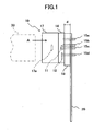
- the photodetector module of the present embodiment is connected to a flexible substrate 20.
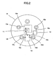
- This photodetector module 10 comprises: a photodetector 11 that converts an optical signal from an optical fiber 30 into an electric signal; a transimpedance amplifier (hereinafter, referred to as TIA) 12 that amplifies the electric signal received from the photodetector 11; a filter 13; a metallic stem 14 on which the mentioned components are mounted; a metallic cap 17 on which an optical system 17a for condensing light from the optical fiber 30 is mounted; a dielectric plate 18 that is placed between the stem 14 and the flexible substrate 20; and a plurality of lead pins 15a, 15b, 15c and 15d that extend to the substrate 20 through the stem 14 and the dielectric plate 18 in order to electrically connect the respective elements mounted on the stem 14 to the substrate 20.
- TIA transimpedance amplifier
- the TIA 12 performs impedance transformation of the electric current signal received from the photodetector 11, amplifies the electric signal, and outputs the amplified signal as a voltage signal.
- the plurality of lead pins 15a, 15b, 15c and 15d includes a power supply pin 15a for supplying power from the substrate 20 to the photodetector 11, a power supply pin 15b for supplying power from the substrate 20 to the TIA 12, and signal transfer pins 15c and 15d for transferring electric signals from TIA 12 to the substrate 20.
- the power supply pin 15a for the photodetector 11 is connected to the photodetector 11 through a power supply wire 16a.
- the power supply pin 15b for the TIA 12 is connected to the filter 13 through a power supply wire 16b, and the filter 13 to TIA 12 through power supply wires 16e.
- the photodetector 11 and TIA 12 are connected with each other through a signal transfer wire 16f.
- TIA 12 is connected to the signal transfer pins 15c and 15d through signal transfer wires 16c and 16d, respectively.
- the substrate 20 has a characteristic impedance of 50 ⁇ . Accordingly, when the output impedance of TIA 12 is 50 ⁇ , the impedance of the photodetector module 10 is matched with the substrate 20.
- Fig. 4 is a Smith chart that shows the complex reflection coefficient, in other words, the scattering coefficient s of a signal viewed from the signal transfer pin 15d toward the input port (i.e. the photosensitive part) of the photodetector 11, changing the frequency from 0 Hz through 5 GHz, assuming that the dielectric plate 18 is not provided.
- the horizontal axis is a real axis and the vertical axis is an imaginary axis.
- the output impedance of TIA 12 is 80 ⁇ at 0 Hz, and, as the frequency becomes higher, the scattering coefficient s swings to the -j side and the capacitance component increases.
- the output of the TIA 12 includes the capacitance component, and that the output impedance of the TIA 12 is 80 ⁇ , which is higher than an impedance (50 ⁇ ) that matches with the substrate 20.
- the output impedance of the TIA 12 is raised, and accordingly power consumption of the TIA 12 can be reduced.
- the dielectric plate 18 is arranged between the stem 14 and the flexible substrate 20, so that the inductance component that has inductivity, i.e. the +j component, is generated to cancel the capacitance component of the output of the TIA 12, in order to achieve impedance matching with the substrate 20.
- the thickness of the dielectric plate 18, namely, the distance d between the stem 14 and the substrate 20, is adjusted to obtain an inductance component that can cancel the capacitance component of the output of the TIA 12.
- Flame Retardant type 4 (FR4) is used for the dielectric plate 18.
- This FR4 is a flame retardant print board material, which is a composite material of glass and epoxy resin and has a dielectric constant ⁇ of 4.8.
- the present invention is not limited to this material.
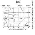
- the distance d between the stem 14 and the substrate 20 is determined by electromagnetic field analysis simulation.
- the input part (i.e. the photosensitive part) of the photodetector 11 is taken as an input port 1 and the output terminal of the flexible substrate 20 as an output port 2.
- the frequency characteristic of the forward transfer constant (S21) is obtained when the output impedance of the TIA 12 and the distance d between the stem 14 and the substrate 20 are changed.
- ⁇ S21 becomes negative.
- ⁇ S21 should be 0 dB.
- the distance of 1.0 mm, for which ⁇ S21 becomes +0.1 dB, is employed to substantially achieve impedance matching.
- Fig. 5 is a Smith chart showing the complex reflection coefficient of a signal seen from the output terminal of the flexible substrate 20 toward the input port (i.e. the photosensitive part) of the photodetector 11, when the frequency is changed from 0 Hz through 5 GHz, in the state in which the dielectric plate 18 is provided.
- the impedance value is 50 ⁇ at the center of the circle, and thus impedance matching is achieved.
- the present embodiment employs the TIA 12 of high output impedance such that its output includes the capacitance component.
- power saving in the TIA 12 is attained while achieving impedance matching with the substrate 20 by providing the dielectric plate 18 to cancel the capacitance component of the output of the TIA 12.
Landscapes
- Engineering & Computer Science (AREA)
- Microelectronics & Electronic Packaging (AREA)
- Light Receiving Elements (AREA)
- Optical Communication System (AREA)
- Amplifiers (AREA)
Claims (2)
- Photodetektormodul (10), das mit einem Photodetektor (11) ausgestattet und mit einem Substrat (20) verbunden ist, das das Ziel einer Übertragung eines elektrischen Signals ist, das im Photodetektor photoelektrisch umgewandelt wird, aufweisend:einen Verstärker (12), der das elektrische Signal vom Photodetektor verstärkt,eine Platine, auf der der Photodetektor und der Verstärker errichtet sind,ein Dielektrikum (18), das zwischen der Platine und dem Substrat angeordnet ist, undeinen Leiterstift (15a-15d), der durch die Platine und das Dielektrikum zum Substrat verläuft, um das vom Verstärker verstärkte elektrische Signal zum Substrat zu übertragen,dadurch gekennzeichnet, dassein Ausgang des Verstärkers eine kapazitive Komponente beinhaltet und eine Ausgangsimpedanz des Verstärkers höher als ein Impedanz ist, die an das Substrat angepasst ist, unddas Dielektrikum eine solche Dicke in Richtung von der Platine zum Substrat aufweist, dass eine induktive Komponente des Leiterstifts eine induktive Komponente aufweist, die die kapazitive Komponente des Verstärkers kompensiert, und eine Impedanzanpassung an das Substrat erreicht werden kann.
- Photodetektormodul nach Anspruch 1, wobei
das Photodetektormodul ein CAN-Modul mit einem scheibenförmigen metallischen Sockel (14) als Platine ist.
Applications Claiming Priority (1)
| Application Number | Priority Date | Filing Date | Title |
|---|---|---|---|
| JP2006120562A JP4970837B2 (ja) | 2006-04-25 | 2006-04-25 | 受光素子モジュール |
Publications (3)
| Publication Number | Publication Date |
|---|---|
| EP1850384A2 EP1850384A2 (de) | 2007-10-31 |
| EP1850384A3 EP1850384A3 (de) | 2014-04-30 |
| EP1850384B1 true EP1850384B1 (de) | 2015-07-15 |
Family
ID=38222467
Family Applications (1)
| Application Number | Title | Priority Date | Filing Date |
|---|---|---|---|
| EP07002771.9A Active EP1850384B1 (de) | 2006-04-25 | 2007-02-08 | Impedanz-angepasstes Photodetektormodul |
Country Status (4)
| Country | Link |
|---|---|
| US (1) | US7411179B2 (de) |
| EP (1) | EP1850384B1 (de) |
| JP (1) | JP4970837B2 (de) |
| CN (1) | CN100569045C (de) |
Families Citing this family (5)
| Publication number | Priority date | Publication date | Assignee | Title |
|---|---|---|---|---|
| KR101391890B1 (ko) * | 2007-12-04 | 2014-05-07 | 교세미 가부시키가이샤 | 광전변환모듈 |
| CN101995912B (zh) * | 2009-08-12 | 2014-01-15 | 鸿富锦精密工业(深圳)有限公司 | 内存信号阻抗匹配装置 |
| DE102013114547B4 (de) * | 2013-01-18 | 2020-01-16 | Schott Ag | TO-Gehäuse |
| DE102015207891A1 (de) * | 2014-07-07 | 2016-01-07 | Conti Temic Microelectronic Gmbh | Elektronische Komponente und Verfahren zur Herstellung einer elektronischen Komponente |
| CN105871471A (zh) * | 2016-03-28 | 2016-08-17 | 青岛海信宽带多媒体技术有限公司 | 光模块 |
Family Cites Families (16)
| Publication number | Priority date | Publication date | Assignee | Title |
|---|---|---|---|---|
| JP3351334B2 (ja) | 1998-02-23 | 2002-11-25 | 三菱電機株式会社 | 発光素子モジュール及び発光素子モジュールの実装方法 |
| WO2001033272A1 (en) * | 1999-11-01 | 2001-05-10 | Cielo Communications, Inc. | Optical device using chip-on-board technology |
| JP2001209017A (ja) * | 1999-11-15 | 2001-08-03 | Mitsubishi Electric Corp | 光電変換半導体装置 |
| JP4124405B2 (ja) * | 2001-05-29 | 2008-07-23 | 三菱電機株式会社 | 光モジュール |
| US6876004B2 (en) * | 2001-12-04 | 2005-04-05 | Finisar Corporation | Circuit interconnect for optoelectronic device for controlled impedance at high frequencies |
| JP2003258272A (ja) * | 2002-02-27 | 2003-09-12 | Sumitomo Electric Ind Ltd | 光受信モジュール |
| US6932518B2 (en) * | 2002-03-19 | 2005-08-23 | Finisar Corporation | Circuit board having traces with distinct transmission impedances |
| US7042067B2 (en) * | 2002-03-19 | 2006-05-09 | Finisar Corporation | Transmission line with integrated connection pads for circuit elements |
| US6841815B2 (en) * | 2002-03-19 | 2005-01-11 | Finisar Corporation | Transimpedance amplifier assembly with separate ground leads and separate power leads for included circuits |
| US7044657B2 (en) * | 2002-03-19 | 2006-05-16 | Finisar Corporation | Transistor outline package with exteriorly mounted resistors |
| JP4045830B2 (ja) * | 2002-03-28 | 2008-02-13 | 住友電気工業株式会社 | 受光モジュール |
| JP3998526B2 (ja) * | 2002-07-12 | 2007-10-31 | 三菱電機株式会社 | 光半導体用パッケージ |
| JP2004071890A (ja) * | 2002-08-07 | 2004-03-04 | Sumitomo Electric Ind Ltd | 光モジュール |
| KR100575950B1 (ko) * | 2003-06-20 | 2006-05-02 | 삼성전자주식회사 | 티오 캔 구조의 광수신 모듈 |
| JP4058764B2 (ja) * | 2003-06-26 | 2008-03-12 | 住友電気工業株式会社 | 通信モジュール |
| JP3990674B2 (ja) * | 2004-02-10 | 2007-10-17 | 日本オプネクスト株式会社 | 光送信機 |
-
2006
- 2006-04-25 JP JP2006120562A patent/JP4970837B2/ja not_active Expired - Lifetime
-
2007
- 2007-02-08 EP EP07002771.9A patent/EP1850384B1/de active Active
- 2007-02-08 US US11/672,629 patent/US7411179B2/en active Active
- 2007-02-09 CN CN200710008074.XA patent/CN100569045C/zh active Active
Also Published As
| Publication number | Publication date |
|---|---|
| US20080011938A1 (en) | 2008-01-17 |
| JP2007294660A (ja) | 2007-11-08 |
| US7411179B2 (en) | 2008-08-12 |
| CN100569045C (zh) | 2009-12-09 |
| EP1850384A2 (de) | 2007-10-31 |
| CN101064990A (zh) | 2007-10-31 |
| JP4970837B2 (ja) | 2012-07-11 |
| EP1850384A3 (de) | 2014-04-30 |
Similar Documents
| Publication | Publication Date | Title |
|---|---|---|
| TWI244833B (en) | RF transceiver module formed in multi-layered ceramic | |
| US9142886B2 (en) | Stacked antenna | |
| US7411179B2 (en) | Photodetector module with impedance matching | |
| US20040264980A1 (en) | Optical receiver module with To-Can structure | |
| US20120146748A1 (en) | Transmission Line Pairs with Enhanced Coupling | |
| CN101884118B (zh) | 光电转换模块 | |
| CN101013918B (zh) | 光接收机 | |
| EP2909956B1 (de) | Optische empfängeranordnungen mit einem von einem transimpedanzverstärker abgesetzten lichtdetektor sowie entsprechende komponenten, schaltungen und verfahren | |
| CN104008414A (zh) | 由光链路连接的高接收灵敏度的无源rfid系统 | |
| JP2013229801A (ja) | 光受信モジュールおよび光受信機 | |
| CN114142935B (zh) | 一种射频无线光接收模块 | |
| US20040090266A1 (en) | High frequency power amplifier apparatus and power amplifier module use the same | |
| CN105530026B (zh) | 一种小型化毫米波收发组件 | |
| US6888061B2 (en) | Feedthrough interconnection assembly | |
| CN115211057B (zh) | 接收光组件和光模块 | |
| JP2024159469A (ja) | 通信装置、および通信システム | |
| CN1898861B (zh) | 射频(rf)和/或微波功率放大设备及相应无线电通信终端 | |
| JP2003209327A (ja) | 光半導体モジュール実装回路及び光基地局装置 | |
| CN119050628A (zh) | 一种可集成的波导微带转换结构 | |
| CN120658315A (zh) | 千兆可见光网络通信设备 | |
| Caytan et al. | Passive opto-antenna using air-filled substrate-integrated-waveguide technology | |
| WO2026016791A1 (zh) | 一种接收光模块、发射光模块及收发光模块 | |
| WO2003017471A3 (en) | System and method for improving input return loss in rf amplifiers | |
| KR100442669B1 (ko) | 세라믹 커패시터의 고주파 특성 개선방법 및 이를 이용한 디씨 블록 | |
| US20060286823A1 (en) | PCB and connector design |
Legal Events
| Date | Code | Title | Description |
|---|---|---|---|
| PUAI | Public reference made under article 153(3) epc to a published international application that has entered the european phase |
Free format text: ORIGINAL CODE: 0009012 |
|
| AK | Designated contracting states |
Kind code of ref document: A2 Designated state(s): AT BE BG CH CY CZ DE DK EE ES FI FR GB GR HU IE IS IT LI LT LU LV MC NL PL PT RO SE SI SK TR |
|
| AX | Request for extension of the european patent |
Extension state: AL BA HR MK YU |
|
| 17P | Request for examination filed |
Effective date: 20080331 |
|
| RAP1 | Party data changed (applicant data changed or rights of an application transferred) |
Owner name: OCLARO JAPAN, INC. |
|
| PUAL | Search report despatched |
Free format text: ORIGINAL CODE: 0009013 |
|
| RIC1 | Information provided on ipc code assigned before grant |
Ipc: H05K 1/02 20060101ALI20140313BHEP Ipc: H01L 25/16 20060101AFI20140313BHEP Ipc: H05K 3/30 20060101ALN20140313BHEP Ipc: H05K 1/18 20060101ALN20140313BHEP |
|
| RIC1 | Information provided on ipc code assigned before grant |
Ipc: H01L 25/16 20060101AFI20140318BHEP Ipc: H05K 3/30 20060101ALN20140318BHEP Ipc: H05K 1/18 20060101ALN20140318BHEP Ipc: H05K 1/02 20060101ALI20140318BHEP |
|
| AK | Designated contracting states |
Kind code of ref document: A3 Designated state(s): AT BE BG CH CY CZ DE DK EE ES FI FR GB GR HU IE IS IT LI LT LU LV MC NL PL PT RO SE SI SK TR |
|
| AX | Request for extension of the european patent |
Extension state: AL BA HR MK RS |
|
| RIC1 | Information provided on ipc code assigned before grant |
Ipc: H05K 1/18 20060101ALN20140326BHEP Ipc: H05K 3/30 20060101ALN20140326BHEP Ipc: H05K 1/02 20060101ALI20140326BHEP Ipc: H01L 25/16 20060101AFI20140326BHEP |
|
| AKX | Designation fees paid |
Designated state(s): DE FR GB |
|
| AXX | Extension fees paid |
Extension state: BA Extension state: AL Extension state: HR Extension state: RS Extension state: MK |
|
| RIC1 | Information provided on ipc code assigned before grant |
Ipc: H01L 25/16 20060101AFI20141210BHEP Ipc: H05K 1/18 20060101ALN20141210BHEP Ipc: H05K 1/02 20060101ALI20141210BHEP Ipc: H05K 3/30 20060101ALN20141210BHEP |
|
| RIC1 | Information provided on ipc code assigned before grant |
Ipc: H05K 1/02 20060101ALI20141218BHEP Ipc: H01L 25/16 20060101AFI20141218BHEP Ipc: H05K 1/18 20060101ALN20141218BHEP Ipc: H05K 3/30 20060101ALN20141218BHEP |
|
| RIC1 | Information provided on ipc code assigned before grant |
Ipc: H05K 1/18 20060101ALN20141219BHEP Ipc: H01L 25/16 20060101AFI20141219BHEP Ipc: H05K 1/02 20060101ALI20141219BHEP Ipc: H05K 3/30 20060101ALN20141219BHEP |
|
| GRAP | Despatch of communication of intention to grant a patent |
Free format text: ORIGINAL CODE: EPIDOSNIGR1 |
|
| INTG | Intention to grant announced |
Effective date: 20150202 |
|
| RAP1 | Party data changed (applicant data changed or rights of an application transferred) |
Owner name: OCLARO JAPAN, INC. |
|
| GRAS | Grant fee paid |
Free format text: ORIGINAL CODE: EPIDOSNIGR3 |
|
| GRAA | (expected) grant |
Free format text: ORIGINAL CODE: 0009210 |
|
| AK | Designated contracting states |
Kind code of ref document: B1 Designated state(s): DE FR GB |
|
| REG | Reference to a national code |
Ref country code: GB Ref legal event code: FG4D |
|
| REG | Reference to a national code |
Ref country code: DE Ref legal event code: R096 Ref document number: 602007042127 Country of ref document: DE |
|
| REG | Reference to a national code |
Ref country code: FR Ref legal event code: PLFP Year of fee payment: 10 |
|
| REG | Reference to a national code |
Ref country code: DE Ref legal event code: R097 Ref document number: 602007042127 Country of ref document: DE |
|
| PLBE | No opposition filed within time limit |
Free format text: ORIGINAL CODE: 0009261 |
|
| STAA | Information on the status of an ep patent application or granted ep patent |
Free format text: STATUS: NO OPPOSITION FILED WITHIN TIME LIMIT |
|
| 26N | No opposition filed |
Effective date: 20160418 |
|
| REG | Reference to a national code |
Ref country code: FR Ref legal event code: PLFP Year of fee payment: 11 |
|
| REG | Reference to a national code |
Ref country code: FR Ref legal event code: PLFP Year of fee payment: 12 |
|
| REG | Reference to a national code |
Ref country code: DE Ref legal event code: R082 Ref document number: 602007042127 Country of ref document: DE Representative=s name: STREHL SCHUEBEL-HOPF & PARTNER MBB PATENTANWAE, DE Ref country code: DE Ref legal event code: R081 Ref document number: 602007042127 Country of ref document: DE Owner name: LUMENTUM JAPAN, INC., SAGAMIHARA, JP Free format text: FORMER OWNER: OCLARO JAPAN, INC., SAGAMIHARA, KANAGAWA, JP |
|
| PGFP | Annual fee paid to national office [announced via postgrant information from national office to epo] |
Ref country code: DE Payment date: 20250226 Year of fee payment: 19 |
|
| PGFP | Annual fee paid to national office [announced via postgrant information from national office to epo] |
Ref country code: FR Payment date: 20250225 Year of fee payment: 19 |
|
| PGFP | Annual fee paid to national office [announced via postgrant information from national office to epo] |
Ref country code: GB Payment date: 20250228 Year of fee payment: 19 |
|
| REG | Reference to a national code |
Ref country code: DE Ref legal event code: R079 Ref document number: 602007042127 Country of ref document: DE Free format text: PREVIOUS MAIN CLASS: H01L0025160000 Ipc: H10W0090000000 |
|
| REG | Reference to a national code |
Ref country code: DE Ref legal event code: R081 Ref document number: 602007042127 Country of ref document: DE Owner name: LUMENTUMRADIANT GMBH, CH Free format text: FORMER OWNER: LUMENTUM JAPAN, INC., SAGAMIHARA, KANAGAWA, JP |
|
| REG | Reference to a national code |
Ref country code: GB Ref legal event code: 732E Free format text: REGISTERED BETWEEN 20260326 AND 20260401 |