EP1835618A1 - Zeitreduzierung bei der Ausführung einer extern gesteuerten Datenübertragung bei einer integrierten Vorrichtung - Google Patents
Zeitreduzierung bei der Ausführung einer extern gesteuerten Datenübertragung bei einer integrierten Vorrichtung Download PDFInfo
- Publication number
- EP1835618A1 EP1835618A1 EP06425173A EP06425173A EP1835618A1 EP 1835618 A1 EP1835618 A1 EP 1835618A1 EP 06425173 A EP06425173 A EP 06425173A EP 06425173 A EP06425173 A EP 06425173A EP 1835618 A1 EP1835618 A1 EP 1835618A1
- Authority
- EP
- European Patent Office
- Prior art keywords
- input
- metal line
- data
- signal
- external
- Prior art date
- Legal status (The legal status is an assumption and is not a legal conclusion. Google has not performed a legal analysis and makes no representation as to the accuracy of the status listed.)
- Withdrawn
Links
- 239000000872 buffer Substances 0.000 claims abstract description 34
- 239000002184 metal Substances 0.000 claims abstract description 22
- 230000003139 buffering effect Effects 0.000 claims description 5
- 238000000034 method Methods 0.000 claims 3
- 230000001186 cumulative effect Effects 0.000 abstract description 4
- 238000010586 diagram Methods 0.000 description 4
- 230000004224 protection Effects 0.000 description 4
- 230000000644 propagated effect Effects 0.000 description 2
- 230000007704 transition Effects 0.000 description 2
- 230000001934 delay Effects 0.000 description 1
- 230000000694 effects Effects 0.000 description 1
- 238000004519 manufacturing process Methods 0.000 description 1
- 230000003071 parasitic effect Effects 0.000 description 1
- 230000001902 propagating effect Effects 0.000 description 1
Images

Classifications
-
- H—ELECTRICITY
- H03—ELECTRONIC CIRCUITRY
- H03K—PULSE TECHNIQUE
- H03K5/00—Manipulating of pulses not covered by one of the other main groups of this subclass
- H03K5/15—Arrangements in which pulses are delivered at different times at several outputs, i.e. pulse distributors
- H03K5/15013—Arrangements in which pulses are delivered at different times at several outputs, i.e. pulse distributors with more than two outputs
Definitions
- the present invention relates in general to integrated circuits having input/output (I/O) buffers for communicating with the external world, more in particular the invention relates to a way of reducing the time needed for executing a transfer of data commanded from outside.
- I/O input/output
- the so-called access time can be divided in tree parts: INPUT time (delay between the instant at which a control/address pad assumes a valid value and the instant at which the corresponding internally propagated signal assumes a valid value on the relative internal circuit node), MAIN READ time (time taken to read the data from the array cells), OUTPUT time (the time taken to transfer the read data to an external BUS).
- Figures 2A and 2B illustrate in a more physical fashion certain features of typical internal propagation paths and Figures 3A and 3B illustrate how the two parts, namely the OUTPUT time (or Tkqv) and the INPUT time, of the access time, are, in turn, sums of distinct delay contributions caused by internal circuital characteristics.
- T1 delay introduced by an input buffer
- T2 delay introduced by the connecting line
- T3 delay introduced by an output buffer.
- the user Analyzing the time Tkqv, the user generates a leading edge or front on CLK_PAD when ready to accept a new datum from the device core that by way of example may be a nonvolatile flash memory.
- the CLK signal must propagate through an input buffer.
- the properly dimensioned input buffer drives a metal line that distributes the buffered CLK signal to the flip-flops of all the output buffers, finally the data signals must through the output buffers to be made available on the DQ_PADs.
- the minimal circuitry needed to implement an input buffer of a control signal issued by an external user device should at least include two cascaded inverters, one of which is either a NOR gate or a three-state inverter.
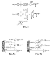
- Figures 4 depicts a functional circuit diagram, a detailed electrical circuit diagram and the waveforms on the pad (A), on the intermediate node (B) between the two cascaded inverters and on the driven metal line (C), respectively.
- the load driven by an input buffer is represented by the metal line that distributes the external control signal to a plurality of output data buffers or to a plurality of input address data buffers and which has a non-negligible capacitance because of the cumulative gate load driven as well as because the metal line must necessarily be sufficiently large in order not to introduce an intolerable intrinsic delay (excessively resistive) in the propagation of the CLK signal.
- the two cascaded inverters that constitute an input buffer cannot be of minimal size but at least the second inverter must necessarily be dimensioned such to be able to satisfactorily drive the relatively large load as noted above.
- increasing the size of the inverters could slow down the propagation of the signal onto the capacitive metal line (Heavy load), practically determining a waveform as indicated by the curve C at the bottom of Figure 4.
- the cumulative delay contributions (T1 + T2) introduced by an input buffer and by the metal line that distributes the buffered external control signal to a plurality of synchronizing and/or enabling circuits for performing a transfer of data can be significantly reduced by having the external signal applied on a pad distributed unbuffered through a metal line of sufficiently large size (conductivity) such to introduce a negligible intrinsic propagation delay, though fulfilling the specified maximum admitted input pad capacitance, and by realizing locally dedicated input buffers to each of a plurality of synchronizing and/or enabling circuits of data transfer of the integrated device for applying thereto a buffered replica of the external signal present on said distributing metal line.
- the delay contribution (T2) due to the signal distribution metal line can be significantly reduced, in many cases practically halved, by the possibility of realizing the distributing metal line of significantly increased size and that also the delay contribution (T1) imputed to an input buffer for producing a buffered replica of the external signal applied on the pad, may be even more sensibly reduced, often to about 1/3 or even 1/6 by virtue of the fact that each locally realized small size input buffer must drive a single flip-flop (FF) or a single enabling node of a controlled inverter and is not burdened by a large parasitic capacitance because of the shortness of the metal connection to the controlled node.
- FF flip-flop
- the novel input/output architecture significantly reduces these delay contributions, improving both the data output speed as well as the input (access) times.
- the architecture contemplates as usual the presence of ESD protections which, in case of parallel protection devices such as the reverse biased junctions (diodes) as shown in Figures 5A and 5B they are commonly realized near the input pad, while in case of serial type protection devices they will be as usual delocalized and replicated for the number of users of the input signal according to common practices.
- parallel protection devices such as the reverse biased junctions (diodes) as shown in Figures 5A and 5B they are commonly realized near the input pad
- serial type protection devices they will be as usual delocalized and replicated for the number of users of the input signal according to common practices.
- the size (width) of the low resistance distribution metal line, Fast Wire must be compatible with the specifications of maximum tolerable input capacitance of the integrated device.
- the power capabilities of the output buffers of the user device that issues the external control signal are exploited to charge the relatively heavy load constituted by the distributing metal line (Fast Wire) of the integrated circuit thus propagating the externally generated control signal very rapidly, without buffering it with an appropriately dimensioned input buffer.
- the necessary decoupling of the integrated circuit from the external world is implemented locally by a plurality of relatively small size (thus intrinsically fast) input buffers, each controlling a respective flip-flop or enabling node of one of the two inverters constituting a local controlled buffer.
- the output buffer of an external user already drives a relatively heavy load represented typically by a printed circuit board (PCB) metal line that could typically be of the order of 15-30 pF, depending on the length of the connection line on the PCB, and an additional capacitive load in the order of 0.5-1.0 pF, as constituted by an input signal distribution metal line, even if over dimensioned, of the integrated circuit, has hardly any significance on the design of the output buffer of the external user.
- PCB printed circuit board
Landscapes
- Physics & Mathematics (AREA)
- Nonlinear Science (AREA)
- Design And Manufacture Of Integrated Circuits (AREA)
- Semiconductor Integrated Circuits (AREA)
Priority Applications (3)
| Application Number | Priority Date | Filing Date | Title |
|---|---|---|---|
| EP06425173A EP1835618A1 (de) | 2006-03-16 | 2006-03-16 | Zeitreduzierung bei der Ausführung einer extern gesteuerten Datenübertragung bei einer integrierten Vorrichtung |
| CNA2007100885838A CN101038782A (zh) | 2006-03-16 | 2007-03-16 | 用于减少执行外部命令的数据传送的时间的方法 |
| US11/687,353 US7567107B2 (en) | 2006-03-16 | 2007-03-16 | Reduction of the time for executing an externally commanded transfer of data in an integrated device |
Applications Claiming Priority (1)
| Application Number | Priority Date | Filing Date | Title |
|---|---|---|---|
| EP06425173A EP1835618A1 (de) | 2006-03-16 | 2006-03-16 | Zeitreduzierung bei der Ausführung einer extern gesteuerten Datenübertragung bei einer integrierten Vorrichtung |
Publications (1)
| Publication Number | Publication Date |
|---|---|
| EP1835618A1 true EP1835618A1 (de) | 2007-09-19 |
Family
ID=36897209
Family Applications (1)
| Application Number | Title | Priority Date | Filing Date |
|---|---|---|---|
| EP06425173A Withdrawn EP1835618A1 (de) | 2006-03-16 | 2006-03-16 | Zeitreduzierung bei der Ausführung einer extern gesteuerten Datenübertragung bei einer integrierten Vorrichtung |
Country Status (3)
| Country | Link |
|---|---|
| US (1) | US7567107B2 (de) |
| EP (1) | EP1835618A1 (de) |
| CN (1) | CN101038782A (de) |
Citations (7)
| Publication number | Priority date | Publication date | Assignee | Title |
|---|---|---|---|---|
| US4855619A (en) * | 1987-11-17 | 1989-08-08 | Xilinx, Inc. | Buffered routing element for a user programmable logic device |
| US5124578A (en) * | 1990-10-01 | 1992-06-23 | Rockwell International Corporation | Receiver designed with large output drive and having unique input protection circuit |
| US5164817A (en) * | 1991-08-14 | 1992-11-17 | Vlsi Technology, Inc. | Distributed clock tree scheme in semiconductor packages |
| US6040203A (en) * | 1996-08-20 | 2000-03-21 | International Business Machines Corporation | Clock skew minimization and method for integrated circuits |
| US6260181B1 (en) | 1998-05-07 | 2001-07-10 | Oki Electric Industry Co., Ltd. | Integrated circuit and the design method thereof |
| US6333661B1 (en) | 1998-09-25 | 2001-12-25 | Kabushiki Kaisha Toshiba | Insulated-gate transistor signal input device |
| US20030212971A1 (en) * | 2002-05-08 | 2003-11-13 | Richard S. Rodgers | Method and apparatus for minimizing clock skew in a balanced tree when interfacing to an unblalanced load |
Family Cites Families (2)
| Publication number | Priority date | Publication date | Assignee | Title |
|---|---|---|---|---|
| FR2773020B1 (fr) * | 1997-12-24 | 2000-03-10 | Sgs Thomson Microelectronics | Circuit de distribution d'horloge dans un circuit integre |
| US6879185B2 (en) * | 2002-04-05 | 2005-04-12 | Stmicroelectronics Pvt. Ltd. | Low power clock distribution scheme |
-
2006
- 2006-03-16 EP EP06425173A patent/EP1835618A1/de not_active Withdrawn
-
2007
- 2007-03-16 US US11/687,353 patent/US7567107B2/en not_active Expired - Fee Related
- 2007-03-16 CN CNA2007100885838A patent/CN101038782A/zh active Pending
Patent Citations (7)
| Publication number | Priority date | Publication date | Assignee | Title |
|---|---|---|---|---|
| US4855619A (en) * | 1987-11-17 | 1989-08-08 | Xilinx, Inc. | Buffered routing element for a user programmable logic device |
| US5124578A (en) * | 1990-10-01 | 1992-06-23 | Rockwell International Corporation | Receiver designed with large output drive and having unique input protection circuit |
| US5164817A (en) * | 1991-08-14 | 1992-11-17 | Vlsi Technology, Inc. | Distributed clock tree scheme in semiconductor packages |
| US6040203A (en) * | 1996-08-20 | 2000-03-21 | International Business Machines Corporation | Clock skew minimization and method for integrated circuits |
| US6260181B1 (en) | 1998-05-07 | 2001-07-10 | Oki Electric Industry Co., Ltd. | Integrated circuit and the design method thereof |
| US6333661B1 (en) | 1998-09-25 | 2001-12-25 | Kabushiki Kaisha Toshiba | Insulated-gate transistor signal input device |
| US20030212971A1 (en) * | 2002-05-08 | 2003-11-13 | Richard S. Rodgers | Method and apparatus for minimizing clock skew in a balanced tree when interfacing to an unblalanced load |
Also Published As
| Publication number | Publication date |
|---|---|
| US20070216449A1 (en) | 2007-09-20 |
| US7567107B2 (en) | 2009-07-28 |
| CN101038782A (zh) | 2007-09-19 |
Similar Documents
| Publication | Publication Date | Title |
|---|---|---|
| US7061823B2 (en) | Limited output address register technique providing selectively variable write latency in DDR2 (double data rate two) integrated circuit memory devices | |
| US6970010B2 (en) | Apparatus and method for power efficient line driver | |
| US6737891B2 (en) | Tri-directional, high-speed bus switch | |
| US6205082B1 (en) | LSI device with memory and logics mounted thereon | |
| US7236035B2 (en) | Semiconductor device adapted to minimize clock skew | |
| US8897083B1 (en) | Memory interface circuitry with data strobe signal sharing capabilities | |
| JP2003050738A (ja) | キャリブレーション方法及びメモリシステム | |
| US20060132210A1 (en) | Wide-range programmable delay line | |
| US5994924A (en) | Clock distribution network with dual wire routing | |
| JPS60191497A (ja) | スタテイツクランダムアクセスメモリ | |
| JP4251692B2 (ja) | 集積回路設計方法 | |
| EP1366495B1 (de) | Schneller signalweg und verfahren | |
| EP1835618A1 (de) | Zeitreduzierung bei der Ausführung einer extern gesteuerten Datenübertragung bei einer integrierten Vorrichtung | |
| US7099170B1 (en) | Reduced turn-on current content addressable memory (CAM) device and method | |
| CN1992070B (zh) | 缓冲器控制电路及其控制方法、以及半导体存储器件 | |
| US6529442B1 (en) | Memory controller with AC power reduction through non-return-to-idle of address and control signals | |
| US6144224A (en) | Clock distribution network with dual wire routing | |
| US6822908B1 (en) | Synchronous up/down address generator for burst mode read | |
| KR100426761B1 (ko) | 반도체 집적 회로 장치 | |
| US7672190B1 (en) | Input latch circuit and method | |
| US8687442B1 (en) | Delay matching across semiconductor devices using input/output pads | |
| US20070210846A1 (en) | Inverter gate delay line with delay adjustment circuit | |
| TWI504148B (zh) | 記憶體系統 | |
| US20070024339A1 (en) | High resolution delay line architecture | |
| JP2011170919A (ja) | 半導体集積回路 |
Legal Events
| Date | Code | Title | Description |
|---|---|---|---|
| PUAI | Public reference made under article 153(3) epc to a published international application that has entered the european phase |
Free format text: ORIGINAL CODE: 0009012 |
|
| AK | Designated contracting states |
Kind code of ref document: A1 Designated state(s): AT BE BG CH CY CZ DE DK EE ES FI FR GB GR HU IE IS IT LI LT LU LV MC NL PL PT RO SE SI SK TR |
|
| AX | Request for extension of the european patent |
Extension state: AL BA HR MK YU |
|
| 17P | Request for examination filed |
Effective date: 20080229 |
|
| 17Q | First examination report despatched |
Effective date: 20080402 |
|
| AKX | Designation fees paid |
Designated state(s): DE FR GB IT |
|
| RAP1 | Party data changed (applicant data changed or rights of an application transferred) |
Owner name: STMICROELECTRONICS SRL |
|
| STAA | Information on the status of an ep patent application or granted ep patent |
Free format text: STATUS: THE APPLICATION IS DEEMED TO BE WITHDRAWN |
|
| 18D | Application deemed to be withdrawn |
Effective date: 20111001 |