EP1834508B1 - Kommunikationsdioden-treiberschaltung - Google Patents
Kommunikationsdioden-treiberschaltung Download PDFInfo
- Publication number
- EP1834508B1 EP1834508B1 EP05718890A EP05718890A EP1834508B1 EP 1834508 B1 EP1834508 B1 EP 1834508B1 EP 05718890 A EP05718890 A EP 05718890A EP 05718890 A EP05718890 A EP 05718890A EP 1834508 B1 EP1834508 B1 EP 1834508B1
- Authority
- EP
- European Patent Office
- Prior art keywords
- voltage
- led
- digital data
- drive current
- circuit
- Prior art date
- Legal status (The legal status is an assumption and is not a legal conclusion. Google has not performed a legal analysis and makes no representation as to the accuracy of the status listed.)
- Expired - Lifetime
Links
Images


Classifications
-
- H—ELECTRICITY
- H04—ELECTRIC COMMUNICATION TECHNIQUE
- H04B—TRANSMISSION
- H04B10/00—Transmission systems employing electromagnetic waves other than radio-waves, e.g. infrared, visible or ultraviolet light, or employing corpuscular radiation, e.g. quantum communication
- H04B10/11—Arrangements specific to free-space transmission, i.e. transmission through air or vacuum
- H04B10/114—Indoor or close-range type systems
- H04B10/1141—One-way transmission
-
- H—ELECTRICITY
- H04—ELECTRIC COMMUNICATION TECHNIQUE
- H04B—TRANSMISSION
- H04B10/00—Transmission systems employing electromagnetic waves other than radio-waves, e.g. infrared, visible or ultraviolet light, or employing corpuscular radiation, e.g. quantum communication
- H04B10/11—Arrangements specific to free-space transmission, i.e. transmission through air or vacuum
- H04B10/114—Indoor or close-range type systems
- H04B10/116—Visible light communication
-
- H—ELECTRICITY
- H05—ELECTRIC TECHNIQUES NOT OTHERWISE PROVIDED FOR
- H05B—ELECTRIC HEATING; ELECTRIC LIGHT SOURCES NOT OTHERWISE PROVIDED FOR; CIRCUIT ARRANGEMENTS FOR ELECTRIC LIGHT SOURCES, IN GENERAL
- H05B45/00—Circuit arrangements for operating light-emitting diodes [LED]
-
- H—ELECTRICITY
- H05—ELECTRIC TECHNIQUES NOT OTHERWISE PROVIDED FOR
- H05B—ELECTRIC HEATING; ELECTRIC LIGHT SOURCES NOT OTHERWISE PROVIDED FOR; CIRCUIT ARRANGEMENTS FOR ELECTRIC LIGHT SOURCES, IN GENERAL
- H05B45/00—Circuit arrangements for operating light-emitting diodes [LED]
- H05B45/10—Controlling the intensity of the light
-
- H—ELECTRICITY
- H05—ELECTRIC TECHNIQUES NOT OTHERWISE PROVIDED FOR
- H05B—ELECTRIC HEATING; ELECTRIC LIGHT SOURCES NOT OTHERWISE PROVIDED FOR; CIRCUIT ARRANGEMENTS FOR ELECTRIC LIGHT SOURCES, IN GENERAL
- H05B45/00—Circuit arrangements for operating light-emitting diodes [LED]
- H05B45/10—Controlling the intensity of the light
- H05B45/14—Controlling the intensity of the light using electrical feedback from LEDs or from LED modules
-
- H—ELECTRICITY
- H05—ELECTRIC TECHNIQUES NOT OTHERWISE PROVIDED FOR
- H05B—ELECTRIC HEATING; ELECTRIC LIGHT SOURCES NOT OTHERWISE PROVIDED FOR; CIRCUIT ARRANGEMENTS FOR ELECTRIC LIGHT SOURCES, IN GENERAL
- H05B45/00—Circuit arrangements for operating light-emitting diodes [LED]
- H05B45/30—Driver circuits
- H05B45/37—Converter circuits
Definitions
- the integrating unit 26 includes a switch 39 operated by the toggle unit 24, and a memory device 41 for providing the shift voltage SV(t) to the shift amplifier 22.
- the memory device 41 includes a capacitive memory component 42 selectively strapped between the shift voltage limiter 27 and GND to provide the shift voltage SV(t), and a resistive memory component 43 in parallel to the capacitive memory component 42.
- OFF digital control states resulting from I LED (t)>I N open the switch 39 to swiftly discharge the capacitive memory component 42 to decrease the shift voltage SV(t) via the resistive memory component 43.
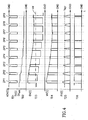
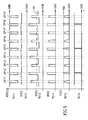
- FIG. 4 shows six Timing Diagrams TD1-TD6 at six circuit points labeled A, B, C, D, B and F for demonstrating the transient state response of the CLEC 11 to nine digital data pulses DP1, DP2, DP3, ...., DP9 pursuant to a long absence of incoming digital data pulses.
- the liming Diagram TD1 shows the analog data voltage ADV(t) at the circuit point A corresponding to the arrival of the nine digital data pulses.
- the Timing Diagram TD2 shows the shift voltage SV(t) at the circuit point B periodically decreasing stepwise from its maximum value SV max corresponding to the arrival of the nine digital data pulses.
- Timing Diagram TD 15 shows how the LED drive current I LED (t) stabilizes around the nominal LED drive current I N within a small tolerance, as evidenced by the feedback voltage FV(t) being generally smaller than the reference voltage V REF , whereupon the shift voltage SV(t) slightly increases (see Timing Diagram TD12) but is cyclically greater than same whereupon the toggle unit 24 issues OFF digital control states to periodically open the switch 39 (see Timing Diagram TD16) for causing slights drops in the shift voltage SV(t) (see Timing Diagram TD12).
Landscapes
- Physics & Mathematics (AREA)
- Electromagnetism (AREA)
- Engineering & Computer Science (AREA)
- Computer Networks & Wireless Communication (AREA)
- Signal Processing (AREA)
- Optical Communication System (AREA)
- Circuit Arrangement For Electric Light Sources In General (AREA)
- Electronic Switches (AREA)
- Led Devices (AREA)
- Input Circuits Of Receivers And Coupling Of Receivers And Audio Equipment (AREA)
- Near-Field Transmission Systems (AREA)
Claims (7)
- Kommunikationsdiodentreiberschaltung (CDDC) (10) zum selektiven Beleuchten von wenigstens einer Kommunikationsdiode (CD) (16) als Reaktion auf eingehende digitale Datenimpulse, wobei die Kommunikationsdiodentreiberschaltung (10) Folgendes umfasst:wenigstens eine Kommunikationslichtemitterschaltung (CLEC) (11) mit einem Kommunikationslichtemitterzweig (CLEB) (14) mit wenigstens einer CD (16) und so ausgelegt, dass sie den genannten CLEB (14) mit einem theoretischen LED-Ansteuerungsstrom IN ansteuert, um die genannte wenigstens eine CD (16) selektiv zu beleuchten,wobei jede CLEC (11) der genannten wenigstens einen CLEC eine Treibereinheit (13) beinhaltet, die einen Verschiebungsverstärker zum algebraischen Überlagerungsaddieren einer pulsierten analogen Datenspannung ADV(t), die den eingehenden digitalen Datenimpulsen entspricht, und einer variablen Verschiebungsspannung Sv(t) zum Ausgeben einer pulsierten Ansteuerungsspannung DV(t) zum Ansteuern des genannten CLEB (14) mit einem pulsierten LED-Ansteuerungsstrom ILED(t) umfasst, um die genannte wenigstens eine CD (16) im Einklang mit den eingehenden digitalen Datenimpulsen selektiv zu beleuchten, und
wobei jede CLEC (11) der genannten wenigstens einen CLEC eine Regelkreisrückmeldeeinheit (18) zum Abgreifen des genannten CLEB aufweist,
dadurch gekennzeichnet, dass die Regelkreisrückmeldeeinheit (18) zum kontinuierlichen Überwachen einer pulsierten Überwachungsspannung MV(t) direkt proportional zu dem genannten LED-Ansteuerungsstrom ILED(t) konfiguriert ist, um die genannte Verschiebungsspannung SV(t) bis zu einer maximalen Verschiebungsspannung SVmax zu erhöhen, die geringer ist als eine Schwellenansteuerungsspannung, um die genannte wenigstens eine CD (16) nach einer langen Zeit ohne eingehende digitale Datenimpulse kontinuierlich zu beleuchten, mit Ausnahme einer intermittierenden, schrittweisen Abnahme der genannten Verschiebungsspannung SV(t) als Reaktion darauf, dass jeder einzelne eingehende digitale Datenimpuls dazu beiträgt, dass ein LED-Ansteuerungsstrom ILED (t) die Bedingung ILED(t)>IN erfüllt. - Schaltung (10) nach Anspruch 1, wobei die genannte Rückmeldeeinheit (18) eine Umschalteinheit (24) mit einem Komparator (33) zum Vergleichen einer von der genannten Überwachungsspannung MV(t) abgeleiteten Rückmeldespannung FV(t) mit einer Referenzspannung VREF proportional zum theoretischen LED-Ansteuerungsstrom IN aufweist, um einen digitalen Einschaltsteuerzustand unter der Bedingung ILED(t) <IN und einen entgegengesetzten digitalen Ausschaltsteuerzustand als Reaktion auf jeden einzelnen eingehenden digitalen Datenimpuls auszugeben, der dazu beiträgt, dass ein LED-Ansteuerungsstrom ILED(t) die Bedingung ILED (t) >IN erfüllt.
- Schaltung (10) nach Anspruch 2, wobei die genannte Umschalteinheit (24) ferner ein Tiefpassfilter (LPF) (32) zum Formen von allgemein rechteckigen Impulsen der genannten Überwachungsspannung MV(t) zu allgemein dreieckigen Spannungsimpulsen aufweist, um die Dauer zu bestimmen, für die die genannte Umschalteinheit (24) die genannten entgegengesetzten digitalen Steuerzustände unter der Bedingung ILED (t) >IN ausgibt.
- Schaltung (10) nach einem der Ansprüche 1 bis 3, wobei die genannte Rückmeldeeinheit (18) eine Integriereinheit (26) mit einem Speichergerät (41) aufweist, um die genannte Verschiebungsspannung SV(t) zu erzeugen, wobei das genannte Speichergerät (41) eine Speicherkomponente (42) zum kontinuierlichen Erhöhen der genannten Verschiebungsspannung SV(t) unter der Bedingung ILED(t)<IN aufweist.
- Schaltung (10) nach Anspruch 4, wobei die genannte Speicherkomponente (42) eine kapazitive Speicherkomponente ist.
- Schaltung (10) nach Anspruch 5, wobei das genannte Speichergerät (41) eine Widerstandsspeicherkomponente (43) zum selektiven Entladen der genannten kapazitiven Speicherkomponente unter der Bedingung ILED(t)>IN aufweist.
- Schaltung (10) nach einem der Ansprüche 1 bis 6, wobei der genannte CLEB (14) einen an Masse gebundenen Abtastwiderstand (17) aufweist und die genannte Umschalteinheit (24) den genannten Abtastwiderstand (17) anzapft, um die genannte Überwachungsspannung MV(t) kontinuierlich zu überwachen.
Applications Claiming Priority (2)
| Application Number | Priority Date | Filing Date | Title |
|---|---|---|---|
| US64189605P | 2005-01-06 | 2005-01-06 | |
| PCT/IL2005/000317 WO2006072929A1 (en) | 2005-01-06 | 2005-03-20 | Communication diode driver circuit |
Publications (2)
| Publication Number | Publication Date |
|---|---|
| EP1834508A1 EP1834508A1 (de) | 2007-09-19 |
| EP1834508B1 true EP1834508B1 (de) | 2008-11-12 |
Family
ID=34963201
Family Applications (1)
| Application Number | Title | Priority Date | Filing Date |
|---|---|---|---|
| EP05718890A Expired - Lifetime EP1834508B1 (de) | 2005-01-06 | 2005-03-20 | Kommunikationsdioden-treiberschaltung |
Country Status (8)
| Country | Link |
|---|---|
| US (1) | US7570235B2 (de) |
| EP (1) | EP1834508B1 (de) |
| JP (1) | JP4755187B2 (de) |
| CN (1) | CN100553390C (de) |
| AT (1) | ATE414401T1 (de) |
| CA (1) | CA2576711C (de) |
| DE (1) | DE602005011053D1 (de) |
| WO (1) | WO2006072929A1 (de) |
Families Citing this family (8)
| Publication number | Priority date | Publication date | Assignee | Title |
|---|---|---|---|---|
| EP2219305B1 (de) * | 2007-10-24 | 2018-11-07 | Kabushiki Kaisha Audio-Technica | Infrarotsender |
| EP2101424B1 (de) | 2008-03-10 | 2013-02-27 | Siemens Aktiengesellschaft | Verfahren und Vorrichtung zur optischen Übertragung von Daten |
| US7952293B2 (en) * | 2008-04-30 | 2011-05-31 | Lsi Industries, Inc. | Power factor correction and driver circuits |
| US8432108B2 (en) * | 2008-04-30 | 2013-04-30 | Lsi Industries, Inc. | Solid state lighting, driver circuits, and related software |
| US7994730B2 (en) * | 2009-06-04 | 2011-08-09 | Apple Inc. | Pulse width modulation (PWM) closed loop LED current driver in an embedded system |
| US8912732B2 (en) | 2010-06-10 | 2014-12-16 | Maxim Integrated Products, Inc. | Current sensing for LED drivers |
| US8917034B2 (en) * | 2012-05-31 | 2014-12-23 | Fairchild Semiconductor Corporation | Current overshoot limiting circuit |
| DE102013222177A1 (de) * | 2013-10-31 | 2015-04-30 | Tridonic Gmbh & Co Kg | Leuchtmittel-Betriebsschaltung mit getaktetem Konverter zum digitalen Einstellen einer Farbtemperatur und/oder eines Dimmpegels |
Family Cites Families (25)
| Publication number | Priority date | Publication date | Assignee | Title |
|---|---|---|---|---|
| JPS59112670A (ja) | 1982-12-20 | 1984-06-29 | Hitachi Ltd | 光デイジタル送信器における出力安定化回路 |
| JPS60113546A (ja) * | 1983-11-24 | 1985-06-20 | Nec Corp | 光送信器 |
| JPS60148182A (ja) * | 1984-01-13 | 1985-08-05 | Toshiba Corp | バ−スト光出力安定化駆動方式 |
| GB2162399B (en) | 1984-07-25 | 1987-10-14 | Stc Plc | Led modulator |
| JPS62217687A (ja) * | 1986-03-19 | 1987-09-25 | Fujitsu Ltd | レ−ザダイオ−ド駆動装置 |
| JPS63110685A (ja) | 1986-10-28 | 1988-05-16 | Sumitomo Electric Ind Ltd | 発光素子の駆動回路 |
| JPS63229791A (ja) * | 1987-03-18 | 1988-09-26 | Mitsubishi Rayon Co Ltd | 発光素子駆動回路 |
| US5329210A (en) * | 1991-11-13 | 1994-07-12 | At&T Bell Laboratories | High-speed driver for an LED communication system or the like |
| JPH07273388A (ja) * | 1994-03-28 | 1995-10-20 | Furukawa Electric Co Ltd:The | 光送信器 |
| JP3457763B2 (ja) * | 1995-04-13 | 2003-10-20 | アルプス電気株式会社 | 発光素子駆動回路 |
| SE519550C2 (sv) * | 1997-01-03 | 2003-03-11 | Ericsson Telefon Ab L M | Drivkrets samt förfarande för att driva en sådan drivkrets |
| JP2000277847A (ja) * | 1999-03-26 | 2000-10-06 | Hitachi Koki Co Ltd | 半導体レーザ駆動装置 |
| DE19930174A1 (de) * | 1999-06-30 | 2001-01-04 | Patent Treuhand Ges Fuer Elektrische Gluehlampen Mbh | Ansteuerschaltung für LED und zugehöriges Betriebsverfahren |
| DE19946218C1 (de) * | 1999-09-27 | 2001-01-25 | Fraunhofer Ges Forschung | Treiberschaltung für ein elektronisches Datenübertragungsbauglied |
| US6362578B1 (en) * | 1999-12-23 | 2002-03-26 | Stmicroelectronics, Inc. | LED driver circuit and method |
| JP2001223430A (ja) * | 2000-02-09 | 2001-08-17 | Ricoh Opt Ind Co Ltd | 半導体レーザ駆動装置 |
| US20010033503A1 (en) * | 2000-03-28 | 2001-10-25 | Hamp Charles Henry | Low power lighting system with LED illumination |
| US20030041620A1 (en) * | 2001-08-30 | 2003-03-06 | Martin Gruber | Non-rectangular multistone jewelry |
| JP2003101123A (ja) | 2001-09-20 | 2003-04-04 | Kyocera Corp | 光半導体素子収納用パッケージ |
| GB2381138B (en) | 2001-10-17 | 2005-06-29 | Matsushita Comm Ind Uk Ltd | Driver circuit for light emitting devices |
| US6586890B2 (en) * | 2001-12-05 | 2003-07-01 | Koninklijke Philips Electronics N.V. | LED driver circuit with PWM output |
| US6853150B2 (en) * | 2001-12-28 | 2005-02-08 | Koninklijke Philips Electronics N.V. | Light emitting diode driver |
| JP4043844B2 (ja) * | 2002-05-24 | 2008-02-06 | フリースケール セミコンダクター インコーポレイテッド | 発光素子駆動装置 |
| CN100501827C (zh) * | 2003-03-15 | 2009-06-17 | 鸿富锦精密工业(深圳)有限公司 | 发光二极管驱动装置及其驱动方法 |
| US7307614B2 (en) * | 2004-04-29 | 2007-12-11 | Micrel Inc. | Light emitting diode driver circuit |
-
2005
- 2005-03-20 CN CNB200580035105XA patent/CN100553390C/zh not_active Expired - Fee Related
- 2005-03-20 AT AT05718890T patent/ATE414401T1/de not_active IP Right Cessation
- 2005-03-20 US US10/576,343 patent/US7570235B2/en not_active Expired - Fee Related
- 2005-03-20 DE DE602005011053T patent/DE602005011053D1/de not_active Expired - Lifetime
- 2005-03-20 JP JP2007534171A patent/JP4755187B2/ja not_active Expired - Fee Related
- 2005-03-20 WO PCT/IL2005/000317 patent/WO2006072929A1/en not_active Ceased
- 2005-03-20 CA CA2576711A patent/CA2576711C/en not_active Expired - Fee Related
- 2005-03-20 EP EP05718890A patent/EP1834508B1/de not_active Expired - Lifetime
Also Published As
| Publication number | Publication date |
|---|---|
| CA2576711A1 (en) | 2006-07-13 |
| US7570235B2 (en) | 2009-08-04 |
| US20070104075A1 (en) | 2007-05-10 |
| DE602005011053D1 (de) | 2008-12-24 |
| JP2008515218A (ja) | 2008-05-08 |
| JP4755187B2 (ja) | 2011-08-24 |
| CA2576711C (en) | 2010-04-13 |
| CN101040568A (zh) | 2007-09-19 |
| EP1834508A1 (de) | 2007-09-19 |
| CN100553390C (zh) | 2009-10-21 |
| ATE414401T1 (de) | 2008-11-15 |
| WO2006072929A1 (en) | 2006-07-13 |
Similar Documents
| Publication | Publication Date | Title |
|---|---|---|
| US7944420B2 (en) | Light emitting diode driver providing current and power control | |
| US6044095A (en) | Light emitting device drive circuit | |
| CA2576711C (en) | Communication diode driver circuit | |
| US20160044760A1 (en) | Method and Apparatus for Precise Temperature Brightness Compensation of LED | |
| US5499258A (en) | Automatic temperature control circuit of laser diode and electric/optical signal converting unit using the same | |
| WO2007137087A2 (en) | Integrated programmable over-current protection circuit for optical transmitters | |
| EP3519879B1 (de) | Vorrichtung und verfahren zur steuerung eines led-lichtstroms | |
| JP2004299102A (ja) | 照明装置とそれに用いる照明ヘッド及び電源装置 | |
| US7994730B2 (en) | Pulse width modulation (PWM) closed loop LED current driver in an embedded system | |
| US8441195B2 (en) | Illumination adjustment circuit | |
| WO2001076023A2 (en) | Digital laser driver circuit | |
| EP3095301B1 (de) | Eine schaltungsanordnung zum betreiben von led-ketten | |
| KR20140085103A (ko) | 디밍 조절 및 포워드 전압 제어를 이용한 피드백 제어 회로 및 전원 장치 | |
| JP5929687B2 (ja) | 発光素子駆動回路 | |
| JPH04152582A (ja) | 光送信器 | |
| US9101024B2 (en) | Smart FET circuit | |
| JP6486606B2 (ja) | Ledアレイ駆動回路 | |
| JP2006235767A (ja) | リミッタ付電流制御回路 | |
| KR101611588B1 (ko) | Led 구동 장치 | |
| US8431882B2 (en) | Light-receiving circuit and semiconductor device having same | |
| CN102291866A (zh) | 灯具控制电路 | |
| JP6241169B2 (ja) | 通信装置及び通信システム、並びに通信方法 | |
| JPH0191484A (ja) | 発光素子駆動回路 | |
| JPH0340531A (ja) | 光送信器 | |
| JPH058967U (ja) | 光送信器 |
Legal Events
| Date | Code | Title | Description |
|---|---|---|---|
| PUAI | Public reference made under article 153(3) epc to a published international application that has entered the european phase |
Free format text: ORIGINAL CODE: 0009012 |
|
| 17P | Request for examination filed |
Effective date: 20070320 |
|
| AK | Designated contracting states |
Kind code of ref document: A1 Designated state(s): AT BE BG CH CY CZ DE DK EE ES FI FR GB GR HU IE IS IT LI LT LU MC NL PL PT RO SE SI SK TR |
|
| 17Q | First examination report despatched |
Effective date: 20071025 |
|
| DAX | Request for extension of the european patent (deleted) | ||
| GRAP | Despatch of communication of intention to grant a patent |
Free format text: ORIGINAL CODE: EPIDOSNIGR1 |
|
| GRAS | Grant fee paid |
Free format text: ORIGINAL CODE: EPIDOSNIGR3 |
|
| GRAA | (expected) grant |
Free format text: ORIGINAL CODE: 0009210 |
|
| AK | Designated contracting states |
Kind code of ref document: B1 Designated state(s): AT BE BG CH CY CZ DE DK EE ES FI FR GB GR HU IE IS IT LI LT LU MC NL PL PT RO SE SI SK TR |
|
| REG | Reference to a national code |
Ref country code: GB Ref legal event code: FG4D |
|
| REG | Reference to a national code |
Ref country code: CH Ref legal event code: EP |
|
| REG | Reference to a national code |
Ref country code: IE Ref legal event code: FG4D |
|
| REF | Corresponds to: |
Ref document number: 602005011053 Country of ref document: DE Date of ref document: 20081224 Kind code of ref document: P |
|
| LTIE | Lt: invalidation of european patent or patent extension |
Effective date: 20081112 |
|
| PG25 | Lapsed in a contracting state [announced via postgrant information from national office to epo] |
Ref country code: AT Free format text: LAPSE BECAUSE OF FAILURE TO SUBMIT A TRANSLATION OF THE DESCRIPTION OR TO PAY THE FEE WITHIN THE PRESCRIBED TIME-LIMIT Effective date: 20081112 Ref country code: LT Free format text: LAPSE BECAUSE OF FAILURE TO SUBMIT A TRANSLATION OF THE DESCRIPTION OR TO PAY THE FEE WITHIN THE PRESCRIBED TIME-LIMIT Effective date: 20081112 Ref country code: ES Free format text: LAPSE BECAUSE OF FAILURE TO SUBMIT A TRANSLATION OF THE DESCRIPTION OR TO PAY THE FEE WITHIN THE PRESCRIBED TIME-LIMIT Effective date: 20090223 |
|
| NLV1 | Nl: lapsed or annulled due to failure to fulfill the requirements of art. 29p and 29m of the patents act | ||
| PG25 | Lapsed in a contracting state [announced via postgrant information from national office to epo] |
Ref country code: SI Free format text: LAPSE BECAUSE OF FAILURE TO SUBMIT A TRANSLATION OF THE DESCRIPTION OR TO PAY THE FEE WITHIN THE PRESCRIBED TIME-LIMIT Effective date: 20081112 Ref country code: PL Free format text: LAPSE BECAUSE OF FAILURE TO SUBMIT A TRANSLATION OF THE DESCRIPTION OR TO PAY THE FEE WITHIN THE PRESCRIBED TIME-LIMIT Effective date: 20081112 Ref country code: NL Free format text: LAPSE BECAUSE OF FAILURE TO SUBMIT A TRANSLATION OF THE DESCRIPTION OR TO PAY THE FEE WITHIN THE PRESCRIBED TIME-LIMIT Effective date: 20081112 Ref country code: IS Free format text: LAPSE BECAUSE OF FAILURE TO SUBMIT A TRANSLATION OF THE DESCRIPTION OR TO PAY THE FEE WITHIN THE PRESCRIBED TIME-LIMIT Effective date: 20090312 Ref country code: FI Free format text: LAPSE BECAUSE OF FAILURE TO SUBMIT A TRANSLATION OF THE DESCRIPTION OR TO PAY THE FEE WITHIN THE PRESCRIBED TIME-LIMIT Effective date: 20081112 |
|
| PG25 | Lapsed in a contracting state [announced via postgrant information from national office to epo] |
Ref country code: EE Free format text: LAPSE BECAUSE OF FAILURE TO SUBMIT A TRANSLATION OF THE DESCRIPTION OR TO PAY THE FEE WITHIN THE PRESCRIBED TIME-LIMIT Effective date: 20081112 Ref country code: RO Free format text: LAPSE BECAUSE OF FAILURE TO SUBMIT A TRANSLATION OF THE DESCRIPTION OR TO PAY THE FEE WITHIN THE PRESCRIBED TIME-LIMIT Effective date: 20081112 Ref country code: DK Free format text: LAPSE BECAUSE OF FAILURE TO SUBMIT A TRANSLATION OF THE DESCRIPTION OR TO PAY THE FEE WITHIN THE PRESCRIBED TIME-LIMIT Effective date: 20081112 Ref country code: BE Free format text: LAPSE BECAUSE OF FAILURE TO SUBMIT A TRANSLATION OF THE DESCRIPTION OR TO PAY THE FEE WITHIN THE PRESCRIBED TIME-LIMIT Effective date: 20081112 Ref country code: BG Free format text: LAPSE BECAUSE OF FAILURE TO SUBMIT A TRANSLATION OF THE DESCRIPTION OR TO PAY THE FEE WITHIN THE PRESCRIBED TIME-LIMIT Effective date: 20090212 |
|
| PG25 | Lapsed in a contracting state [announced via postgrant information from national office to epo] |
Ref country code: SE Free format text: LAPSE BECAUSE OF FAILURE TO SUBMIT A TRANSLATION OF THE DESCRIPTION OR TO PAY THE FEE WITHIN THE PRESCRIBED TIME-LIMIT Effective date: 20090212 Ref country code: CZ Free format text: LAPSE BECAUSE OF FAILURE TO SUBMIT A TRANSLATION OF THE DESCRIPTION OR TO PAY THE FEE WITHIN THE PRESCRIBED TIME-LIMIT Effective date: 20081112 Ref country code: PT Free format text: LAPSE BECAUSE OF FAILURE TO SUBMIT A TRANSLATION OF THE DESCRIPTION OR TO PAY THE FEE WITHIN THE PRESCRIBED TIME-LIMIT Effective date: 20090413 |
|
| PLBE | No opposition filed within time limit |
Free format text: ORIGINAL CODE: 0009261 |
|
| STAA | Information on the status of an ep patent application or granted ep patent |
Free format text: STATUS: NO OPPOSITION FILED WITHIN TIME LIMIT |
|
| PG25 | Lapsed in a contracting state [announced via postgrant information from national office to epo] |
Ref country code: SK Free format text: LAPSE BECAUSE OF FAILURE TO SUBMIT A TRANSLATION OF THE DESCRIPTION OR TO PAY THE FEE WITHIN THE PRESCRIBED TIME-LIMIT Effective date: 20081112 |
|
| 26N | No opposition filed |
Effective date: 20090813 |
|
| PG25 | Lapsed in a contracting state [announced via postgrant information from national office to epo] |
Ref country code: MC Free format text: LAPSE BECAUSE OF NON-PAYMENT OF DUE FEES Effective date: 20090331 |
|
| REG | Reference to a national code |
Ref country code: CH Ref legal event code: PL |
|
| REG | Reference to a national code |
Ref country code: IE Ref legal event code: MM4A |
|
| PG25 | Lapsed in a contracting state [announced via postgrant information from national office to epo] |
Ref country code: CH Free format text: LAPSE BECAUSE OF NON-PAYMENT OF DUE FEES Effective date: 20090331 Ref country code: LI Free format text: LAPSE BECAUSE OF NON-PAYMENT OF DUE FEES Effective date: 20090331 Ref country code: IE Free format text: LAPSE BECAUSE OF NON-PAYMENT OF DUE FEES Effective date: 20090320 |
|
| PG25 | Lapsed in a contracting state [announced via postgrant information from national office to epo] |
Ref country code: GR Free format text: LAPSE BECAUSE OF FAILURE TO SUBMIT A TRANSLATION OF THE DESCRIPTION OR TO PAY THE FEE WITHIN THE PRESCRIBED TIME-LIMIT Effective date: 20090213 |
|
| PG25 | Lapsed in a contracting state [announced via postgrant information from national office to epo] |
Ref country code: LU Free format text: LAPSE BECAUSE OF NON-PAYMENT OF DUE FEES Effective date: 20090320 |
|
| PG25 | Lapsed in a contracting state [announced via postgrant information from national office to epo] |
Ref country code: HU Free format text: LAPSE BECAUSE OF FAILURE TO SUBMIT A TRANSLATION OF THE DESCRIPTION OR TO PAY THE FEE WITHIN THE PRESCRIBED TIME-LIMIT Effective date: 20090513 |
|
| PGFP | Annual fee paid to national office [announced via postgrant information from national office to epo] |
Ref country code: DE Payment date: 20110329 Year of fee payment: 7 Ref country code: FR Payment date: 20110407 Year of fee payment: 7 Ref country code: GB Payment date: 20110316 Year of fee payment: 7 |
|
| PG25 | Lapsed in a contracting state [announced via postgrant information from national office to epo] |
Ref country code: TR Free format text: LAPSE BECAUSE OF FAILURE TO SUBMIT A TRANSLATION OF THE DESCRIPTION OR TO PAY THE FEE WITHIN THE PRESCRIBED TIME-LIMIT Effective date: 20081112 |
|
| PG25 | Lapsed in a contracting state [announced via postgrant information from national office to epo] |
Ref country code: CY Free format text: LAPSE BECAUSE OF FAILURE TO SUBMIT A TRANSLATION OF THE DESCRIPTION OR TO PAY THE FEE WITHIN THE PRESCRIBED TIME-LIMIT Effective date: 20081112 |
|
| PGFP | Annual fee paid to national office [announced via postgrant information from national office to epo] |
Ref country code: IT Payment date: 20110329 Year of fee payment: 7 |
|
| GBPC | Gb: european patent ceased through non-payment of renewal fee |
Effective date: 20120320 |
|
| REG | Reference to a national code |
Ref country code: FR Ref legal event code: ST Effective date: 20121130 |
|
| REG | Reference to a national code |
Ref country code: DE Ref legal event code: R119 Ref document number: 602005011053 Country of ref document: DE Effective date: 20121002 |
|
| PG25 | Lapsed in a contracting state [announced via postgrant information from national office to epo] |
Ref country code: GB Free format text: LAPSE BECAUSE OF NON-PAYMENT OF DUE FEES Effective date: 20120320 Ref country code: FR Free format text: LAPSE BECAUSE OF NON-PAYMENT OF DUE FEES Effective date: 20120402 |
|
| PG25 | Lapsed in a contracting state [announced via postgrant information from national office to epo] |
Ref country code: IT Free format text: LAPSE BECAUSE OF NON-PAYMENT OF DUE FEES Effective date: 20120320 |
|
| PG25 | Lapsed in a contracting state [announced via postgrant information from national office to epo] |
Ref country code: DE Free format text: LAPSE BECAUSE OF NON-PAYMENT OF DUE FEES Effective date: 20121002 |