EP1830405A1 - Semiconductor device - Google Patents
Semiconductor device Download PDFInfo
- Publication number
- EP1830405A1 EP1830405A1 EP05816412A EP05816412A EP1830405A1 EP 1830405 A1 EP1830405 A1 EP 1830405A1 EP 05816412 A EP05816412 A EP 05816412A EP 05816412 A EP05816412 A EP 05816412A EP 1830405 A1 EP1830405 A1 EP 1830405A1
- Authority
- EP
- European Patent Office
- Prior art keywords
- semiconductor device
- variable resistor
- temperature
- electrode
- ptc element
- Prior art date
- Legal status (The legal status is an assumption and is not a legal conclusion. Google has not performed a legal analysis and makes no representation as to the accuracy of the status listed.)
- Granted
Links
- 239000004065 semiconductor Substances 0.000 title claims abstract description 105
- 239000000463 material Substances 0.000 claims description 79
- 238000000034 method Methods 0.000 claims description 19
- 238000002844 melting Methods 0.000 claims description 11
- 230000008018 melting Effects 0.000 claims description 11
- 229910000679 solder Inorganic materials 0.000 claims description 10
- 238000007906 compression Methods 0.000 claims description 8
- 238000005219 brazing Methods 0.000 claims description 5
- 239000000155 melt Substances 0.000 claims description 2
- 230000001681 protective effect Effects 0.000 claims description 2
- 238000001514 detection method Methods 0.000 abstract description 56
- 230000008859 change Effects 0.000 abstract description 18
- 238000012544 monitoring process Methods 0.000 abstract description 7
- 230000003247 decreasing effect Effects 0.000 abstract 1
- RYGMFSIKBFXOCR-UHFFFAOYSA-N Copper Chemical compound [Cu] RYGMFSIKBFXOCR-UHFFFAOYSA-N 0.000 description 34
- 239000010410 layer Substances 0.000 description 34
- 239000011889 copper foil Substances 0.000 description 28
- 229910052782 aluminium Inorganic materials 0.000 description 24
- XAGFODPZIPBFFR-UHFFFAOYSA-N aluminium Chemical compound [Al] XAGFODPZIPBFFR-UHFFFAOYSA-N 0.000 description 24
- 230000020169 heat generation Effects 0.000 description 9
- 239000000758 substrate Substances 0.000 description 9
- VYPSYNLAJGMNEJ-UHFFFAOYSA-N Silicium dioxide Chemical compound O=[Si]=O VYPSYNLAJGMNEJ-UHFFFAOYSA-N 0.000 description 8
- 230000006378 damage Effects 0.000 description 7
- 230000007423 decrease Effects 0.000 description 7
- 229920000620 organic polymer Polymers 0.000 description 7
- PXHVJJICTQNCMI-UHFFFAOYSA-N Nickel Chemical compound [Ni] PXHVJJICTQNCMI-UHFFFAOYSA-N 0.000 description 6
- 229910052802 copper Inorganic materials 0.000 description 6
- 239000010949 copper Substances 0.000 description 6
- PCHJSUWPFVWCPO-UHFFFAOYSA-N gold Chemical compound [Au] PCHJSUWPFVWCPO-UHFFFAOYSA-N 0.000 description 6
- 229910052737 gold Inorganic materials 0.000 description 6
- 239000010931 gold Substances 0.000 description 6
- 229910052814 silicon oxide Inorganic materials 0.000 description 6
- 238000009529 body temperature measurement Methods 0.000 description 5
- 238000010586 diagram Methods 0.000 description 5
- 239000012535 impurity Substances 0.000 description 5
- 238000004519 manufacturing process Methods 0.000 description 5
- 239000002245 particle Substances 0.000 description 5
- 229910021420 polycrystalline silicon Inorganic materials 0.000 description 5
- 229920005591 polysilicon Polymers 0.000 description 5
- 230000003685 thermal hair damage Effects 0.000 description 5
- 102000004129 N-Type Calcium Channels Human genes 0.000 description 4
- 108090000699 N-Type Calcium Channels Proteins 0.000 description 4
- 229910045601 alloy Inorganic materials 0.000 description 4
- 239000000956 alloy Substances 0.000 description 4
- 239000000470 constituent Substances 0.000 description 4
- 230000000694 effects Effects 0.000 description 4
- 230000005684 electric field Effects 0.000 description 4
- -1 polyethylene Polymers 0.000 description 4
- 230000008569 process Effects 0.000 description 4
- 239000004698 Polyethylene Substances 0.000 description 3
- 239000002131 composite material Substances 0.000 description 3
- 229910052759 nickel Inorganic materials 0.000 description 3
- 229920000573 polyethylene Polymers 0.000 description 3
- 238000004088 simulation Methods 0.000 description 3
- BQCADISMDOOEFD-UHFFFAOYSA-N Silver Chemical compound [Ag] BQCADISMDOOEFD-UHFFFAOYSA-N 0.000 description 2
- GWEVSGVZZGPLCZ-UHFFFAOYSA-N Titan oxide Chemical compound O=[Ti]=O GWEVSGVZZGPLCZ-UHFFFAOYSA-N 0.000 description 2
- 238000004364 calculation method Methods 0.000 description 2
- 239000000919 ceramic Substances 0.000 description 2
- 230000006866 deterioration Effects 0.000 description 2
- 229910052748 manganese Inorganic materials 0.000 description 2
- 238000005259 measurement Methods 0.000 description 2
- 238000000465 moulding Methods 0.000 description 2
- 230000002265 prevention Effects 0.000 description 2
- 230000000630 rising effect Effects 0.000 description 2
- 229910052709 silver Inorganic materials 0.000 description 2
- 239000004332 silver Substances 0.000 description 2
- 239000002344 surface layer Substances 0.000 description 2
- UONOETXJSWQNOL-UHFFFAOYSA-N tungsten carbide Chemical compound [W+]#[C-] UONOETXJSWQNOL-UHFFFAOYSA-N 0.000 description 2
- 229910011255 B2O3 Inorganic materials 0.000 description 1
- 229910052684 Cerium Inorganic materials 0.000 description 1
- 229910052688 Gadolinium Inorganic materials 0.000 description 1
- 229910052689 Holmium Inorganic materials 0.000 description 1
- ZOKXTWBITQBERF-UHFFFAOYSA-N Molybdenum Chemical compound [Mo] ZOKXTWBITQBERF-UHFFFAOYSA-N 0.000 description 1
- 229910052779 Neodymium Inorganic materials 0.000 description 1
- 239000004743 Polypropylene Substances 0.000 description 1
- 229910052777 Praseodymium Inorganic materials 0.000 description 1
- 229910052772 Samarium Inorganic materials 0.000 description 1
- 238000010521 absorption reaction Methods 0.000 description 1
- 229910052787 antimony Inorganic materials 0.000 description 1
- 229910002113 barium titanate Inorganic materials 0.000 description 1
- 229910052797 bismuth Inorganic materials 0.000 description 1
- 239000006229 carbon black Substances 0.000 description 1
- 229910017052 cobalt Inorganic materials 0.000 description 1
- 239000010941 cobalt Substances 0.000 description 1
- GUTLYIVDDKVIGB-UHFFFAOYSA-N cobalt atom Chemical compound [Co] GUTLYIVDDKVIGB-UHFFFAOYSA-N 0.000 description 1
- 229910052681 coesite Inorganic materials 0.000 description 1
- 150000001875 compounds Chemical class 0.000 description 1
- 229920001577 copolymer Polymers 0.000 description 1
- 229910052906 cristobalite Inorganic materials 0.000 description 1
- 239000013078 crystal Substances 0.000 description 1
- JKWMSGQKBLHBQQ-UHFFFAOYSA-N diboron trioxide Chemical compound O=BOB=O JKWMSGQKBLHBQQ-UHFFFAOYSA-N 0.000 description 1
- 239000003822 epoxy resin Substances 0.000 description 1
- 230000004907 flux Effects 0.000 description 1
- 239000011521 glass Substances 0.000 description 1
- 229910052735 hafnium Inorganic materials 0.000 description 1
- 229920001903 high density polyethylene Polymers 0.000 description 1
- 230000006872 improvement Effects 0.000 description 1
- 238000009413 insulation Methods 0.000 description 1
- 229920000554 ionomer Polymers 0.000 description 1
- 229910052746 lanthanum Inorganic materials 0.000 description 1
- 229910052745 lead Inorganic materials 0.000 description 1
- HTUMBQDCCIXGCV-UHFFFAOYSA-N lead oxide Chemical compound [O-2].[Pb+2] HTUMBQDCCIXGCV-UHFFFAOYSA-N 0.000 description 1
- YEXPOXQUZXUXJW-UHFFFAOYSA-N lead(II) oxide Inorganic materials [Pb]=O YEXPOXQUZXUXJW-UHFFFAOYSA-N 0.000 description 1
- 229920001684 low density polyethylene Polymers 0.000 description 1
- 229910052751 metal Inorganic materials 0.000 description 1
- 239000002184 metal Substances 0.000 description 1
- 239000007769 metal material Substances 0.000 description 1
- 229910052750 molybdenum Inorganic materials 0.000 description 1
- 239000011733 molybdenum Substances 0.000 description 1
- 229910052758 niobium Inorganic materials 0.000 description 1
- 239000011368 organic material Substances 0.000 description 1
- 230000002093 peripheral effect Effects 0.000 description 1
- 230000000704 physical effect Effects 0.000 description 1
- 238000005498 polishing Methods 0.000 description 1
- 229920000647 polyepoxide Polymers 0.000 description 1
- 229920001155 polypropylene Polymers 0.000 description 1
- 229920002689 polyvinyl acetate Polymers 0.000 description 1
- 229940075065 polyvinyl acetate Drugs 0.000 description 1
- 239000011118 polyvinyl acetate Substances 0.000 description 1
- 229920000915 polyvinyl chloride Polymers 0.000 description 1
- 239000004800 polyvinyl chloride Substances 0.000 description 1
- 239000000843 powder Substances 0.000 description 1
- 230000009467 reduction Effects 0.000 description 1
- 239000000377 silicon dioxide Substances 0.000 description 1
- 229910052682 stishovite Inorganic materials 0.000 description 1
- 230000001629 suppression Effects 0.000 description 1
- 229910052715 tantalum Inorganic materials 0.000 description 1
- 229910052718 tin Inorganic materials 0.000 description 1
- 230000001052 transient effect Effects 0.000 description 1
- 229910052905 tridymite Inorganic materials 0.000 description 1
- WFKWXMTUELFFGS-UHFFFAOYSA-N tungsten Chemical compound [W] WFKWXMTUELFFGS-UHFFFAOYSA-N 0.000 description 1
- 229910052721 tungsten Inorganic materials 0.000 description 1
- 239000010937 tungsten Substances 0.000 description 1
- 238000007740 vapor deposition Methods 0.000 description 1
- 239000002023 wood Substances 0.000 description 1
- 229910000634 wood's metal Inorganic materials 0.000 description 1
- 229910052726 zirconium Inorganic materials 0.000 description 1
Images


Classifications
-
- H—ELECTRICITY
- H01—ELECTRIC ELEMENTS
- H01L—SEMICONDUCTOR DEVICES NOT COVERED BY CLASS H10
- H01L29/00—Semiconductor devices adapted for rectifying, amplifying, oscillating or switching, or capacitors or resistors with at least one potential-jump barrier or surface barrier, e.g. PN junction depletion layer or carrier concentration layer; Details of semiconductor bodies or of electrodes thereof ; Multistep manufacturing processes therefor
- H01L29/66—Types of semiconductor device ; Multistep manufacturing processes therefor
- H01L29/68—Types of semiconductor device ; Multistep manufacturing processes therefor controllable by only the electric current supplied, or only the electric potential applied, to an electrode which does not carry the current to be rectified, amplified or switched
- H01L29/70—Bipolar devices
- H01L29/72—Transistor-type devices, i.e. able to continuously respond to applied control signals
- H01L29/739—Transistor-type devices, i.e. able to continuously respond to applied control signals controlled by field-effect, e.g. bipolar static induction transistors [BSIT]
- H01L29/7393—Insulated gate bipolar mode transistors, i.e. IGBT; IGT; COMFET
- H01L29/7395—Vertical transistors, e.g. vertical IGBT
-
- G—PHYSICS
- G01—MEASURING; TESTING
- G01K—MEASURING TEMPERATURE; MEASURING QUANTITY OF HEAT; THERMALLY-SENSITIVE ELEMENTS NOT OTHERWISE PROVIDED FOR
- G01K7/00—Measuring temperature based on the use of electric or magnetic elements directly sensitive to heat ; Power supply therefor, e.g. using thermoelectric elements
- G01K7/16—Measuring temperature based on the use of electric or magnetic elements directly sensitive to heat ; Power supply therefor, e.g. using thermoelectric elements using resistive elements
- G01K7/22—Measuring temperature based on the use of electric or magnetic elements directly sensitive to heat ; Power supply therefor, e.g. using thermoelectric elements using resistive elements the element being a non-linear resistance, e.g. thermistor
-
- H—ELECTRICITY
- H01—ELECTRIC ELEMENTS
- H01L—SEMICONDUCTOR DEVICES NOT COVERED BY CLASS H10
- H01L23/00—Details of semiconductor or other solid state devices
- H01L23/34—Arrangements for cooling, heating, ventilating or temperature compensation ; Temperature sensing arrangements
-
- H—ELECTRICITY
- H01—ELECTRIC ELEMENTS
- H01L—SEMICONDUCTOR DEVICES NOT COVERED BY CLASS H10
- H01L2224/00—Indexing scheme for arrangements for connecting or disconnecting semiconductor or solid-state bodies and methods related thereto as covered by H01L24/00
- H01L2224/01—Means for bonding being attached to, or being formed on, the surface to be connected, e.g. chip-to-package, die-attach, "first-level" interconnects; Manufacturing methods related thereto
- H01L2224/02—Bonding areas; Manufacturing methods related thereto
- H01L2224/04—Structure, shape, material or disposition of the bonding areas prior to the connecting process
- H01L2224/0401—Bonding areas specifically adapted for bump connectors, e.g. under bump metallisation [UBM]
-
- H—ELECTRICITY
- H01—ELECTRIC ELEMENTS
- H01L—SEMICONDUCTOR DEVICES NOT COVERED BY CLASS H10
- H01L2224/00—Indexing scheme for arrangements for connecting or disconnecting semiconductor or solid-state bodies and methods related thereto as covered by H01L24/00
- H01L2224/01—Means for bonding being attached to, or being formed on, the surface to be connected, e.g. chip-to-package, die-attach, "first-level" interconnects; Manufacturing methods related thereto
- H01L2224/02—Bonding areas; Manufacturing methods related thereto
- H01L2224/04—Structure, shape, material or disposition of the bonding areas prior to the connecting process
- H01L2224/05—Structure, shape, material or disposition of the bonding areas prior to the connecting process of an individual bonding area
- H01L2224/0554—External layer
- H01L2224/05599—Material
- H01L2224/056—Material with a principal constituent of the material being a metal or a metalloid, e.g. boron [B], silicon [Si], germanium [Ge], arsenic [As], antimony [Sb], tellurium [Te] and polonium [Po], and alloys thereof
- H01L2224/05638—Material with a principal constituent of the material being a metal or a metalloid, e.g. boron [B], silicon [Si], germanium [Ge], arsenic [As], antimony [Sb], tellurium [Te] and polonium [Po], and alloys thereof the principal constituent melting at a temperature of greater than or equal to 950°C and less than 1550°C
- H01L2224/05647—Copper [Cu] as principal constituent
-
- H—ELECTRICITY
- H01—ELECTRIC ELEMENTS
- H01L—SEMICONDUCTOR DEVICES NOT COVERED BY CLASS H10
- H01L2224/00—Indexing scheme for arrangements for connecting or disconnecting semiconductor or solid-state bodies and methods related thereto as covered by H01L24/00
- H01L2224/01—Means for bonding being attached to, or being formed on, the surface to be connected, e.g. chip-to-package, die-attach, "first-level" interconnects; Manufacturing methods related thereto
- H01L2224/42—Wire connectors; Manufacturing methods related thereto
- H01L2224/47—Structure, shape, material or disposition of the wire connectors after the connecting process
- H01L2224/48—Structure, shape, material or disposition of the wire connectors after the connecting process of an individual wire connector
- H01L2224/4805—Shape
- H01L2224/4809—Loop shape
- H01L2224/48091—Arched
-
- H—ELECTRICITY
- H01—ELECTRIC ELEMENTS
- H01L—SEMICONDUCTOR DEVICES NOT COVERED BY CLASS H10
- H01L2224/00—Indexing scheme for arrangements for connecting or disconnecting semiconductor or solid-state bodies and methods related thereto as covered by H01L24/00
- H01L2224/01—Means for bonding being attached to, or being formed on, the surface to be connected, e.g. chip-to-package, die-attach, "first-level" interconnects; Manufacturing methods related thereto
- H01L2224/42—Wire connectors; Manufacturing methods related thereto
- H01L2224/47—Structure, shape, material or disposition of the wire connectors after the connecting process
- H01L2224/48—Structure, shape, material or disposition of the wire connectors after the connecting process of an individual wire connector
- H01L2224/481—Disposition
- H01L2224/48135—Connecting between different semiconductor or solid-state bodies, i.e. chip-to-chip
- H01L2224/48137—Connecting between different semiconductor or solid-state bodies, i.e. chip-to-chip the bodies being arranged next to each other, e.g. on a common substrate
-
- H—ELECTRICITY
- H01—ELECTRIC ELEMENTS
- H01L—SEMICONDUCTOR DEVICES NOT COVERED BY CLASS H10
- H01L2224/00—Indexing scheme for arrangements for connecting or disconnecting semiconductor or solid-state bodies and methods related thereto as covered by H01L24/00
- H01L2224/80—Methods for connecting semiconductor or other solid state bodies using means for bonding being attached to, or being formed on, the surface to be connected
- H01L2224/85—Methods for connecting semiconductor or other solid state bodies using means for bonding being attached to, or being formed on, the surface to be connected using a wire connector
- H01L2224/85909—Post-treatment of the connector or wire bonding area
- H01L2224/8592—Applying permanent coating, e.g. protective coating
-
- H—ELECTRICITY
- H01—ELECTRIC ELEMENTS
- H01L—SEMICONDUCTOR DEVICES NOT COVERED BY CLASS H10
- H01L23/00—Details of semiconductor or other solid state devices
- H01L23/16—Fillings or auxiliary members in containers or encapsulations, e.g. centering rings
- H01L23/18—Fillings characterised by the material, its physical or chemical properties, or its arrangement within the complete device
- H01L23/24—Fillings characterised by the material, its physical or chemical properties, or its arrangement within the complete device solid or gel at the normal operating temperature of the device
-
- H—ELECTRICITY
- H01—ELECTRIC ELEMENTS
- H01L—SEMICONDUCTOR DEVICES NOT COVERED BY CLASS H10
- H01L24/00—Arrangements for connecting or disconnecting semiconductor or solid-state bodies; Methods or apparatus related thereto
- H01L24/01—Means for bonding being attached to, or being formed on, the surface to be connected, e.g. chip-to-package, die-attach, "first-level" interconnects; Manufacturing methods related thereto
- H01L24/42—Wire connectors; Manufacturing methods related thereto
- H01L24/47—Structure, shape, material or disposition of the wire connectors after the connecting process
- H01L24/48—Structure, shape, material or disposition of the wire connectors after the connecting process of an individual wire connector
-
- H—ELECTRICITY
- H01—ELECTRIC ELEMENTS
- H01L—SEMICONDUCTOR DEVICES NOT COVERED BY CLASS H10
- H01L2924/00—Indexing scheme for arrangements or methods for connecting or disconnecting semiconductor or solid-state bodies as covered by H01L24/00
- H01L2924/0001—Technical content checked by a classifier
- H01L2924/00014—Technical content checked by a classifier the subject-matter covered by the group, the symbol of which is combined with the symbol of this group, being disclosed without further technical details
-
- H—ELECTRICITY
- H01—ELECTRIC ELEMENTS
- H01L—SEMICONDUCTOR DEVICES NOT COVERED BY CLASS H10
- H01L2924/00—Indexing scheme for arrangements or methods for connecting or disconnecting semiconductor or solid-state bodies as covered by H01L24/00
- H01L2924/01—Chemical elements
- H01L2924/01012—Magnesium [Mg]
-
- H—ELECTRICITY
- H01—ELECTRIC ELEMENTS
- H01L—SEMICONDUCTOR DEVICES NOT COVERED BY CLASS H10
- H01L2924/00—Indexing scheme for arrangements or methods for connecting or disconnecting semiconductor or solid-state bodies as covered by H01L24/00
- H01L2924/01—Chemical elements
- H01L2924/01019—Potassium [K]
-
- H—ELECTRICITY
- H01—ELECTRIC ELEMENTS
- H01L—SEMICONDUCTOR DEVICES NOT COVERED BY CLASS H10
- H01L2924/00—Indexing scheme for arrangements or methods for connecting or disconnecting semiconductor or solid-state bodies as covered by H01L24/00
- H01L2924/01—Chemical elements
- H01L2924/0102—Calcium [Ca]
-
- H—ELECTRICITY
- H01—ELECTRIC ELEMENTS
- H01L—SEMICONDUCTOR DEVICES NOT COVERED BY CLASS H10
- H01L2924/00—Indexing scheme for arrangements or methods for connecting or disconnecting semiconductor or solid-state bodies as covered by H01L24/00
- H01L2924/01—Chemical elements
- H01L2924/01025—Manganese [Mn]
-
- H—ELECTRICITY
- H01—ELECTRIC ELEMENTS
- H01L—SEMICONDUCTOR DEVICES NOT COVERED BY CLASS H10
- H01L2924/00—Indexing scheme for arrangements or methods for connecting or disconnecting semiconductor or solid-state bodies as covered by H01L24/00
- H01L2924/01—Chemical elements
- H01L2924/01057—Lanthanum [La]
-
- H—ELECTRICITY
- H01—ELECTRIC ELEMENTS
- H01L—SEMICONDUCTOR DEVICES NOT COVERED BY CLASS H10
- H01L2924/00—Indexing scheme for arrangements or methods for connecting or disconnecting semiconductor or solid-state bodies as covered by H01L24/00
- H01L2924/01—Chemical elements
- H01L2924/01067—Holmium [Ho]
-
- H—ELECTRICITY
- H01—ELECTRIC ELEMENTS
- H01L—SEMICONDUCTOR DEVICES NOT COVERED BY CLASS H10
- H01L2924/00—Indexing scheme for arrangements or methods for connecting or disconnecting semiconductor or solid-state bodies as covered by H01L24/00
- H01L2924/01—Chemical elements
- H01L2924/01078—Platinum [Pt]
-
- H—ELECTRICITY
- H01—ELECTRIC ELEMENTS
- H01L—SEMICONDUCTOR DEVICES NOT COVERED BY CLASS H10
- H01L2924/00—Indexing scheme for arrangements or methods for connecting or disconnecting semiconductor or solid-state bodies as covered by H01L24/00
- H01L2924/01—Chemical elements
- H01L2924/01079—Gold [Au]
-
- H—ELECTRICITY
- H01—ELECTRIC ELEMENTS
- H01L—SEMICONDUCTOR DEVICES NOT COVERED BY CLASS H10
- H01L2924/00—Indexing scheme for arrangements or methods for connecting or disconnecting semiconductor or solid-state bodies as covered by H01L24/00
- H01L2924/10—Details of semiconductor or other solid state devices to be connected
- H01L2924/11—Device type
- H01L2924/13—Discrete devices, e.g. 3 terminal devices
- H01L2924/1301—Thyristor
-
- H—ELECTRICITY
- H01—ELECTRIC ELEMENTS
- H01L—SEMICONDUCTOR DEVICES NOT COVERED BY CLASS H10
- H01L2924/00—Indexing scheme for arrangements or methods for connecting or disconnecting semiconductor or solid-state bodies as covered by H01L24/00
- H01L2924/10—Details of semiconductor or other solid state devices to be connected
- H01L2924/11—Device type
- H01L2924/13—Discrete devices, e.g. 3 terminal devices
- H01L2924/1304—Transistor
- H01L2924/1305—Bipolar Junction Transistor [BJT]
- H01L2924/13055—Insulated gate bipolar transistor [IGBT]
-
- H—ELECTRICITY
- H01—ELECTRIC ELEMENTS
- H01L—SEMICONDUCTOR DEVICES NOT COVERED BY CLASS H10
- H01L2924/00—Indexing scheme for arrangements or methods for connecting or disconnecting semiconductor or solid-state bodies as covered by H01L24/00
- H01L2924/10—Details of semiconductor or other solid state devices to be connected
- H01L2924/11—Device type
- H01L2924/13—Discrete devices, e.g. 3 terminal devices
- H01L2924/1304—Transistor
- H01L2924/1306—Field-effect transistor [FET]
- H01L2924/13091—Metal-Oxide-Semiconductor Field-Effect Transistor [MOSFET]
-
- H—ELECTRICITY
- H01—ELECTRIC ELEMENTS
- H01L—SEMICONDUCTOR DEVICES NOT COVERED BY CLASS H10
- H01L2924/00—Indexing scheme for arrangements or methods for connecting or disconnecting semiconductor or solid-state bodies as covered by H01L24/00
- H01L2924/19—Details of hybrid assemblies other than the semiconductor or other solid state devices to be connected
- H01L2924/191—Disposition
- H01L2924/19101—Disposition of discrete passive components
- H01L2924/19107—Disposition of discrete passive components off-chip wires
-
- H—ELECTRICITY
- H01—ELECTRIC ELEMENTS
- H01L—SEMICONDUCTOR DEVICES NOT COVERED BY CLASS H10
- H01L2924/00—Indexing scheme for arrangements or methods for connecting or disconnecting semiconductor or solid-state bodies as covered by H01L24/00
- H01L2924/30—Technical effects
- H01L2924/301—Electrical effects
- H01L2924/3011—Impedance
Definitions
- the present invention relates to a semiconductor device including a temperature sensor.
- the semiconductor device is extremely heavily used, and in such cases, the rising temperature might exceed a threshold limit to cause multifunction of the semiconductor device or lead to damage thereto.
- a semiconductor device is designed such that a diode temperature sensor is formed inside the semiconductor chip to monitor a temperature of a semiconductor chip, and in the case of detecting an extreme temperature rise, the operation of the semiconductor device is controlled.
- Patent Document 1 Japanese Patent Laid-Open No. 2000-031 290 .
- an IC temperature sensor can be cited. These temperature sensors allow a minute electric current to flow and then monitor an output voltage so as to detect a temperature. Both sensors have the characteristic of being capable of measuring a large range of temperatures, but an output voltage per 1 °C changes to a small degree and an amount of such a change is several mV.
- detection of the amount of change requires provision of a highly accurate detection circuit capable of detecting an output voltage difference of several mV. Further, there is a problem in that, since an environment where the semiconductor device is used is a high-noise environment, the minute electric current is drowned out by the noise and the temperature cannot be sufficiently monitored.
- the diode temperature sensor can be directly set on the semiconductor chip, this makes variations large and causes a problem in terms of accuracy in temperature measurement.
- the IC temperature sensor is accurate in temperature measurement, but cannot be directly set on the semiconductor chip, and hence there is no choice but to measure the temperature via a heat conduction material. For this reason, heat resistance of the IC temperature sensor in the semiconductor chip becomes a problem, thereby making it difficult also for this sensor to perform accurate temperature measurement.
- An object of the present invention is to provide a semiconductor device capable of accurately monitoring a temperature of a semiconductor chip even in a noise environment, while not requiring a highly accurate detection circuit.
- An aspect of a semiconductor device comprises: a semiconductor chip having an emitter-side main electrode and a collector-side main electrode; and a variable resistor element, which is bonded onto the emitter-side main electrode and whose resistance value changes according to a temperature, wherein the variable resistor element includes a first electrode formed on a part of the surface or the inside of the variable resistor element at least, and a second electrode formed on a part of the surface or the inside, except for the first electrode, of the variable resistor element at least.
- the temperature of the semiconductor chip can be detected with high accuracy by detecting a change in resistance of the variable resistor element.
- adoption of a variable resistor element, in which an amount of change in resistance per degree Celsius is large eliminates the need for a highly accurate detection circuit, and allows highly accurate detection of the temperature of the semiconductor chip even in a noise environment.
- bonding of the variable resistor element onto a ground electrode leads to reduction in influence exerted by the electric field on the variable resistor element, making it possible to perform highly accurate temperature detection.
- FIG. 1 is a sectional view showing a configuration of a semiconductor device 100 according to present Embodiment 1.
- a PTC (positive temperature coefficient) element (PTC temperature sensor) 9 is bonded to an IGBT (insulated gate bipolar transistor) chip 24 as a kind of semiconductor chips.
- a silicon oxide film 7 is formed on the top surface of a semiconductor layer 600.
- a plurality of emitter electrodes 8 are formed in the silicon oxide film 7.
- the emitter electrodes 8 are usually connected to a ground potential.
- An aluminum layer 410 for connecting the plurality of emitter electrodes 8 is formed on the emitter electrodes 8.
- the combination of the plurality of emitter electrodes 8 and the aluminum layer 410 is understood as an emitter-side main electrode.
- a PTC element 9 is bonded onto the aluminum layer 410.
- the PTC element 9 is a variable resistor element having a positive temperature coefficient in which a resistivity changes according to a temperature.
- a collector electrode 10 is formed on the opposite side surface to the surface onto which the PTC element 9 is bonded in the semiconductor layer 600.
- the collector electrode 10 is understood as a collector side main electrode.
- a constant current source 22 is connected to the PTC element 9.
- a voltage monitor 23 for monitoring an output voltage of the PTC element 9 is connected to the PTC element 9.
- FIG. 2 is an expanded sectional view showing the configuration of the semiconductor device 100 in the portion 700 of FIG. 1.
- An n-type semiconductor layer (n - layer) 2 having a low impurity concentration is formed on a p(p + )-type semiconductor substrate 4 having a high impurity concentration.
- a p-type semiconductor region (p region) 1 is formed in a surface layer part of the n - layer 2.
- An n-type semiconductor region (n + region) 3 having a high impurity concentration is formed in a surface layer part of the p region 1.
- the silicon oxide film 7 is formed on the n - layer 2.
- a polysilicon gate 5 is formed inside the silicon oxide film 7.
- the polysilicon gate 5 is formed above the p region 1 sandwiched between the n' layer 2 and the n + region 3.
- a gate electrode 6 is formed on the polysilicon gate 5.
- the emitter electrode (current output electrode) 8 is formed inside the silicon oxide film 7 so as to be in contact with the n + region 3.
- the aluminum layer 410 is formed on the silicon oxide film 7.
- the collector electrode 10 is formed on the rear surface of the p-type semiconductor substrate 4.
- the PTC element 9 includes: a PTC material (PTC member having a positive temperature coefficient) 12; a copper foil electrode 11a (first electrode) formed on one main surface of the PTC material 12; and a copper foil electrode 11b (second electrode) formed on the other main surface of the PTC material 12.
- the copper foil electrodes 11a (positive) and 11b (negative) are fusion-bonded on the respective main surfaces of the PTC material 12.
- the respective thicknesses of the copper foil electrodes 11a, 11b are, for example, from 1 ⁇ m to 100 ⁇ m.
- the PTC material 12 is obtained by mixing conductive particles into an organic polymer.
- the PTC material 12 is formed so as to have a thickness of not smaller than 0.1 mm and not larger than 0.37 mm.
- the power supply connected to the PTC element 9 is a constant voltage power supply on the order of 10 V. Therefore, when the thickness of the PTC material 12 is not larger than 0.1 mm, a voltage of not smaller than 100 V/mm is applied. It is thus necessary to make the film thickness of the PTC material 12 not smaller than 0.1 mm in order to use the PTC element 9 as the temperature sensor.
- the PTC element 9 when used as the temperature sensor, it is necessary to make the film thickness of the PTC material 12 not larger than 0.37 mm so that the time for detecting a temperature rise of the semiconductor chip is not more than 0.5 seconds.
- FIG. 3 is a top view for explaining the bonding position of the PTC element 9 according to present Embodiment 1. Further, FIG. 4 is a sectional view along the A-A line of FIG. 3.
- the PTC element 9 is arranged in the central part of the IGBT chip 24 as seen from the top.
- the temperature of the IGBT chip 24 is made highest in its central part. This is because heat is released in the peripheral part toward the outside thereof. For detecting the maximum temperature with the highest accuracy, it is desirable to detect the temperature in the central part of the IGBT chip 24 where the temperature is made highest, and hence the PTC element 9 is bonded to the central part of the chip.
- FIG. 5 is a view showing the temperature (abscissa axis) - resistivity (ordinate axis) characteristic of the PTC element 9.
- the PTC material 12 is an organic polymer compound including polyethylene as an organic polymer and tungsten carbide particles. It is found from FIG. 5 that the PTC material 12 has a positive temperature coefficient and its resistivity sharply rises at the boundary of 130 °C. As a result, whether the temperature is higher or lower than 130 °C can be detected by the PTC element 9.
- FIG. 6 is an equivalent circuit diagram of the semiconductor device 100 configured as described above.
- the constituents corresponding to those of FIG. 1 are provided with the same numerals as in FIG. 1.
- the emitter electrode 8 of the IGBT chip 24 is grounded, and connected with one end of the PTC element 9.
- the other end of the PTC element 9 is connected to the constant current source 22.
- the voltage between one end and the other end of the PTC element 9 is monitored by a voltage monitor 23.
- a positive voltage is applied to the collector electrode 10 (see FIG. 2), and the emitter electrode 8 is grounded.
- a positive voltage with respect to the emitter electrode 8 is applied to the gate electrode 6, an n-type channel where electrons have been gathered is formed in the p-region 1 portion immediately below the polysilicon gate 5.
- Electrons supplied from the emitter electrode 8 flow along a path leading to the p-type semiconductor substrate 4 and the collector electrode 10 via an n + layer 3, the n-type channel formed inside the p region 1 and the n - layer 2.
- holes are supplied from the p-type semiconductor substrate 4 containing a large amount of impurities to the n' layer 2. Namely, a current flows in the form of combining electrons with holes in the n - layer 2, and hence the device comes into a switch-on state.
- the application of the voltage to the gate electrode 6 is stopped, the foregoing phenomenon does not occur, and hence the device comes into a switch-off state.
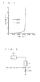
- FIG. 7 is a view showing a simulation result of the semiconductor device 100 according to Embodiment 1.
- the abscissa axis represents the elapsed time (unit: s) from the start of temperature rise of the semiconductor chip, and the ordinate axis represents the voltage (output voltage, unit: V) between both ends of the PTC element 9.
- FIG. 8 is a circuit diagram showing an example of configurations of the detection circuit.
- One end of the PTC element 9 is connected to a power supply voltage 201.
- the other end of the PTC element 9 is connected to one end of a resistance 205 at a connecting point 207.
- the other end of the resistance 205 is grounded.
- a voltage at the connecting point 207 is output as a gate voltage to the gate electrode 6 of the IGBT chip 24.
- the operation of the detection circuit is described with reference to FIG. 8.
- the resistance value of the PTC element 9 increases, and thereby the voltage at the connecting point 207 decreases to be not higher than a turn-on voltage of the semiconductor chip.
- the current stops flowing between the collector and emitter electrodes and the temperature of the IGBT chip 24 then stops rising so that thermal damage is prevented.
- the sizes of the resistance value of the resistance 205 and the power voltage 201 are set to appropriate values such that the gate voltage output from the connecting point 207 is not higher than the turn-on voltage of the IGBT chip 24 when the resistance value of the PCT element 9 increases.
- the thermal damage to the IGBT chip 24 can be more effectively prevented when the temperature rise can be detected in a shorter period of time.
- FIG. 9 is a view showing a simulation result of the relation between the film thickness of the PTC material 12 and the time for detection by the detection circuit when the PTC element 9 is used in the detection circuit.
- a line “a” indicates the time needed for detecting the temperature rise by the detection circuit after heat generation of some kind occurred for 100 ⁇ s during the steady operation of the IGBT chip 24 at 100 °C and the temperature of the IGBT chip 24 rose up to 150 °C due to the heat generation.
- the time for detection by the detection circuit is linked with the thickness of the PTC material 12 in the PTC element 9.
- a line "b" in FIG. 9 is an auxiliary straight line indicating a case where the thickness of the PTC material 12 is directly proportional to the time for detection.
- the time for detection is shortened with decrease in thickness of the PTC material 12.
- the time for detection is desirably not more than 0.5 s, which as a result requires the thickness of the PTC material 12 to be not larger than 0.37 mm.
- FIG. 9 shows the time for detection when the foregoing film thickness of the PTC material 12 is 0.1 mm.
- the IGBT chip 24 is manufactured by an ordinary production process. Subsequently, the PTC element 9 is bonded onto the IGBT chip 24. As for the place to which the PTC element 9 is bonded, since the emitter electrode 8 is often grounded and thus has a low potential, an influence exerted by the electric field on the PTC element 9 can be reduced. Therefore, the PTC element 9 is bonded onto the emitter electrode 8.
- the PTC element 9 may be damaged due to a high temperature at the time of bonding. It is thus desirable to apply a bonding means in which the temperature in bonding is not required to be high. Further, the surface of the IGBT chip 24 is usually aluminum (Al)- deposited or sputtered. Therefore, the method needs to be a bonding method capable of bonding aluminum and copper.
- FIG. 10 is a view for explaining a bonding process of the PTC element 9 by the ultrasonic and thermo-compression bonding method.
- FIG. 11 is a top view showing a conventional arrangement example on a temperature sensor 602 on the IGBT chip 24.
- a region 601 where the emitter electrode 8 of the IGBT chip 24 is present becomes a path along which a current flows and generates heat in operation of the IGBT chip 24.
- the temperature sensor 602 has hitherto been impossible to arrange the temperature sensor 602 on the region 601 where the emitter electrode 8 is present.
- the aluminum layer 410 is typically formed on the emitter electrode 8 of the IGBT chip 24 by vapor deposition. It is generally known that bonding aluminum and copper with a solder is difficult.
- the temperature sensor 602 cannot be arranged on the current path as the heat generation source, consequently, it has been required to newly provide an insulating space 603 and arrange the temperature sensor 602 on the insulating space 603.
- the ultrasonic and thermo-compression bonding method is used for bonding of the PTC element 9, it is possible to directly bond the aluminum layer 410 on the emitter electrode 8 and the copper foil electrode 11b of the PTC element 9.
- the PTC element 9 can be arranged on the region 601 where the emitter electrode 8 of the IGBT chip 24 is present. As a result, the temperature of the IGBT chip 24 can be monitored with high accuracy without upsizing the IGBT chip 24.
- the PTC element 9 has the PTC material 12 formed while being sandwiched between the copper foil electrode 11a and the copper foil electrode 11b, and the film thickness of the PTC material 12 is not smaller than 0.1 mm and not larger than 0.37 mm. This allows suppression of an error in temperature measurement and making the time for detection by the detection circuit not more than 0.5 s.
- the emitter electrode 8 is often grounded and thus has a low potential, it is possible to reduce an influence exerted by the electric field on the PTC element 9.
- the temperature does not rise, thereby enabling direct bonding between the aluminum layer 410 on the emitter electrode 8 and the copper foil electrode 11b of the PTC element 9.
- the PTC element 9 is arranged in the central part of the main surface of the IGBT chip 24. This allows detection of the maximum temperature of the semiconductor device 100 in the most accurate manner.
- the PTC element 9 is bonded through the gold bump as the conductive brazing material. It is thereby possible to increase bonding force between the PTC element 9 and the IGBT chip 24.
- the PTC element 9 includes the copper foil electrodes 11a and 11b on the whole area of its surface.
- the copper foil electrode 11a may be formed on at least part of the surface or at least part of the inside of the PTC element 9
- the copper foil electrode 11b may be formed on at least of the surface or at least part of the electrode, except for the region where the copper foil electrode 11a was formed, of the PTC element 9.
- polyethylene may be an HD (high-density) polyethylene or a LD (low-density) polyethylene.
- the conductive particles may be a metal material such as nickel, tungsten, molybdenum, cobalt, copper, silver or aluminum, or carbon black.
- polyethylene was used as the organic polymer of the PTC material 12, for example, polypropylene, polyvinylidine difluoride, polyvinyl chloride, poly vinyl acetate, ionomer, or a copolymer of these may be used.
- the IGBT chip 24 was described in present Embodiment 1, it goes without saying that this embodiment is also applicable to another semiconductor chip, such as a thyristor, a GTO (Gate Turn-Off Thyristor), a power MOSFET, a bipolar transistor, and a diode.
- a thyristor a GTO (Gate Turn-Off Thyristor)
- GTO Gate Turn-Off Thyristor
- a power MOSFET a bipolar transistor
- diode a diode
- FIG. 12 is a sectional view showing a configuration of the vicinity of the PTC element 9 of the semiconductor device 100 in accordance with the present Embodiment 2.
- Wires 20, 21 for allowing a current to flow through the PTC element 9 are connected respectively to the copper foil electrodes 11a, 11b of the PTC element 9.
- a gel (protective film) 15 is then formed so as to cover the PTC element 9.
- the PTC material 12 (see FIG. 1) includes the organic polymer. Therefore, when a transient temperature rise continues, the organic polymer melts, which might cause deformation. Further, the PTC material 12 is vulnerable to moisture, and when the PTC material 12 absorbs moisture, its physical properties may change. Further, it is desirable to avoid damage exerted by mechanical external force.
- the PTC element 9 is covered by the gel 15, for example. This enables prevention of deterioration in characteristic due to absorption of moisture from the outside and damage by external force.
- another molding member such as an epoxy resin, may be used for molding.
- the gold bump 14 was used between the copper foil electrodes 11a, 11b of the PTC element 9 and the IGBT chip 24 (see FIG. 10) in present Embodiment 1, the copper foil electrodes 11a, 11b and the surface of the IGBT chip 24 may be directly bonded to each other by the ultrasonic and thermo-compression bonding method without the use of the gold bump 14. Or an Al bump may be used in place of the gold bump 14.
- the PTC element 9 and the IGBT chip 24 are directly bonded to each other. With the gold bump 14 not used, it is possible to reduce production cost.
- bonding is performed by the ultrasonic and thermo-compression bonding method. Hence bonding is possible without a temperature rise. Bonding is possible with the surface having been aluminum-deposited or sputtered as often done on the surface of a semiconductor chip, thereby enabling an increase in bonding force.
- a low melting point solder is used for bonding between the copper foil electrodes 11a, 11b of the PTC element 9 and the IGBT chip 24 as shown in FIG. 1.
- the use of the low melting point solder with a lower melting point than that of the PTC material 12 permits prevention of damage to the PTC material 12. Further, since a thermal conductivity of the low melting point solder is relatively high, it is possible to improve performance of temperature detection.
- Examples of the low melting point solder to be used may include Anatomical Alloy, Lipowitz's Alloy, Wood Alloy, Rose Alloy, Darcet Alloy, Newton Alloy, Cerrosafe Alloy, and D Alloy. Further, the use of a flux for bonding to an aluminum surface allows bonding to the aluminum-deposited or sputtered surface.
- a conductive paste is used for bonding of the copper foil electrodes 11a, 11b of the PTC element 9 and the IGBT chip 24 as shown in FIG. 1.
- the use of the conductive paste allows bonding of the PTC element 9 at a temperature not higher than the melting point of the PTC material 12 without a temperature rise, so as to prevent damage to the PTC material 12. Further, bonding to the aluminum-deposited or sputtered surface is also possible.
- a non-organic material including BaTiO 3 as a main material is used as the PTC material 12 of the PTC element 9 as shown in FIG. 1.
- Ba is replaced by positive trivalent La, Ce, Pr, Nd, Sm, Gd, Ho or the like, or Ti is replaced by positive pentavalent Nb, Ta, Sb, Bi or the like, electrons or halls are formed to give a semiconductor.
- the temperature exceeds the Curie point, only crystal particles are insulated to increase a resistivity, thereby expressing PTC.
- the effect of using such a material as the PTC material 12 is that, since controlling the temperature at which the resistivity sharply increases is easy, such a PTC characteristic can be easily obtained that the voltage change becomes larger at 125 °C, 130 °C, 150 °C, 175 °C or another temperature.
- the material is a kind of ceramic, it is heat-resistant and hence a normal solder or a lead-free solder can be used.
- the surface of the IGBT chip 24 is typically Al-deposited or sputtered, the aluminum surface is Ni plated or Ni vapor deposited for the purpose of making aluminum and copper solder-bonded to each other, whereby copper and the aluminum surface can be solder-bonded to each other.
- Examples of the non-organic PTC material 12 other than this may include: a material made of (V 1-x Cr) 2 O 3 obtained by using V 2 O 3 as a main material and replacing part of V by Cr; a material obtained by making Bi and TiO 2 composite; a material obtained by making Bi, PbO, B 2 O 3 and SiO 2 composite; and a material obtained by making metal powder composite with ceramic and low melting point glass.
- a conductive brazing material is used for bonding between the copper foil electrodes 11a, 11b of the PTC element 9 and the semiconductor chip as shown in FIG. 1.
- the use of the conductive brazing material allows production of the semiconductor device 100 having strong bonding force and excellent thermal transfer properties.
- FIG. 13 is a sectional view showing a configuration of a semiconductor device 800 according to present Embodiment 8.
- an NTC (negative temperature coefficient) element (NTC temperature sensor) 210 is used in place of the PTC element 9.
- the NTC element 210 is a variable resistor element whose resistance value changes according to the temperature and which has a negative temperature coefficient.
- the configuration of the IGBT chip 24 portion is the same as the configuration shown in FIG. 2.
- the NTC element 210 includes; an NTC material 220 (NTC member having a negative temperature coefficient), a copper foil electrode 211a (first electrode) formed on one main surface of the NTC material 210; and a copper foil electrode 211b (second electrode) formed on the other main surface of the NTC material 220.
- NTC material 220 NTC member having a negative temperature coefficient
- the copper foil electrodes 211a (positive), 211b (negative) are bonded to both main surfaces of the NTC material 220.
- the thickness of the copper foil electrodes 211a, 211 b is from 1 to 100 mm, for example.
- the emitter electrode 8 Since the emitter electrode 8 is often grounded and thus has a low potential, an influence exerted by the electric field on the NTC element 210 can be reduced. Therefore, the copper foil electrode 211b of the NTC element 210 is bonded onto the emitter electrode 8.
- the bonding is made on the aluminum layer 410 aluminum-deposited or sputtered on the emitter electrode 8. Since a solder cannot be normally used for bonding onto the aluminum layer 410, a conductive paste, especially a silver paste having large thermal conductivity and electrical conductivity is used for the bonding. Here, an insulating layer is not provided between the NTC element 210 and the aluminum layer 410. This enables improvement in thermal transfer properties.
- the NTC material 220 is composed of Mn, Ni, or Co, or includes Mn, Ni, Co, or Fe as a main material.
- FIG. 14 is a view showing the temperature (abscissa axis) -- resistance value (ordinate axis) characteristic of the NTC element 210. It is found from FIG. 14 that the resistance value of the NTC material 220 smoothly decreases with increase in its temperature. Namely, the NTC material 220 has a negative temperature coefficient with respect to the temperature.
- the effect of using such a material is that, since the resistance value smoothly decreases with respect to the temperature, it is possible to monitor a temperature change of a semiconductor chip not only at a point of temperature but also in a large temperature range, which is different from the PTC material 12 whose resistance value sharply changes at one point as shown in FIG. 5. Further, since the resistance change with respect to the temperature change is large, the output voltage changes by dozens of mV to several mV with respect to the temperature change per 1 °C, thereby eliminating the need for a highly accurate detection circuit.
- FIG. 15 is a sectional view showing a configuration of the power semiconductor module 500 using the semiconductor device 800 according to present Embodiment 8.
- the IGBT chip 24 and the detection circuit device 300 including a detection circuit are bonded onto an insulating substrate 400 inside a case 402.
- the insulating substrate 400 is bonded onto a base board 401.
- An insulating member 403 such as a gel or a transfer mold is inserted in the case 402 for insulation.
- Terminals such as an emitter terminal 404, a collector terminal 405, and a terminal 411 are imbedded in the case 402.
- the external electrode, the IGBT chip 24 and the detection circuit device 300 are connected through a wire 406.
- FIG. 16 is an equivalent circuit diagram of the power semiconductor module 500 configured as thus described. Constituents corresponding to those of FIG. 15 are provided with the same numerals as in FIG. 15.
- the emitter electrode 8 of the IGBT chip 24 is grounded.
- the emitter of the IGBT chip 24 is connected to one end of the NTC element 210.
- the other end of the NTC element 210 is connected to one end of a resistance 208 and one input of a comparator 202 at a connecting point 209, the resistance 208 and the comparator 202 configuring the detection circuit device 300.
- the gate of the IGBT chip 24 is connected to the output of the comparator 202 configuring the detection circuit device 300.
- the other end of the resistance 208 is connected to a constant voltage power supply 221.
- the other input of the comparator 202 is connected to respective one ends of a resistance 203 and a resistance 204 at a connecting point 206.
- the other end of the resistance 203 is grounded, and the other end of the resistance 204 is connected to a constant voltage power supply 210a.
- a positive voltage is applied to the collector electrode 10, and the emitter electrode 8 is grounded.
- the positive voltage with respect to the emitter electrode 8 is applied to the gate electrode 6, an n-type channel where electrons have been gathered is formed in the p region 1 portion immediately below the polysilicon gate 5 (see FIG. 2).
- the electrons supplied from the emitter electrode 8 flow through a path leading to the p-type semiconductor substrate 4 and the collector electrode 10 via the n + layer 3, the n-type channel formed inside the p region 1 and the n' layer 2.
- holes are supplied from the p-type semiconductor substrate 4 containing a large amount of impurities to the n - layer 2 in synchronization with flowing of excess electrons into the n' layer 2. Namely, the current flows in the form of combining the electrons and the holes in the n - layer 2, and hence the device comes into a switch-on state.
- both the current and the voltage are generated between the emitter electrode 8 and the collector electrode 10, to generate Joule heat.
- the temperature For avoiding thermal damage due to the Joule heat, it is necessary to control the temperature to a temperature of not higher than 125 °C, 130 °C, 150 °C or 175 °C.
- a current is allowed to flow through the NTC element 210 and a voltage value of the NTC element 210 is read for detecting the temperature of the IGBT chip 24.
- the constant voltage power supply 221 is used as the power supply to be applied to the NTC element 210.
- current paths of a current for a sensor (measurement current) in the NTC element 210 are indicated by dotted lines.
- the current for a sensor flows to the NTC element 210 through the resistance 208.
- the current for a sensor passes through the NTC material 220 from the copper foil electrode 211 a, and then passes through the copper foil electrode 211 b to flow into the emitter electrode 8 and the aluminum layer 410 on the top of the emitter electrode 8.
- the current for a sensor then flows to the emitter terminal 404.
- the current for a sensor of the NTC element 210 flows directly through the emitter electrode 8 and the aluminum layer 410.
- a current in the main circuit passes through the IGBT chip 24 from the collector external terminal 405 and flows into the emitter terminal 404.
- the main circuit current and the current for a sensor of the NTC element 210 are mixed on the surface (the emitter electrode 8 and the aluminum layer 410) of the IGBT chip 24, which may cause noise generation.
- the resistance value of the NTC element 210 is dozens of kOhm at room temperature and hundreds of Ohm at 150 °C, having much larger impedance than the chip surface, a variation in measurement current is small and an influence exerted by noise is small.
- a voltage (reference voltage Vr) resulting from division of the constant voltage power supply 210a by the resistances 203, 204 is output at the connecting point 206.
- the voltage value at the connecting point 207 is higher than the reference voltage Vr since the resistance value of the NTC element 210 is large (see FIG. 14). Since the resistance value of the NTC element 210 decreases with increase in temperature, the voltage at the connecting point 207 falls below the reference voltage Vr.
- the comparator 202 Upon input of the voltage higher than the reference voltage Vr, the comparator 202 outputs a signal voltage to the gate of the IGBT 24. Upon input of the signal voltage, the IGBT chip 24 is turned on to allow the current to flow between the collector and the emitter.
- the comparator 202 stops outputting the gate voltage to the gate of the IGBT chip 24. Therefore, the IGBT chip 24 is turned off and the current then does not flow between the collector and emitter so that the temperature rise of the IGBT chip 24 stops to prevent thermal damage.
- FIG. 17 is a view showing a calculation result of the time for detection by the detection circuit device 300 with respect to the thickness of the NTC material 220.
- a line “a” indicates the time needed for detecting the temperature rise by the detection circuit device 300 after heat generation of some kind occurred for 100 ⁇ s during the steady operation of the IGBT chip 24 at 100 °C and the temperature of the IGBT chip 24 rose up to 150 °C due to the heat generation.
- the time for detection by the detection circuit 300 is linked with the thickness of the NTC material 220 in the NTC element 210.
- a lines "b" and “c" in FIG. 17 are auxiliary straight lines each indicating a case where the thickness of the NTC material 220 is directly proportional to the time for detection.
- the time for detection is desirably not more than 0.5 s, and it is found with reference to FIG. 17 that the time for detection can be made approximately not more than 0.5 s if the film thickness of the NTC material 220 is made not larger than 0.5 mm.
- the film thickness of the NTC material 220 is desirably not larger than 0.3 mm.
- the resistance value is proportional to the thickness of the NTC material 220
- the thickness of the NTC material 220 needs to be made uniform in order to obtain a highly accurate temperature sensor.
- the variations in resistance value of the NTC element 210 need to be kept within ⁇ 1%. It is therefore necessary to control the thickness of the NTC material 220 to be within ⁇ 1%
- the NTC material 220 is cut by machine work during the production, and fine-adjusted with polishing depending upon the circumstance.
- the thickness cannot be controlled within ⁇ 1% due to a limitation in terms of mechanical work, and thereby the individual difference becomes larger to cause deterioration in accuracy. Accordingly, the film thickness of the NTC material 220 needs to be not smaller than 0.1 mm.
- the semiconductor device 800 according to the present Embodiment 8 uses the NTC element 210. Thereby, the semiconductor device 800 has the same effect as in Embodiment 1 and is capable of monitoring the temperature of the IGBT chip 24 in a wide temperature range as compared with the PTC element 9.
- the NTC element 210 has the NTC material 220 between the copper foil electrodes 211 a, 211 b, and the film thickness of the NTC material 220 is not smaller than 0.1 mm and not larger than 0.5 mm.
- the time for detection can further be shortened by making the film thickness of the 220 not smaller than 0.1 mm and not larger than 0.3 mm.
- the detection circuit device 300 including the equivalent circuit shown in FIG. 16 was used in the semiconductor device 800 according to present Embodiment 8, a simpler detection circuit device 300 may be used as shown in FIG. 6 of Embodiment 1.
- Embodiments 2 to 5 and 7 are also applicable to present Embodiment 8.
Abstract
Description
- The present invention relates to a semiconductor device including a temperature sensor.
- In a semiconductor device as a power device which is in heavy use for power control, a temperature rises with increase in operating current. There are some cases where the semiconductor device is extremely heavily used, and in such cases, the rising temperature might exceed a threshold limit to cause multifunction of the semiconductor device or lead to damage thereto.
- Therefore, for example in an invention disclosed in
Patent Document 1, a semiconductor device is designed such that a diode temperature sensor is formed inside the semiconductor chip to monitor a temperature of a semiconductor chip, and in the case of detecting an extreme temperature rise, the operation of the semiconductor device is controlled. - Patent Document 1:
Japanese Patent Laid-Open No. 2000-031 290 - As a conventionally used temperature sensor other than this sensor, an IC temperature sensor can be cited. These temperature sensors allow a minute electric current to flow and then monitor an output voltage so as to detect a temperature. Both sensors have the characteristic of being capable of measuring a large range of temperatures, but an output voltage per 1 °C changes to a small degree and an amount of such a change is several mV.
- Therefore, detection of the amount of change requires provision of a highly accurate detection circuit capable of detecting an output voltage difference of several mV. Further, there is a problem in that, since an environment where the semiconductor device is used is a high-noise environment, the minute electric current is drowned out by the noise and the temperature cannot be sufficiently monitored.
- Moreover, although the diode temperature sensor can be directly set on the semiconductor chip, this makes variations large and causes a problem in terms of accuracy in temperature measurement.
- The IC temperature sensor is accurate in temperature measurement, but cannot be directly set on the semiconductor chip, and hence there is no choice but to measure the temperature via a heat conduction material. For this reason, heat resistance of the IC temperature sensor in the semiconductor chip becomes a problem, thereby making it difficult also for this sensor to perform accurate temperature measurement.
- Since the respective temperature sensors have the problems as thus described, it is difficult for a semiconductor device using either of such temperature sensors to accurately monitor a temperature of a semiconductor chip in a noise environment.
- An object of the present invention is to provide a semiconductor device capable of accurately monitoring a temperature of a semiconductor chip even in a noise environment, while not requiring a highly accurate detection circuit.
- An aspect of a semiconductor device according to the present invention comprises: a semiconductor chip having an emitter-side main electrode and a collector-side main electrode; and a variable resistor element, which is bonded onto the emitter-side main electrode and whose resistance value changes according to a temperature, wherein the variable resistor element includes a first electrode formed on a part of the surface or the inside of the variable resistor element at least, and a second electrode formed on a part of the surface or the inside, except for the first electrode, of the variable resistor element at least.
- According to the aspect of the semiconductor device in the present invention, since a variable resistor element is arranged on an emitter electrode as a heat generation source, the temperature of the semiconductor chip can be detected with high accuracy by detecting a change in resistance of the variable resistor element. Moreover, adoption of a variable resistor element, in which an amount of change in resistance per degree Celsius is large, eliminates the need for a highly accurate detection circuit, and allows highly accurate detection of the temperature of the semiconductor chip even in a noise environment. Furthermore, bonding of the variable resistor element onto a ground electrode leads to reduction in influence exerted by the electric field on the variable resistor element, making it possible to perform highly accurate temperature detection.
- The object, characteristics, aspects and advantages of the present invention become more apparent by the following specific descriptions and attached drawings.
-
- FIG. 1
- is a sectional view showing a configuration of a semiconductor device according to
Embodiment 1. - FIG. 2
- is an expanded sectional view showing the configuration of the semiconductor device according to
Embodiment 1. - FIG. 3
- is a top view for explaining a bonded position of a PTC element according to
Embodiment 1. - FIG. 4
- is a sectional view for explaining the bonded position of the PTC element according to
Embodiment 1. - FIG. 5
- is a view showing the temperature-resistivity characteristic of the PTC element according to
Embodiment 1. - FIG. 6
- is an equivalent circuit diagram of the semiconductor device according to
Embodiment 1. - FIG. 7
- is a view showing a simulation result of an output voltage of the PTC element according to
Embodiment 1. - FIG. 8
- is a circuit view showing an example of configurations of a detection circuit according to
Embodiment 1. - FIG. 9
- is a view showing a calculation result of the time for detection by the detection circuit with respect to the film thickness of a PTC material according to
Embodiment 1. - FIG. 10
- is a view for explaining a bonding process of the PTC element by an ultrasonic and thermo-compression bonding method.
- FIG. 11
- is a top view showing an arrangement example of a conventional temperature sensor on an IGBT chip.
- FIG. 12
- is a sectional view showing a configuration of the vicinity of a PTC element of a semiconductor device according to
Embodiment 2. - FIG. 13
- is a sectional view showing a configuration of a semiconductor device according to
Embodiment 8. - FIG. 14
- is a view showing the temperature-resistivity characteristic of an NTC element according to
Embodiment 8. - FIG. 15
- is a sectional view showing a configuration of a power semiconductor module according to
Embodiment 8. - FIG. 16
- is an equivalent circuit diagram showing the configuration of the power semiconductor chip module according to
Embodiment 8. - FIG. 17
- is a view showing the relation between the thickness of the NTC element and the time for detection according to
Embodiment 8. - FIG. 1 is a sectional view showing a configuration of a
semiconductor device 100 according topresent Embodiment 1. In thesemiconductor device 100 according topresent Embodiment 1, a PTC (positive temperature coefficient) element (PTC temperature sensor) 9 is bonded to an IGBT (insulated gate bipolar transistor)chip 24 as a kind of semiconductor chips. - A
silicon oxide film 7 is formed on the top surface of asemiconductor layer 600. A plurality ofemitter electrodes 8 are formed in thesilicon oxide film 7. - Here, the
emitter electrodes 8 are usually connected to a ground potential. - An
aluminum layer 410 for connecting the plurality ofemitter electrodes 8 is formed on theemitter electrodes 8. Here, the combination of the plurality ofemitter electrodes 8 and thealuminum layer 410 is understood as an emitter-side main electrode. - A
PTC element 9 is bonded onto thealuminum layer 410. ThePTC element 9 is a variable resistor element having a positive temperature coefficient in which a resistivity changes according to a temperature. Acollector electrode 10 is formed on the opposite side surface to the surface onto which thePTC element 9 is bonded in thesemiconductor layer 600. Here, thecollector electrode 10 is understood as a collector side main electrode. - A constant
current source 22 is connected to thePTC element 9. A voltage monitor 23 for monitoring an output voltage of thePTC element 9 is connected to thePTC element 9. - Next, the configuration of the
semiconductor device 100 shown in FIG. 1 is more specifically described by means of FIG. 2. FIG. 2 is an expanded sectional view showing the configuration of thesemiconductor device 100 in theportion 700 of FIG. 1. - An n-type semiconductor layer (n- layer) 2 having a low impurity concentration is formed on a p(p+)-
type semiconductor substrate 4 having a high impurity concentration. A p-type semiconductor region (p region) 1 is formed in a surface layer part of the n- layer 2. An n-type semiconductor region (n+ region) 3 having a high impurity concentration is formed in a surface layer part of thep region 1. - The
silicon oxide film 7 is formed on the n- layer 2. Apolysilicon gate 5 is formed inside thesilicon oxide film 7. Thepolysilicon gate 5 is formed above thep region 1 sandwiched between the n'layer 2 and the n+ region 3. Agate electrode 6 is formed on thepolysilicon gate 5. The emitter electrode (current output electrode) 8 is formed inside thesilicon oxide film 7 so as to be in contact with the n+ region 3. Thealuminum layer 410 is formed on thesilicon oxide film 7. Thecollector electrode 10 is formed on the rear surface of the p-type semiconductor substrate 4. - Next, the configuration of the
PTC element 9 is specifically described with reference to FIG. 1. ThePTC element 9 includes: a PTC material (PTC member having a positive temperature coefficient) 12; acopper foil electrode 11a (first electrode) formed on one main surface of thePTC material 12; and acopper foil electrode 11b (second electrode) formed on the other main surface of thePTC material 12. Namely, thecopper foil electrodes 11a (positive) and 11b (negative) are fusion-bonded on the respective main surfaces of thePTC material 12. The respective thicknesses of thecopper foil electrodes PTC material 12 is obtained by mixing conductive particles into an organic polymer. - Here, the
PTC material 12 is formed so as to have a thickness of not smaller than 0.1 mm and not larger than 0.37 mm. - When a voltage of not smaller than 100 V/mm is applied to the
PTC material 12, a resistance value sharply decreases in principle, thereby making the use as the temperature sensor difficult. - In many cases, the power supply connected to the
PTC element 9 is a constant voltage power supply on the order of 10 V. Therefore, when the thickness of thePTC material 12 is not larger than 0.1 mm, a voltage of not smaller than 100 V/mm is applied. It is thus necessary to make the film thickness of thePTC material 12 not smaller than 0.1 mm in order to use thePTC element 9 as the temperature sensor. - Further, as described later, when the
PTC element 9 is used as the temperature sensor, it is necessary to make the film thickness of thePTC material 12 not larger than 0.37 mm so that the time for detecting a temperature rise of the semiconductor chip is not more than 0.5 seconds. - Next, the bonding position of the
PTC element 9 is described with reference to FIGS. 3 and 4. FIG. 3 is a top view for explaining the bonding position of thePTC element 9 according topresent Embodiment 1. Further, FIG. 4 is a sectional view along the A-A line of FIG. 3. - As shown in FIGS. 3 and 4, the
PTC element 9 is arranged in the central part of theIGBT chip 24 as seen from the top. The temperature of theIGBT chip 24 is made highest in its central part. This is because heat is released in the peripheral part toward the outside thereof. For detecting the maximum temperature with the highest accuracy, it is desirable to detect the temperature in the central part of theIGBT chip 24 where the temperature is made highest, and hence thePTC element 9 is bonded to the central part of the chip. - Next described are characteristics of the
PTC element 9 having the above-described configuration with reference to FIG. 5. FIG. 5 is a view showing the temperature (abscissa axis) - resistivity (ordinate axis) characteristic of thePTC element 9. - The
PTC material 12 is an organic polymer compound including polyethylene as an organic polymer and tungsten carbide particles. It is found from FIG. 5 that thePTC material 12 has a positive temperature coefficient and its resistivity sharply rises at the boundary of 130 °C. As a result, whether the temperature is higher or lower than 130 °C can be detected by thePTC element 9. - Next, the operation of the
semiconductor device 100 according topresent Embodiment 1 is described with reference to FIGS. 1, 2 and 6. FIG. 6 is an equivalent circuit diagram of thesemiconductor device 100 configured as described above. The constituents corresponding to those of FIG. 1 are provided with the same numerals as in FIG. 1. - The
emitter electrode 8 of theIGBT chip 24 is grounded, and connected with one end of thePTC element 9. The other end of thePTC element 9 is connected to the constantcurrent source 22. The voltage between one end and the other end of thePTC element 9 is monitored by avoltage monitor 23. - A positive voltage is applied to the collector electrode 10 (see FIG. 2), and the
emitter electrode 8 is grounded. When, in this state, a positive voltage with respect to theemitter electrode 8 is applied to thegate electrode 6, an n-type channel where electrons have been gathered is formed in the p-region 1 portion immediately below thepolysilicon gate 5. - Electrons supplied from the
emitter electrode 8 flow along a path leading to the p-type semiconductor substrate 4 and thecollector electrode 10 via an n+ layer 3, the n-type channel formed inside thep region 1 and the n- layer 2. In this process, in synchronization with flowing of excess electrons into the n'layer 2, holes are supplied from the p-type semiconductor substrate 4 containing a large amount of impurities to the n'layer 2.
Namely, a current flows in the form of combining electrons with holes in the n- layer 2, and hence the device comes into a switch-on state. When the application of the voltage to thegate electrode 6 is stopped, the foregoing phenomenon does not occur, and hence the device comes into a switch-off state. - Since the current does not flow between the
emitter electrode 8 and thecollector electrode 10 in the switch-off state and the voltage becomes small between theemitter electrode 8 and thecollector electrode 10 in the switch-on state, heat generation is small.
However, in shifting from the switch-on state to the switch-off state or from the switch-off state to the switch-on state, both the current and the voltage are generated between theemitter electrode 8 and thecollector electrode 10 to generate Joule heat. For avoiding thermal damage to thesemiconductor device 100 due to the Joule heat, it is necessary to control the temperature to a temperature of not higher than 125 °C, 130 °C, 150 °C or 175 °C. - Accordingly, a current is allowed to flow through the
PTC element 9 and its voltage value is read for detecting the temperature of theIGBT chip 24. - FIG. 7 is a view showing a simulation result of the
semiconductor device 100 according toEmbodiment 1. - The abscissa axis represents the elapsed time (unit: s) from the start of temperature rise of the semiconductor chip, and the ordinate axis represents the voltage (output voltage, unit: V) between both ends of the
PTC element 9. - Here shown are changes in voltage of the
PTC element 9 in the case (solid line) of temperature rise of the semiconductor chip from 100 °C to 130 °C and the case (broken line) of the temperature rise from 100 °C to 129 °C. A current of 1 mA is allowed to flow through thePTC element 9. - As found from FIG. 7, there is almost no change in voltage of the
PTC element 9 even when the temperature rises from 100 °C to 129 °C, However, There is a change in voltage by several V when the temperature rises from 100 °C to 130 °C. Since such a voltage change occurs, a voltage change can be sufficiently detected even by a simple and inexpensive detection circuit. - FIG. 8 is a circuit diagram showing an example of configurations of the detection circuit. One end of the
PTC element 9 is connected to apower supply voltage 201. The other end of thePTC element 9 is connected to one end of aresistance 205 at a connectingpoint 207. The other end of theresistance 205 is grounded. A voltage at the connectingpoint 207 is output as a gate voltage to thegate electrode 6 of theIGBT chip 24. - Next, the operation of the detection circuit is described with reference to FIG. 8. When the temperature of the
IGBT chip 24 becomes not lower than 130 °C, the resistance value of thePTC element 9 increases, and thereby the voltage at the connectingpoint 207 decreases to be not higher than a turn-on voltage of the semiconductor chip. When the voltage becomes not higher than the turn-on voltage, the current stops flowing between the collector and emitter electrodes and the temperature of theIGBT chip 24 then stops rising so that thermal damage is prevented. - It is to be noted that the sizes of the resistance value of the
resistance 205 and thepower voltage 201 are set to appropriate values such that the gate voltage output from the connectingpoint 207 is not higher than the turn-on voltage of theIGBT chip 24 when the resistance value of thePCT element 9 increases. - In the case of detecting the temperature rise of the
IGBT chip 24 with use of the detection circuit as thus described, the thermal damage to theIGBT chip 24 can be more effectively prevented when the temperature rise can be detected in a shorter period of time. - FIG. 9 is a view showing a simulation result of the relation between the film thickness of the
PTC material 12 and the time for detection by the detection circuit when thePTC element 9 is used in the detection circuit. - A line "a" indicates the time needed for detecting the temperature rise by the detection circuit after heat generation of some kind occurred for 100 µs during the steady operation of the
IGBT chip 24 at 100 °C and the temperature of theIGBT chip 24 rose up to 150 °C due to the heat generation. As shown in FIG. 9, the time for detection by the detection circuit is linked with the thickness of thePTC material 12 in thePTC element 9. - Further, a line "b" in FIG. 9 is an auxiliary straight line indicating a case where the thickness of the
PTC material 12 is directly proportional to the time for detection. - As shown in FIG. 9, it is found that the time for detection is shortened with decrease in thickness of the
PTC material 12. In actual application, the time for detection is desirably not more than 0.5 s, which as a result requires the thickness of thePTC material 12 to be not larger than 0.37 mm. - Here, FIG. 9 shows the time for detection when the foregoing film thickness of the
PTC material 12 is 0.1 mm. - Next described is a method for manufacturing the
semiconductor device 100 according topresent Embodiment 1. - First, the
IGBT chip 24 is manufactured by an ordinary production process. Subsequently, thePTC element 9 is bonded onto theIGBT chip 24. As for the place to which thePTC element 9 is bonded, since theemitter electrode 8 is often grounded and thus has a low potential, an influence exerted by the electric field on thePTC element 9 can be reduced. Therefore, thePTC element 9 is bonded onto theemitter electrode 8. - If a normal solder is used in bonding, the
PTC element 9 may be damaged due to a high temperature at the time of bonding. It is thus desirable to apply a bonding means in which the temperature in bonding is not required to be high. Further, the surface of theIGBT chip 24 is usually aluminum (Al)- deposited or sputtered. Therefore, the method needs to be a bonding method capable of bonding aluminum and copper. - Accordingly, an ultrasonic and thermo-compression bonding method shown in FIG. 10 is used. FIG. 10 is a view for explaining a bonding process of the
PTC element 9 by the ultrasonic and thermo-compression bonding method. - This is a method in which a gold bump (conductive brazing material) 14 is sandwiched between the
copper foil electrode 11b of thePTC element 9 and the surface of theIGBT chip 24, i.e. the surface of thealuminum layer 410 on theemitter electrode 8 inpresent Embodiment 1, and supersonic vibration is applied to thePTC element 9 or theIGBT chip 24 through anvibration exciter 13, and in which bonding can be performed while there is almost no temperature rise. Further, in the present bonding method, it is possible to bond aluminum and copper. - In the following, the effect of the
semiconductor device 100 according topresent Embodiment 1 is described. FIG. 11 is a top view showing a conventional arrangement example on atemperature sensor 602 on theIGBT chip 24. Aregion 601 where theemitter electrode 8 of theIGBT chip 24 is present becomes a path along which a current flows and generates heat in operation of theIGBT chip 24. - It has hitherto been impossible to arrange the
temperature sensor 602 on theregion 601 where theemitter electrode 8 is present. Namely, thealuminum layer 410 is typically formed on theemitter electrode 8 of theIGBT chip 24 by vapor deposition. It is generally known that bonding aluminum and copper with a solder is difficult. - Since the
temperature sensor 602 cannot be arranged on the current path as the heat generation source, consequently, it has been required to newly provide aninsulating space 603 and arrange thetemperature sensor 602 on the insulatingspace 603. - This has required expansion of the
region 601 by the size of the insulatingspace 603, causing a problem of upsizing theIGBT chip 24. Further, since thetemperature sensor 602 is separated from the top of the current path as the heat generation source, it has been difficult to detect the maximum temperature of theIGBT chip 24. - In the
semiconductor device 100 according topresent Embodiment 1, since the ultrasonic and thermo-compression bonding method is used for bonding of thePTC element 9, it is possible to directly bond thealuminum layer 410 on theemitter electrode 8 and thecopper foil electrode 11b of thePTC element 9. - Therefore, in the
semiconductor device 100 according topresent Embodiment 1, thePTC element 9 can be arranged on theregion 601 where theemitter electrode 8 of theIGBT chip 24 is present. As a result, the temperature of theIGBT chip 24 can be monitored with high accuracy without upsizing theIGBT chip 24. - Further, since a change in output voltage per 1 °C is large in the
PTC element 9, a highly accurate detection circuit is not necessary, thereby allowing accurate monitoring of the temperature of theIGBT chip 24 even in a noise environment. - The
PTC element 9 has thePTC material 12 formed while being sandwiched between thecopper foil electrode 11a and thecopper foil electrode 11b, and the film thickness of thePTC material 12 is not smaller than 0.1 mm and not larger than 0.37 mm. This allows suppression of an error in temperature measurement and making the time for detection by the detection circuit not more than 0.5 s. - Further, since the
emitter electrode 8 is often grounded and thus has a low potential, it is possible to reduce an influence exerted by the electric field on thePTC element 9. - In the
semiconductor device 100 according topresent Embodiment 1, since thePTC element 9 is bonded by the ultrasonic and thermo-compression bonding method, the temperature does not rise, thereby enabling direct bonding between thealuminum layer 410 on theemitter electrode 8 and thecopper foil electrode 11b of thePTC element 9. - As a result, it is possible to directly bond
PTC element 9 and the p-type semiconductor substrate 4 in no danger of damage due to application of heat at a high temperature. - In the
semiconductor device 100 according topresent Embodiment 1, thePTC element 9 is arranged in the central part of the main surface of theIGBT chip 24. This allows detection of the maximum temperature of thesemiconductor device 100 in the most accurate manner. - In the
semiconductor device 100 according topresent Embodiment 1, thePTC element 9 is bonded through the gold bump as the conductive brazing material. It is thereby possible to increase bonding force between thePTC element 9 and theIGBT chip 24. - It is to be noted that as shown in FIG. 1, the
PTC element 9 includes thecopper foil electrodes copper foil electrode 11a may be formed on at least part of the surface or at least part of the inside of thePTC element 9, and thecopper foil electrode 11b may be formed on at least of the surface or at least part of the electrode, except for the region where thecopper foil electrode 11a was formed, of thePTC element 9. Even with such a configuration, the temperature of theIGBT chip 24 can be monitored with high accuracy by allowing a constant current to flow through thePTC material 12 sandwiched between thecopper foil electrodes - Further, although the case was described in
present Embodiment 1 where the resistance of thePTC material 12 increases at a temperature of 130 °C, detection can also be performed at another temperature, such as 125 °C, 150 °C or 175 °C, by changing the melting point of the organic polymer. Further, polyethylene may be an HD (high-density) polyethylene or a LD (low-density) polyethylene. - Moreover, although tungsten carbide was used as the conductive particles of the
PTC material 12 inpresent Embodiment 1, the conductive particles may be a metal material such as nickel, tungsten, molybdenum, cobalt, copper, silver or aluminum, or carbon black. - Furthermore, although polyethylene was used as the organic polymer of the
PTC material 12, for example, polypropylene, polyvinylidine difluoride, polyvinyl chloride, poly vinyl acetate, ionomer, or a copolymer of these may be used. - Although the
IGBT chip 24 was described inpresent Embodiment 1, it goes without saying that this embodiment is also applicable to another semiconductor chip, such as a thyristor, a GTO (Gate Turn-Off Thyristor), a power MOSFET, a bipolar transistor, and a diode. - FIG. 12 is a sectional view showing a configuration of the vicinity of the
PTC element 9 of thesemiconductor device 100 in accordance with thepresent Embodiment 2. -
Wires PTC element 9 are connected respectively to thecopper foil electrodes PTC element 9. A gel (protective film) 15 is then formed so as to cover thePTC element 9. - The PTC material 12 (see FIG. 1) includes the organic polymer. Therefore, when a transient temperature rise continues, the organic polymer melts, which might cause deformation. Further, the
PTC material 12 is vulnerable to moisture, and when thePTC material 12 absorbs moisture, its physical properties may change. Further, it is desirable to avoid damage exerted by mechanical external force. - In
present Embodiment 2, as shown in FIG. 12, thePTC element 9 is covered by thegel 15, for example. This enables prevention of deterioration in characteristic due to absorption of moisture from the outside and damage by external force. - It is to be noted that, other than covering by the
gel 15, another molding member, such as an epoxy resin, may be used for molding. - Although the
gold bump 14 was used between thecopper foil electrodes PTC element 9 and the IGBT chip 24 (see FIG. 10) inpresent Embodiment 1, thecopper foil electrodes IGBT chip 24 may be directly bonded to each other by the ultrasonic and thermo-compression bonding method without the use of thegold bump 14. Or an Al bump may be used in place of thegold bump 14. - In
present Embodiment 3, thePTC element 9 and theIGBT chip 24 are directly bonded to each other. With thegold bump 14 not used, it is possible to reduce production cost. - In
present Embodiment 3, bonding is performed by the ultrasonic and thermo-compression bonding method. Hence bonding is possible without a temperature rise. Bonding is possible with the surface having been aluminum-deposited or sputtered as often done on the surface of a semiconductor chip, thereby enabling an increase in bonding force. - In the
semiconductor device 100 according topresent Embodiment 4, a low melting point solder is used for bonding between thecopper foil electrodes PTC element 9 and theIGBT chip 24 as shown in FIG. 1. - The use of the low melting point solder with a lower melting point than that of the
PTC material 12 permits prevention of damage to thePTC material 12. Further, since a thermal conductivity of the low melting point solder is relatively high, it is possible to improve performance of temperature detection. - Examples of the low melting point solder to be used may include Anatomical Alloy, Lipowitz's Alloy, Wood Alloy, Rose Alloy, Darcet Alloy, Newton Alloy, Cerrosafe Alloy, and D Alloy. Further, the use of a flux for bonding to an aluminum surface allows bonding to the aluminum-deposited or sputtered surface.
- In the
semiconductor device 100 according topresent Embodiment 5, a conductive paste is used for bonding of thecopper foil electrodes PTC element 9 and theIGBT chip 24 as shown in FIG. 1. - The use of the conductive paste allows bonding of the
PTC element 9 at a temperature not higher than the melting point of thePTC material 12 without a temperature rise, so as to prevent damage to thePTC material 12. Further, bonding to the aluminum-deposited or sputtered surface is also possible. - In the
semiconductor device 100 according topresent Embodiment 6, a non-organic material including BaTiO3 as a main material is used as thePTC material 12 of thePTC element 9 as shown in FIG. 1. When Ba is replaced by positive trivalent La, Ce, Pr, Nd, Sm, Gd, Ho or the like, or Ti is replaced by positive pentavalent Nb, Ta, Sb, Bi or the like, electrons or halls are formed to give a semiconductor. When the temperature exceeds the Curie point, only crystal particles are insulated to increase a resistivity, thereby expressing PTC.
As a method for controlling the temperature at which the resistivity sharply increases, there is a method where Ba is replaced by positive divalent Mg, Ca, Sr, Pb or the like, or Ti is replaced by positive tetravalent Hf, Sn, Zr or the like, to shift the Curie point so that the PTC characteristic according thereto can be obtained. - The effect of using such a material as the
PTC material 12 is that, since controlling the temperature at which the resistivity sharply increases is easy, such a PTC characteristic can be easily obtained that the voltage change becomes larger at 125 °C, 130 °C, 150 °C, 175 °C or another temperature. - Further, since the material is a kind of ceramic, it is heat-resistant and hence a normal solder or a lead-free solder can be used. Since the surface of the
IGBT chip 24 is typically Al-deposited or sputtered, the aluminum surface is Ni plated or Ni vapor deposited for the purpose of making aluminum and copper solder-bonded to each other, whereby copper and the aluminum surface can be solder-bonded to each other. - Examples of the
non-organic PTC material 12 other than this may include: a material made of (V1-xCr)2O3 obtained by using V2O3 as a main material and replacing part of V by Cr; a material obtained by making Bi and TiO2 composite; a material obtained by making Bi, PbO, B2O3 and SiO2 composite; and a material obtained by making metal powder composite with ceramic and low melting point glass. - In the
semiconductor device 100 according topresent Embodiment 7, a conductive brazing material is used for bonding between thecopper foil electrodes PTC element 9 and the semiconductor chip as shown in FIG. 1. - The use of the conductive brazing material allows production of the
semiconductor device 100 having strong bonding force and excellent thermal transfer properties. - FIG. 13 is a sectional view showing a configuration of a
semiconductor device 800 according topresent Embodiment 8. In thesemiconductor device 800 according topresent Embodiment 8, an NTC (negative temperature coefficient) element (NTC temperature sensor) 210 is used in place of thePTC element 9. TheNTC element 210 is a variable resistor element whose resistance value changes according to the temperature and which has a negative temperature coefficient. Further, the configuration of theIGBT chip 24 portion is the same as the configuration shown in FIG. 2. - Other constituents are the same as those of the
semiconductor device 100 according toEmbodiment 1, and the identical constituents are provided with the identical symbols as inEmbodiment 1 so as to omit repeated description. - Next, the configuration of the
NTC element 210 is specifically described with reference to FIG. 13.
TheNTC element 210 includes; an NTC material 220 (NTC member having a negative temperature coefficient), acopper foil electrode 211a (first electrode) formed on one main surface of theNTC material 210; and a copper foil electrode 211b (second electrode) formed on the other main surface of the NTC material 220. Namely, thecopper foil electrodes 211a (positive), 211b (negative) are bonded to both main surfaces of the NTC material 220. The thickness of thecopper foil electrodes 211a, 211 b is from 1 to 100 mm, for example. - Since the
emitter electrode 8 is often grounded and thus has a low potential, an influence exerted by the electric field on theNTC element 210 can be reduced. Therefore, the copper foil electrode 211b of theNTC element 210 is bonded onto theemitter electrode 8. - More specifically, the bonding is made on the
aluminum layer 410 aluminum-deposited or sputtered on theemitter electrode 8. Since a solder cannot be normally used for bonding onto thealuminum layer 410, a conductive paste, especially a silver paste having large thermal conductivity and electrical conductivity is used for the bonding. Here, an insulating layer is not provided between theNTC element 210 and thealuminum layer 410.
This enables improvement in thermal transfer properties. Further, the NTC material 220 is composed of Mn, Ni, or Co, or includes Mn, Ni, Co, or Fe as a main material. - It is to be noted that the arrangement position of the
NTC element 210 on theIGBT chip 24 and the like are the same as those in Embodiment 1 (see FIGS. 3 and 4). - FIG. 14 is a view showing the temperature (abscissa axis) -- resistance value (ordinate axis) characteristic of the
NTC element 210. It is found from FIG. 14 that the resistance value of the NTC material 220 smoothly decreases with increase in its temperature. Namely, the NTC material 220 has a negative temperature coefficient with respect to the temperature. - The effect of using such a material is that, since the resistance value smoothly decreases with respect to the temperature, it is possible to monitor a temperature change of a semiconductor chip not only at a point of temperature but also in a large temperature range, which is different from the
PTC material 12 whose resistance value sharply changes at one point as shown in FIG. 5. Further, since the resistance change with respect to the temperature change is large, the output voltage changes by dozens of mV to several mV with respect to the temperature change per 1 °C, thereby eliminating the need for a highly accurate detection circuit. - Next, a
power semiconductor module 500 as an example of a configuration of thesemiconductor device 800 including theNTC element 210 and adetection circuit device 300 that detects the output of theNTC element 210 are described with reference to FIG. 15. FIG. 15 is a sectional view showing a configuration of thepower semiconductor module 500 using thesemiconductor device 800 according topresent Embodiment 8. - The
IGBT chip 24 and thedetection circuit device 300 including a detection circuit are bonded onto an insulatingsubstrate 400 inside acase 402. The insulatingsubstrate 400 is bonded onto abase board 401. An insulatingmember 403 such as a gel or a transfer mold is inserted in thecase 402 for insulation. - Terminals such as an
emitter terminal 404, acollector terminal 405, and a terminal 411 are imbedded in thecase 402. The external electrode, theIGBT chip 24 and thedetection circuit device 300 are connected through awire 406. - It should be noted that the configuration shown in FIG. 15 is also applicable to
Embodiment 1. - FIG. 16 is an equivalent circuit diagram of the
power semiconductor module 500 configured as thus described. Constituents corresponding to those of FIG. 15 are provided with the same numerals as in FIG. 15. - The
emitter electrode 8 of theIGBT chip 24 is grounded. The emitter of theIGBT chip 24 is connected to one end of theNTC element 210. The other end of theNTC element 210 is connected to one end of aresistance 208 and one input of acomparator 202 at a connectingpoint 209, theresistance 208 and thecomparator 202 configuring thedetection circuit device 300. - The gate of the
IGBT chip 24 is connected to the output of thecomparator 202 configuring thedetection circuit device 300. - Next, the circuit configuration of the
detection circuit device 300 is specifically described. The other end of theresistance 208 is connected to a constantvoltage power supply 221. The other input of thecomparator 202 is connected to respective one ends of aresistance 203 and aresistance 204 at a connectingpoint 206. The other end of theresistance 203 is grounded, and the other end of theresistance 204 is connected to a constantvoltage power supply 210a. - Next, the operation of the
power semiconductor module 500 is described with reference to FIGS. 2,15 and 16.
First, a positive voltage is applied to thecollector electrode 10, and theemitter electrode 8 is grounded. When, in that state, the positive voltage with respect to theemitter electrode 8 is applied to thegate electrode 6, an n-type channel where electrons have been gathered is formed in thep region 1 portion immediately below the polysilicon gate 5 (see FIG. 2). - The electrons supplied from the
emitter electrode 8 flow through a path leading to the p-type semiconductor substrate 4 and thecollector electrode 10 via the n+ layer 3, the n-type channel formed inside thep region 1 and the n'layer 2. In this process, holes are supplied from the p-type semiconductor substrate 4 containing a large amount of impurities to the n- layer 2 in synchronization with flowing of excess electrons into the n'layer 2. Namely, the current flows in the form of combining the electrons and the holes in the n- layer 2, and hence the device comes into a switch-on state. - When the application of the voltage to the
gate electrode 6 is stopped, the foregoing phenomenon does not occur, and hence the device comes into a switch-off state. - Since the current does not flow between the
emitter electrode 8 and thecollector electrode 10 in the switch-off state and the voltage becomes smaller between theemitter electrode 8 and thecollector electrode 10 in the switch-on state, heat generation is small. - However, in shifting from the switch-on state to the switch-off state or from the switch-off state to the switch-on state, both the current and the voltage are generated between the
emitter electrode 8 and thecollector electrode 10, to generate Joule heat. - For avoiding thermal damage due to the Joule heat, it is necessary to control the temperature to a temperature of not higher than 125 °C, 130 °C, 150 °C or 175 °C.
- Accordingly, a current is allowed to flow through the
NTC element 210 and a voltage value of theNTC element 210 is read for detecting the temperature of theIGBT chip 24. - In the
power semiconductor module 500 according topresent Embodiment 8, the constantvoltage power supply 221 is used as the power supply to be applied to theNTC element 210. In FIG. 15, current paths of a current for a sensor (measurement current) in theNTC element 210 are indicated by dotted lines. - When the constant
voltage power supply 221 is connected to theNTC element 210, the current for a sensor flows to theNTC element 210 through theresistance 208. The current for a sensor passes through the NTC material 220 from thecopper foil electrode 211 a, and then passes through the copper foil electrode 211 b to flow into theemitter electrode 8 and thealuminum layer 410 on the top of theemitter electrode 8. The current for a sensor then flows to theemitter terminal 404. - Since an insulating layer is not provided between the
NTC element 210 and thealuminum layer 410, the current for a sensor of theNTC element 210 flows directly through theemitter electrode 8 and thealuminum layer 410. - Meanwhile, a current in the main circuit (main circuit current) passes through the
IGBT chip 24 from the collectorexternal terminal 405 and flows into theemitter terminal 404. - Therefore, the main circuit current and the current for a sensor of the
NTC element 210 are mixed on the surface (theemitter electrode 8 and the aluminum layer 410) of theIGBT chip 24, which may cause noise generation. - However, since the resistance value of the
NTC element 210 is dozens of kOhm at room temperature and hundreds of Ohm at 150 °C, having much larger impedance than the chip surface, a variation in measurement current is small and an influence exerted by noise is small. - With reference to FIG. 16, a voltage (reference voltage Vr) resulting from division of the constant
voltage power supply 210a by theresistances point 206. - When the temperature of the
IGBT chip 24 is low, the voltage value at the connectingpoint 207 is higher than the reference voltage Vr since the resistance value of theNTC element 210 is large (see FIG. 14). Since the resistance value of theNTC element 210 decreases with increase in temperature, the voltage at the connectingpoint 207 falls below the reference voltage Vr. - Upon input of the voltage higher than the reference voltage Vr, the
comparator 202 outputs a signal voltage to the gate of theIGBT 24. Upon input of the signal voltage, theIGBT chip 24 is turned on to allow the current to flow between the collector and the emitter. - When the temperature of the
IGBT chip 24 increases and the resistance value of theNTC element 210 falls below a certain resistance value, the voltage at the connectingpoint 209 falls below the reference voltage Vr at the connectingpoint 206, and thus thecomparator 202 stops outputting the gate voltage to the gate of theIGBT chip 24. Therefore, theIGBT chip 24 is turned off and the current then does not flow between the collector and emitter so that the temperature rise of theIGBT chip 24 stops to prevent thermal damage. - It should be noted that, although the above-described relation may not be established depending upon the magnitude relation between the output voltage values of the constant
voltage power supplies voltage power supplies - The shorter the time for detecting the
NTC element 210 to be used, the more effective for preventing damage to the chip. FIG. 17 is a view showing a calculation result of the time for detection by thedetection circuit device 300 with respect to the thickness of the NTC material 220. A line "a" indicates the time needed for detecting the temperature rise by thedetection circuit device 300 after heat generation of some kind occurred for 100 µs during the steady operation of theIGBT chip 24 at 100 °C and the temperature of theIGBT chip 24 rose up to 150 °C due to the heat generation. - As shown in FIG. 17, the time for detection by the
detection circuit 300 is linked with the thickness of the NTC material 220 in theNTC element 210. - As shown in FIG. 17, it is found that the time for detection is shortened with decrease in thickness of the NTC material 220. Further, a lines "b" and "c" in FIG. 17 are auxiliary straight lines each indicating a case where the thickness of the NTC material 220 is directly proportional to the time for detection.
- In actual application, the time for detection is desirably not more than 0.5 s, and it is found with reference to FIG. 17 that the time for detection can be made approximately not more than 0.5 s if the film thickness of the NTC material 220 is made not larger than 0.5 mm.
- Moreover, it is found with reference to FIG. 17 that the time for detection sharply increases, departing from the proportional relation, when the thickness of the NTC material 220 exceeds 0.3 mm. Therefore, the film thickness of the NTC material 220 is desirably not larger than 0.3 mm.
- Further, since the resistance value is proportional to the thickness of the NTC material 220, the thickness of the NTC material 220 needs to be made uniform in order to obtain a highly accurate temperature sensor. In order to suppress an error in the temperature measurement due to individual difference of the
NTC element 210 within ±2%, the variations in resistance value of theNTC element 210 need to be kept within ±1%. It is therefore necessary to control the thickness of the NTC material 220 to be within ±1% - The NTC material 220 is cut by machine work during the production, and fine-adjusted with polishing depending upon the circumstance. The thickness cannot be controlled within ±1% due to a limitation in terms of mechanical work, and thereby the individual difference becomes larger to cause deterioration in accuracy. Accordingly, the film thickness of the NTC material 220 needs to be not smaller than 0.1 mm.
- The
semiconductor device 800 according to thepresent Embodiment 8 uses theNTC element 210. Thereby, thesemiconductor device 800 has the same effect as inEmbodiment 1 and is capable of monitoring the temperature of theIGBT chip 24 in a wide temperature range as compared with thePTC element 9. - Further, the
NTC element 210 has the NTC material 220 between thecopper foil electrodes 211 a, 211 b, and the film thickness of the NTC material 220 is not smaller than 0.1 mm and not larger than 0.5 mm. - This allows the time for detection by the
detection circuit device 300 to be not more than 0. 5 s. - Further, the time for detection can further be shortened by making the film thickness of the 220 not smaller than 0.1 mm and not larger than 0.3 mm.
- It is to be noted that, although the
detection circuit device 300 including the equivalent circuit shown in FIG. 16 was used in thesemiconductor device 800 according topresent Embodiment 8, a simplerdetection circuit device 300 may be used as shown in FIG. 6 ofEmbodiment 1. - Further, the configurations described in
Embodiments 2 to 5 and 7 are also applicable to presentEmbodiment 8.
Claims (13)
- A semiconductor device, comprising:a semiconductor chip (24) having an emitter-side main electrode (8, 410) and a collector-side main electrode (10); anda variable resistor element (9; 210), which is bonded onto the emitter-side main electrode (8, 410) and whose resistance value changes according to a temperature, whereinthe variable resistor element (9; 210) includesa first electrode (11a; 211 a) formed on a part of the surface or the inside of the variable resistor element (9; 210) at least, anda second electrode (11b; 211b) formed on a part of the surface or the inside, except for the first electrode, of the variable resistor element at least.
- The semiconductor device according to claim 1,
wherein the variable resistor element (9; 210) is bonded by an ultrasonic and thermo-compression bonding method. - The semiconductor device according to claim 1,
wherein the variable resistor element (9; 210) is bonded with a conductive brazing material. - The semiconductor device according to claim 1,
wherein the variable resistor element (9; 210) is bonded with a low melting point solder having a lower melting point than a melting point at which the variable resistor element (9; 210) melts. - The semiconductor device according to claim 1,
wherein the variable resistor element (9; 210) is bonded with a conductive paste. - The semiconductor device according to claim 1,
wherein the variable resistor element (9; 210) is solder-bonded to the semiconductor chip via (24) a Ni-surface formed on the surface of the semiconductor chip (24). - The semiconductor device according to claim 1,
further comprising a protective film (15) formed so as to cover the variable resistor element (9; 210). - The semiconductor device according to claim 1,
wherein the variable resistor element (9; 210) is arranged in the central part of the main surface of the semiconductor chip (24). - The semiconductor device according to any one of claims 1 to 8,
wherein the variable resistor element is an element (9) having a positive temperature coefficient. - The semiconductor device according to claim 9, wherein
the variable resistor (9) element further includes a variable resistor material (12) formed while being sandwiched between the first electrode (11a) and the second electrode (11b), and
the variable resistor material (12) has a film thickness of not smaller than 0.1 mm and not larger than 0.37 mm. - The semiconductor device according to any one of claims 1 to 8,
wherein the variable resistor element (210) is an element having a negative temperature coefficient. - The semiconductor device according to claim 11, wherein
the variable resistor element (210) further includes a variable resistor material (220) formed while being sandwiched between the first electrode (211a) and the second electrode (211b), and
the variable resistor material (220) has a film thickness of not smaller than 0.1 mm and not larger than 0.5 mm. - The semiconductor device according to claim 12,
wherein the variable resistor material (220) has a film thickness of not smaller than 0.1 mm and not larger than 0.3 mm.
Applications Claiming Priority (2)
| Application Number | Priority Date | Filing Date | Title |
|---|---|---|---|
| JP2004371133 | 2004-12-22 | ||
| PCT/JP2005/023253 WO2006068082A1 (en) | 2004-12-22 | 2005-12-19 | Semiconductor device |
Publications (3)
| Publication Number | Publication Date |
|---|---|
| EP1830405A1 true EP1830405A1 (en) | 2007-09-05 |
| EP1830405A4 EP1830405A4 (en) | 2011-03-30 |
| EP1830405B1 EP1830405B1 (en) | 2021-01-20 |
Family
ID=36601682
Family Applications (1)
| Application Number | Title | Priority Date | Filing Date |
|---|---|---|---|
| EP05816412.0A Active EP1830405B1 (en) | 2004-12-22 | 2005-12-19 | Semiconductor device comprising a semiconductor chip and a variable resistor element |
Country Status (4)
| Country | Link |
|---|---|
| US (1) | US7554173B2 (en) |
| EP (1) | EP1830405B1 (en) |
| JP (1) | JP4745251B2 (en) |
| WO (1) | WO2006068082A1 (en) |
Cited By (2)
| Publication number | Priority date | Publication date | Assignee | Title |
|---|---|---|---|---|
| US8478559B2 (en) | 2008-07-07 | 2013-07-02 | Infineon Technologies Ag | Semiconductor component and method of making the same |
| EP3608644A1 (en) * | 2018-08-09 | 2020-02-12 | Infineon Technologies AG | Power semiconductor circuit and method for determination of a temperature of a power semiconductor circuit |
Families Citing this family (8)
| Publication number | Priority date | Publication date | Assignee | Title |
|---|---|---|---|---|
| CN103896207B (en) * | 2014-04-14 | 2015-11-18 | 河南省科学院应用物理研究所有限公司 | A kind of carbon nano pipe array bonding method based on power electro thermal coupling |
| DE102014116759A1 (en) * | 2014-11-17 | 2016-05-19 | Infineon Technologies Austria Ag | SEMICONDUCTOR DEVICE WITH STRUCTURE WITH POSITIVE TEMPERATURE COEFFICIENT |
| DE102015112919B4 (en) * | 2015-08-06 | 2019-12-24 | Infineon Technologies Ag | Semiconductor components, a semiconductor diode and a method for forming a semiconductor component |
| CN105405818A (en) * | 2015-11-02 | 2016-03-16 | 上海晶亮电子科技有限公司 | Power module |
| JP6652003B2 (en) | 2016-07-04 | 2020-02-19 | 株式会社デンソー | Semiconductor chip and semiconductor device |
| JP6675991B2 (en) * | 2017-01-16 | 2020-04-08 | 株式会社豊田中央研究所 | Semiconductor device |
| JP2019169579A (en) * | 2018-03-23 | 2019-10-03 | 株式会社東芝 | Semiconductor device and method of manufacturing the same |
| CN116504823B (en) * | 2023-06-28 | 2023-11-07 | 湖南大学 | IGBT chip and IGBT cell integrating temperature measuring unit and method |
Citations (7)
| Publication number | Priority date | Publication date | Assignee | Title |
|---|---|---|---|---|
| US3708720A (en) * | 1973-01-02 | 1973-01-02 | Franklin Electric Co Inc | Semiconductor thermal protection |
| EP0350015A2 (en) * | 1988-07-08 | 1990-01-10 | Siemens Aktiengesellschaft | Power MOSFET with a temperature sensor |
| JPH09163592A (en) * | 1995-12-05 | 1997-06-20 | Harness Sogo Gijutsu Kenkyusho:Kk | Switching member with protective function and control circuit unit employing it |
| US5763929A (en) * | 1994-03-18 | 1998-06-09 | Kabushiki Kaisha Tokai Rika Denki Seisakusho | Transistor package having a series connected thermistor for protection from thermal destruction |
| DE19821834A1 (en) * | 1998-05-15 | 1999-11-25 | Fahrzeugklimaregelung Gmbh | Power MOS transistor (PMT) with integral overheat protection |
| US20030234245A1 (en) * | 2002-06-19 | 2003-12-25 | Cogan Adrian I. | Multiple load protection and control device |
| WO2005104743A2 (en) * | 2004-04-26 | 2005-11-10 | Rowan Electric, Inc. | Adaptive gate drive for switching devices of inverter |
Family Cites Families (12)
| Publication number | Priority date | Publication date | Assignee | Title |
|---|---|---|---|---|
| JP3008900B2 (en) * | 1985-11-29 | 2000-02-14 | 株式会社デンソー | Semiconductor device |
| JPH0693485B2 (en) * | 1985-11-29 | 1994-11-16 | 日本電装株式会社 | Semiconductor device |
| JP3308983B2 (en) | 1991-03-18 | 2002-07-29 | 東燃ゼネラル石油株式会社 | Terminally modified polyolefin |
| JP2833610B2 (en) * | 1991-10-01 | 1998-12-09 | 株式会社デンソー | Insulated gate bipolar transistor |
| JPH0677397A (en) | 1992-08-28 | 1994-03-18 | Toshiba Corp | Detecting device for temperature abnormality of semiconductor |
| US5883402A (en) * | 1995-11-06 | 1999-03-16 | Kabushiki Kaisha Toshiba | Semiconductor device and protection method |
| JPH10125620A (en) * | 1996-10-17 | 1998-05-15 | Denso Corp | Silicon carbide semiconductor device |
| JP2000031290A (en) | 1998-07-10 | 2000-01-28 | Nissan Motor Co Ltd | Semiconductor device |
| JP2000338146A (en) * | 1999-05-26 | 2000-12-08 | Matsushita Electric Works Ltd | Current detecting circuit |
| JP2001025159A (en) * | 1999-07-02 | 2001-01-26 | Murata Mfg Co Ltd | Protection circuit |
| JP2004063606A (en) * | 2002-07-26 | 2004-02-26 | Matsushita Electric Works Ltd | Overcurrent protection device |
| JP2005039948A (en) | 2003-07-16 | 2005-02-10 | Sharp Corp | Semiconductor device and electronic apparatus |
-
2005
- 2005-12-19 US US11/722,112 patent/US7554173B2/en active Active
- 2005-12-19 WO PCT/JP2005/023253 patent/WO2006068082A1/en active Application Filing
- 2005-12-19 JP JP2006548967A patent/JP4745251B2/en active Active
- 2005-12-19 EP EP05816412.0A patent/EP1830405B1/en active Active
Patent Citations (7)
| Publication number | Priority date | Publication date | Assignee | Title |
|---|---|---|---|---|
| US3708720A (en) * | 1973-01-02 | 1973-01-02 | Franklin Electric Co Inc | Semiconductor thermal protection |
| EP0350015A2 (en) * | 1988-07-08 | 1990-01-10 | Siemens Aktiengesellschaft | Power MOSFET with a temperature sensor |
| US5763929A (en) * | 1994-03-18 | 1998-06-09 | Kabushiki Kaisha Tokai Rika Denki Seisakusho | Transistor package having a series connected thermistor for protection from thermal destruction |
| JPH09163592A (en) * | 1995-12-05 | 1997-06-20 | Harness Sogo Gijutsu Kenkyusho:Kk | Switching member with protective function and control circuit unit employing it |
| DE19821834A1 (en) * | 1998-05-15 | 1999-11-25 | Fahrzeugklimaregelung Gmbh | Power MOS transistor (PMT) with integral overheat protection |
| US20030234245A1 (en) * | 2002-06-19 | 2003-12-25 | Cogan Adrian I. | Multiple load protection and control device |
| WO2005104743A2 (en) * | 2004-04-26 | 2005-11-10 | Rowan Electric, Inc. | Adaptive gate drive for switching devices of inverter |
Non-Patent Citations (1)
| Title |
|---|
| See also references of WO2006068082A1 * |
Cited By (3)
| Publication number | Priority date | Publication date | Assignee | Title |
|---|---|---|---|---|
| US8478559B2 (en) | 2008-07-07 | 2013-07-02 | Infineon Technologies Ag | Semiconductor component and method of making the same |
| DE102009027487B4 (en) * | 2008-07-07 | 2020-02-27 | Infineon Technologies Ag | Determination of the temperature of a semiconductor component |
| EP3608644A1 (en) * | 2018-08-09 | 2020-02-12 | Infineon Technologies AG | Power semiconductor circuit and method for determination of a temperature of a power semiconductor circuit |
Also Published As
| Publication number | Publication date |
|---|---|
| WO2006068082A9 (en) | 2006-10-19 |
| WO2006068082A1 (en) | 2006-06-29 |
| JP4745251B2 (en) | 2011-08-10 |
| US20080006897A1 (en) | 2008-01-10 |
| JPWO2006068082A1 (en) | 2008-06-12 |
| US7554173B2 (en) | 2009-06-30 |
| EP1830405A4 (en) | 2011-03-30 |
| EP1830405B1 (en) | 2021-01-20 |
Similar Documents
| Publication | Publication Date | Title |
|---|---|---|
| EP1830405B1 (en) | Semiconductor device comprising a semiconductor chip and a variable resistor element | |
| EP1911047B1 (en) | Circuit protection device having thermally coupled mov overvoltage element and pptc overcurrent element | |
| US6392859B1 (en) | Semiconductor active fuse for AC power line and bidirectional switching device for the fuse | |
| US9040338B2 (en) | Power semiconductor module with method for manufacturing a sintered power semiconductor module | |
| US5763929A (en) | Transistor package having a series connected thermistor for protection from thermal destruction | |
| CN110612600B (en) | Semiconductor device with a plurality of semiconductor chips | |
| US20110073984A1 (en) | Semiconductor power module package with temperature sensor mounted thereon and method of fabricating the same | |
| JP2677735B2 (en) | Hybrid integrated circuit device | |
| JP7067205B2 (en) | Semiconductor device | |
| JP2005129826A (en) | Power semiconductor device | |
| JP2020013955A (en) | Semiconductor device and resistive element | |
| TWI743291B (en) | Thyrsitor thermal switch device and assembly method therefor | |
| JP7098953B2 (en) | Semiconductor device | |
| EP2323187A1 (en) | Thermoelectric conversion element | |
| JP2012084621A (en) | Electrode terminal and semiconductor module | |
| JPH0691176B2 (en) | High power semiconductor device | |
| JP2016092210A (en) | Overheat and overcurrent detection element and switching circuit using element | |
| JP2019153651A (en) | Semiconductor device | |
| WO2023282013A1 (en) | Semiconductor device | |
| US11189534B2 (en) | Semiconductor assembly and deterioration detection method | |
| JP3477002B2 (en) | Semiconductor device | |
| JP2006100690A (en) | Power transistor temperature protective device | |
| JPH0883880A (en) | Semiconductor package with temperature sensor | |
| JP3693858B2 (en) | Current shunt built in semiconductor module | |
| US11043465B2 (en) | Semiconductor device |
Legal Events
| Date | Code | Title | Description |
|---|---|---|---|
| PUAI | Public reference made under article 153(3) epc to a published international application that has entered the european phase |
Free format text: ORIGINAL CODE: 0009012 |
|
| 17P | Request for examination filed |
Effective date: 20070619 |
|
| AK | Designated contracting states |
Kind code of ref document: A1 Designated state(s): DE FR |
|
| RBV | Designated contracting states (corrected) |
Designated state(s): DE FR |
|
| DAX | Request for extension of the european patent (deleted) | ||
| A4 | Supplementary search report drawn up and despatched |
Effective date: 20110302 |
|
| RIC1 | Information provided on ipc code assigned before grant |
Ipc: H01L 23/34 20060101AFI20110223BHEP |
|
| 17Q | First examination report despatched |
Effective date: 20130808 |
|
| STAA | Information on the status of an ep patent application or granted ep patent |
Free format text: STATUS: EXAMINATION IS IN PROGRESS |
|
| REG | Reference to a national code |
Ref country code: DE Ref legal event code: R079 Ref document number: 602005057114 Country of ref document: DE Free format text: PREVIOUS MAIN CLASS: H01L0023580000 Ipc: H01L0023340000 |
|
| RIC1 | Information provided on ipc code assigned before grant |
Ipc: H01L 23/34 20060101AFI20200605BHEP Ipc: G01K 7/22 20060101ALI20200605BHEP Ipc: H01L 29/739 20060101ALI20200605BHEP |
|
| GRAP | Despatch of communication of intention to grant a patent |
Free format text: ORIGINAL CODE: EPIDOSNIGR1 |
|
| STAA | Information on the status of an ep patent application or granted ep patent |
Free format text: STATUS: GRANT OF PATENT IS INTENDED |
|
| INTG | Intention to grant announced |
Effective date: 20200724 |
|
| GRAS | Grant fee paid |
Free format text: ORIGINAL CODE: EPIDOSNIGR3 |
|
| GRAA | (expected) grant |
Free format text: ORIGINAL CODE: 0009210 |
|
| STAA | Information on the status of an ep patent application or granted ep patent |
Free format text: STATUS: THE PATENT HAS BEEN GRANTED |
|
| AK | Designated contracting states |
Kind code of ref document: B1 Designated state(s): DE FR |
|
| REG | Reference to a national code |
Ref country code: DE Ref legal event code: R096 Ref document number: 602005057114 Country of ref document: DE |
|
| REG | Reference to a national code |
Ref country code: DE Ref legal event code: R097 Ref document number: 602005057114 Country of ref document: DE |
|
| PLBE | No opposition filed within time limit |
Free format text: ORIGINAL CODE: 0009261 |
|
| STAA | Information on the status of an ep patent application or granted ep patent |
Free format text: STATUS: NO OPPOSITION FILED WITHIN TIME LIMIT |
|
| 26N | No opposition filed |
Effective date: 20211021 |
|
| P01 | Opt-out of the competence of the unified patent court (upc) registered |
Effective date: 20230512 |
|
| PGFP | Annual fee paid to national office [announced via postgrant information from national office to epo] |
Ref country code: FR Payment date: 20231108 Year of fee payment: 19 Ref country code: DE Payment date: 20231031 Year of fee payment: 19 |