JP2006100690A - Power transistor temperature protective device - Google Patents
Power transistor temperature protective device Download PDFInfo
- Publication number
- JP2006100690A JP2006100690A JP2004287024A JP2004287024A JP2006100690A JP 2006100690 A JP2006100690 A JP 2006100690A JP 2004287024 A JP2004287024 A JP 2004287024A JP 2004287024 A JP2004287024 A JP 2004287024A JP 2006100690 A JP2006100690 A JP 2006100690A
- Authority
- JP
- Japan
- Prior art keywords
- transistor
- base
- temperature
- power
- temperature detection
- Prior art date
- Legal status (The legal status is an assumption and is not a legal conclusion. Google has not performed a legal analysis and makes no representation as to the accuracy of the status listed.)
- Pending
Links
- 230000001681 protective effect Effects 0.000 title abstract 2
- 238000001514 detection method Methods 0.000 claims abstract description 80
- XUIMIQQOPSSXEZ-UHFFFAOYSA-N Silicon Chemical compound [Si] XUIMIQQOPSSXEZ-UHFFFAOYSA-N 0.000 claims abstract description 57
- 229910052710 silicon Inorganic materials 0.000 claims abstract description 56
- 239000010703 silicon Substances 0.000 claims abstract description 56
- 239000000758 substrate Substances 0.000 claims description 9
- 239000012535 impurity Substances 0.000 abstract description 31
- 230000015556 catabolic process Effects 0.000 abstract description 8
- 239000002131 composite material Substances 0.000 description 7
- 239000000463 material Substances 0.000 description 6
- RYGMFSIKBFXOCR-UHFFFAOYSA-N Copper Chemical compound [Cu] RYGMFSIKBFXOCR-UHFFFAOYSA-N 0.000 description 5
- 229910052802 copper Inorganic materials 0.000 description 5
- 239000010949 copper Substances 0.000 description 5
- 238000010586 diagram Methods 0.000 description 5
- VYPSYNLAJGMNEJ-UHFFFAOYSA-N Silicium dioxide Chemical compound O=[Si]=O VYPSYNLAJGMNEJ-UHFFFAOYSA-N 0.000 description 3
- 230000006378 damage Effects 0.000 description 3
- 229910052814 silicon oxide Inorganic materials 0.000 description 3
- 230000020169 heat generation Effects 0.000 description 2
- 239000000203 mixture Substances 0.000 description 2
- 230000015572 biosynthetic process Effects 0.000 description 1
- 229910010293 ceramic material Inorganic materials 0.000 description 1
- 238000009792 diffusion process Methods 0.000 description 1
- 229910000679 solder Inorganic materials 0.000 description 1
Images


Classifications
-
- H—ELECTRICITY
- H01—ELECTRIC ELEMENTS
- H01L—SEMICONDUCTOR DEVICES NOT COVERED BY CLASS H10
- H01L29/00—Semiconductor devices adapted for rectifying, amplifying, oscillating or switching, or capacitors or resistors with at least one potential-jump barrier or surface barrier, e.g. PN junction depletion layer or carrier concentration layer; Details of semiconductor bodies or of electrodes thereof ; Multistep manufacturing processes therefor
- H01L29/66—Types of semiconductor device ; Multistep manufacturing processes therefor
- H01L29/68—Types of semiconductor device ; Multistep manufacturing processes therefor controllable by only the electric current supplied, or only the electric potential applied, to an electrode which does not carry the current to be rectified, amplified or switched
- H01L29/76—Unipolar devices, e.g. field effect transistors
- H01L29/772—Field effect transistors
- H01L29/78—Field effect transistors with field effect produced by an insulated gate
- H01L29/7801—DMOS transistors, i.e. MISFETs with a channel accommodating body or base region adjoining a drain drift region
- H01L29/7802—Vertical DMOS transistors, i.e. VDMOS transistors
- H01L29/7803—Vertical DMOS transistors, i.e. VDMOS transistors structurally associated with at least one other device
Abstract
Description
本発明は、パワーMOSFETやIGBTの温度を短時間に検出するパワートランジスタ温度保護装置に関するものである。 The present invention relates to a power transistor temperature protection device that detects the temperature of a power MOSFET or IGBT in a short time.
パワートランジスタ温度保護装置は、電力制御分野で使用されるパワートランジスタの重要な保護機能として様々な形で組み入れられている。従来、この種のパワートランジスタ保護装置としては、例えば、特許文献1に記載されているようなものがあった。
The power transistor temperature protection device is incorporated in various forms as an important protection function of the power transistor used in the power control field. Conventionally, as this type of power transistor protection device, there has been one as described in
図5は上記特許文献1に記載された従来のパワートランジスタ温度保護装置を示している。
FIG. 5 shows a conventional power transistor temperature protection device described in
図5において、NPNタイプのシリコンチップ1は、ベース領域とエミッタ領域が二重拡散プロセスで形成され、シリコンチップ1上にはパワートランジスタ部2、温度検知トランジスタ3が形成され、パワートランジスタ部2は、コレクタ端6、ベース端7、エミッタ端8を有し、温度検知トランジスタ3は、ベース端9、エミッタ端10を有し、温度検知トランジスタ3のコレクタ端はパワートランジスタ部2のコレクタ端6と共通であり、銅材で形成されている。
In FIG. 5, an NPN
NPNタイプのシリコンチップ1とは別体のシリコンチップで形成されたIC集積回路部12には、温度補正されたバンドギャップリファレンスで構成された電圧源14を有し、この電圧源14に検出温度設定用の抵抗器15、16およびダイオード接続されたトランジスタ13がグランドとの間に接続されている。また定電流源18に接続されたトランジスタ17、電圧源14は、抵抗器15、16、ダイオード接続されたトランジスタ13とともにベース・エミッタ電圧検出部19を形成している。
The IC
このIC集積回路部12の第1の入力端22を経由して温度検知トランジスタ3のエミッタ端10が接続され、第2の入力端23には温度検知トランジスタ3のベース端9が接続されている。
The
トランジスタ17のコレクタ出力は温度検出出力トランジスタ20のベースに接続され、トランジスタ20のコレクタには出力端26が接続され、また電源端26との間に出力端のプルアップ抵抗21が接続されている。
The collector output of the
シリコンチップ1の端子10とIC集積回路部12の基準グランド端24との間には電圧オフセット調整用の抵抗器11が接続されている。
A
そして、シリコンチップ1とIC集積回路部12は、図示しない混成集積回路実装基板上に形成されている。
The
以上のように構成された従来のパワートランジスタ温度保護回路装置について、以下その動作を説明する。 The operation of the conventional power transistor temperature protection circuit device configured as described above will be described below.
まず、図示しない混成集積回路実装基板上のシリコンチップ1に形成されたパワートランジスタ部2は、図示しない電力制御回路の制御部分に使用される。この時発生するコレクタ損失は発熱として、シリコンチップ1から銅材で形成されたコレクタ端6を伝達して放熱する。一方この発熱は同一のシリコンチップ1上にある温度検知トランジスタ3にも伝達される。この熱の到達時間は一般的には数十ミリセカンド以内に伝達される。この発熱で温度検知トランジスタ3のベース・エミッタ間電圧(VBE)は、温度に対してほぼ直線的(約−2mV〜−2.5mV/℃)に変化するので、良好な温度センサーとしての働きをする。検出温度設定用抵抗15、16と外部の電圧オフセット調整用抵抗11の設定で決まる所定の温度に到達すると、温度検出出力端26がオフ状態からオン状態(L→H)となるように動作してパワートランジスタ2の温度上昇を検出する。
しかしながら、特許文献1において明らかなように、図5で示した従来の例はバイポーラパワートランジスタの温度保護装置に限定されていたため、パワーMOSFETやシリコンパワー絶縁ゲートバイポーラトランジスタ(IGBT)の温度保護装置までに適用することができず、より高速な電力制御分野への応用には限界があった。
However, as is apparent from
本発明は、上記課題に対応するために、パワーMOSFETやIGBTに近接して温度検知トランジスタを形成させ、この温度検知トランジスタの、ある一定の面積のベース領域とエミッタ領域はパワーMOSFETやIGBTと電気的に絶縁されていることにより、パワーMOSFETやIGBTの温度を数十ミリセカンドから数百ミリセカンドの短時間に検出できるので、過大な電力印加によってシリコンパワーMOSFETやIGBTが熱破壊される臨界温度以下の検出ができる優れた温度センサを可能にし、チップ破壊を未然に防止するパワートランジスタ温度保護装置を提供することを目的とする。 In order to address the above problems, the present invention forms a temperature detection transistor in the vicinity of a power MOSFET or IGBT, and a base region and an emitter region of a certain area of the temperature detection transistor are electrically connected to the power MOSFET or IGBT. By being electrically insulated, the temperature of the power MOSFET and IGBT can be detected in a short time of several tens of milliseconds to several hundreds of milliseconds, so that the critical temperature at which the silicon power MOSFET or IGBT is thermally destroyed by excessive power application An object of the present invention is to provide a power transistor temperature protection device that enables an excellent temperature sensor capable of performing the following detection and prevents chip destruction.
上記従来の課題を解決するため、本発明のパワートランジスタ温度保護装置は、パワーMOSFETまたはIGBTに近接して、パワーMOSFETまたはIGBTとは電気的に絶縁されたある一定の面積のベース領域とエミッタ領域を有する温度検知トランジスタを形成したものである。 In order to solve the above-described conventional problems, a power transistor temperature protection device according to the present invention includes a base region and an emitter region having a certain area in the vicinity of a power MOSFET or IGBT and electrically insulated from the power MOSFET or IGBT. Is formed.
さらに詳細には、本発明のパワートランジスタ温度保護装置は、シリコンチップの裏面がドレインとして形成されたシリコンパワーMOSFETと、前記シリコンパワーMOSFETと同体のシリコンチップ上に形成され前記シリコンパワーMOSFETとは電気的に絶縁されたある一定の面積のベース領域とエミッタ領域とを有する温度検知検知トランジスタと、前記シリコンパワーMOSFETとは別体の実装基板上に形成され前記温度検知トランジスタのベースとエミッタとの間のベース・エミッタ間電圧が所定の電圧になったことを検出するベース・エミッタ電圧検出部とを備え、前記ベース・エミッタ電圧検出部は前記温度検知検知トランジスタのベース・エミッタ間電圧の電圧オフセットを調整できるバイアス抵抗を有し前記温度検知トランジスタのベース・エミッタ間電圧から前記シリコンパワーMOSFETが前記バイアス抵抗で任意に設定する所定の温度になったことを検出することを特徴とするものである。 More specifically, the power transistor temperature protection device of the present invention includes a silicon power MOSFET in which the back surface of the silicon chip is formed as a drain, and the silicon power MOSFET formed on the silicon chip that is the same body as the silicon power MOSFET. And a temperature detection detection transistor having a base area and an emitter region which are electrically insulated and a silicon power MOSFET formed on a separate mounting substrate and between the base and emitter of the temperature detection transistor A base-emitter voltage detector for detecting that the base-emitter voltage of the first and second bases becomes a predetermined voltage, and the base-emitter voltage detector detects a voltage offset of the base-emitter voltage of the temperature detection detection transistor. It has an adjustable bias resistance and the temperature It is characterized in that the detection from the base-emitter voltage of the detection transistor to the silicon power MOSFET becomes a predetermined temperature to be set arbitrarily at the bias resistance.
また本発明のパワートランジスタ温度保護装置の別の態様として、シリコンチップの裏面がドレインとして形成されたシリコンパワートランジスタと、前記シリコンパワートランジスタとは別体のシリコンチップ上に形成され前記シリコンパワートランジスタのドレインと電気的に同電位で熱的に密結合されたコレクタ領域と電気的に絶縁されたある一定の面積のベース領域とエミッタ領域を有する温度検知トランジスタと、前記シリコンパワートランジスタと前記温度検知トランジスタとは別体の実装基板上に形成され前記温度検知トランジスタのベースとエミッタとの間のベース・エミッタ間電圧が所定の電圧になったことを検出するベース・エミッタ電圧検出部とを備え、前記ベース・エミッタ電圧検出部は前記温度検知検知トランジスタのベース・エミッタ間電圧の電圧オフセットを調整できるバイアス抵抗を有し前記温度検知トランジスタのベース・エミッタ間電圧から前記シリコンパワートランジスタが前記バイアス抵抗で任意に設定する所定の温度になったことを検出することを特徴とするものである。 As another aspect of the power transistor temperature protection device of the present invention, a silicon power transistor in which the back surface of the silicon chip is formed as a drain, and the silicon power transistor is formed on a silicon chip separate from the silicon power transistor. A temperature detecting transistor having a base region and an emitter region of a certain area electrically insulated from a collector region electrically and closely coupled to the drain at the same potential, the silicon power transistor and the temperature detecting transistor; And a base-emitter voltage detector for detecting that the base-emitter voltage between the base and emitter of the temperature detection transistor has reached a predetermined voltage, which is formed on a separate mounting substrate. The base-emitter voltage detector is the temperature detection detection transistor. A bias resistor capable of adjusting the voltage offset of the base-emitter voltage of the transistor, and the silicon power transistor has reached a predetermined temperature arbitrarily set by the bias resistor from the base-emitter voltage of the temperature detection transistor. It is characterized by detecting.
この別の態様において、シリコンパワートランジスタはシリコンパワーMOSFETでもよく、またシリコンパワー絶縁ゲートバイポーラトランジスタ(IGBT)でもよい。 In this alternative embodiment, the silicon power transistor may be a silicon power MOSFET or a silicon power insulated gate bipolar transistor (IGBT).
以上のように、本発明のパワートランジスタ温度保護装置によれば、パワーMOSFETやIGBTの温度を数十ミリセカンドから数百ミリセカンドの短時間に検出できるので、過大な電力印加によってシリコンパワーMOSFETやIGBTが熱破壊される臨界温度以下の検出を可能にする優れた温度センサーを提供することによって、チップ破壊を未然に防止するものである。 As described above, according to the power transistor temperature protection device of the present invention, the temperature of the power MOSFET and the IGBT can be detected in a short time of several tens of milliseconds to several hundreds of milliseconds. By providing an excellent temperature sensor that enables detection below the critical temperature at which the IGBT is thermally destroyed, chip destruction is prevented in advance.
以下に、本発明の実施の形態について、図面を参照しながら説明する。 Embodiments of the present invention will be described below with reference to the drawings.
(実施の形態1)
図1は、本発明の実施の形態1におけるパワートランジスタ温度保護装置の基本構成を示すブロック図、図2は同じく実施の形態1におけるパワートランジスタ温度保護装置の複合パワートランジスタの断面図である。従来の例の図5と同じ機能の部分については同じ符号を用い、説明を省略する。
(Embodiment 1)
FIG. 1 is a block diagram showing a basic configuration of a power transistor temperature protection device according to
図1において、パワーMOSFETと温度検知トランジスタが同体に形成されたシリコンチップ4上には、ゲート端32とソース端33を有するパワーMOSFET5と、ベース端9、エミッタ端10を有する温度検知トランジスタ3とが設けられている。温度検知トランジスタ3のコレクタ端はパワーMOSFET5のドレイン端34と共通であり、たとえば銅材で形成されている。
In FIG. 1, a
IC集積回路部12、電圧源14、ベース・エミッタ電圧検出部19等の構成、および電圧オフセット調整用の抵抗器11の接続については従来の例における図5と同様であり説明を省略する。
The configuration of the IC
図2において、シリコンチップ4上にパワーMOSFET5と温度検知トランジスタ3が同体に形成された複合パワートランジスタを実現する。図2において、パワーMOSFET5のドレインであり、かつ温度検知トランジスタのコレクタを形成するN+高濃度不純物領域44上に、パワーMOSFET5のドレイン高耐圧領域を支配するN−形不純物領域41と、温度検知トランジスタ3のコレクタ高耐圧領域を形成するN−不純物領域42を形成し、N−不純物領域42の周辺には温度検知トランジスタ3をパワーMOSFET5から絶縁分離するためにN+高濃度不純物領域43を形成する。温度検知トランジスタ3が端の方に配置されていたら、N+高濃度不純物領域43はN−不純物領域42の周辺を取り囲む必要はない。N+高濃度不純物領域44の下部には、温度検知トランジスタ3ののコレクタ端を兼ねるパワーMOSFETのドレイン端34を設ける。
In FIG. 2, a composite power transistor in which a
N−形不純物領域41上にパワーMOSFETのチャネル領域を形成するP形不純物領域39を形成し、その上にパワーMOSFETのソース領域を形成するN+高濃度不純物領域37を形成する。
A P-
N−不純物領域42上に温度検知トランジスタ3のベース領域を形成するP形不純物領域40を形成し、その上に温度検知トランジスタ3のエミッタ領域を形成するN+高濃度不純物領域38を形成する。
A P-
ついで、パワーMOSFET5領域と温度検知トランジスタ3領域の上面にシリコン酸化膜36を形成し、シリコン酸化膜36の形成中にパワーMOSFET5領域にパワーMOSFET5のゲート端32を形成する。
Next, the
その後、パワーMOSFET5領域にソース電極35を形成し、温度検知トランジスタ3領域のN+高濃度不純物領域38に接してエミッタ端10を、P形不純物領域40に接してベース端9を形成する。
Thereafter, the
このように構成されたパワーMOSFET5と温度検知トランジスタ3が同体に形成された複合パワートランジスタのシリコンチップ4において、温度検知トランジスタ3のコレクタ高耐圧領域を形成するN−不純物領域42とパワーMOSFET5のドレイン高耐圧領域を支配するN−形不純物領域41との間に設けたN+高濃度不純物領域43により、一体のシリコンチップ4上に設けたパワーFETと温度検知トランジスタを、共通になったドレインとコレクタ以外の部分において電気的に絶縁することが可能になり、温度検知検知トランジスタ3の一定の面積のベース領域とエミッタ領域が、パワーFET5と電気的に絶縁された上、パワーMOSFET5と、きわめて近接して配置することができる。
In the
このような複合パワートランジスタシリコンチップが機能すれば、パワーMOSFET5の温度を数十ミリセカンドから数百ミリセカンドという極めて短い時間で温度検知トランジスタ3で検出することが可能となる。
If such a composite power transistor silicon chip functions, the temperature of the
(実施の形態2)
図3は、本発明の実施の形態2におけるパワートランジスタ温度保護装置の基本構成を示すブロック図、図4は、同じく実施の形態2におけるパワートランジスタ温度保護装置の実装状態の斜視図である。実施の形態1の図1と同じ機能の構成要素には同じ符号を付けて説明を省略する。
(Embodiment 2)
FIG. 3 is a block diagram showing a basic configuration of the power transistor temperature protection device according to the second embodiment of the present invention, and FIG. 4 is a perspective view of a mounted state of the power transistor temperature protection device according to the second embodiment. Components having the same functions as those in FIG. 1 of the first embodiment are denoted by the same reference numerals and description thereof is omitted.
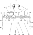
図3、図4において、ゲート端7aとソース端8aを有しパワーMOSFET5aが形成されたパワーMOSFETチップ27と、ベース端9aとエミッタ端10aを有し温度検知トランジスタ3aが形成された温度検知トランジスタチップ28がそれぞれ別体に形成され、この2つのシリコンチップを、たとえば銅材または銅材とセラミック材で複合成形された高熱伝導基材29に半田または高熱伝導性のペースト材で固着し実装してマウントすることによりパワーMOSFETと温度検知トランジスタが同体に形成された複合パワートランジスタを構成する。この状態で温度検知トランジスタ3aのコレクタ端は、パワーMOSFET5aのドレイン端6aと共通となる。
3 and 4, a
このような構成とすることで、パワーMOSFETチップ27の温度は、高熱伝導基材29を伝って数十ミリセカンドから数百ミリセカンドの短い時間に検出可能となる。
With such a configuration, the temperature of the
なお、上記各実施の形態において、パワートランジスタとしてパワーMOSFETチップ27を使って構成したが、シリコンパワー絶縁ゲートバイポーラトランジスタ(IGBT)を使って構成してもよい。
In the above embodiments, the
また、上記各実施形態において、シリコンチップにNPN型を使って構成した例を説明したが、シリコンチップにPNP型を使っても、全ての能動素子および電源の極性を逆にすることによりNPN型の場合と同一の機能を果たすことができる。この場合、温度センサはあくまで温度検知トランジスタ3または3aのベース・エミッタ電圧であるので、集積回路部のラテラルPNPなどのの特性の影響はなく、NPN型と同等の特性を容易に得ることができる。
In each of the embodiments described above, an example in which the NPN type is used for the silicon chip has been described. However, even if the PNP type is used for the silicon chip, the NPN type is obtained by reversing the polarities of all active elements and power sources. The same function as in the case of. In this case, since the temperature sensor is only the base-emitter voltage of the
本発明のパワートランジスタ温度保護装置によれば、パワーMOSFETまたはIGBTと、ある一定の面積のベース領域とエミッタ領域を有する温度検知トランジスタとを、極めて短時間に熱的に結合するとともに、ベース領域とエミッタ領域とをパワーMOSFETまたはIGBTと電気的に絶縁された実装構造を実現したので、パワーMOSFETまたはIGBTの温度を数十ミリセカンドから数百ミリセカンドという短時間に検出できるので、過大な電力印加によってシリコンパワーMOSFETまたはIGBTが熱破壊される臨界温度以下の検出を可能にする優れた温度センサーを提供でき、チップ破壊を未然に防止するものである。 According to the power transistor temperature protection device of the present invention, the power MOSFET or IGBT and the temperature detection transistor having the base region and the emitter region of a certain area are thermally coupled in a very short time, and the base region Since the mounting structure in which the emitter region is electrically insulated from the power MOSFET or IGBT is realized, the temperature of the power MOSFET or IGBT can be detected in a short time of several tens of milliseconds to several hundreds of milliseconds. Thus, it is possible to provide an excellent temperature sensor that enables detection below the critical temperature at which the silicon power MOSFET or IGBT is thermally destroyed, thereby preventing chip destruction.
3,3a 温度検知トランジスタ
4 パワーMOSFETと温度検知トランジスタが同体に形成された複合パワートランジスタシリコンチップ
5、5a パワーMOSFET
6a パワートランジスタのドレイン端
7a パワートランジスタのゲート端
8a パワートランジスタのソース端
9a 温度検知トランジスタのベース端
10a 温度検知トランジスタのエミッタ端
11 電圧オフセット調整用の抵抗
12 別体のシリコンチップで構成されたIC集積回路部
13 ダイオード接続されたトランジスタ
14 電圧源
15、16 抵抗器
17 トランジスタ
18 定電流源
19 温度検知トランジスタのベース・エミッタ電圧検出部
20 温度検出出力トランジスタ
21 プルアップ抵抗
22 温度検知トランジスタのエミッタ端に接続した第1の入力端
23 温度検知トランジスタのベース端に接続した第2の入力端
24 基準グランド端
25 電源端
26 出力端
27 パワーMOSFETチップ
28 温度検知トランジスタチップ
29 高熱伝導基材
30 混成集積回路実装基板
31 ボンディングワイヤー
32 パワーMOSFETのゲート端、
33 パワーMOSFETのソース端
34 パワーMOSFETのドレイン端および温度検知トランジスタのコレクタ端
35 パワーMOSFETのソース電極
36 シリコン酸化膜
37 パワーMOSFETのソース領域を形成するN+高濃度不純物領域
38 温度検知トランジスタのエミッタ領域を形成するN+高濃度不純物領域
39 パワーMOSFETのチャネル領域を形成するP形不純物領域
40 温度検知トランジスタのベース領域を形成するP形不純物領域
41 パワーMOSFETのドレイン高耐圧領域を支配するN−形不純物領域
42 温度検知トランジスタのコレクタ高耐圧領域を形成する−不純物領域
43 パワーMOSFETと温度検知トランジスタを絶縁分離するN+高濃度不純物領域
44 パワーMOSFETと温度検知トランジスタのドレインあるいはコレクタを形成するN+高濃度不純物領域
3, 3a
6a Drain end of power transistor 7a Gate end of power transistor 8a Source end of power transistor 9a Base end of temperature detection transistor 10a Emitter end of
33 Power MOSFET source end 34 Power MOSFET drain end and temperature detection
Claims (4)
前記シリコンパワーMOSFETと同体のシリコンチップ上に形成され前記シリコンパワーMOSFETとは電気的に絶縁されたある一定の面積のベース領域とエミッタ領域とを有する温度検知検知トランジスタと、
前記シリコンパワーMOSFETとは別体の実装基板上に形成され前記温度検知トランジスタのベースとエミッタとの間のベース・エミッタ間電圧が所定の電圧になったことを検出するベース・エミッタ電圧検出部とを備え、
前記ベース・エミッタ電圧検出部は前記温度検知検知トランジスタのベース・エミッタ間電圧の電圧オフセットを調整できるバイアス抵抗を有し前記温度検知トランジスタのベース・エミッタ間電圧から前記シリコンパワーMOSFETが前記バイアス抵抗で任意に設定する所定の温度になったことを検出することを特徴とするパワートランジスタ温度保護装置。 A silicon power MOSFET in which the back surface of the silicon chip is formed as a drain;
A temperature detection and detection transistor having a base area and an emitter area of a certain area formed on a silicon chip that is the same body as the silicon power MOSFET and electrically insulated from the silicon power MOSFET;
A base-emitter voltage detector that is formed on a mounting substrate separate from the silicon power MOSFET and detects that the base-emitter voltage between the base and emitter of the temperature detection transistor has reached a predetermined voltage; With
The base-emitter voltage detection unit has a bias resistor capable of adjusting a voltage offset of the base-emitter voltage of the temperature detection detection transistor, and the silicon power MOSFET is the bias resistance from the base-emitter voltage of the temperature detection transistor. A power transistor temperature protection device for detecting that a predetermined temperature set arbitrarily is detected.
前記シリコンパワートランジスタとは別体のシリコンチップ上に形成され前記シリコンパワートランジスタのドレインと電気的に同電位で熱的に密結合されたコレクタ領域と電気的に絶縁されたある一定の面積のベース領域とエミッタ領域を有する温度検知トランジスタと、
前記シリコンパワートランジスタと前記温度検知トランジスタとは別体の実装基板上に形成され前記温度検知トランジスタのベースとエミッタとの間のベース・エミッタ間電圧が所定の電圧になったことを検出するベース・エミッタ電圧検出部とを備え、
前記ベース・エミッタ電圧検出部は前記温度検知検知トランジスタのベース・エミッタ間電圧の電圧オフセットを調整できるバイアス抵抗を有し前記温度検知トランジスタのベース・エミッタ間電圧から前記シリコンパワートランジスタが前記バイアス抵抗で任意に設定する所定の温度になったことを検出することを特徴とするパワートランジスタ温度保護装置。 A silicon power transistor in which the back surface of the silicon chip is formed as a drain;
A base having a certain area that is formed on a silicon chip separate from the silicon power transistor and is electrically insulated from a collector region that is electrically tightly coupled to the drain of the silicon power transistor at the same potential. A temperature sensing transistor having a region and an emitter region;
The silicon power transistor and the temperature detection transistor are formed on a separate mounting substrate, and a base for detecting that the base-emitter voltage between the base and the emitter of the temperature detection transistor has become a predetermined voltage. An emitter voltage detector,
The base-emitter voltage detection unit has a bias resistor capable of adjusting a voltage offset of the base-emitter voltage of the temperature detection detection transistor, and the silicon power transistor is the bias resistance from the base-emitter voltage of the temperature detection transistor. A power transistor temperature protection device for detecting that a predetermined temperature set arbitrarily is detected.
Priority Applications (1)
| Application Number | Priority Date | Filing Date | Title |
|---|---|---|---|
| JP2004287024A JP2006100690A (en) | 2004-09-30 | 2004-09-30 | Power transistor temperature protective device |
Applications Claiming Priority (1)
| Application Number | Priority Date | Filing Date | Title |
|---|---|---|---|
| JP2004287024A JP2006100690A (en) | 2004-09-30 | 2004-09-30 | Power transistor temperature protective device |
Publications (1)
| Publication Number | Publication Date |
|---|---|
| JP2006100690A true JP2006100690A (en) | 2006-04-13 |
Family
ID=36240180
Family Applications (1)
| Application Number | Title | Priority Date | Filing Date |
|---|---|---|---|
| JP2004287024A Pending JP2006100690A (en) | 2004-09-30 | 2004-09-30 | Power transistor temperature protective device |
Country Status (1)
| Country | Link |
|---|---|
| JP (1) | JP2006100690A (en) |
Cited By (5)
| Publication number | Priority date | Publication date | Assignee | Title |
|---|---|---|---|---|
| WO2010137167A1 (en) * | 2009-05-29 | 2010-12-02 | トヨタ自動車株式会社 | Semiconductor device |
| WO2012029652A1 (en) * | 2010-09-03 | 2012-03-08 | 三菱電機株式会社 | Semiconductor device |
| CN102903702A (en) * | 2011-07-25 | 2013-01-30 | 三菱电机株式会社 | Silicon carbide semiconductor device |
| CN104407640A (en) * | 2014-09-28 | 2015-03-11 | 四川广义微电子股份有限公司 | Temperature self-adaptive adjustment power tube |
| KR20180042410A (en) | 2015-10-01 | 2018-04-25 | 로무 가부시키가이샤 | Semiconductor device |
-
2004
- 2004-09-30 JP JP2004287024A patent/JP2006100690A/en active Pending
Cited By (12)
| Publication number | Priority date | Publication date | Assignee | Title |
|---|---|---|---|---|
| WO2010137167A1 (en) * | 2009-05-29 | 2010-12-02 | トヨタ自動車株式会社 | Semiconductor device |
| WO2012029652A1 (en) * | 2010-09-03 | 2012-03-08 | 三菱電機株式会社 | Semiconductor device |
| CN103098198A (en) * | 2010-09-03 | 2013-05-08 | 三菱电机株式会社 | Semiconductor device |
| JP5372257B2 (en) * | 2010-09-03 | 2013-12-18 | 三菱電機株式会社 | Semiconductor device |
| US8785931B2 (en) | 2010-09-03 | 2014-07-22 | Mitsubishi Electric Corporation | Semiconductor device |
| CN102903702A (en) * | 2011-07-25 | 2013-01-30 | 三菱电机株式会社 | Silicon carbide semiconductor device |
| CN104407640A (en) * | 2014-09-28 | 2015-03-11 | 四川广义微电子股份有限公司 | Temperature self-adaptive adjustment power tube |
| CN104407640B (en) * | 2014-09-28 | 2015-07-29 | 四川广义微电子股份有限公司 | Temperature self-adaptation Modulating Power pipe |
| KR20180042410A (en) | 2015-10-01 | 2018-04-25 | 로무 가부시키가이샤 | Semiconductor device |
| US10964688B2 (en) | 2015-10-01 | 2021-03-30 | Rohm Co., Ltd. | Semiconductor device |
| US11469224B2 (en) | 2015-10-01 | 2022-10-11 | Rohm Co., Ltd. | Semiconductor device |
| US11699698B2 (en) | 2015-10-01 | 2023-07-11 | Rohm Co., Ltd. | Semiconductor device |
Similar Documents
| Publication | Publication Date | Title |
|---|---|---|
| KR930009475B1 (en) | Semiconductor component with power musfet and control circuti | |
| JP5028748B2 (en) | Temperature measurement device for power semiconductor devices | |
| JPH01157573A (en) | Semiconductor device and its manufacture | |
| JP2004207477A (en) | Semiconductor device having hall element | |
| KR102432745B1 (en) | Semiconductor device | |
| JP2011171478A (en) | Semiconductor apparatus | |
| GB2257297A (en) | Sensing current in mos semiconductor devices | |
| TW201126698A (en) | Semiconductor device | |
| US6369654B1 (en) | Semiconductor device | |
| US6906399B2 (en) | Integrated circuit including semiconductor power device and electrically isolated thermal sensor | |
| KR100272052B1 (en) | Power transistor | |
| JP2006100690A (en) | Power transistor temperature protective device | |
| JP2011108684A (en) | Semiconductor device | |
| JP2005026279A (en) | Semiconductor device | |
| JP2004319861A (en) | Semiconductor device | |
| JP2007287919A (en) | Semiconductor device with temperature detection function | |
| JP2010199149A (en) | Semiconductor device | |
| JPH03188661A (en) | Resin seal type semiconductor device | |
| JPS63299264A (en) | Semiconductor device | |
| JP3042256B2 (en) | Power transistor temperature protection circuit device | |
| JP2854900B2 (en) | Semiconductor device | |
| JPH0834221B2 (en) | Semiconductor device with current detection function | |
| JPH08236709A (en) | Semiconductor device | |
| JPH053289A (en) | Power semiconductor device | |
| JP2004146628A (en) | Semiconductor device |