EP1785708B1 - Composant de capteur de pression - Google Patents
Composant de capteur de pression Download PDFInfo
- Publication number
- EP1785708B1 EP1785708B1 EP06400035.9A EP06400035A EP1785708B1 EP 1785708 B1 EP1785708 B1 EP 1785708B1 EP 06400035 A EP06400035 A EP 06400035A EP 1785708 B1 EP1785708 B1 EP 1785708B1
- Authority
- EP
- European Patent Office
- Prior art keywords
- housing part
- pressure sensor
- chip
- opening
- sensor element
- Prior art date
- Legal status (The legal status is an assumption and is not a legal conclusion. Google has not performed a legal analysis and makes no representation as to the accuracy of the status listed.)
- Active
Links
- 239000004020 conductor Substances 0.000 claims description 33
- 239000012528 membrane Substances 0.000 claims description 25
- 239000004033 plastic Substances 0.000 claims description 3
- 229920003023 plastic Polymers 0.000 claims description 3
- 230000035945 sensitivity Effects 0.000 claims description 2
- 239000011796 hollow space material Substances 0.000 claims 1
- 238000009530 blood pressure measurement Methods 0.000 description 16
- NJPPVKZQTLUDBO-UHFFFAOYSA-N novaluron Chemical compound C1=C(Cl)C(OC(F)(F)C(OC(F)(F)F)F)=CC=C1NC(=O)NC(=O)C1=C(F)C=CC=C1F NJPPVKZQTLUDBO-UHFFFAOYSA-N 0.000 description 7
- 238000004519 manufacturing process Methods 0.000 description 6
- 239000004065 semiconductor Substances 0.000 description 6
- 239000000969 carrier Substances 0.000 description 4
- 238000000034 method Methods 0.000 description 4
- 239000002775 capsule Substances 0.000 description 3
- 238000011156 evaluation Methods 0.000 description 3
- 238000001465 metallisation Methods 0.000 description 3
- 239000002991 molded plastic Substances 0.000 description 3
- 238000004382 potting Methods 0.000 description 3
- 229910052710 silicon Inorganic materials 0.000 description 3
- 239000010703 silicon Substances 0.000 description 3
- 239000000243 solution Substances 0.000 description 3
- 150000001875 compounds Chemical class 0.000 description 2
- 238000005516 engineering process Methods 0.000 description 2
- 239000011521 glass Substances 0.000 description 2
- 238000002347 injection Methods 0.000 description 2
- 239000007924 injection Substances 0.000 description 2
- 238000012545 processing Methods 0.000 description 2
- 230000001681 protective effect Effects 0.000 description 2
- ONBQEOIKXPHGMB-VBSBHUPXSA-N 1-[2-[(2s,3r,4s,5r)-3,4-dihydroxy-5-(hydroxymethyl)oxolan-2-yl]oxy-4,6-dihydroxyphenyl]-3-(4-hydroxyphenyl)propan-1-one Chemical compound O[C@@H]1[C@H](O)[C@@H](CO)O[C@H]1OC1=CC(O)=CC(O)=C1C(=O)CCC1=CC=C(O)C=C1 ONBQEOIKXPHGMB-VBSBHUPXSA-N 0.000 description 1
- 238000010923 batch production Methods 0.000 description 1
- 229940126142 compound 16 Drugs 0.000 description 1
- 238000013461 design Methods 0.000 description 1
- 230000000694 effects Effects 0.000 description 1
- 239000013013 elastic material Substances 0.000 description 1
- 229910000679 solder Inorganic materials 0.000 description 1
Images

Classifications
-
- G—PHYSICS
- G01—MEASURING; TESTING
- G01L—MEASURING FORCE, STRESS, TORQUE, WORK, MECHANICAL POWER, MECHANICAL EFFICIENCY, OR FLUID PRESSURE
- G01L9/00—Measuring steady of quasi-steady pressure of fluid or fluent solid material by electric or magnetic pressure-sensitive elements; Transmitting or indicating the displacement of mechanical pressure-sensitive elements, used to measure the steady or quasi-steady pressure of a fluid or fluent solid material, by electric or magnetic means
- G01L9/0041—Transmitting or indicating the displacement of flexible diaphragms
- G01L9/0051—Transmitting or indicating the displacement of flexible diaphragms using variations in ohmic resistance
- G01L9/0052—Transmitting or indicating the displacement of flexible diaphragms using variations in ohmic resistance of piezoresistive elements
- G01L9/0055—Transmitting or indicating the displacement of flexible diaphragms using variations in ohmic resistance of piezoresistive elements bonded on a diaphragm
-
- G—PHYSICS
- G01—MEASURING; TESTING
- G01L—MEASURING FORCE, STRESS, TORQUE, WORK, MECHANICAL POWER, MECHANICAL EFFICIENCY, OR FLUID PRESSURE
- G01L19/00—Details of, or accessories for, apparatus for measuring steady or quasi-steady pressure of a fluent medium insofar as such details or accessories are not special to particular types of pressure gauges
- G01L19/0007—Fluidic connecting means
- G01L19/0038—Fluidic connecting means being part of the housing
-
- G—PHYSICS
- G01—MEASURING; TESTING
- G01L—MEASURING FORCE, STRESS, TORQUE, WORK, MECHANICAL POWER, MECHANICAL EFFICIENCY, OR FLUID PRESSURE
- G01L19/00—Details of, or accessories for, apparatus for measuring steady or quasi-steady pressure of a fluent medium insofar as such details or accessories are not special to particular types of pressure gauges
- G01L19/0061—Electrical connection means
- G01L19/0084—Electrical connection means to the outside of the housing
-
- G—PHYSICS
- G01—MEASURING; TESTING
- G01L—MEASURING FORCE, STRESS, TORQUE, WORK, MECHANICAL POWER, MECHANICAL EFFICIENCY, OR FLUID PRESSURE
- G01L19/00—Details of, or accessories for, apparatus for measuring steady or quasi-steady pressure of a fluent medium insofar as such details or accessories are not special to particular types of pressure gauges
- G01L19/14—Housings
- G01L19/141—Monolithic housings, e.g. molded or one-piece housings
-
- G—PHYSICS
- G01—MEASURING; TESTING
- G01L—MEASURING FORCE, STRESS, TORQUE, WORK, MECHANICAL POWER, MECHANICAL EFFICIENCY, OR FLUID PRESSURE
- G01L19/00—Details of, or accessories for, apparatus for measuring steady or quasi-steady pressure of a fluent medium insofar as such details or accessories are not special to particular types of pressure gauges
- G01L19/14—Housings
- G01L19/148—Details about the circuit board integration, e.g. integrated with the diaphragm surface or encapsulation
-
- H—ELECTRICITY
- H01—ELECTRIC ELEMENTS
- H01L—SEMICONDUCTOR DEVICES NOT COVERED BY CLASS H10
- H01L2224/00—Indexing scheme for arrangements for connecting or disconnecting semiconductor or solid-state bodies and methods related thereto as covered by H01L24/00
- H01L2224/01—Means for bonding being attached to, or being formed on, the surface to be connected, e.g. chip-to-package, die-attach, "first-level" interconnects; Manufacturing methods related thereto
- H01L2224/42—Wire connectors; Manufacturing methods related thereto
- H01L2224/47—Structure, shape, material or disposition of the wire connectors after the connecting process
- H01L2224/48—Structure, shape, material or disposition of the wire connectors after the connecting process of an individual wire connector
- H01L2224/4805—Shape
- H01L2224/4809—Loop shape
- H01L2224/48091—Arched
-
- H—ELECTRICITY
- H01—ELECTRIC ELEMENTS
- H01L—SEMICONDUCTOR DEVICES NOT COVERED BY CLASS H10
- H01L2224/00—Indexing scheme for arrangements for connecting or disconnecting semiconductor or solid-state bodies and methods related thereto as covered by H01L24/00
- H01L2224/01—Means for bonding being attached to, or being formed on, the surface to be connected, e.g. chip-to-package, die-attach, "first-level" interconnects; Manufacturing methods related thereto
- H01L2224/42—Wire connectors; Manufacturing methods related thereto
- H01L2224/47—Structure, shape, material or disposition of the wire connectors after the connecting process
- H01L2224/49—Structure, shape, material or disposition of the wire connectors after the connecting process of a plurality of wire connectors
- H01L2224/491—Disposition
- H01L2224/4912—Layout
- H01L2224/49171—Fan-out arrangements
Definitions
- the invention relates to pressure sensor components.
- the medium to be measured acts directly on the protective membrane.
- the electrical contact is made with embedded and out leading electrical conductors. For mounting on a carrier, these capsules are not provided.
- the solutions in the pamphlets DE 196 26 084 C2 (Pressure sensor device for mounting on the mounting surface of a printed circuit board) and DE 197 24 026 A1 (Pressure sensor device and method of manufacture) are suitable for mounting and contacting on a circuit board as a carrier.
- the contacting takes place via the chip carrier, wherein the end region of the leadframe used are guided to the outside and end there freely accessible.
- the sensor for measuring pressure is located inside the respective device, wherein the medium to be measured acts on a region of the device.
- the medium acts on a gel between the cover and pressure sensor or on the cover of the pressure sensor itself.
- the gel or the Cover a pressure transmitter between medium and pressure sensor.
- These solutions are only suitable for absolute pressure measurement.
- the publication JP2003130749 discloses a pressure sensor device having a trough-shaped housing part and an opening for a pressure sensor element in a carrier surface.
- the indicated in claim 1 invention has for its object to provide a simple to implement, economically inexpensive to manufacture, compact and easy-to-handle component as a pressure sensor.
- the pressure sensor components are characterized in particular by a simple and compact realization with universal application possibility.
- the first housing part has at least one support surface on which the at least one pressure sensor element is located.
- the support surface is at the same time a component of the first housing part.
- the carrier surface forming part of the first housing part has at least one opening for the pressure sensor element, wherein the opening is located in the bottom area of the first housing part.
- the medium to be measured abuts the pressure sensor element via the opening.
- the use of an MID housing results in a compact pressure sensor device that has few components.
- the first housing part leads to easy handling and connectivity of the pressure sensor element.
- a second plate-shaped housing part or a body is arranged, wherein the wall of the first housing part projects beyond the second housing part or the body and either on the edge surface of the wall of the first Housing part or a wall area comprehensive and thus on an outer wall portion of the first housing part terminating conductor tracks are simultaneously terminal contacts.
- the end regions are advantageously simultaneously the electrical contacts of the pressure sensor component to the outside.
- the body in the first housing part is, for example, a potting compound for protecting the pressure sensor element including its contacting in the first housing part.
- the housing part as an MID housing is further distinguished by the fact that it can be produced as a plastic injection molded part easily and economically even in large quantities as a mass product. This injection molded body is provided with a structured metallization with conductor tracks, so that the housing part itself is a circuit carrier.
- the injection-molded body is coated with a known metal deposition, with different properties of the plastics used to effect a selective metallization and the structured pattern is formed.
- the pressure sensor device can be easily manufactured and provided as a mass product. Due to the simple structure, such a structure is suitable both for a manual small batch production as well as for a machine mass production. In the latter case, a production line with assembly stations and assembly stations can be used.
- the one part of the first housing part performing carrier surface has a first opening for the pressure sensor element and the first housing part at least a second opening adjacent to the support surface, wherein the openings are in the bottom portion of the first housing part.
- the second plate-shaped housing part is arranged in the first housing part, wherein the wall of the first housing part projects beyond the second housing part, between the pressure sensor element and the second housing part at least one opening via the second opening cavity is present and either on the edge surface of the wall of the first housing part or a wall portion comprehensive and thus on an outer wall region of the first housing part-terminating conductor tracks are simultaneously terminal contacts.
- the first housing part is provided with a second plate-shaped housing part such that the second housing part is arranged at a distance from the pressure sensor element.
- the pressure sensor component can advantageously be easily used either for absolute pressure measurement or for differential pressure measurement.
- the first housing part is completed, wherein the medium to be measured rests on the pressure sensor element via the opening.
- the first housing part is provided with the second housing part such that two media engage the pressure sensor element.
- the first medium can attack via the opening on one side of the pressure sensor element, while the second medium passes through at least one opening, for example as a recess or opening of the second housing part and the cavity present through the gap between the first housing part and pressure sensor element to the other side of the pressure sensor element ,
- a housing design can be easily used for very different applications, so that a universal use is given.
- the interconnects end according to the embodiment of claim 3 on comb-like elevations of the wall of the housing part, so that a slight mechanical electrical contacting in the form of solder joints of the pressure sensor component is possible.
- the elevations advantageously lead to adjacent interconnects are not connected to each other in this contact.
- SMT SMT
- a connection fitting for the opening or a plurality of connection fittings for the openings according to the embodiment of claim 4 ensures or ensure easy handling of the pressure sensor device with respect to the connection of the medium.
- a hose can be easily pushed, with at least one mounting clamp for the hose can be applied.
- a connection fitting ensures a firm and secure hold of the hose line.
- the second housing part is according to the embodiment of claim 5, a component carrier with conductor tracks and thus even a circuit carrier.
- a component carrier with conductor tracks and thus even a circuit carrier.
- special and user-specific circuit variants for evaluating the measured values can be realized.
- the housing parts can easily be designed so that at the same time correspondingly arranged conductor tracks are interconnected electrically conductive in the connection of these parts.
- At least one component carrier with conductor tracks and at least one chip with an integrated circuit and / or at least one electronic component and thus a circuit carrier is arranged according to the embodiment of claim 6 between the bottom of the first housing part and the second housing part and with conductor tracks of wall portions of the first housing part connected.
- the component carriers can be designed user-specific, wherein a wide variety of circuit variants can be realized.
- the first housing part is further arranged according to the embodiment of claim 7 at least one chip with an integrated circuit and connected to tracks of this housing part.
- the integrated circuit is advantageously a data processing system, so that the measured data is processed in the pressure sensor component can be.
- an intelligent pressure sensor component is realized.
- Such a device can thus also be manufactured application-specific.
- These are further arranged side by side either in a plane or in different planes in the first housing part. This leads to a simple and economical production of the pressure sensor component.
- the surfaces of the chip as a pressure sensor element and the chip with an integrated circuit can advantageously be in one plane.
- the connection of the respective chip with conductor tracks preferably takes place by means of bonded wire bridges.
- This provides an intelligent pressure sensor component.
- special pressure sensor elements as well as electronic components and / or circuit carriers, for example, as a chip with an integrated circuit in the form of an evaluation circuit, a wide variety of applications can be easily realized.
- the pressure sensor element is located between the pressure sensor element and the second housing part, a cavity, a body, a medium or a reference vacuum.
- the cavity, body, medium or vacuum are a reference of the pressure sensor device.
- the body is located in the cavity between the pressure sensor element and the second housing part.
- At least one corner region of walls of the first housing part of the pressure sensor component has according to the embodiment of claim 9 an increase.
- This increase is located on adjacent walls and advantageously represents an assembly aid and / or a mechanical fastening possibility for the pressure sensor component.
- This increase is advantageously a pin, a hook or a part with a clamping mechanism.
- the pressure sensor element is according to the embodiment of claim 10, a chip with a thinned region as a membrane on a pedestal.
- the membrane has at least one electrical strain that changes its electrical resistance when stretched Element on.
- the base has a through opening. This opening and the opening in the first housing part cause the medium can reach the membrane of the pressure sensor element.
- the use of a socket facilitates the handling of the pressure sensor element.
- different cross-sections of the membrane and the openings can be easily realized.
- the cross-section and the thickness of the membrane determine the sensitivity of the pressure sensor element.
- the element is advantageously a semiconductor measuring element as an integral part of the pressure sensor element. With these features, the pressure sensor component is advantageously suitable for absolute and / or differential and / or gauge pressure measurement.
- At least the region of the membrane on the side adjacent to the medium to be measured and covered with a hood-like body and the limited by the membrane and the body cavity has a reference volume.
- a hood-like body simultaneously protects at least the pressure-sensitive area of the pressure sensor element against an adjacent medium in the pressure sensor component.
- the membrane of the pressure sensor element in particular is separated from the medium in the pressure sensor component.
- the pressure sensor component for measuring the absolute pressure can be used particularly advantageously for pressure measurement under difficult media conditions.
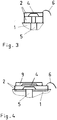
- a pressure sensor component of a first embodiment essentially consists of a first trough-shaped housing part 1 with conductor tracks 3 and a pressure sensor element 2.
- the Fig. 1 shows the pressure sensor device in a plan view.
- This support surface is part of the bottom region of the housing part 1 and has an opening 5 for the pressure sensor element 2, so that the medium reaches the pressure sensor element 2 via the opening 5 in the bottom region of the housing part 1 can (representation in the Fig. 3 ).
- the opening 5 is provided with a connection fitting 8, which is at the same time a component of the first housing part 1 (illustration in FIG Fig. 2 ).
- the pressure sensor element 2 is a chip of silicon with a thinned region as the membrane 4.
- the membrane 4 is provided with at least one element as a semiconductor element in the form of a semiconductor resistor, wherein upon expansion, a proportional electrical resistance change occurs.
- the element is part of a known measuring bridge, wherein an electrical resistance change, for example, causes a proportional electrical voltage change.
- the element with contacts of the chip as a pressure sensor element 2 is electrically connected.
- the chip as a pressure sensor element 2 is located on a pedestal and / or a pedestal whose cross section is equal to, smaller or larger than that of the chip as a pressure sensor element 2.
- the base and / or the pedestal has a through opening, said opening and the opening 5 of the housing part 1 enclose a cavity.
- the cross sections of the thinned region as membrane 4 is larger (shown in FIG Fig.
- the contacts of the chip as a pressure sensor element 2 are connected via bonded wire bridges 6 with leading conductors 3 as connection contacts 7 of the pressure sensor component.
- a body preferably as a hardened potting compound, or a second plate-shaped housing part 14 in the first housing part 1, wherein the wall of the first housing part 1 projects beyond the body or the second housing part 14.
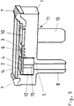
- a pressure sensor component essentially consists of a first trough-shaped housing part 1 as circuit carrier with a pressure sensor element 2 and a chip 10 and / or at least one electronic component and a second plate-shaped housing part 14 in a second exemplary embodiment.
- the Fig. 5 shows the pressure sensor component in a sectional view.
- This support surface is part of the bottom region of the first housing part 1 and has a first opening 5 for the pressure sensor element 2, so that the medium via the first opening 5 in the bottom region of the first housing part 1 can get to the pressure sensor element 2.
- the first housing part 1 has in the bottom area a second opening 11 adjacent to the support surfaces for the pressure sensor element 2 and the chip 10 with an evaluation.
- the first opening 5 and the second opening 11 are provided with connection fittings 8, 13, which are at the same time a component of the first housing part 1.
- the pressure sensor element 2 is a chip of silicon with a thinned region as the membrane 4.
- the membrane 4 is provided with at least one element as a semiconductor element in the form of a semiconductor resistor, wherein upon expansion, a proportional electrical resistance change occurs.
- the element is part of a known measuring bridge, wherein an electrical resistance change, for example, causes a proportional electrical voltage change.
- the element with contacts of the chip as a pressure sensor element 2 is electrically connected.
- the chip as a pressure sensor element 2 is located on a base 3 whose cross section is equal to or smaller than that of the chip as a pressure sensor element 2.
- the base 12 may either be a body or consist of several interconnected bodies.
- the support surface may be the surface of a pedestal for the pressure sensor element 2, which is at the same time a component of the first housing part 1.
- the base 12 and / or the pedestal has a through opening 15, said opening 15 and the first opening 5 of the first housing part 1 enclose a cavity.
- the cross sections of the thinned region as membrane 4 is larger (shown in FIG Fig. 3 ), equal to or smaller than that of the openings 5, 15.
- the chip as a pressure sensor element 2 and the chip 10 with an integrated circuit are arranged side by side in the first housing part 1 so that the surfaces of the chip as a pressure sensor element 2 and the chip 10 with an integrated circuit are in a plane (shown in FIG Fig. 5 ).
- other electronic components can be placed in the first housing part 1.
- the contacts of the chip as pressure sensor element 2 and the chip 10 with an integrated circuit are connected depending on the circuit via bonded wire bridges 6 and interconnects 3 with each other and via bonded wire bridges 6 and outwardly leading interconnects 3 as terminal contacts 7 of the pressure sensor component.
- printed conductors 3 end on the edge surface of the wall of the first housing part 1.
- these printed conductors 3 end on comb-like elevations of the wall of the first housing part 1 or are guided over them so that they end on an outer wall area. In one embodiment, these may also be themselves as such elevations be educated. This ensures that these interconnects 3 can be contacted as connecting contacts when placing the pressure sensor component on a printed circuit board with conductor tracks.
- the first housing part 1 is closed with a second plate-shaped housing part 14 such that the second housing part 14 is arranged at a distance from the pressure sensor element 2 and thus at least one cavity which is open via the second opening 11 is present.
- At least the region of the membrane 4 on the side opposite the adjacent medium to be measured can be covered with a hood-like body 9, preferably as a glass body.
- a hood-like body 9 preferably as a glass body.
- the limited by the membrane 4 and this body 9 cavity has a reference volume, in particular with a reference vacuum (representation in the Fig. 4 ). This realizes a pressure sensor component for absolute pressure measurement.
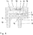
- a pressure sensor component for absolute and / or differential and / or gauge pressure measurement consists in a third embodiment substantially of a first trough-shaped housing part 1 with a pressure sensor element 2 and a second plate-shaped housing part 14 as a circuit carrier with at least one chip 10, for example as an electronic Evaluation circuit and / or at least one electronic component.
- the Fig. 6 shows the pressure sensor component in a sectional view.
- the pressure sensor element 2 connected to printed conductors 3 via bonded wire bridges 6 is located on the carrier surface.
- This carrier surface is at the same time a component of the bottom region of the first Housing part 1 and has a first opening 5 for the pressure sensor element 2, so that the medium can pass through this first opening 5 to the pressure sensor element 2.
- the first housing part 1 has in the bottom region a second opening 11 adjacent to the support surface for the pressure sensor element 2.
- the first opening 5 and the second opening 11 are provided with connection fittings 8, 13, which are at the same time a part of the first housing part 1.
- the pressure sensor element 2 is a chip of silicon with a thinned region as a membrane 4 having at least one element as a semiconductor element on a base 3 corresponding to that of the first embodiment.
- conductor tracks of the first housing part 1 are led to the outside. The end regions are simultaneously formed as connection contacts 7 of this pressure sensor component.
- the first housing part 1 is closed with a second plate-shaped housing part 14 such that the second housing part 14 is arranged at a distance from the pressure sensor element 2 and at least one cavity which is open via the second opening 11 is present. This realizes a pressure sensor component for absolute and / or differential and / or gauge pressure measurement.
- conductor tracks are led to the end regions of the first housing part 1.
- the first housing part 1 is closed with a second plate-shaped housing part 14 such that between the pressure sensor element 2 and the second housing part 14 there is at least one cavity open via the second opening 11.
- the second housing part 14 is formed as a circuit carrier.
- at least one chip 10 with an integrated circuit and / or at least one electronic component and conductor tracks are arranged on the second housing part 14.
- Conductor tracks of the second housing part 14 are connected via edge regions with conductor tracks of the first housing part 1. Further interconnects terminate on the second housing part 14. End regions are simultaneously formed as contacts 7 for the pressure sensor component.
- the chip 10 with an integrated circuit, the printed conductors on the second housing part 14 and the bonded wire bridges 6 for electrically connecting the printed conductors to the integrated circuit of the chip 10 and / or the at least one electronic component are embedded in a potting compound 16.
- a pressure sensor component shows the Fig. 6 ,
- At least the region of the membrane 4 on the side opposite the adjacent and to be measured medium can be covered with a hood-like body 9, in particular as a glass body.
- a hood-like body 9 in particular as a glass body.
- the limited by the membrane 4 and this body 9 cavity has a reference volume advantageously enough with a reference vacuum (shown in the Fig. 4 ). This realizes a pressure sensor component for absolute pressure measurement.
- TAB tape automated bonding
- a body, a medium or a reference vacuum can be located between the pressure sensor element 2 and the second housing part 14.
- the medium may advantageously be a gel and the body made of an elastic material.
- At least one corner region of walls of the first housing part 1 of the pressure sensor component can have an increase.
- This increase is located on adjacent walls and advantageously constitutes an assembly aid and / or a mechanical fastening possibility for the pressure sensor component.
- this elevation is a pin, a hook or a part with a clamping mechanism.
- This increase can thus be easily inserted and fixed in an opening of a support for the pressure sensor component.
- the increase for example, a conical pin with at least one circumferential recess and / or increase, so that in conjunction with the opening and the support of the pressure sensor component, a snap mechanism is realized.
Claims (6)
- Élément structurel à capteur de pression destiné à la mesure de la pression différentielle comprenant les propriétés suivantes :- une première partie de boîtier (1) en forme de cuve qui se présente sous la forme d'une partie en plastique moulée par injection, comprenant aussi bien des pistes conductrices (3), qui se présentent sous la forme d'une partie de boîtier MID (MID = molded interconnect device), que tout au moins une surface de support à l'intérieur ;- un élément à capteur de pression (2) qui est relié aux pistes conductrices (3) et qui se présente sous la forme d'une puce avec une zone amincie qui se présente sous la forme d'une membrane (4) située sur un socle (12) se trouvant sur la surface de support, la membrane (4) présentant tout au moins un élément qui modifie sa résistance électrique en cas de dilatation et l'élément étant relié de manière électriquement conductrice à des contacts de la puce, sous la forme d'un élément à capteur de pression (2), et la section transversale et l'épaisseur de la membrane déterminant la sensibilité de l'élément structurel à capteur de pression ;- une première ouverture (5) pour l'élément à capteur de pression (2) se trouvant dans la surface de support, sous la forme d'un élément constitutif de la première partie de boîtier (1) qui se trouve en liaison avec une ouverture (15) traversante dans le socle (12), les sections transversales de la membrane (4) et des ouvertures (5, 15) étant identiques ou différentes ;- au moins une deuxième ouverture (11) située dans la première partie de boîtier (1), à côté de la surface de support, les ouvertures (5, 11) se trouvant au niveau du fond de la première partie de boîtier (1) ;- une deuxième partie de boîtier (14), en forme de plaque, située dans la première partie de boîtier (1), la paroi de la première partie de boîtier (1) dépassant la deuxième partie de boîtier (14), tout au moins une cavité ouverte par l'intermédiaire de la deuxième ouverture (11) étant présente entre l'élément à capteur de pression (2) et la deuxième partie de boîtier (14) ; et- des pistes conductrices (3), qui se présentent sous la forme de contacts de connexion (7) simultanés, de fixations ou sous la forme de contacts de connexion (7) et de fixations et qui se terminent sur des élévations de la paroi de la première partie de boîtier (1), lesquelles élévations ont la forme d'un peigne.
- Élément structurel à capteur de pression selon la revendication de brevet 1, caractérisé en ce que la première partie de boîtier (1) possède des raccords de branchement (8, 13) pour la première ouverture (5) et pour la deuxième ouverture (11).
- Élément structurel à capteur de pression selon la revendication de brevet 1, caractérisé en ce que la deuxième partie de boîtier (14) est un support pour élément structurel qui comprend des pistes conductrices et tout au moins une puce (10) dotée d'un circuit intégré et/ou qui comprend au moins un élément structurel électronique et, par conséquent, un support de circuit.
- Élément structurel à capteur de pression selon la revendication de brevet 1, caractérisé en ce que tout au moins un élément de support pour élément structurel qui comprend des pistes conductrices et tout au moins une puce (10) comportant un circuit intégré et/ou qui comprend au moins un élément structurel électronique et, par conséquent, un support de circuit est disposé entre le fond de la première partie de boîtier (1) et la deuxième partie de boîtier (14) et est relié à des pistes conductrices des surfaces de paroi de la première partie de boîtier (1).
- Élément structurel à capteur de pression selon la revendication de brevet 1, caractérisé en ce que tout au moins une puce (10) qui comprend un circuit intégré est disposée dans la première partie de boîtier (1) et est reliée à des pistes conductrices (3), la puce qui se présente sous la forme d'un élément à capteur de pression (2) et la puce (10) comportant un circuit intégré étant disposées l'une à côté de l'autre dans la première partie de boîtier (1), soit au même niveau, soit à des niveaux différents.
- Élément structurel à capteur de pression selon la revendication de brevet 1, caractérisé en ce que tout au moins une zone de coin des parois de la première partie de boîtier (1) présente une élévation, l'élévation étant un tenon, un crochet ou une pièce comprenant un mécanisme de serrage.
Applications Claiming Priority (4)
| Application Number | Priority Date | Filing Date | Title |
|---|---|---|---|
| DE202005017627U DE202005017627U1 (de) | 2005-11-09 | 2005-11-09 | Drucksensor-Bauelement |
| DE102005053876A DE102005053876B4 (de) | 2005-11-09 | 2005-11-09 | Drucksensor-Bauteil |
| DE200510053877 DE102005053877B4 (de) | 2005-11-09 | 2005-11-09 | Drucksensor-Bauelement |
| DE202005017626U DE202005017626U1 (de) | 2005-11-09 | 2005-11-09 | Drucksensor-Bauteil |
Publications (3)
| Publication Number | Publication Date |
|---|---|
| EP1785708A2 EP1785708A2 (fr) | 2007-05-16 |
| EP1785708A3 EP1785708A3 (fr) | 2009-12-30 |
| EP1785708B1 true EP1785708B1 (fr) | 2018-01-03 |
Family
ID=37734824
Family Applications (1)
| Application Number | Title | Priority Date | Filing Date |
|---|---|---|---|
| EP06400035.9A Active EP1785708B1 (fr) | 2005-11-09 | 2006-11-07 | Composant de capteur de pression |
Country Status (1)
| Country | Link |
|---|---|
| EP (1) | EP1785708B1 (fr) |
Families Citing this family (5)
| Publication number | Priority date | Publication date | Assignee | Title |
|---|---|---|---|---|
| DE102010003724A1 (de) * | 2010-04-08 | 2011-10-13 | Robert Bosch Gmbh | Drucksensoranordnung |
| US9021689B2 (en) | 2011-06-02 | 2015-05-05 | Freescale Semiconductor, Inc. | Method of making a dual port pressure sensor |
| US8307714B1 (en) * | 2011-06-02 | 2012-11-13 | Freescale Semiconductor, Inc. | Dual port pressure sensor |
| EP2916120A1 (fr) * | 2014-03-04 | 2015-09-09 | seleon GmbH | Bloc de capteur, tube et procédé de fabrication |
| RU2609223C1 (ru) * | 2015-10-08 | 2017-01-31 | Акционерное общество "Научно-исследовательский институт Авиационного оборудования" | Тензорезисторный датчик абсолютного давления на основе кни микроэлектромеханической системы |
Family Cites Families (7)
| Publication number | Priority date | Publication date | Assignee | Title |
|---|---|---|---|---|
| JP3209118B2 (ja) * | 1996-05-30 | 2001-09-17 | 松下電工株式会社 | 圧力センサパッケージ本体及びその製造方法 |
| DE19626084C2 (de) * | 1996-06-28 | 2003-04-17 | Infineon Technologies Ag | Drucksensorvorrichtung für eine Montage auf der Bestückungsoberfläche einer Leiterplatte |
| JP3209119B2 (ja) * | 1996-07-30 | 2001-09-17 | 松下電工株式会社 | 圧力センサ |
| JP2003133453A (ja) * | 2001-10-29 | 2003-05-09 | Matsushita Electric Works Ltd | 圧力センサ |
| JP2003130742A (ja) * | 2001-10-29 | 2003-05-08 | Matsushita Electric Works Ltd | 半導体圧力センサ |
| JP3627693B2 (ja) * | 2001-10-29 | 2005-03-09 | 松下電工株式会社 | 圧力センサ |
| JP2003130749A (ja) * | 2001-10-29 | 2003-05-08 | Matsushita Electric Works Ltd | 圧力センサ |
-
2006
- 2006-11-07 EP EP06400035.9A patent/EP1785708B1/fr active Active
Non-Patent Citations (1)
| Title |
|---|
| None * |
Also Published As
| Publication number | Publication date |
|---|---|
| EP1785708A2 (fr) | 2007-05-16 |
| EP1785708A3 (fr) | 2009-12-30 |
Similar Documents
| Publication | Publication Date | Title |
|---|---|---|
| DE102014200093A1 (de) | Sensor zur Erfassung einer Temperatur und eines Drucks eines fluiden Mediums | |
| EP1728060B1 (fr) | Module de capteurs comportant une protection de compatibilite electromagnetique et contre les decharges electrostatiques a condensateurs | |
| EP1797437B1 (fr) | Appareil servant a determiner des grandeurs electriques | |
| DE10352917A1 (de) | Sensoranordnung mit mehreren potentiometrischen Sensoren | |
| EP0935743B1 (fr) | Unite capteur de pression, en particulier pour la technologie automobile | |
| WO1989008243A1 (fr) | Dispositif de mesure de pression | |
| EP1785708B1 (fr) | Composant de capteur de pression | |
| DE10014992A1 (de) | Sensoranordnung | |
| DE102014219030B4 (de) | Steckermodul | |
| DE102005053876B4 (de) | Drucksensor-Bauteil | |
| DE102014118769B4 (de) | Drucksensor-Modul mit einem Sensor-Chip und passiven Bauelementen innerhalb eines gemeinsamen Gehäuses | |
| DE102007000813B4 (de) | Mit einem Verbinder integrierter Sensor und Verfahren zum Herstellen von diesem | |
| DE102007054717B4 (de) | Transmitter und Verfahren zur Herstellung eines Transmitters | |
| DE202005017626U1 (de) | Drucksensor-Bauteil | |
| DE102005020345A1 (de) | Dichtungsstruktur für einen Verbinder | |
| DE102007041785A1 (de) | Halbleitervorrichtung und deren Herstellungsverfahren | |
| DE102013220091A1 (de) | Drucksensor | |
| DE3200448C2 (de) | Verfahren zur Herstellung einer Halbleiter-Druckwandleranordnung | |
| DE102005053877B4 (de) | Drucksensor-Bauelement | |
| WO2020187370A1 (fr) | Ensemble de capteur comprenant un élément de capteur de température, et procédé pour sa fabrication | |
| EP1353160B1 (fr) | Capteur de pression | |
| DE102013223542A1 (de) | Elektronische Einheit mit Leiterplatte | |
| DE19902450B4 (de) | Miniaturisiertes elektronisches System und zu dessen Herstellung geeignetes Verfahren | |
| DE202005017627U1 (de) | Drucksensor-Bauelement | |
| DE102017218893A1 (de) | Sensoranordnung zur Bestimmung wenigstens eines Parameters eines durch einen Messkanal strömenden fluiden Mediums |
Legal Events
| Date | Code | Title | Description |
|---|---|---|---|
| PUAI | Public reference made under article 153(3) epc to a published international application that has entered the european phase |
Free format text: ORIGINAL CODE: 0009012 |
|
| AK | Designated contracting states |
Kind code of ref document: A2 Designated state(s): AT BE BG CH CY CZ DE DK EE ES FI FR GB GR HU IE IS IT LI LT LU LV MC NL PL PT RO SE SI SK TR |
|
| AX | Request for extension of the european patent |
Extension state: AL BA HR MK YU |
|
| PUAL | Search report despatched |
Free format text: ORIGINAL CODE: 0009013 |
|
| AK | Designated contracting states |
Kind code of ref document: A3 Designated state(s): AT BE BG CH CY CZ DE DK EE ES FI FR GB GR HU IE IS IT LI LT LU LV MC NL PL PT RO SE SI SK TR |
|
| AX | Request for extension of the european patent |
Extension state: AL BA HR MK RS |
|
| 17P | Request for examination filed |
Effective date: 20100623 |
|
| 17Q | First examination report despatched |
Effective date: 20100721 |
|
| AKX | Designation fees paid |
Designated state(s): AT BE BG CH CY CZ DE DK EE ES FI FR GB GR HU IE IS IT LI LT LU LV MC NL PL PT RO SE SI SK TR |
|
| AXX | Extension fees paid |
Extension state: AL Payment date: 20100623 Extension state: BA Payment date: 20100623 Extension state: RS Payment date: 20100623 |
|
| RAP1 | Party data changed (applicant data changed or rights of an application transferred) |
Owner name: HARTING AG Owner name: AKTIV SENSOR GMBH |
|
| REG | Reference to a national code |
Ref country code: DE Ref legal event code: R079 Ref document number: 502006015770 Country of ref document: DE Free format text: PREVIOUS MAIN CLASS: G01L0009000000 Ipc: G01L0019000000 |
|
| GRAP | Despatch of communication of intention to grant a patent |
Free format text: ORIGINAL CODE: EPIDOSNIGR1 |
|
| STAA | Information on the status of an ep patent application or granted ep patent |
Free format text: STATUS: GRANT OF PATENT IS INTENDED |
|
| RIC1 | Information provided on ipc code assigned before grant |
Ipc: G01L 9/00 20060101ALI20161209BHEP Ipc: G01L 19/14 20060101ALI20161209BHEP Ipc: G01L 19/00 20060101AFI20161209BHEP |
|
| INTG | Intention to grant announced |
Effective date: 20170105 |
|
| RAP1 | Party data changed (applicant data changed or rights of an application transferred) |
Owner name: TDK-EPC AG & CO. KG Owner name: HARTING AG |
|
| GRAS | Grant fee paid |
Free format text: ORIGINAL CODE: EPIDOSNIGR3 |
|
| GRAJ | Information related to disapproval of communication of intention to grant by the applicant or resumption of examination proceedings by the epo deleted |
Free format text: ORIGINAL CODE: EPIDOSDIGR1 |
|
| GRAL | Information related to payment of fee for publishing/printing deleted |
Free format text: ORIGINAL CODE: EPIDOSDIGR3 |
|
| STAA | Information on the status of an ep patent application or granted ep patent |
Free format text: STATUS: EXAMINATION IS IN PROGRESS |
|
| GRAJ | Information related to disapproval of communication of intention to grant by the applicant or resumption of examination proceedings by the epo deleted |
Free format text: ORIGINAL CODE: EPIDOSDIGR1 |
|
| GRAL | Information related to payment of fee for publishing/printing deleted |
Free format text: ORIGINAL CODE: EPIDOSDIGR3 |
|
| INTC | Intention to grant announced (deleted) | ||
| INTC | Intention to grant announced (deleted) | ||
| GRAR | Information related to intention to grant a patent recorded |
Free format text: ORIGINAL CODE: EPIDOSNIGR71 |
|
| STAA | Information on the status of an ep patent application or granted ep patent |
Free format text: STATUS: GRANT OF PATENT IS INTENDED |
|
| INTG | Intention to grant announced |
Effective date: 20171026 |
|
| GRAA | (expected) grant |
Free format text: ORIGINAL CODE: 0009210 |
|
| STAA | Information on the status of an ep patent application or granted ep patent |
Free format text: STATUS: THE PATENT HAS BEEN GRANTED |
|
| REG | Reference to a national code |
Ref country code: DE Ref legal event code: R081 Ref document number: 502006015770 Country of ref document: DE Owner name: HARTING AG, CH Free format text: FORMER OWNERS: AKTIV-SENSOR GMBH, 14532 STAHNSDORF, DE; HARTING MITRONICS AG, BIEL, CH Ref country code: DE Ref legal event code: R081 Ref document number: 502006015770 Country of ref document: DE Owner name: TDK ELECTRONICS AG, DE Free format text: FORMER OWNERS: AKTIV-SENSOR GMBH, 14532 STAHNSDORF, DE; HARTING MITRONICS AG, BIEL, CH |
|
| AK | Designated contracting states |
Kind code of ref document: B1 Designated state(s): AT BE BG CH CY CZ DE DK EE ES FI FR GB GR HU IE IS IT LI LT LU LV MC NL PL PT RO SE SI SK TR |
|
| AX | Request for extension of the european patent |
Extension state: AL BA RS |
|
| REG | Reference to a national code |
Ref country code: GB Ref legal event code: FG4D Free format text: NOT ENGLISH |
|
| REG | Reference to a national code |
Ref country code: CH Ref legal event code: EP Ref country code: AT Ref legal event code: REF Ref document number: 960736 Country of ref document: AT Kind code of ref document: T Effective date: 20180115 |
|
| REG | Reference to a national code |
Ref country code: IE Ref legal event code: FG4D Free format text: LANGUAGE OF EP DOCUMENT: GERMAN |
|
| REG | Reference to a national code |
Ref country code: DE Ref legal event code: R096 Ref document number: 502006015770 Country of ref document: DE |
|
| REG | Reference to a national code |
Ref country code: NL Ref legal event code: MP Effective date: 20180103 |
|
| REG | Reference to a national code |
Ref country code: LT Ref legal event code: MG4D |
|
| PG25 | Lapsed in a contracting state [announced via postgrant information from national office to epo] |
Ref country code: NL Free format text: LAPSE BECAUSE OF FAILURE TO SUBMIT A TRANSLATION OF THE DESCRIPTION OR TO PAY THE FEE WITHIN THE PRESCRIBED TIME-LIMIT Effective date: 20180103 |
|
| PG25 | Lapsed in a contracting state [announced via postgrant information from national office to epo] |
Ref country code: FI Free format text: LAPSE BECAUSE OF FAILURE TO SUBMIT A TRANSLATION OF THE DESCRIPTION OR TO PAY THE FEE WITHIN THE PRESCRIBED TIME-LIMIT Effective date: 20180103 Ref country code: LT Free format text: LAPSE BECAUSE OF FAILURE TO SUBMIT A TRANSLATION OF THE DESCRIPTION OR TO PAY THE FEE WITHIN THE PRESCRIBED TIME-LIMIT Effective date: 20180103 Ref country code: CY Free format text: LAPSE BECAUSE OF FAILURE TO SUBMIT A TRANSLATION OF THE DESCRIPTION OR TO PAY THE FEE WITHIN THE PRESCRIBED TIME-LIMIT Effective date: 20180103 Ref country code: ES Free format text: LAPSE BECAUSE OF FAILURE TO SUBMIT A TRANSLATION OF THE DESCRIPTION OR TO PAY THE FEE WITHIN THE PRESCRIBED TIME-LIMIT Effective date: 20180103 |
|
| PG25 | Lapsed in a contracting state [announced via postgrant information from national office to epo] |
Ref country code: GR Free format text: LAPSE BECAUSE OF FAILURE TO SUBMIT A TRANSLATION OF THE DESCRIPTION OR TO PAY THE FEE WITHIN THE PRESCRIBED TIME-LIMIT Effective date: 20180404 Ref country code: PL Free format text: LAPSE BECAUSE OF FAILURE TO SUBMIT A TRANSLATION OF THE DESCRIPTION OR TO PAY THE FEE WITHIN THE PRESCRIBED TIME-LIMIT Effective date: 20180103 Ref country code: BG Free format text: LAPSE BECAUSE OF FAILURE TO SUBMIT A TRANSLATION OF THE DESCRIPTION OR TO PAY THE FEE WITHIN THE PRESCRIBED TIME-LIMIT Effective date: 20180403 Ref country code: LV Free format text: LAPSE BECAUSE OF FAILURE TO SUBMIT A TRANSLATION OF THE DESCRIPTION OR TO PAY THE FEE WITHIN THE PRESCRIBED TIME-LIMIT Effective date: 20180103 Ref country code: IS Free format text: LAPSE BECAUSE OF FAILURE TO SUBMIT A TRANSLATION OF THE DESCRIPTION OR TO PAY THE FEE WITHIN THE PRESCRIBED TIME-LIMIT Effective date: 20180503 Ref country code: SE Free format text: LAPSE BECAUSE OF FAILURE TO SUBMIT A TRANSLATION OF THE DESCRIPTION OR TO PAY THE FEE WITHIN THE PRESCRIBED TIME-LIMIT Effective date: 20180103 |
|
| REG | Reference to a national code |
Ref country code: DE Ref legal event code: R097 Ref document number: 502006015770 Country of ref document: DE |
|
| PG25 | Lapsed in a contracting state [announced via postgrant information from national office to epo] |
Ref country code: IT Free format text: LAPSE BECAUSE OF FAILURE TO SUBMIT A TRANSLATION OF THE DESCRIPTION OR TO PAY THE FEE WITHIN THE PRESCRIBED TIME-LIMIT Effective date: 20180103 Ref country code: RO Free format text: LAPSE BECAUSE OF FAILURE TO SUBMIT A TRANSLATION OF THE DESCRIPTION OR TO PAY THE FEE WITHIN THE PRESCRIBED TIME-LIMIT Effective date: 20180103 Ref country code: EE Free format text: LAPSE BECAUSE OF FAILURE TO SUBMIT A TRANSLATION OF THE DESCRIPTION OR TO PAY THE FEE WITHIN THE PRESCRIBED TIME-LIMIT Effective date: 20180103 |
|
| PLBE | No opposition filed within time limit |
Free format text: ORIGINAL CODE: 0009261 |
|
| STAA | Information on the status of an ep patent application or granted ep patent |
Free format text: STATUS: NO OPPOSITION FILED WITHIN TIME LIMIT |
|
| PG25 | Lapsed in a contracting state [announced via postgrant information from national office to epo] |
Ref country code: CZ Free format text: LAPSE BECAUSE OF FAILURE TO SUBMIT A TRANSLATION OF THE DESCRIPTION OR TO PAY THE FEE WITHIN THE PRESCRIBED TIME-LIMIT Effective date: 20180103 Ref country code: SK Free format text: LAPSE BECAUSE OF FAILURE TO SUBMIT A TRANSLATION OF THE DESCRIPTION OR TO PAY THE FEE WITHIN THE PRESCRIBED TIME-LIMIT Effective date: 20180103 Ref country code: DK Free format text: LAPSE BECAUSE OF FAILURE TO SUBMIT A TRANSLATION OF THE DESCRIPTION OR TO PAY THE FEE WITHIN THE PRESCRIBED TIME-LIMIT Effective date: 20180103 |
|
| 26N | No opposition filed |
Effective date: 20181005 |
|
| PG25 | Lapsed in a contracting state [announced via postgrant information from national office to epo] |
Ref country code: SI Free format text: LAPSE BECAUSE OF FAILURE TO SUBMIT A TRANSLATION OF THE DESCRIPTION OR TO PAY THE FEE WITHIN THE PRESCRIBED TIME-LIMIT Effective date: 20180103 |
|
| REG | Reference to a national code |
Ref country code: CH Ref legal event code: PL |
|
| GBPC | Gb: european patent ceased through non-payment of renewal fee |
Effective date: 20181107 |
|
| PG25 | Lapsed in a contracting state [announced via postgrant information from national office to epo] |
Ref country code: MC Free format text: LAPSE BECAUSE OF FAILURE TO SUBMIT A TRANSLATION OF THE DESCRIPTION OR TO PAY THE FEE WITHIN THE PRESCRIBED TIME-LIMIT Effective date: 20180103 Ref country code: LU Free format text: LAPSE BECAUSE OF NON-PAYMENT OF DUE FEES Effective date: 20181107 |
|
| REG | Reference to a national code |
Ref country code: BE Ref legal event code: MM Effective date: 20181130 |
|
| REG | Reference to a national code |
Ref country code: IE Ref legal event code: MM4A |
|
| PG25 | Lapsed in a contracting state [announced via postgrant information from national office to epo] |
Ref country code: CH Free format text: LAPSE BECAUSE OF NON-PAYMENT OF DUE FEES Effective date: 20181130 Ref country code: LI Free format text: LAPSE BECAUSE OF NON-PAYMENT OF DUE FEES Effective date: 20181130 |
|
| PG25 | Lapsed in a contracting state [announced via postgrant information from national office to epo] |
Ref country code: IE Free format text: LAPSE BECAUSE OF NON-PAYMENT OF DUE FEES Effective date: 20181107 Ref country code: FR Free format text: LAPSE BECAUSE OF NON-PAYMENT OF DUE FEES Effective date: 20181130 |
|
| PG25 | Lapsed in a contracting state [announced via postgrant information from national office to epo] |
Ref country code: BE Free format text: LAPSE BECAUSE OF NON-PAYMENT OF DUE FEES Effective date: 20181130 |
|
| PG25 | Lapsed in a contracting state [announced via postgrant information from national office to epo] |
Ref country code: GB Free format text: LAPSE BECAUSE OF NON-PAYMENT OF DUE FEES Effective date: 20181107 |
|
| REG | Reference to a national code |
Ref country code: AT Ref legal event code: MM01 Ref document number: 960736 Country of ref document: AT Kind code of ref document: T Effective date: 20181107 |
|
| PG25 | Lapsed in a contracting state [announced via postgrant information from national office to epo] |
Ref country code: AT Free format text: LAPSE BECAUSE OF NON-PAYMENT OF DUE FEES Effective date: 20181107 |
|
| PG25 | Lapsed in a contracting state [announced via postgrant information from national office to epo] |
Ref country code: TR Free format text: LAPSE BECAUSE OF FAILURE TO SUBMIT A TRANSLATION OF THE DESCRIPTION OR TO PAY THE FEE WITHIN THE PRESCRIBED TIME-LIMIT Effective date: 20180103 |
|
| PG25 | Lapsed in a contracting state [announced via postgrant information from national office to epo] |
Ref country code: PT Free format text: LAPSE BECAUSE OF FAILURE TO SUBMIT A TRANSLATION OF THE DESCRIPTION OR TO PAY THE FEE WITHIN THE PRESCRIBED TIME-LIMIT Effective date: 20180103 |
|
| PG25 | Lapsed in a contracting state [announced via postgrant information from national office to epo] |
Ref country code: HU Free format text: LAPSE BECAUSE OF FAILURE TO SUBMIT A TRANSLATION OF THE DESCRIPTION OR TO PAY THE FEE WITHIN THE PRESCRIBED TIME-LIMIT; INVALID AB INITIO Effective date: 20061107 |
|
| REG | Reference to a national code |
Ref country code: DE Ref legal event code: R082 Ref document number: 502006015770 Country of ref document: DE Representative=s name: EPPING HERMANN FISCHER PATENTANWALTSGESELLSCHA, DE Ref country code: DE Ref legal event code: R081 Ref document number: 502006015770 Country of ref document: DE Owner name: HARTING AG, CH Free format text: FORMER OWNERS: HARTING AG, BIEL, CH; TDK-EPC AG & CO. KG, 14532 STAHNSDORF, DE Ref country code: DE Ref legal event code: R081 Ref document number: 502006015770 Country of ref document: DE Owner name: TDK ELECTRONICS AG, DE Free format text: FORMER OWNERS: HARTING AG, BIEL, CH; TDK-EPC AG & CO. KG, 14532 STAHNSDORF, DE |
|
| REG | Reference to a national code |
Ref country code: DE Ref legal event code: R082 Ref document number: 502006015770 Country of ref document: DE Representative=s name: EPPING HERMANN FISCHER PATENTANWALTSGESELLSCHA, DE Ref country code: DE Ref legal event code: R081 Ref document number: 502006015770 Country of ref document: DE Owner name: HARTING AG, CH Free format text: FORMER OWNERS: HARTING AG, BIEL, CH; TDK SENSORS AG & CO. KG, 14167 BERLIN, DE Ref country code: DE Ref legal event code: R081 Ref document number: 502006015770 Country of ref document: DE Owner name: TDK ELECTRONICS AG, DE Free format text: FORMER OWNERS: HARTING AG, BIEL, CH; TDK SENSORS AG & CO. KG, 14167 BERLIN, DE |
|
| P01 | Opt-out of the competence of the unified patent court (upc) registered |
Effective date: 20230603 |
|
| PGFP | Annual fee paid to national office [announced via postgrant information from national office to epo] |
Ref country code: DE Payment date: 20240124 Year of fee payment: 18 |