EP1785708B1 - Pressure sensor component - Google Patents
Pressure sensor component Download PDFInfo
- Publication number
- EP1785708B1 EP1785708B1 EP06400035.9A EP06400035A EP1785708B1 EP 1785708 B1 EP1785708 B1 EP 1785708B1 EP 06400035 A EP06400035 A EP 06400035A EP 1785708 B1 EP1785708 B1 EP 1785708B1
- Authority
- EP
- European Patent Office
- Prior art keywords
- housing part
- pressure sensor
- chip
- opening
- sensor element
- Prior art date
- Legal status (The legal status is an assumption and is not a legal conclusion. Google has not performed a legal analysis and makes no representation as to the accuracy of the status listed.)
- Active
Links
Images

Classifications
-
- G—PHYSICS
- G01—MEASURING; TESTING
- G01L—MEASURING FORCE, STRESS, TORQUE, WORK, MECHANICAL POWER, MECHANICAL EFFICIENCY, OR FLUID PRESSURE
- G01L9/00—Measuring steady of quasi-steady pressure of fluid or fluent solid material by electric or magnetic pressure-sensitive elements; Transmitting or indicating the displacement of mechanical pressure-sensitive elements, used to measure the steady or quasi-steady pressure of a fluid or fluent solid material, by electric or magnetic means
- G01L9/0041—Transmitting or indicating the displacement of flexible diaphragms
- G01L9/0051—Transmitting or indicating the displacement of flexible diaphragms using variations in ohmic resistance
- G01L9/0052—Transmitting or indicating the displacement of flexible diaphragms using variations in ohmic resistance of piezoresistive elements
- G01L9/0055—Transmitting or indicating the displacement of flexible diaphragms using variations in ohmic resistance of piezoresistive elements bonded on a diaphragm
-
- G—PHYSICS
- G01—MEASURING; TESTING
- G01L—MEASURING FORCE, STRESS, TORQUE, WORK, MECHANICAL POWER, MECHANICAL EFFICIENCY, OR FLUID PRESSURE
- G01L19/00—Details of, or accessories for, apparatus for measuring steady or quasi-steady pressure of a fluent medium insofar as such details or accessories are not special to particular types of pressure gauges
- G01L19/0007—Fluidic connecting means
- G01L19/0038—Fluidic connecting means being part of the housing
-
- G—PHYSICS
- G01—MEASURING; TESTING
- G01L—MEASURING FORCE, STRESS, TORQUE, WORK, MECHANICAL POWER, MECHANICAL EFFICIENCY, OR FLUID PRESSURE
- G01L19/00—Details of, or accessories for, apparatus for measuring steady or quasi-steady pressure of a fluent medium insofar as such details or accessories are not special to particular types of pressure gauges
- G01L19/0061—Electrical connection means
- G01L19/0084—Electrical connection means to the outside of the housing
-
- G—PHYSICS
- G01—MEASURING; TESTING
- G01L—MEASURING FORCE, STRESS, TORQUE, WORK, MECHANICAL POWER, MECHANICAL EFFICIENCY, OR FLUID PRESSURE
- G01L19/00—Details of, or accessories for, apparatus for measuring steady or quasi-steady pressure of a fluent medium insofar as such details or accessories are not special to particular types of pressure gauges
- G01L19/14—Housings
- G01L19/141—Monolithic housings, e.g. molded or one-piece housings
-
- G—PHYSICS
- G01—MEASURING; TESTING
- G01L—MEASURING FORCE, STRESS, TORQUE, WORK, MECHANICAL POWER, MECHANICAL EFFICIENCY, OR FLUID PRESSURE
- G01L19/00—Details of, or accessories for, apparatus for measuring steady or quasi-steady pressure of a fluent medium insofar as such details or accessories are not special to particular types of pressure gauges
- G01L19/14—Housings
- G01L19/148—Details about the circuit board integration, e.g. integrated with the diaphragm surface or encapsulation
-
- H—ELECTRICITY
- H01—ELECTRIC ELEMENTS
- H01L—SEMICONDUCTOR DEVICES NOT COVERED BY CLASS H10
- H01L2224/00—Indexing scheme for arrangements for connecting or disconnecting semiconductor or solid-state bodies and methods related thereto as covered by H01L24/00
- H01L2224/01—Means for bonding being attached to, or being formed on, the surface to be connected, e.g. chip-to-package, die-attach, "first-level" interconnects; Manufacturing methods related thereto
- H01L2224/42—Wire connectors; Manufacturing methods related thereto
- H01L2224/47—Structure, shape, material or disposition of the wire connectors after the connecting process
- H01L2224/48—Structure, shape, material or disposition of the wire connectors after the connecting process of an individual wire connector
- H01L2224/4805—Shape
- H01L2224/4809—Loop shape
- H01L2224/48091—Arched
-
- H—ELECTRICITY
- H01—ELECTRIC ELEMENTS
- H01L—SEMICONDUCTOR DEVICES NOT COVERED BY CLASS H10
- H01L2224/00—Indexing scheme for arrangements for connecting or disconnecting semiconductor or solid-state bodies and methods related thereto as covered by H01L24/00
- H01L2224/01—Means for bonding being attached to, or being formed on, the surface to be connected, e.g. chip-to-package, die-attach, "first-level" interconnects; Manufacturing methods related thereto
- H01L2224/42—Wire connectors; Manufacturing methods related thereto
- H01L2224/47—Structure, shape, material or disposition of the wire connectors after the connecting process
- H01L2224/49—Structure, shape, material or disposition of the wire connectors after the connecting process of a plurality of wire connectors
- H01L2224/491—Disposition
- H01L2224/4912—Layout
- H01L2224/49171—Fan-out arrangements
Definitions
- the invention relates to pressure sensor components.
- the medium to be measured acts directly on the protective membrane.
- the electrical contact is made with embedded and out leading electrical conductors. For mounting on a carrier, these capsules are not provided.
- the solutions in the pamphlets DE 196 26 084 C2 (Pressure sensor device for mounting on the mounting surface of a printed circuit board) and DE 197 24 026 A1 (Pressure sensor device and method of manufacture) are suitable for mounting and contacting on a circuit board as a carrier.
- the contacting takes place via the chip carrier, wherein the end region of the leadframe used are guided to the outside and end there freely accessible.
- the sensor for measuring pressure is located inside the respective device, wherein the medium to be measured acts on a region of the device.
- the medium acts on a gel between the cover and pressure sensor or on the cover of the pressure sensor itself.
- the gel or the Cover a pressure transmitter between medium and pressure sensor.
- These solutions are only suitable for absolute pressure measurement.
- the publication JP2003130749 discloses a pressure sensor device having a trough-shaped housing part and an opening for a pressure sensor element in a carrier surface.
- the indicated in claim 1 invention has for its object to provide a simple to implement, economically inexpensive to manufacture, compact and easy-to-handle component as a pressure sensor.
- the pressure sensor components are characterized in particular by a simple and compact realization with universal application possibility.
- the first housing part has at least one support surface on which the at least one pressure sensor element is located.
- the support surface is at the same time a component of the first housing part.
- the carrier surface forming part of the first housing part has at least one opening for the pressure sensor element, wherein the opening is located in the bottom area of the first housing part.
- the medium to be measured abuts the pressure sensor element via the opening.
- the use of an MID housing results in a compact pressure sensor device that has few components.
- the first housing part leads to easy handling and connectivity of the pressure sensor element.
- a second plate-shaped housing part or a body is arranged, wherein the wall of the first housing part projects beyond the second housing part or the body and either on the edge surface of the wall of the first Housing part or a wall area comprehensive and thus on an outer wall portion of the first housing part terminating conductor tracks are simultaneously terminal contacts.
- the end regions are advantageously simultaneously the electrical contacts of the pressure sensor component to the outside.
- the body in the first housing part is, for example, a potting compound for protecting the pressure sensor element including its contacting in the first housing part.
- the housing part as an MID housing is further distinguished by the fact that it can be produced as a plastic injection molded part easily and economically even in large quantities as a mass product. This injection molded body is provided with a structured metallization with conductor tracks, so that the housing part itself is a circuit carrier.
- the injection-molded body is coated with a known metal deposition, with different properties of the plastics used to effect a selective metallization and the structured pattern is formed.
- the pressure sensor device can be easily manufactured and provided as a mass product. Due to the simple structure, such a structure is suitable both for a manual small batch production as well as for a machine mass production. In the latter case, a production line with assembly stations and assembly stations can be used.
- the one part of the first housing part performing carrier surface has a first opening for the pressure sensor element and the first housing part at least a second opening adjacent to the support surface, wherein the openings are in the bottom portion of the first housing part.
- the second plate-shaped housing part is arranged in the first housing part, wherein the wall of the first housing part projects beyond the second housing part, between the pressure sensor element and the second housing part at least one opening via the second opening cavity is present and either on the edge surface of the wall of the first housing part or a wall portion comprehensive and thus on an outer wall region of the first housing part-terminating conductor tracks are simultaneously terminal contacts.
- the first housing part is provided with a second plate-shaped housing part such that the second housing part is arranged at a distance from the pressure sensor element.
- the pressure sensor component can advantageously be easily used either for absolute pressure measurement or for differential pressure measurement.
- the first housing part is completed, wherein the medium to be measured rests on the pressure sensor element via the opening.
- the first housing part is provided with the second housing part such that two media engage the pressure sensor element.
- the first medium can attack via the opening on one side of the pressure sensor element, while the second medium passes through at least one opening, for example as a recess or opening of the second housing part and the cavity present through the gap between the first housing part and pressure sensor element to the other side of the pressure sensor element ,
- a housing design can be easily used for very different applications, so that a universal use is given.
- the interconnects end according to the embodiment of claim 3 on comb-like elevations of the wall of the housing part, so that a slight mechanical electrical contacting in the form of solder joints of the pressure sensor component is possible.
- the elevations advantageously lead to adjacent interconnects are not connected to each other in this contact.
- SMT SMT
- a connection fitting for the opening or a plurality of connection fittings for the openings according to the embodiment of claim 4 ensures or ensure easy handling of the pressure sensor device with respect to the connection of the medium.
- a hose can be easily pushed, with at least one mounting clamp for the hose can be applied.
- a connection fitting ensures a firm and secure hold of the hose line.
- the second housing part is according to the embodiment of claim 5, a component carrier with conductor tracks and thus even a circuit carrier.
- a component carrier with conductor tracks and thus even a circuit carrier.
- special and user-specific circuit variants for evaluating the measured values can be realized.
- the housing parts can easily be designed so that at the same time correspondingly arranged conductor tracks are interconnected electrically conductive in the connection of these parts.
- At least one component carrier with conductor tracks and at least one chip with an integrated circuit and / or at least one electronic component and thus a circuit carrier is arranged according to the embodiment of claim 6 between the bottom of the first housing part and the second housing part and with conductor tracks of wall portions of the first housing part connected.
- the component carriers can be designed user-specific, wherein a wide variety of circuit variants can be realized.
- the first housing part is further arranged according to the embodiment of claim 7 at least one chip with an integrated circuit and connected to tracks of this housing part.
- the integrated circuit is advantageously a data processing system, so that the measured data is processed in the pressure sensor component can be.
- an intelligent pressure sensor component is realized.
- Such a device can thus also be manufactured application-specific.
- These are further arranged side by side either in a plane or in different planes in the first housing part. This leads to a simple and economical production of the pressure sensor component.
- the surfaces of the chip as a pressure sensor element and the chip with an integrated circuit can advantageously be in one plane.
- the connection of the respective chip with conductor tracks preferably takes place by means of bonded wire bridges.
- This provides an intelligent pressure sensor component.
- special pressure sensor elements as well as electronic components and / or circuit carriers, for example, as a chip with an integrated circuit in the form of an evaluation circuit, a wide variety of applications can be easily realized.
- the pressure sensor element is located between the pressure sensor element and the second housing part, a cavity, a body, a medium or a reference vacuum.
- the cavity, body, medium or vacuum are a reference of the pressure sensor device.
- the body is located in the cavity between the pressure sensor element and the second housing part.
- At least one corner region of walls of the first housing part of the pressure sensor component has according to the embodiment of claim 9 an increase.
- This increase is located on adjacent walls and advantageously represents an assembly aid and / or a mechanical fastening possibility for the pressure sensor component.
- This increase is advantageously a pin, a hook or a part with a clamping mechanism.
- the pressure sensor element is according to the embodiment of claim 10, a chip with a thinned region as a membrane on a pedestal.
- the membrane has at least one electrical strain that changes its electrical resistance when stretched Element on.
- the base has a through opening. This opening and the opening in the first housing part cause the medium can reach the membrane of the pressure sensor element.
- the use of a socket facilitates the handling of the pressure sensor element.
- different cross-sections of the membrane and the openings can be easily realized.
- the cross-section and the thickness of the membrane determine the sensitivity of the pressure sensor element.
- the element is advantageously a semiconductor measuring element as an integral part of the pressure sensor element. With these features, the pressure sensor component is advantageously suitable for absolute and / or differential and / or gauge pressure measurement.
- At least the region of the membrane on the side adjacent to the medium to be measured and covered with a hood-like body and the limited by the membrane and the body cavity has a reference volume.
- a hood-like body simultaneously protects at least the pressure-sensitive area of the pressure sensor element against an adjacent medium in the pressure sensor component.
- the membrane of the pressure sensor element in particular is separated from the medium in the pressure sensor component.
- the pressure sensor component for measuring the absolute pressure can be used particularly advantageously for pressure measurement under difficult media conditions.
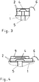
- a pressure sensor component of a first embodiment essentially consists of a first trough-shaped housing part 1 with conductor tracks 3 and a pressure sensor element 2.
- the Fig. 1 shows the pressure sensor device in a plan view.
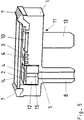
- This support surface is part of the bottom region of the housing part 1 and has an opening 5 for the pressure sensor element 2, so that the medium reaches the pressure sensor element 2 via the opening 5 in the bottom region of the housing part 1 can (representation in the Fig. 3 ).
- the opening 5 is provided with a connection fitting 8, which is at the same time a component of the first housing part 1 (illustration in FIG Fig. 2 ).
- the pressure sensor element 2 is a chip of silicon with a thinned region as the membrane 4.
- the membrane 4 is provided with at least one element as a semiconductor element in the form of a semiconductor resistor, wherein upon expansion, a proportional electrical resistance change occurs.
- the element is part of a known measuring bridge, wherein an electrical resistance change, for example, causes a proportional electrical voltage change.
- the element with contacts of the chip as a pressure sensor element 2 is electrically connected.
- the chip as a pressure sensor element 2 is located on a pedestal and / or a pedestal whose cross section is equal to, smaller or larger than that of the chip as a pressure sensor element 2.
- the base and / or the pedestal has a through opening, said opening and the opening 5 of the housing part 1 enclose a cavity.
- the cross sections of the thinned region as membrane 4 is larger (shown in FIG Fig.
- the contacts of the chip as a pressure sensor element 2 are connected via bonded wire bridges 6 with leading conductors 3 as connection contacts 7 of the pressure sensor component.
- a body preferably as a hardened potting compound, or a second plate-shaped housing part 14 in the first housing part 1, wherein the wall of the first housing part 1 projects beyond the body or the second housing part 14.
- a pressure sensor component essentially consists of a first trough-shaped housing part 1 as circuit carrier with a pressure sensor element 2 and a chip 10 and / or at least one electronic component and a second plate-shaped housing part 14 in a second exemplary embodiment.
- the Fig. 5 shows the pressure sensor component in a sectional view.
- This support surface is part of the bottom region of the first housing part 1 and has a first opening 5 for the pressure sensor element 2, so that the medium via the first opening 5 in the bottom region of the first housing part 1 can get to the pressure sensor element 2.
- the first housing part 1 has in the bottom area a second opening 11 adjacent to the support surfaces for the pressure sensor element 2 and the chip 10 with an evaluation.
- the first opening 5 and the second opening 11 are provided with connection fittings 8, 13, which are at the same time a component of the first housing part 1.
- the pressure sensor element 2 is a chip of silicon with a thinned region as the membrane 4.
- the membrane 4 is provided with at least one element as a semiconductor element in the form of a semiconductor resistor, wherein upon expansion, a proportional electrical resistance change occurs.
- the element is part of a known measuring bridge, wherein an electrical resistance change, for example, causes a proportional electrical voltage change.
- the element with contacts of the chip as a pressure sensor element 2 is electrically connected.
- the chip as a pressure sensor element 2 is located on a base 3 whose cross section is equal to or smaller than that of the chip as a pressure sensor element 2.
- the base 12 may either be a body or consist of several interconnected bodies.
- the support surface may be the surface of a pedestal for the pressure sensor element 2, which is at the same time a component of the first housing part 1.
- the base 12 and / or the pedestal has a through opening 15, said opening 15 and the first opening 5 of the first housing part 1 enclose a cavity.
- the cross sections of the thinned region as membrane 4 is larger (shown in FIG Fig. 3 ), equal to or smaller than that of the openings 5, 15.
- the chip as a pressure sensor element 2 and the chip 10 with an integrated circuit are arranged side by side in the first housing part 1 so that the surfaces of the chip as a pressure sensor element 2 and the chip 10 with an integrated circuit are in a plane (shown in FIG Fig. 5 ).
- other electronic components can be placed in the first housing part 1.
- the contacts of the chip as pressure sensor element 2 and the chip 10 with an integrated circuit are connected depending on the circuit via bonded wire bridges 6 and interconnects 3 with each other and via bonded wire bridges 6 and outwardly leading interconnects 3 as terminal contacts 7 of the pressure sensor component.
- printed conductors 3 end on the edge surface of the wall of the first housing part 1.
- these printed conductors 3 end on comb-like elevations of the wall of the first housing part 1 or are guided over them so that they end on an outer wall area. In one embodiment, these may also be themselves as such elevations be educated. This ensures that these interconnects 3 can be contacted as connecting contacts when placing the pressure sensor component on a printed circuit board with conductor tracks.
- the first housing part 1 is closed with a second plate-shaped housing part 14 such that the second housing part 14 is arranged at a distance from the pressure sensor element 2 and thus at least one cavity which is open via the second opening 11 is present.
- At least the region of the membrane 4 on the side opposite the adjacent medium to be measured can be covered with a hood-like body 9, preferably as a glass body.
- a hood-like body 9 preferably as a glass body.
- the limited by the membrane 4 and this body 9 cavity has a reference volume, in particular with a reference vacuum (representation in the Fig. 4 ). This realizes a pressure sensor component for absolute pressure measurement.
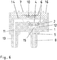
- a pressure sensor component for absolute and / or differential and / or gauge pressure measurement consists in a third embodiment substantially of a first trough-shaped housing part 1 with a pressure sensor element 2 and a second plate-shaped housing part 14 as a circuit carrier with at least one chip 10, for example as an electronic Evaluation circuit and / or at least one electronic component.
- the Fig. 6 shows the pressure sensor component in a sectional view.
- the pressure sensor element 2 connected to printed conductors 3 via bonded wire bridges 6 is located on the carrier surface.
- This carrier surface is at the same time a component of the bottom region of the first Housing part 1 and has a first opening 5 for the pressure sensor element 2, so that the medium can pass through this first opening 5 to the pressure sensor element 2.
- the first housing part 1 has in the bottom region a second opening 11 adjacent to the support surface for the pressure sensor element 2.
- the first opening 5 and the second opening 11 are provided with connection fittings 8, 13, which are at the same time a part of the first housing part 1.
- the pressure sensor element 2 is a chip of silicon with a thinned region as a membrane 4 having at least one element as a semiconductor element on a base 3 corresponding to that of the first embodiment.
- conductor tracks of the first housing part 1 are led to the outside. The end regions are simultaneously formed as connection contacts 7 of this pressure sensor component.
- the first housing part 1 is closed with a second plate-shaped housing part 14 such that the second housing part 14 is arranged at a distance from the pressure sensor element 2 and at least one cavity which is open via the second opening 11 is present. This realizes a pressure sensor component for absolute and / or differential and / or gauge pressure measurement.
- conductor tracks are led to the end regions of the first housing part 1.
- the first housing part 1 is closed with a second plate-shaped housing part 14 such that between the pressure sensor element 2 and the second housing part 14 there is at least one cavity open via the second opening 11.
- the second housing part 14 is formed as a circuit carrier.
- at least one chip 10 with an integrated circuit and / or at least one electronic component and conductor tracks are arranged on the second housing part 14.
- Conductor tracks of the second housing part 14 are connected via edge regions with conductor tracks of the first housing part 1. Further interconnects terminate on the second housing part 14. End regions are simultaneously formed as contacts 7 for the pressure sensor component.
- the chip 10 with an integrated circuit, the printed conductors on the second housing part 14 and the bonded wire bridges 6 for electrically connecting the printed conductors to the integrated circuit of the chip 10 and / or the at least one electronic component are embedded in a potting compound 16.
- a pressure sensor component shows the Fig. 6 ,
- At least the region of the membrane 4 on the side opposite the adjacent and to be measured medium can be covered with a hood-like body 9, in particular as a glass body.
- a hood-like body 9 in particular as a glass body.
- the limited by the membrane 4 and this body 9 cavity has a reference volume advantageously enough with a reference vacuum (shown in the Fig. 4 ). This realizes a pressure sensor component for absolute pressure measurement.
- TAB tape automated bonding
- a body, a medium or a reference vacuum can be located between the pressure sensor element 2 and the second housing part 14.
- the medium may advantageously be a gel and the body made of an elastic material.
- At least one corner region of walls of the first housing part 1 of the pressure sensor component can have an increase.
- This increase is located on adjacent walls and advantageously constitutes an assembly aid and / or a mechanical fastening possibility for the pressure sensor component.
- this elevation is a pin, a hook or a part with a clamping mechanism.
- This increase can thus be easily inserted and fixed in an opening of a support for the pressure sensor component.
- the increase for example, a conical pin with at least one circumferential recess and / or increase, so that in conjunction with the opening and the support of the pressure sensor component, a snap mechanism is realized.
Description
Die Erfindung betrifft Drucksensor-Bauelemente.The invention relates to pressure sensor components.
Durch die Druckschriften
Die Druckschrift
Die Lösungen in den Druckschriften
The publication
The solutions in the pamphlets
Diese Aufgabe wird mit den im Patentanspruch 1 aufgeführten Merkmalen gelöst.This object is achieved with the features listed in
Die Drucksensor-Bauelemente zeichnen sich insbesondere durch eine einfache und kompakte Realisierung bei universeller Einsatzmöglichkeit aus.
Ein erstes wannenförmiges Gehäuseteil als Träger von Leiterbahnen und des Drucksensorelementes ist vorteilhafterweise ein MID-Gehäuseteil (MID = molded interconnect device), so dass dieses Gehäuseteil selbst ein Schaltungsträger ist. Das erste Gehäuseteil besitzt wenigstens eine Trägerfläche, auf dem sich das wenigstens eine Drucksensorelement befindet. Vorteilhafterweise ist die Trägerfläche gleichzeitig ein Bestandteil des ersten Gehäuseteils.
Die ein Bestandteil des ersten Gehäuseteils darstellende Trägerfläche weist wenigstens eine Öffnung für das Drucksensorelement auf, wobei sich die Öffnung im Bodenbereich des ersten Gehäuseteils befindet. Mit einer derartigen Realisierung mit einem Drucksensorelement kann das Drucksensor-Bauelement leicht zur Absolutdruckmessung im Druck zu messenden Medium eingesetzt werden. Das zu messende Medium liegt über die Öffnung an dem Drucksensorelement an.
Die Verwendung eines MID-Gehäuses führt zu einem kompakten Drucksensor-Bauelement, das nur wenige Bestandteile aufweist. Das erste Gehäuseteil führt zu einer leichten Handhabbarkeit und Anschlussmöglichkeit des Drucksensorelementes.
Im ersten Gehäuseteil ist entweder ein zweites plattenförmiges Gehäuseteil oder ein Körper angeordnet, wobei die Wandung des ersten Gehäuseteils das zweite Gehäuseteil oder den Körper überragt und entweder auf der Randfläche der Wandung des ersten Gehäuseteils oder einen Wandbereich umfassende und damit auf einem Außenwandbereich des ersten Gehäuseteils endende Leiterbahnen gleichzeitig Anschlusskontakte sind. Die Endenbereiche sind dami vorteilhafterweise gleichzeitig die elektrischen Kontakte des Drucksensor-Bauelementes nach außen. Diese Endenbereiche und gegebenenfalls weitere vorhandene Endenbereiche von Leiterbahnen können leicht zur elektrischen Kontaktierung und/oder mechanischen Befestigung des Drucksensor-Bauelements zum Beispiel auf Bauelementeträgern genutzt werden, so dass das Drucksensor-Bauelement maschinell auf Bauelementeträger platziert und mit diesem kontaktiert werden kann.
Der Körper im ersten Gehäuseteil ist zum Beispiel eine Vergussmasse zum Schutz des Drucksensorelementes einschließlich dessen Kontaktierung im ersten Gehäuseteil.
Das Gehäuseteil als MID-Gehäuse zeichnet sich weiterhin dadurch aus, dass es als Kunststoffspritzteil leicht und ökonomisch auch in großen Stückzahlen als Massenprodukt herstellbar ist. Dieser Spritzgusskörper wird mit einer strukturierten Metallisierung mit Leiterbahnen versehen, so dass das Gehäuseteil selbst ein Schaltungsträger ist. Dazu wird der Spritzgusskörper mit einer bekannten Metallabscheidung beschichtet, wobei unterschiedliche Eigenschaften der verwendeten Kunststoffe eine selektive Metallisierung bewirken und das strukturierte Leiterbild entsteht. Damit kann das Drucksensor-Bauelement leicht auch als Massenprodukt hergestellt und bereitgestellt werden.
Durch den einfachen Aufbau eignet sich der derartige Aufbau sowohl für eine manuelle Kleinserienfertigung als auch für eine maschinelle Großserienfertigung. Im letzteren Fall kann auch eine Fertigungsstraße mit Bestückungsplätzen und Montageplätzen eingesetzt werden.The pressure sensor components are characterized in particular by a simple and compact realization with universal application possibility.
A first trough-shaped housing part as a carrier of printed conductors and of the pressure sensor element is advantageously an MID housing part (MID = molded interconnect device), so that this housing part itself is a circuit carrier. The first housing part has at least one support surface on which the at least one pressure sensor element is located. Advantageously, the support surface is at the same time a component of the first housing part.
The carrier surface forming part of the first housing part has at least one opening for the pressure sensor element, wherein the opening is located in the bottom area of the first housing part. With such a realization with a pressure sensor element, the pressure sensor component can be easily used for absolute pressure measurement in the medium to be measured. The medium to be measured abuts the pressure sensor element via the opening.
The use of an MID housing results in a compact pressure sensor device that has few components. The first housing part leads to easy handling and connectivity of the pressure sensor element.
In the first housing part either a second plate-shaped housing part or a body is arranged, wherein the wall of the first housing part projects beyond the second housing part or the body and either on the edge surface of the wall of the first Housing part or a wall area comprehensive and thus on an outer wall portion of the first housing part terminating conductor tracks are simultaneously terminal contacts. The end regions are advantageously simultaneously the electrical contacts of the pressure sensor component to the outside. These end regions and, if appropriate, further existing end regions of printed conductors can easily be used for electrical contacting and / or mechanical fastening of the pressure sensor component, for example on component carriers, so that the pressure sensor component can be mechanically placed on component carriers and contacted with same.
The body in the first housing part is, for example, a potting compound for protecting the pressure sensor element including its contacting in the first housing part.
The housing part as an MID housing is further distinguished by the fact that it can be produced as a plastic injection molded part easily and economically even in large quantities as a mass product. This injection molded body is provided with a structured metallization with conductor tracks, so that the housing part itself is a circuit carrier. For this purpose, the injection-molded body is coated with a known metal deposition, with different properties of the plastics used to effect a selective metallization and the structured pattern is formed. Thus, the pressure sensor device can be easily manufactured and provided as a mass product.
Due to the simple structure, such a structure is suitable both for a manual small batch production as well as for a machine mass production. In the latter case, a production line with assembly stations and assembly stations can be used.
Vorteilhafte Ausgestaltungen der Erfindung sind in den Patentansprüchen 2 bis 11 angegeben.Advantageous embodiments of the invention are specified in the
Nach der Weiterbildung des Patentanspruchs 2 weist die ein Bestandteil des ersten Gehäuseteils darstellende Trägerfläche eine erste Öffnung für das Drucksensorelement und das erste Gehäuseteil mindestens eine zweite Öffnung neben der Trägerfläche auf, wobei sich die Öffnungen im Bodenbereich des ersten Gehäuseteils befinden. Weiterhin ist das zweite plattenförmige Gehäuseteil im ersten Gehäuseteil angeordnet, wobei die Wandung des ersten Gehäuseteils das zweite Gehäuseteil überragt, zwischen Drucksensorelement und zweitem Gehäuseteil wenigstens ein über die zweite Öffnung offener Hohlraum vorhanden ist und entweder auf der Randfläche der Wandung des ersten Gehäuseteils oder einen Wandbereich umfassende und damit auf einem Außenwandbereich des ersten Gehäuseteils endende Leiterbahnen gleichzeitig Anschlusskontakte sind.
Damit ist eine einfache und kompakte Realisierung bei universeller Einsatzmöglichkeit vorhanden. So sind diese vorteilhafterweise zur Absolut- und/oder Differenz- und/oder Relativdruckmessung geeignet.
Das erste Gehäuseteil ist mit einem zweiten plattenförmigen Gehäuseteil so versehen, dass das zweite Gehäuseteil beabstandet zu dem Drucksensorelement angeordnet ist. Mit einer derartigen Realisierung mit einem Drucksensorelement kann das Drucksensor-Bauelement vorteilhafterweise leicht entweder zur Absolutdruckmessung oder zur Differenzdruckmessung eingesetzt werden. Bei der ersten Variante ist das erste Gehäuseteil abgeschlossen, wobei das zu messende Medium über die Öffnung an dem Drucksensorelement anliegt. Bei der Differenzdruckmessung als zweite Variante wird das erste Gehäuseteil so mit dem zweiten Gehäuseteil versehen, dass zwei Medien an dem Drucksensorelement angreifen. Das erste Medium kann über die Öffnung auf eine Seite des Drucksensorelementes angreifen, während das zweite Medium über wenigstens eine Öffnung zum Beispiel als Aussparung oder Durchbruch des zweiten Gehäuseteils und den durch den Abstand vorhandene Hohlraum zwischen erstem Gehäuseteil und Drucksensorelement an die andere Seite des Drucksensorelementes gelangt. Dadurch kann eine Gehäuseausführung leicht für sehr unterschiedliche Anwendungen eingesetzt werden, so dass ein universeller Einsatz gegeben ist.According to the embodiment of
This is a simple and compact implementation with universal use available. Thus, these are advantageously suitable for absolute and / or differential and / or relative pressure measurement.
The first housing part is provided with a second plate-shaped housing part such that the second housing part is arranged at a distance from the pressure sensor element. With such a realization with a pressure sensor element, the pressure sensor component can advantageously be easily used either for absolute pressure measurement or for differential pressure measurement. In the first variant, the first housing part is completed, wherein the medium to be measured rests on the pressure sensor element via the opening. In the differential pressure measurement as a second variant, the first housing part is provided with the second housing part such that two media engage the pressure sensor element. The first medium can attack via the opening on one side of the pressure sensor element, while the second medium passes through at least one opening, for example as a recess or opening of the second housing part and the cavity present through the gap between the first housing part and pressure sensor element to the other side of the pressure sensor element , As a result, a housing design can be easily used for very different applications, so that a universal use is given.
Die Leiterbahnen enden nach der Weiterbildung des Patentanspruchs 3 auf kammartigen Erhöhungen der Wandung des Gehäuseteils, so dass eine leichte maschinelle elektrische Kontaktierung in Form von Lotverbindungen des Drucksensor-Bauelements möglich ist. Die Erhöhungen führen vorteilhafterweise dazu, dass benachbarte Leiterbahnen bei dieser Kontaktierung nicht miteinander verbunden werden. Damit können die bekannten und technologisch ausgereiften Verfahren der SMT-Techniken (SMT = surface mounted technology) zur Montage, Befestigung und Kontaktierung des Drucksensor-Bauelementes zur Anwendung kommen.The interconnects end according to the embodiment of
Ein Anschlussfitting für die Öffnung oder mehrere Anschlussfittings für die Öffnungen nach der Weiterbildung des Patentanspruchs 4 gewährleistet oder gewährleisten eine leichte Handhabbarkeit des Drucksensor-Bauelements hinsichtlich des Anschlusses des Mediums. Eine Schlauchleitung kann leicht aufgeschoben werden, wobei auch wenigstens eine Befestigungsschelle für die Schlauchleitung angewandt werden kann. Ein Anschlussfitting gewährleistet einen festen und sicheren Halt der Schlauchleitung.A connection fitting for the opening or a plurality of connection fittings for the openings according to the embodiment of
Das zweite Gehäuseteil ist nach der Weiterbildung des Patentanspruchs 5 ein Bauelementeträger mit Leiterbahnen und damit selbst ein Schaltungsträger. Dadurch sind spezielle und anwenderspezifische Schaltungsvarianten zur Auswertung der erfassten Messwerte realisierbar. Die Gehäuseteile können dabei leicht so ausgebildet sein, dass bei der Verbindung dieser Teile gleichzeitig entsprechend angeordnete Leiterbahnen miteinander elektrisch leitend zusammengeschaltet werden.The second housing part is according to the embodiment of
Wenigstens ein Bauelementeträger mit Leiterbahnen und wenigstens einem Chip mit einer integrierten Schaltung und/oder mindestens einem elektronischen Bauelement und damit ein Schaltungsträger ist nach der Weiterbildung des Patentanspruchs 6 zwischen dem Boden des ersten Gehäuseteils und dem zweiten Gehäuseteil angeordnet und mit Leiterbahnen von Wandbereichen des ersten Gehäuseteils verbunden. Damit ist ein Schichtaufbau gegeben, wodurch komplexe und umfangreiche Schaltungen im Drucksensor-Bauelement realisiert werden können. Die Bauelementeträger können anwenderspezifisch ausgebildet werden, wobei die unterschiedlichsten Schaltungsvarianten realisierbar sind.At least one component carrier with conductor tracks and at least one chip with an integrated circuit and / or at least one electronic component and thus a circuit carrier is arranged according to the embodiment of
Im ersten Gehäuseteil ist nach der Weiterbildung des Patentanspruchs 7 weiterhin wenigstens ein Chip mit einer integrierten Schaltung angeordnet und mit Leiterbahnen dieses Gehäuseteils verbunden. Die integrierte Schaltung ist vorteilhafterweise ein Datenverarbeitungssystem, so dass die Messdaten im Drucksensor-Bauelement aufbereitet werden können. Dadurch ist ein intelligentes Drucksensor-Bauelement realisiert. Ein derartiges Bauelement kann damit auch anwendungsspezifisch hergestellt werden. Dazu sind diese weiterhin nebeneinander entweder in einer Ebene oder in unterschiedlichen Ebenen im ersten Gehäuseteil angeordnet. Das führt zu einer leichten und ökonomischen Herstellung des Drucksensor-Bauelementes.
Dabei können sich die Oberflächen des Chip als Drucksensorelement und des Chip mit einer integrierten Schaltung vorteilhafterweise in einer Ebene befinden. Die Verbindung des jeweiligen Chip mit Leiterbahnen erfolgt vorzugsweise mittels gebondeter Drahtbrücken. Die gleiche Ebene führt zu gleichen technologischen Bearbeitungsbedingungen, so dass eine ökonomische Herstellung gegeben ist.
Damit ist ein intelligentes Drucksensor-Bauelement vorhanden. Durch einen spezifischen Einsatz von speziellen sowohl Drucksensorelementen als auch elektronischen Bauelementen und/oder Schaltungsträgern zum Beispiel als Chip mit einer integrierten Schaltung in Form einer Auswerteschaltung können leicht die unterschiedlichsten Anwendungen realisiert werden.In the first housing part is further arranged according to the embodiment of
In this case, the surfaces of the chip as a pressure sensor element and the chip with an integrated circuit can advantageously be in one plane. The connection of the respective chip with conductor tracks preferably takes place by means of bonded wire bridges. The same level leads to the same technological processing conditions, so that an economic production is given.
This provides an intelligent pressure sensor component. By a specific use of special pressure sensor elements as well as electronic components and / or circuit carriers, for example, as a chip with an integrated circuit in the form of an evaluation circuit, a wide variety of applications can be easily realized.
Nach der Weiterbildung des Patentanspruchs 8 befindet sich zwischen Drucksensorelement und zweitem Gehäuseteil ein Hohlraum, ein Körper, ein Medium oder ein Referenzvakuum. Der Hohlraum, der Körper, das Medium oder das Vakuum sind eine Referenz des Drucksensor-Bauelements. Der Körper befindet sich dazu im Hohlraum zwischen Drucksensorelement und zweitem Gehäuseteil.According to the embodiment of
Wenigstens ein Eckbereich von Wandungen des ersten Gehäuseteils des Drucksensor-Bauelements weist nach der Weiterbildung des Patentanspruchs 9 eine Erhöhung auf. Diese Erhöhung befindet sich auf aneinander grenzenden Wandungen und stellt vorteilhafterweise eine Montagehilfe und/oder eine mechanische Befestigungsmöglichkeit für das Drucksensor-Bauelement dar. Diese Erhöhung ist vorteilhafterweise ein Zapfen, ein Haken oder ein Teil mit einem Klemmmechanismus.At least one corner region of walls of the first housing part of the pressure sensor component has according to the embodiment of
Das Drucksensorelement ist nach der Weiterbildung des Patentanspruchs 10 ein Chip mit einem abgedünnten Bereich als Membran auf einem Sockel. Die Membran weist wenigstens ein elektrisches bei Dehnung seinen elektrischen Widerstandswert ändernden Element auf. Der Sockel besitzt eine durchgehende Öffnung. Diese Öffnung und die Öffnung im ersten Gehäuseteil bewirken, dass das Medium an die Membran des Drucksensorelementes gelangen kann. Die Verwendung eines Sockels erleichtert die Handhabbarkeit des Drucksensorelementes. Weiterhin können auch unterschiedliche Querschnitte der Membran und der Öffnungen leicht realisiert werden. Der Querschnitt und die Dicke der Membran bestimmen die Empfindlichkeit des Drucksensorelementes. Das Element ist vorteilhafterweise ein Halbleiter-Messelement als integraler Bestandteil des Drucksensorelementes. Mit diesen Merkmalen ist das Drucksensor-Bauelement vorteilhafterweise für eine Absolut- und/oder eine Differenz- und/oder Relativdruckmessung geeignet.The pressure sensor element is according to the embodiment of
Nach der Weiterbildung des Patentanspruchs 11 ist wenigstens der Bereich der Membran auf der dem anliegenden und zu messenden Medium gegenüberliegenden Seite mit einem haubenartigen Körper abgedeckt und der durch die Membran und dem Körper begrenzte Hohlraum weist ein Referenzvolumen auf. Eine derartige Realisierung eignet sich nur für eine Absolutdruckmessung. Vorteilhafterweise befindet sich ein Vakuum in diesem Hohlraum. Der haubenartige Körper schützt gleichzeitig wenigstens den druckempfindlichen Bereich des Drucksensorelementes gegenüber einem anliegenden Medium im Drucksensor-Bauelement. Dadurch ist insbesondere die Membran des Drucksensorelementes vom im Drucksensor-Bauelement sich befindenden Medium getrennt. Das Drucksensor-Bauelement zur Messung des Absolutdruckes kann besonders vorteilhaft zur Druckmessung unter schwierigen Medienbedingungen eingesetzt werden.According to the embodiment of
Ausführungsbeispiele der Erfindung sind in den Zeichnungen jeweils prinzipiell dargestellt und werden im folgenden näher beschrieben.
Es zeigen:
- Fig. 1
- ein Drucksensor-Bauelement in einer Draufsicht,
- Fig. 2
- das Drucksensor-Bauelement in einer Vorderansicht
- Fig. 3
- ein Drucksensorelement für eine Differenz- und/oder Relativdruckmessung,
- Fig. 4
- ein Drucksensorelement für eine Absolutdruckmessung,
- Fig. 5
- ein Drucksensor-Bauelement mit zwei Öffnungen in einer Schnittdarstellung,
- Fig. 6
- ein Drucksensor-Bauelement mit einem weiteren Bauelementeträger in einer Schnittdarstellung.
Show it:
- Fig. 1
- a pressure sensor component in a plan view,
- Fig. 2
- the pressure sensor component in a front view
- Fig. 3
- a pressure sensor element for a differential and / or relative pressure measurement,
- Fig. 4
- a pressure sensor element for an absolute pressure measurement,
- Fig. 5
- a pressure sensor device with two openings in a sectional view,
- Fig. 6
- a pressure sensor component with a further component carrier in a sectional view.
Ein Drucksensor-Bauelement eines ersten Ausführungsbeispiels besteht im Wesentlichen aus einem erstem wannenförmigen Gehäuseteil 1 mit Leiterbahnen 3 und einem Drucksensorelement 2.A pressure sensor component of a first embodiment essentially consists of a first trough-shaped
Die
Das erste wannenförmige Gehäuseteil 1 ist ein spritzgegossenes Kunststoffteil mit sowohl auf-/eingebrachten Leiterbahnen 3 als auch einer Trägerfläche als MID-Gehäuseteil (MID = molded interconnect device). Auf der Trägerfläche befindet sich das mit Leiterbahnen 3 verbundene Drucksensorelement 2. Diese Trägerfläche ist Bestandteil des Bodenbereichs des Gehäuseteils 1 und weist eine Öffnung 5 für das Drucksensorelement 2 auf, so dass das Medium über die Öffnung 5 im Bodenbereich des Gehäuseteils 1 zum Drucksensorelement 2 gelangen kann (Darstellung in der
Das Drucksensorelement 2 ist ein Chip aus Silizium mit einem abgedünnten Bereich als Membran 4. Die Membran 4 ist mit wenigstens einem Element als Halbleiterelement in Form eines Halbleiterwiderstandes versehen, wobei bei Dehnung eine verhältnisgleiche elektrische Widerstandsänderung erfolgt. Das Element ist Bestandteil einer bekannten Messbrücke, wobei eine elektrische Widerstandsänderung zum Beispiel eine verhältnisgleiche elektrische Spannungsänderung hervorruft. Dazu ist das Element mit Kontakten des Chip als Drucksensorelement 2 elektrisch leitend verbunden. Der Chip als Drucksensorelement 2 befindet sich auf einem Sockel und/oder einem Podest, dessen Querschnitt gleich, kleiner oder größer als der des Chip als Drucksensorelement 2 ist. Der Sockel und/oder das Podest besitzt eine durchgehende Öffnung, wobei diese Öffnung und die Öffnung 5 des Gehäuseteils 1 einen Hohlraum umschließen. Die Querschnitte des abgedünnten Bereiches als Membran 4 ist größer (Darstellung in der
Die Kontakte des Chip als Drucksensorelement 2 sind über gebondete Drahtbrücken 6 mit nach außen führende Leiterbahnen 3 als Anschlusskontakte 7 des Drucksensor-Bauelements verbunden. Dazu enden Leiterbahnen 3 auf der Randfläche der Wandung des ersten Gehäuseteils 1 oder umfassen dazu einen Wandbereich. Im letzteren Fall enden die Leiterbahnen 3 auf einem Außenwandbereich. Diese enden auf kammartigen Erhöhungen der Wandung des ersten Gehäuseteils 1. In einer Ausführungsform können diese auch als solche Erhöhungen selbst ausgebildet sein. Damit ist eine elektrische Kontaktierung des Drucksensor-Bauelements auf einer Leiterplatte mit Leiterbahnen leicht möglich. Diese Kontaktierungen und weitere können auch gleichzeitig die Befestigung des Drucksensor-Bauelements sein.
Für den Schutz des Drucksensorelementes 2 und der Drahtbrücken 6 befindet sich ein Körper, vorzugsweise als ausgehärtete Vergussmasse, oder ein zweites plattenförmiges Gehäuseteil 14 im ersten Gehäuseteil 1, wobei die Wandung des ersten Gehäuseteils 1 den Körper oder das zweite Gehäuseteil 14 überragt.The first trough-shaped
The
The contacts of the chip as a
For the protection of the
Ein Drucksensor-Bauelement besteht in einem zweitem Ausführungsbeispiel im Wesentlichen aus einem ersten wannenförmigen Gehäuseteil 1 als Schaltungsträger mit einem Drucksensorelement 2 und einem Chip 10 und/oder wenigstens einem elektronischen Bauelement und einem zweiten plattenförmigen Gehäuseteil 14.A pressure sensor component essentially consists of a first trough-shaped
Die
Das erste wannenförmige Gehäuseteil 1 ist ein spritzgegossenes Kunststoffteil mit sowohl auf-/eingebrachten Leiterbahnen 3 als auch Trägerflächen als MID-Gehäuseteil (MID = molded interconnect device). Auf der ersten Trägerfläche befindet sich das mit Leiterbahnen 3 verbundene Drucksensorelement 2. Diese Trägerfläche ist Bestandteil des Bodenbereichs des ersten Gehäuseteils 1 und weist eine erste Öffnung 5 für das Drucksensorelement 2 auf, so dass das Medium über die erste Öffnung 5 im Bodenbereich des ersten Gehäuseteils 1 zum Drucksensorelement 2 gelangen kann. Das erste Gehäuseteil 1 besitzt im Bodenbereich eine zweite Öffnung 11 neben den Trägerflächen für das Drucksensorelement 2 und den Chip 10 mit einer Auswerteelektronik. Die erste Öffnung 5 und die zweite Öffnung 11 sind mit Anschlussfittings 8, 13 versehen, die gleichzeitig ein Bestandteil des ersten Gehäuseteils 1 sind.
Das Drucksensorelement 2 ist ein Chip aus Silizium mit einem abgedünnten Bereich als Membran 4. Die Membran 4 ist mit wenigstens einem Element als Halbleiterelement in Form eines Halbleiterwiderstandes versehen, wobei bei Dehnung eine verhältnisgleiche elektrische Widerstandsänderung erfolgt. Das Element ist Bestandteil einer bekannten Messbrücke, wobei eine elektrische Widerstandsänderung zum Beispiel eine verhältnisgleiche elektrische Spannungsänderung hervorruft. Dazu ist das Element mit Kontakten des Chip als Drucksensorelement 2 elektrisch leitend verbunden. Der Chip als Drucksensorelement 2 befindet sich auf einem Sockel 3, dessen Querschnitt gleich oder kleiner als der des Chip als Drucksensorelement 2 ist. Der Sockel 12 kann entweder ein Körper sein oder aus mehreren miteinander verbundenen Körpern bestehen. In einer Ausführungsform kann die Trägerfläche die Oberfläche eines Podestes für das Drucksensorelement 2 sein, dass gleichzeitig ein Bestandteil des ersten Gehäuseteils 1 ist. Der Sockel 12 und/oder das Podest besitzt eine durchgehende Öffnung 15, wobei diese Öffnung 15 und die erste Öffnung 5 des ersten Gehäuseteils 1 einen Hohlraum umschließen. Die Querschnitte des abgedünnten Bereiches als Membran 4 ist größer (Darstellung in der
Der Chip als Drucksensorelement 2 und der Chip 10 mit einer integrierten Schaltung sind nebeneinander im ersten Gehäuseteil 1 so angeordnet, dass sich die Oberflächen des Chip als Drucksensorelement 2 und des Chip 10 mit einer integrierten Schaltung in einer Ebene befinden (Darstellung in der
The
The chip as a
In einer Ausführungsform des ersten Ausführungsbeispiels kann wenigstens der Bereich der Membran 4 auf der dem anliegenden und zu messenden Medium gegenüberliegenden Seite mit einem haubenartigen Körper 9 vorzugsweise als Glaskörper abgedeckt sein. Der durch die Membran 4 und diesem Körper 9 begrenzte Hohlraum weist ein Referenzvolumen insbesondere mit einem Referenzvakuum auf (Darstellung in der
Ein Drucksensor-Bauelement zur Absolut- und/oder Differenz- und/oder Relativdruckmessung besteht in einem drittem Ausführungsbeispiel im Wesentlichen aus einem ersten wannenförmigen Gehäuseteil 1 mit einem Drucksensorelement 2 und einem zweiten plattenförmigen Gehäuseteil 14 als Schaltungsträger mit wenigstens einem Chip 10 zum Beispiel als elektronische Auswerteschaltung und/oder mindestens einem elektronischen Bauelement.A pressure sensor component for absolute and / or differential and / or gauge pressure measurement consists in a third embodiment substantially of a first trough-shaped
Die
Das erste wannenförmige Gehäuseteil 1 ist ein spritzgegossenes Kunststoffteil mit sowohl auf-/eingebrachten Leiterbahnen 3 als auch einer Trägerfläche als MID-Gehäuseteil (MID = molded interconnect device). Auf der Trägerfläche befindet sich das mit Leiterbahnen 3 über gebondete Drahtbrücken 6 verbundene Drucksensorelement 2. Diese Trägerfläche ist gleichzeitig ein Bestandteil des Bodenbereiches des ersten Gehäuseteils 1 und weist eine erste Öffnung 5 für das Drucksensorelement 2 auf, so dass das Medium über diese erste Öffnung 5 zum Drucksensorelement 2 gelangen kann. Das erste Gehäuseteil 1 besitzt im Bodenbereich eine zweite Öffnung 11 neben der Trägerfläche für das Drucksensorelement 2. Die erste Öffnung 5 und die zweite Öffnung 11 sind mit Anschlussfittings 8, 13 versehen, die gleichzeitig ein Bestandteil des ersten Gehäuseteils 1 sind.
Das Drucksensorelement 2 ist ein Chip aus Silizium mit einem abgedünnten Bereich als Membran 4 mit wenigstens einem Element als Halbleiterelement auf einem Sockel 3 entsprechend dem des ersten Ausführungsbeispiels.
In einer ersten Ausführungsform des dritten Ausführungsbeispiels sind Leiterbahnen des ersten Gehäuseteils 1 nach außen geführt. Die Endenbereiche sind gleichzeitig als Anschlusskontakte 7 dieses Drucksensor-Bauelementes ausgebildet. Das erste Gehäuseteil 1 ist mit einem zweiten plattenförmigen Gehäuseteil 14 so abgeschlossen, dass das zweite Gehäuseteil 14 beabstandet zu dem Drucksensorelement 2 angeordnet ist und wenigstens ein über die zweite Öffnung 11 offener Hohlraum vorhanden ist. Damit ist ein Drucksensor-Bauelement zur Absolut- und/oder Differenz- und/oder Relativdruckmessung realisiert.
In einer zweiten Ausführungsform des dritten Ausführungsbeispiels sind Leiterbahnen zu den Endenbereichen des ersten Gehäuseteils 1 geführt. Das erste Gehäuseteil 1 ist mit einem zweiten plattenförmigen Gehäuseteil 14 so abgeschlossen, dass zwischen Drucksensorelement 2 und zweitem Gehäuseteil 14 wenigstens ein über die zweite Öffnung 11 offener Hohlraum vorhanden ist. Das zweite Gehäuseteil 14 ist als Schaltungsträger ausgebildet. Dazu ist wenigstens ein Chip 10 mit einer integrierten Schaltung und/oder mindestens ein elektronisches Bauelement und Leiterbahnen auf dem zweiten Gehäuseteil 14 angeordnet. Leiterbahnen des zweiten Gehäuseteils 14 sind über Randbereiche mit Leiterbahnen des ersten Gehäuseteils 1 verbunden. Weitere Leiterbahnen enden auf dem zweiten Gehäuseteil 14. Endenbereiche sind gleichzeitig als Kontakte 7 für das Drucksensor-Bauelement ausgebildet. Der Chip 10 mit einer integrierten Schaltung, die Leiterbahnen auf dem zweiten Gehäuseteil 14 und die gebondeten Drahtbrücken 6 zur elektrischen Verbindung der Leiterbahnen mit der integrierten Schaltung des Chip 10 und/oder des wenigstens einen elektronischen Bauelementes sind in einer Vergussmasse 16 eingebettet. Ein derartiges Drucksensor-Bauelement zeigt die
The
In a first embodiment of the third embodiment, conductor tracks of the
In a second embodiment of the third embodiment, conductor tracks are led to the end regions of the
In einer weiteren Ausführungsform der Ausführungsbeispiele kann wenigstens der Bereich der Membran 4 auf der dem anliegenden und zu messenden Medium gegenüberliegenden Seite mit einem haubenartigen Körper 9 insbesondere als Glaskörper abgedeckt sein. Der durch die Membran 4 und diesem Körper 9 begrenzte Hohlraum weist ein Referenzvolumen vorteil-hafterweise mit einem Referenzvakuum auf (Darstellung in der
Der Chip 10 als Auswerteelektronik und/oder der Chip als Drucksensorelement 2 können in weiteren Ausführungsformen der Ausführungsbeispiele auch mit anderen bekannten Verbindungstechnologien wie zum Beispiel der TAB-Technik (TAB = tape automated Bonding) mit Leiterbahnen der Gehäuseteile 1, 14 verbunden sein.The
In weiteren Ausführungsformen der Ausführungsbeispiele kann sich zwischen Drucksensorelement 2 und zweitem Gehäuseteil 14 ein Körper, ein Medium oder ein Referenzvakuum befinden. Das Medium kann vorteilhafterweise ein Gel sein und der Körper aus einem elastischen Material bestehen.In further embodiments of the exemplary embodiments, a body, a medium or a reference vacuum can be located between the
In weiteren Ausführungsformen der Ausführungsbeispiele kann wenigstens ein Eckbereich von Wandungen des ersten Gehäuseteils 1 des Drucksensor-Bauelementes eine Erhöhung aufweisen. Diese Erhöhung befindet sich auf aneinander grenzenden Wandungen und stellt vorteilhafterweise eine Montagehilfe und/oder eine mechanische Befestigungsmöglichkeit für das Drucksensor-Bauelement dar. Vorteilhafterweise ist diese Erhöhung ein Zapfen, ein Haken oder ein Teil mit einem Klemmmechanismus. Diese Erhöhung kann damit leicht in eine Öffnung eines Trägers für das Drucksensor-Bauelement eingeführt und befestigt werden. Dazu ist die Erhöhung zum Beispiel ein konischer Zapfen mit wenigstens einer umlaufenden Vertiefung und/oder Erhöhung, so dass in Verbindung mit der Öffnung und des Trägers des Drucksensor-Bauelementes ein Schnappmechanismus realisiert ist.In further embodiments of the exemplary embodiments, at least one corner region of walls of the
Claims (6)
- Pressure sensor component for measuring
differential pressure, comprising the following features:- a first tub-shaped housing part (1) as spray-cast plastic part having both conductor tracks (3) as MID (moulded interconnect device) housing part and in the interior at least one support area,- a pressure sensor element (2), connected to conductor tracks (3), as a chip having a thinned area as membrane (4) on a base (12) on the support area, the membrane (4) having at least one element changing its electrical resistance value in the case of an expansion and the element being connected electrically conductively to contacts of the chip as pressure sensor element (2) and the cross section and the thickness of the membrane determining the sensitivity of the pressure sensor component,- a first opening (5) for the pressure sensor element (2) in the support area as a component of the first housing part (1) in connection with a continuous opening (15) in the base (12), the cross sections of the membrane (4) and of the openings (5, 15) being identical or different,- at least one second opening (11) in the first housing part (1) next to the support area, the openings (5, 11) being located in the bottom area of the first housing part (1),- a second plate-shaped housing part (14) in the first housing part (1), the wall of the first housing part (1) protruding over the second housing part (14), between pressure sensor element (2) and second housing part (14), at least one hollow space open over the second opening (11) being present, and- conductor tracks (3) ending on comb-like raised parts of the wall of the first housing part (1) as simultaneous connecting contacts (7), attachments or connecting contacts (7) and attachments. - Pressure sensor component according to Patent Claim 1, characterized in that the first housing part (1)
has connection fittings (8, 13) for the first opening (5) and the second opening (11). - Pressure sensor component according to Patent Claim 1, characterized in that the second housing part (14) is a component carrier with conductor tracks and at least one chip (10) having an integrated circuit and/or at least one electronic component and is thus a circuit carrier.
- Pressure sensor component according to Patent Claim 1, characterized in that at least one component carrier having conductor tracks and at least one chip (10) with an integrated circuit and/or at least one electronic component and thus a circuit carrier is arranged between the bottom of the first housing part (1) and the second housing part (14) and connected to conductor tracks of wall areas of the first housing part (1).
- Pressure sensor component according to Patent Claim 1, characterized in that at least one chip (10) with an integrated circuit is arranged in the first housing part (1) and connected to conductor tracks (3), the chip as pressure sensor element (2) and the chip (10) with an integrated circuit being arranged next to one another either in one plane or in different planes in the first housing part (1).
- Pressure sensor component according to Patent Claim 1, characterized in that at least one corner area of walls of the first housing part (1) has a raised part, the raised part being a cone, a hook or a part having a clamping mechanism.
Applications Claiming Priority (4)
| Application Number | Priority Date | Filing Date | Title |
|---|---|---|---|
| DE102005053876A DE102005053876B4 (en) | 2005-11-09 | 2005-11-09 | Pressure sensor component |
| DE202005017627U DE202005017627U1 (en) | 2005-11-09 | 2005-11-09 | Pressure sensor component has an injection molded plastic housing with an inner support surface, in the form of a molded interconnect device, on which the pressure sensor element is mounted |
| DE202005017626U DE202005017626U1 (en) | 2005-11-09 | 2005-11-09 | Pressure sensor unit with optional intelligence includes pressure injection molded casing with conductive tracks, molded interconnect device support surface and sensor opening |
| DE200510053877 DE102005053877B4 (en) | 2005-11-09 | 2005-11-09 | Pressure sensor component |
Publications (3)
| Publication Number | Publication Date |
|---|---|
| EP1785708A2 EP1785708A2 (en) | 2007-05-16 |
| EP1785708A3 EP1785708A3 (en) | 2009-12-30 |
| EP1785708B1 true EP1785708B1 (en) | 2018-01-03 |
Family
ID=37734824
Family Applications (1)
| Application Number | Title | Priority Date | Filing Date |
|---|---|---|---|
| EP06400035.9A Active EP1785708B1 (en) | 2005-11-09 | 2006-11-07 | Pressure sensor component |
Country Status (1)
| Country | Link |
|---|---|
| EP (1) | EP1785708B1 (en) |
Families Citing this family (5)
| Publication number | Priority date | Publication date | Assignee | Title |
|---|---|---|---|---|
| DE102010003724A1 (en) * | 2010-04-08 | 2011-10-13 | Robert Bosch Gmbh | Pressure sensor assembly |
| US9021689B2 (en) | 2011-06-02 | 2015-05-05 | Freescale Semiconductor, Inc. | Method of making a dual port pressure sensor |
| US8307714B1 (en) * | 2011-06-02 | 2012-11-13 | Freescale Semiconductor, Inc. | Dual port pressure sensor |
| EP2916120A1 (en) * | 2014-03-04 | 2015-09-09 | seleon GmbH | Sensor block, tube and manufacturing method |
| RU2609223C1 (en) * | 2015-10-08 | 2017-01-31 | Акционерное общество "Научно-исследовательский институт Авиационного оборудования" | Strain gauge of absolute pressure based on soi micro-electromechanical system |
Family Cites Families (7)
| Publication number | Priority date | Publication date | Assignee | Title |
|---|---|---|---|---|
| JP3209118B2 (en) * | 1996-05-30 | 2001-09-17 | 松下電工株式会社 | Pressure sensor package body and method of manufacturing the same |
| DE19626084C2 (en) * | 1996-06-28 | 2003-04-17 | Infineon Technologies Ag | Pressure sensor device for mounting on the assembly surface of a printed circuit board |
| JP3209119B2 (en) * | 1996-07-30 | 2001-09-17 | 松下電工株式会社 | Pressure sensor |
| JP2003133453A (en) * | 2001-10-29 | 2003-05-09 | Matsushita Electric Works Ltd | Pressure sensor |
| JP3627693B2 (en) * | 2001-10-29 | 2005-03-09 | 松下電工株式会社 | Pressure sensor |
| JP2003130742A (en) * | 2001-10-29 | 2003-05-08 | Matsushita Electric Works Ltd | Semiconductor pressure sensor |
| JP2003130749A (en) * | 2001-10-29 | 2003-05-08 | Matsushita Electric Works Ltd | Pressure sensor |
-
2006
- 2006-11-07 EP EP06400035.9A patent/EP1785708B1/en active Active
Non-Patent Citations (1)
| Title |
|---|
| None * |
Also Published As
| Publication number | Publication date |
|---|---|
| EP1785708A2 (en) | 2007-05-16 |
| EP1785708A3 (en) | 2009-12-30 |
Similar Documents
| Publication | Publication Date | Title |
|---|---|---|
| DE102014200093A1 (en) | Sensor for detecting a temperature and a pressure of a fluid medium | |
| EP1728060B1 (en) | Sensor module provided with capacitor emc and esd protection | |
| EP1797437B1 (en) | Device for determining electric variables | |
| DE10352917A1 (en) | Sensor arrangement with several potentiometric sensors | |
| EP0935743B1 (en) | Pressure sensor unit, especially for automotive engineering applications | |
| WO1989008243A1 (en) | Manometer | |
| EP1785708B1 (en) | Pressure sensor component | |
| DE10014992A1 (en) | Sensor arrangement for high pressure sensor has electric connections provided between hybrid circuit and sensor circuit and earth connection to housing | |
| DE102014219030B4 (en) | plug module | |
| DE102005053876B4 (en) | Pressure sensor component | |
| DE102014118769B4 (en) | Pressure sensor module with a sensor chip and passive components within a common housing | |
| DE102007000813B4 (en) | With a connector integrated sensor and method of making this | |
| DE102007054717B4 (en) | Transmitter and method of making a transmitter | |
| DE202005017626U1 (en) | Pressure sensor unit with optional intelligence includes pressure injection molded casing with conductive tracks, molded interconnect device support surface and sensor opening | |
| DE102005020345A1 (en) | Sealing structure for a connector | |
| DE102007041785A1 (en) | Semiconductor device and its manufacturing method | |
| DE102013220091A1 (en) | pressure sensor | |
| DE3200448C2 (en) | Method of manufacturing a semiconductor pressure transducer assembly | |
| DE102005053877B4 (en) | Pressure sensor component | |
| EP3942266A1 (en) | Sensor assembly comprising a temperature sensor element, and method for the production of said assembly | |
| EP1353160B1 (en) | Pressure sensor | |
| DE102013223542A1 (en) | Electronic unit with circuit board | |
| DE19902450B4 (en) | Miniaturized electronic system and method suitable for its production | |
| DE202005017627U1 (en) | Pressure sensor component has an injection molded plastic housing with an inner support surface, in the form of a molded interconnect device, on which the pressure sensor element is mounted | |
| DE102017218893A1 (en) | Sensor arrangement for determining at least one parameter of a fluid flowing through a measuring channel |
Legal Events
| Date | Code | Title | Description |
|---|---|---|---|
| PUAI | Public reference made under article 153(3) epc to a published international application that has entered the european phase |
Free format text: ORIGINAL CODE: 0009012 |
|
| AK | Designated contracting states |
Kind code of ref document: A2 Designated state(s): AT BE BG CH CY CZ DE DK EE ES FI FR GB GR HU IE IS IT LI LT LU LV MC NL PL PT RO SE SI SK TR |
|
| AX | Request for extension of the european patent |
Extension state: AL BA HR MK YU |
|
| PUAL | Search report despatched |
Free format text: ORIGINAL CODE: 0009013 |
|
| AK | Designated contracting states |
Kind code of ref document: A3 Designated state(s): AT BE BG CH CY CZ DE DK EE ES FI FR GB GR HU IE IS IT LI LT LU LV MC NL PL PT RO SE SI SK TR |
|
| AX | Request for extension of the european patent |
Extension state: AL BA HR MK RS |
|
| 17P | Request for examination filed |
Effective date: 20100623 |
|
| 17Q | First examination report despatched |
Effective date: 20100721 |
|
| AKX | Designation fees paid |
Designated state(s): AT BE BG CH CY CZ DE DK EE ES FI FR GB GR HU IE IS IT LI LT LU LV MC NL PL PT RO SE SI SK TR |
|
| AXX | Extension fees paid |
Extension state: AL Payment date: 20100623 Extension state: BA Payment date: 20100623 Extension state: RS Payment date: 20100623 |
|
| RAP1 | Party data changed (applicant data changed or rights of an application transferred) |
Owner name: HARTING AG Owner name: AKTIV SENSOR GMBH |
|
| REG | Reference to a national code |
Ref country code: DE Ref legal event code: R079 Ref document number: 502006015770 Country of ref document: DE Free format text: PREVIOUS MAIN CLASS: G01L0009000000 Ipc: G01L0019000000 |
|
| GRAP | Despatch of communication of intention to grant a patent |
Free format text: ORIGINAL CODE: EPIDOSNIGR1 |
|
| STAA | Information on the status of an ep patent application or granted ep patent |
Free format text: STATUS: GRANT OF PATENT IS INTENDED |
|
| RIC1 | Information provided on ipc code assigned before grant |
Ipc: G01L 9/00 20060101ALI20161209BHEP Ipc: G01L 19/14 20060101ALI20161209BHEP Ipc: G01L 19/00 20060101AFI20161209BHEP |
|
| INTG | Intention to grant announced |
Effective date: 20170105 |
|
| RAP1 | Party data changed (applicant data changed or rights of an application transferred) |
Owner name: TDK-EPC AG & CO. KG Owner name: HARTING AG |
|
| GRAS | Grant fee paid |
Free format text: ORIGINAL CODE: EPIDOSNIGR3 |
|
| GRAJ | Information related to disapproval of communication of intention to grant by the applicant or resumption of examination proceedings by the epo deleted |
Free format text: ORIGINAL CODE: EPIDOSDIGR1 |
|
| GRAL | Information related to payment of fee for publishing/printing deleted |
Free format text: ORIGINAL CODE: EPIDOSDIGR3 |
|
| STAA | Information on the status of an ep patent application or granted ep patent |
Free format text: STATUS: EXAMINATION IS IN PROGRESS |
|
| GRAJ | Information related to disapproval of communication of intention to grant by the applicant or resumption of examination proceedings by the epo deleted |
Free format text: ORIGINAL CODE: EPIDOSDIGR1 |
|
| GRAL | Information related to payment of fee for publishing/printing deleted |
Free format text: ORIGINAL CODE: EPIDOSDIGR3 |
|
| INTC | Intention to grant announced (deleted) | ||
| INTC | Intention to grant announced (deleted) | ||
| GRAR | Information related to intention to grant a patent recorded |
Free format text: ORIGINAL CODE: EPIDOSNIGR71 |
|
| STAA | Information on the status of an ep patent application or granted ep patent |
Free format text: STATUS: GRANT OF PATENT IS INTENDED |
|
| INTG | Intention to grant announced |
Effective date: 20171026 |
|
| GRAA | (expected) grant |
Free format text: ORIGINAL CODE: 0009210 |
|
| STAA | Information on the status of an ep patent application or granted ep patent |
Free format text: STATUS: THE PATENT HAS BEEN GRANTED |
|
| REG | Reference to a national code |
Ref country code: DE Ref legal event code: R081 Ref document number: 502006015770 Country of ref document: DE Owner name: HARTING AG, CH Free format text: FORMER OWNERS: AKTIV-SENSOR GMBH, 14532 STAHNSDORF, DE; HARTING MITRONICS AG, BIEL, CH Ref country code: DE Ref legal event code: R081 Ref document number: 502006015770 Country of ref document: DE Owner name: TDK ELECTRONICS AG, DE Free format text: FORMER OWNERS: AKTIV-SENSOR GMBH, 14532 STAHNSDORF, DE; HARTING MITRONICS AG, BIEL, CH |
|
| AK | Designated contracting states |
Kind code of ref document: B1 Designated state(s): AT BE BG CH CY CZ DE DK EE ES FI FR GB GR HU IE IS IT LI LT LU LV MC NL PL PT RO SE SI SK TR |
|
| AX | Request for extension of the european patent |
Extension state: AL BA RS |
|
| REG | Reference to a national code |
Ref country code: GB Ref legal event code: FG4D Free format text: NOT ENGLISH |
|
| REG | Reference to a national code |
Ref country code: CH Ref legal event code: EP Ref country code: AT Ref legal event code: REF Ref document number: 960736 Country of ref document: AT Kind code of ref document: T Effective date: 20180115 |
|
| REG | Reference to a national code |
Ref country code: IE Ref legal event code: FG4D Free format text: LANGUAGE OF EP DOCUMENT: GERMAN |
|
| REG | Reference to a national code |
Ref country code: DE Ref legal event code: R096 Ref document number: 502006015770 Country of ref document: DE |
|
| REG | Reference to a national code |
Ref country code: NL Ref legal event code: MP Effective date: 20180103 |
|
| REG | Reference to a national code |
Ref country code: LT Ref legal event code: MG4D |
|
| PG25 | Lapsed in a contracting state [announced via postgrant information from national office to epo] |
Ref country code: NL Free format text: LAPSE BECAUSE OF FAILURE TO SUBMIT A TRANSLATION OF THE DESCRIPTION OR TO PAY THE FEE WITHIN THE PRESCRIBED TIME-LIMIT Effective date: 20180103 |
|
| PG25 | Lapsed in a contracting state [announced via postgrant information from national office to epo] |
Ref country code: FI Free format text: LAPSE BECAUSE OF FAILURE TO SUBMIT A TRANSLATION OF THE DESCRIPTION OR TO PAY THE FEE WITHIN THE PRESCRIBED TIME-LIMIT Effective date: 20180103 Ref country code: LT Free format text: LAPSE BECAUSE OF FAILURE TO SUBMIT A TRANSLATION OF THE DESCRIPTION OR TO PAY THE FEE WITHIN THE PRESCRIBED TIME-LIMIT Effective date: 20180103 Ref country code: CY Free format text: LAPSE BECAUSE OF FAILURE TO SUBMIT A TRANSLATION OF THE DESCRIPTION OR TO PAY THE FEE WITHIN THE PRESCRIBED TIME-LIMIT Effective date: 20180103 Ref country code: ES Free format text: LAPSE BECAUSE OF FAILURE TO SUBMIT A TRANSLATION OF THE DESCRIPTION OR TO PAY THE FEE WITHIN THE PRESCRIBED TIME-LIMIT Effective date: 20180103 |
|
| PG25 | Lapsed in a contracting state [announced via postgrant information from national office to epo] |
Ref country code: GR Free format text: LAPSE BECAUSE OF FAILURE TO SUBMIT A TRANSLATION OF THE DESCRIPTION OR TO PAY THE FEE WITHIN THE PRESCRIBED TIME-LIMIT Effective date: 20180404 Ref country code: PL Free format text: LAPSE BECAUSE OF FAILURE TO SUBMIT A TRANSLATION OF THE DESCRIPTION OR TO PAY THE FEE WITHIN THE PRESCRIBED TIME-LIMIT Effective date: 20180103 Ref country code: BG Free format text: LAPSE BECAUSE OF FAILURE TO SUBMIT A TRANSLATION OF THE DESCRIPTION OR TO PAY THE FEE WITHIN THE PRESCRIBED TIME-LIMIT Effective date: 20180403 Ref country code: LV Free format text: LAPSE BECAUSE OF FAILURE TO SUBMIT A TRANSLATION OF THE DESCRIPTION OR TO PAY THE FEE WITHIN THE PRESCRIBED TIME-LIMIT Effective date: 20180103 Ref country code: IS Free format text: LAPSE BECAUSE OF FAILURE TO SUBMIT A TRANSLATION OF THE DESCRIPTION OR TO PAY THE FEE WITHIN THE PRESCRIBED TIME-LIMIT Effective date: 20180503 Ref country code: SE Free format text: LAPSE BECAUSE OF FAILURE TO SUBMIT A TRANSLATION OF THE DESCRIPTION OR TO PAY THE FEE WITHIN THE PRESCRIBED TIME-LIMIT Effective date: 20180103 |
|
| REG | Reference to a national code |
Ref country code: DE Ref legal event code: R097 Ref document number: 502006015770 Country of ref document: DE |
|
| PG25 | Lapsed in a contracting state [announced via postgrant information from national office to epo] |
Ref country code: IT Free format text: LAPSE BECAUSE OF FAILURE TO SUBMIT A TRANSLATION OF THE DESCRIPTION OR TO PAY THE FEE WITHIN THE PRESCRIBED TIME-LIMIT Effective date: 20180103 Ref country code: RO Free format text: LAPSE BECAUSE OF FAILURE TO SUBMIT A TRANSLATION OF THE DESCRIPTION OR TO PAY THE FEE WITHIN THE PRESCRIBED TIME-LIMIT Effective date: 20180103 Ref country code: EE Free format text: LAPSE BECAUSE OF FAILURE TO SUBMIT A TRANSLATION OF THE DESCRIPTION OR TO PAY THE FEE WITHIN THE PRESCRIBED TIME-LIMIT Effective date: 20180103 |
|
| PLBE | No opposition filed within time limit |
Free format text: ORIGINAL CODE: 0009261 |
|
| STAA | Information on the status of an ep patent application or granted ep patent |
Free format text: STATUS: NO OPPOSITION FILED WITHIN TIME LIMIT |
|
| PG25 | Lapsed in a contracting state [announced via postgrant information from national office to epo] |
Ref country code: CZ Free format text: LAPSE BECAUSE OF FAILURE TO SUBMIT A TRANSLATION OF THE DESCRIPTION OR TO PAY THE FEE WITHIN THE PRESCRIBED TIME-LIMIT Effective date: 20180103 Ref country code: SK Free format text: LAPSE BECAUSE OF FAILURE TO SUBMIT A TRANSLATION OF THE DESCRIPTION OR TO PAY THE FEE WITHIN THE PRESCRIBED TIME-LIMIT Effective date: 20180103 Ref country code: DK Free format text: LAPSE BECAUSE OF FAILURE TO SUBMIT A TRANSLATION OF THE DESCRIPTION OR TO PAY THE FEE WITHIN THE PRESCRIBED TIME-LIMIT Effective date: 20180103 |
|
| 26N | No opposition filed |
Effective date: 20181005 |
|
| PG25 | Lapsed in a contracting state [announced via postgrant information from national office to epo] |
Ref country code: SI Free format text: LAPSE BECAUSE OF FAILURE TO SUBMIT A TRANSLATION OF THE DESCRIPTION OR TO PAY THE FEE WITHIN THE PRESCRIBED TIME-LIMIT Effective date: 20180103 |
|
| REG | Reference to a national code |
Ref country code: CH Ref legal event code: PL |
|
| GBPC | Gb: european patent ceased through non-payment of renewal fee |
Effective date: 20181107 |
|
| PG25 | Lapsed in a contracting state [announced via postgrant information from national office to epo] |
Ref country code: MC Free format text: LAPSE BECAUSE OF FAILURE TO SUBMIT A TRANSLATION OF THE DESCRIPTION OR TO PAY THE FEE WITHIN THE PRESCRIBED TIME-LIMIT Effective date: 20180103 Ref country code: LU Free format text: LAPSE BECAUSE OF NON-PAYMENT OF DUE FEES Effective date: 20181107 |
|
| REG | Reference to a national code |
Ref country code: BE Ref legal event code: MM Effective date: 20181130 |
|
| REG | Reference to a national code |
Ref country code: IE Ref legal event code: MM4A |
|
| PG25 | Lapsed in a contracting state [announced via postgrant information from national office to epo] |
Ref country code: CH Free format text: LAPSE BECAUSE OF NON-PAYMENT OF DUE FEES Effective date: 20181130 Ref country code: LI Free format text: LAPSE BECAUSE OF NON-PAYMENT OF DUE FEES Effective date: 20181130 |
|
| PG25 | Lapsed in a contracting state [announced via postgrant information from national office to epo] |
Ref country code: IE Free format text: LAPSE BECAUSE OF NON-PAYMENT OF DUE FEES Effective date: 20181107 Ref country code: FR Free format text: LAPSE BECAUSE OF NON-PAYMENT OF DUE FEES Effective date: 20181130 |
|
| PG25 | Lapsed in a contracting state [announced via postgrant information from national office to epo] |
Ref country code: BE Free format text: LAPSE BECAUSE OF NON-PAYMENT OF DUE FEES Effective date: 20181130 |
|
| PG25 | Lapsed in a contracting state [announced via postgrant information from national office to epo] |
Ref country code: GB Free format text: LAPSE BECAUSE OF NON-PAYMENT OF DUE FEES Effective date: 20181107 |
|
| REG | Reference to a national code |
Ref country code: AT Ref legal event code: MM01 Ref document number: 960736 Country of ref document: AT Kind code of ref document: T Effective date: 20181107 |
|
| PG25 | Lapsed in a contracting state [announced via postgrant information from national office to epo] |
Ref country code: AT Free format text: LAPSE BECAUSE OF NON-PAYMENT OF DUE FEES Effective date: 20181107 |
|
| PG25 | Lapsed in a contracting state [announced via postgrant information from national office to epo] |
Ref country code: TR Free format text: LAPSE BECAUSE OF FAILURE TO SUBMIT A TRANSLATION OF THE DESCRIPTION OR TO PAY THE FEE WITHIN THE PRESCRIBED TIME-LIMIT Effective date: 20180103 |
|
| PG25 | Lapsed in a contracting state [announced via postgrant information from national office to epo] |
Ref country code: PT Free format text: LAPSE BECAUSE OF FAILURE TO SUBMIT A TRANSLATION OF THE DESCRIPTION OR TO PAY THE FEE WITHIN THE PRESCRIBED TIME-LIMIT Effective date: 20180103 |
|
| PG25 | Lapsed in a contracting state [announced via postgrant information from national office to epo] |
Ref country code: HU Free format text: LAPSE BECAUSE OF FAILURE TO SUBMIT A TRANSLATION OF THE DESCRIPTION OR TO PAY THE FEE WITHIN THE PRESCRIBED TIME-LIMIT; INVALID AB INITIO Effective date: 20061107 |
|
| REG | Reference to a national code |
Ref country code: DE Ref legal event code: R082 Ref document number: 502006015770 Country of ref document: DE Representative=s name: EPPING HERMANN FISCHER PATENTANWALTSGESELLSCHA, DE Ref country code: DE Ref legal event code: R081 Ref document number: 502006015770 Country of ref document: DE Owner name: HARTING AG, CH Free format text: FORMER OWNERS: HARTING AG, BIEL, CH; TDK-EPC AG & CO. KG, 14532 STAHNSDORF, DE Ref country code: DE Ref legal event code: R081 Ref document number: 502006015770 Country of ref document: DE Owner name: TDK ELECTRONICS AG, DE Free format text: FORMER OWNERS: HARTING AG, BIEL, CH; TDK-EPC AG & CO. KG, 14532 STAHNSDORF, DE |
|
| REG | Reference to a national code |
Ref country code: DE Ref legal event code: R082 Ref document number: 502006015770 Country of ref document: DE Representative=s name: EPPING HERMANN FISCHER PATENTANWALTSGESELLSCHA, DE Ref country code: DE Ref legal event code: R081 Ref document number: 502006015770 Country of ref document: DE Owner name: HARTING AG, CH Free format text: FORMER OWNERS: HARTING AG, BIEL, CH; TDK SENSORS AG & CO. KG, 14167 BERLIN, DE Ref country code: DE Ref legal event code: R081 Ref document number: 502006015770 Country of ref document: DE Owner name: TDK ELECTRONICS AG, DE Free format text: FORMER OWNERS: HARTING AG, BIEL, CH; TDK SENSORS AG & CO. KG, 14167 BERLIN, DE |
|
| PGFP | Annual fee paid to national office [announced via postgrant information from national office to epo] |
Ref country code: DE Payment date: 20221122 Year of fee payment: 17 |
|
| P01 | Opt-out of the competence of the unified patent court (upc) registered |
Effective date: 20230603 |