EP1784067B1 - Display device and board supporting structure - Google Patents
Display device and board supporting structure Download PDFInfo
- Publication number
- EP1784067B1 EP1784067B1 EP06254716A EP06254716A EP1784067B1 EP 1784067 B1 EP1784067 B1 EP 1784067B1 EP 06254716 A EP06254716 A EP 06254716A EP 06254716 A EP06254716 A EP 06254716A EP 1784067 B1 EP1784067 B1 EP 1784067B1
- Authority
- EP
- European Patent Office
- Prior art keywords
- board
- main frame
- supporting structure
- connection member
- display device
- Prior art date
- Legal status (The legal status is an assumption and is not a legal conclusion. Google has not performed a legal analysis and makes no representation as to the accuracy of the status listed.)
- Not-in-force
Links
- 238000010168 coupling process Methods 0.000 claims description 27
- 239000012774 insulation material Substances 0.000 claims description 10
- 238000009434 installation Methods 0.000 claims description 6
- 238000000034 method Methods 0.000 claims description 3
- 238000000926 separation method Methods 0.000 claims 1
- 230000008878 coupling Effects 0.000 description 24
- 238000005859 coupling reaction Methods 0.000 description 24
- 238000010292 electrical insulation Methods 0.000 description 2
- 238000004519 manufacturing process Methods 0.000 description 2
- 238000012986 modification Methods 0.000 description 2
- 230000004048 modification Effects 0.000 description 2
- 239000000758 substrate Substances 0.000 description 2
- 238000005520 cutting process Methods 0.000 description 1
- 230000001419 dependent effect Effects 0.000 description 1
- 230000000694 effects Effects 0.000 description 1
- 238000009413 insulation Methods 0.000 description 1
- 239000004973 liquid crystal related substance Substances 0.000 description 1
- 230000003014 reinforcing effect Effects 0.000 description 1
- 238000003466 welding Methods 0.000 description 1
Images


Classifications
-
- H—ELECTRICITY
- H05—ELECTRIC TECHNIQUES NOT OTHERWISE PROVIDED FOR
- H05K—PRINTED CIRCUITS; CASINGS OR CONSTRUCTIONAL DETAILS OF ELECTRIC APPARATUS; MANUFACTURE OF ASSEMBLAGES OF ELECTRICAL COMPONENTS
- H05K7/00—Constructional details common to different types of electric apparatus
- H05K7/14—Mounting supporting structure in casing or on frame or rack
- H05K7/1417—Mounting supporting structure in casing or on frame or rack having securing means for mounting boards, plates or wiring boards
- H05K7/142—Spacers not being card guides
-
- Y—GENERAL TAGGING OF NEW TECHNOLOGICAL DEVELOPMENTS; GENERAL TAGGING OF CROSS-SECTIONAL TECHNOLOGIES SPANNING OVER SEVERAL SECTIONS OF THE IPC; TECHNICAL SUBJECTS COVERED BY FORMER USPC CROSS-REFERENCE ART COLLECTIONS [XRACs] AND DIGESTS
- Y10—TECHNICAL SUBJECTS COVERED BY FORMER USPC
- Y10T—TECHNICAL SUBJECTS COVERED BY FORMER US CLASSIFICATION
- Y10T29/00—Metal working
- Y10T29/53—Means to assemble or disassemble
- Y10T29/5313—Means to assemble electrical device
- Y10T29/53174—Means to fasten electrical component to wiring board, base, or substrate
Definitions
- the present invention relates to a display device.
- embodiments of the present invention relate to a board supporting structure of a display device for fixing a board to a frame placed within a slim flat-display device.
- embodiments of the present invention relate to a board supporting structure capable of conveniently, simply and stably installing within a small area a board on which various circuits driving a display device are installed.
- a display device displays an image upon receiving an electric signal.
- the display device include a cathode ray tube, a liquid crystal display device (LCD), a plasma display device (PDP), and the like.
- the display device is an apparatus for displaying an image upon receiving an electric signal, it is essential to install a printed circuit board (hereinafter, referred to as a board) in order to display an image on a surface of a monitor by selectively transmitting an electric signal to an LCD panel placed at the surface of the monitor.
- a printed circuit board hereinafter, referred to as a board
- the board is fixedly installed inside a display device, e.g., at one side of a main frame supporting an LCD module.
- a ' ⁇ ' shaped protrusion is formed integrally with the main frame, and the board is directly placed and fixed onto the protrusion.
- a hole is formed on an upper horizontal surface of the protrusion, and a portion of the board is placed on the protrusion. Then, the board and the protrusion are fixed to each other using a screw, thereby fixing the board on the main frame.
- the reason why the board is fixed to the main frame through the ' ⁇ ' shaped protrusion is that a predetermined interval needs to be formed between the board and the main frame in order to prevent the board from coming in contact with the main frame and thus to prevent short from occurring due to an electric signal flowing through the board.
- the fixing of the board to the main frame through the ' ⁇ ' shaped protrusion is problematic in that the display device is thickened because a space as high as the vertical heights of various circuit components mounted on the board is needed.
- the protrusion is coupled to the board in a state that a coupling member is in direct contact with the board, damage to the board may occur due to the engagement member.
- Prior art documents include the following: US-A-2005/0052827 , in which a display module is secured to a support chassis; US-A-2001/0048600 in which a support chassis has a first chassis member for a plasma display panel, a second chassis member for a printed circuit board and plural support members for maintaining the two chassis members spaced apart and US-B-6327160 relating to a circuit board retainer.
- US-A-2003/0230616 shows the mounting of a substrate where a connection member with a twist portion protrudes through a slot in the substrate
- US-A-2005/088092 shows a plasma display apparatus having a chassis having a frame and a recessed part holding a drive circuit at a lower level than the frame
- embodiments of the present invention are directed to a display device and a board supporting structure that substantially obviate one or more problems due to limitations and disadvantages of the related art.
- the invention is defined in the appended independent claims. Some features of embodiments are recited in the dependent claims.
- Embodiments of the present invention may provide a display device and a board supporting structure capable of installing a board to a main frame so that a board fixedly installed to a main frame of a display device is insulated from the main frame to prevent electric short while the display device is not thickened.
- Embodiments of the present invention may provide a display device and a board supporting structure capable of preventing direct contact between an engagement member, such as a fixing screw, and a board in fixing the board to a main frame.
- Embodiments of the present invention may provide a display device and a board supporting structure capable of facilitating the fixation of a board with respect to a main frame.
- Embodiments of the present invention may provide a display device and a board supporting structure capable of improving the performance stability of a board by improving reliability of the electrical insulation between a main frame and a board.
- a board supporting structure including: a board; a main frame to which the board is fixed; a receiving portion formed at the main frame and on which the board is placed; and a connection member being a separate component fixing the board to the main frame and including a first portion coupled to the main frame and a second portion coupled to the board.
- a display device including: a display module; a front cabinet formed at a front side of the display module; a back cover formed at a rear side of the display module; a main frame supporting the display module; a board to which the main frame is fixed; a receiving portion formed at a portion of the main frame to which the board is fixed and receiving the board; and a connection member connected to the main frame and the board and fixing the board to the receiving portion.
- a board supporting structure including: a board; a frame to which the board is fixed; a receiving portion on which the board is placed in the frame; and a connection member fixing the board to the receiving portion, in which the connection member further comprises a protrusion protruding toward the board, the board further comprises a slot in which the protrusion is inserted, and the protrusion is bent after inserted into the slot and thus supports the board.
- a board supporting structure including: a board; a main frame to which the board is fixed; a receiving portion formed at a portion of the main frame to which the board is fixed; and a connection member having at least one portion bent vertically to fix the board at a height equal to or lower than the main frame.
- a board supporting structure including: a board; a main frame to which the board is fixed; a receiving portion formed at a portion of the main frame to which the board is fixed; a connection member fixing the board to the receiving portion; and a frame-side connection-member fixing portion protruding upward of the main frame from a portion where the connection member and the main frame meet each other.
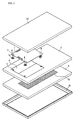
- Fig. 1 is an exploded perspective view of a display device according to a first embodiment of the present invention
- Fig. 2 is a perspective view of a board supporting structure according to the first embodiment of the present invention.
- Fig. 3 is an exploded perspective view of the board supporting structure according to the first embodiment of the present invention.
- Fig. 4 is a perspective view of a connection member used to fix a board to a main frame according to the first embodiment the present invention
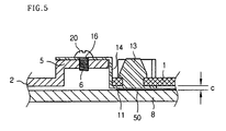
- Fig. 5 is a cross-sectional view taken along line I-I' of Fig. 1 ;
- Fig. 6 is an exploded perspective view of a display device according to a second embodiment of the present invention.
- Fig. 7 is a cross-sectional view taken along line II-II' of Fig. 6 ;
- Fig. 8 is a cross-sectional view illustrating a board supporting structure of a display device according to a third embodiment of the present invention.
- the display device includes a front cabinet 30 and a back cover 40 respectively protecting front and rear sides of the display device, a display module 8 providing an image actually, a main frame 2 fixed to a rear side of the display module 8, supporting a display module 8 and reinforcing the strength, and a board 1 installed at the main frame 2.
- the board 1 is fixed to the main frame 2 by a connection member 10, and a place where the board 1 is placed is aligned with a receiving portion 4.
- a receiving portion 4 is formed in the main frame 2.
- the receiving portion 4 may be formed in a shape having a height equal to the entire height of the main frame 2 and a predetermined area corresponding to an area of the board 1, or the receiving portion 4 may be recessed at a certain height in the main frame 2.
- the receiving portion 4 may be a predetermined hollow portion formed by cutting off a certain portion of the main frame 2 and thus allowing direct observation of the inside.
- the forming of the receiving portion 4 as the recessed portion or the hollow portion may advantageously prevent an increase in thickness of a display device occurring due to the installation of a board.
- the hollow receiving portion allows installation of a frame-side connection-member fixing portion 5 without an increase in thickness due to the thickness of the main frame 2 itself.
- the receiving portion will be illustrated as a hollow one.
- connection member 10 two portions are connected to the frame-side connection-member fixing portion 5 formed at the main frame 2 and a board-side connection-member fixing portion 3, respectively.
- various methods such as screw or catching may be used for the connection.
- an insulation material 50 is further formed on a rear surface of the display module 8 that is aligned with the receiving portion 4.
- the insulation material 50 prevents electrical discharge between the board 1 and the display module 8 and thus allows stable operation of the board 1. When a distance between the board 1 and the display module 8 is long, the insulation material 50 may not be needed. However, mounting the insulation material 50 is more desirable in order to reduce the thickness of the display device.
- connection member 10 is coupled to the board 1.
- the connection member 10 coupled to the board 1 is aligned with the frame-side connection-member fixing portion 5.
- a coupling member 20 such as a screw is inserted into the connection member 10 and the frame-side connection-member fixing portion 5, thereby entirely fixing the board 1 to the main frame 2.
- the main frame 2 may be a separate component that is fixed to the display module 8 in manufacturing the display device, or may be any component that is manufactured together with the display module 8 and reinforces the strength of the display module 8.
- the assembly is installed at a space between the front cabinet 30 and the back cover 40, thereby completing the manufacturing of the display device.
- the board supporting structure includes a board 1, a main frame 2 to which the board is fixed, and a connection member 10 fixing the board 1 to the main frame 2.
- a receiving portion 4 slightly wider than the main frame 2 is provided at one side of the main frame 2, and the board 1 is placed on and fixed to the receiving portion 4.
- At least one connection member 10 for fixing the board to the main frame 2 is coupled to an outer circumferential portion of the board 1.
- connection member 10 is coupled to the frame-side connection-member fixing portion 5 provided at the receiving portion 4 of the main frame 2 by a coupling member 20 such as a screw. In such a manner, the board 1 is fixed to the main frame 2.
- the main frame 2 is cut out to provide a receiving portion 4 on which the board 1 can be placed.
- the board 1 is fixed to the main frame 2 at a height equal to the main frame 2. Accordingly, an interval between the board and the main frame, which necessarily occurred when a board was installed at a main frame in the conventional art, is no longer generated.
- fixing the board 1 to the main frame 2 is achieved by coupling at least one connection member 10 to an outer circumferential portion of the board 1 and by fixing the connection member 10 to the main frame 2 with a connection member 20.
- board-side connection-member fixing portions 3 each having a pair of parallel slots, are formed at four corners of the board 1.
- a portion of the connection member 10 is penetratingly coupled to the board-side connection member fixing portion 3.
- connection members are coupled to the board at four corners of the board to face one another.
- positions of the connection-member fixing portions to which the connection members are coupled, and the number of connection members for fixing the board to the main frame may be modified in various manners.
- connection member 10 coupled to the board-side connection-member fixing part 3 includes a board support surface 11 placed to come in contact with a lower surface of the board 1 and supporting the board 1, a board coupling portion 12 protruding upward from one side of the support surface 11 and inserted to the board-side connection-member fixing portion 3, a vertical portion 14 extendingly upwardly from an outer corner of the support surface 11, and a frame coupling portion 15 extending from the vertical portion 14 outwardly of the support surface 11 and fixed to one side of the main frame 2.
- the board support surface 11 is formed to come in contact with a lower surface of the board 1 when the connection member 10 is coupled to the board 1.
- the board support surface 11 supports the board 1 when the board 1 is fixed to the main frame 2.
- the board coupling portion 12 protrudes upward from a corner of the support surface 11.
- a pair of board coupling portions 12 are formed side by side on the board support surface 11, corresponding to the slots of the board-side connection-member fixing portion 3 formed in the board 1.
- the board coupling portion 12 is formed as a protrusion having a sectional surface corresponding to the slot of the board-side connection-member fixing portion 3 and thusly can be inserted in the board-side connection-member fixing portion 3 of the board 1.
- the protrusion is formed at a height greater than a thickness of the board 1.
- a projection 13 having a wider width than that of the protrusion 12 is formed at an end portion of the board coupling portion 12. Accordingly, the entire board coupling portion 12 is formed as an arrow ( ⁇ ) shape facing upward.
- the board coupling portion 12 has a very thin section and thus can be moved when receiving an external force or twisted by hands.
- a coupling process between the board coupling portion 12 and the board-side connection-member fixing portion 3, performed by such a shape of the board coupling portion 12, will now be described.
- the board coupling portion 12 is penetratingly inserted in the board-side connection-member fixing portion 3. Then, the projection 13 placed at an upper side of the board coupling portion 12 protrudes to an upper surface of the board. Thereafter, the projection 13 is bended in a direction perpendicular to a slot direction of the board-side connection-member fixing portion 3. In such a state, the projection 13 may be fixed to the board 1 by using a certain method, e.g., welding or bonding.
- the vertical portion 14 extends upward from an outer corner of the connection member 10.
- the place where the vertical portion 14 is formed may come in contact with or be adjacent to a side surface of the board 1 when the board support surface 11 comes in contact with a lower side of the board 1.
- the length of the vertical portion 14 extending upward is greater than the thickness of the board, so that the board may be placed at a sufficiently low place, thereby preventing the thickness of the board 1 from affecting the thickness of the display device.
- the frame coupling portion 15 is formed at an end of the vertical portion outwardly of the board 1.
- a screw hole 16 is formed at the center of the frame coupling portion 15.
- the coupling member 20 such as a screw penetrates the screw hole 16 and is coupled to the frame-side connection-member fixing portion 5 formed at the main frame 2, thereby connecting the connection member 10 to the main frame 2.
- the frame-side connection-member fixing portion 5 protrudes inwardly of the receiving portion 4 from an edge of the receiving portion 4.
- the frame-side connection-member fixing portion 5 is formed as a protrusion protruding upward from a plane where the receiving portion of the main frame 2 is formed, and works as a plane on which a lower side of the frame coupling portion 15 of the connection member 10 may be placed.
- the frame-side connection-member fixing portion 5 has at its upper surface, a screw receiving groove 6 through which the coupling member 20, such as a screw, having penetrated the frame coupling portion 15 of the connection member 10, can be coupled thereto.
- Fig. 5 The form that the board 1 is coupled to the main frame 2 by the aforementioned connection member 10 is illustrated in Fig. 5 , the cross-sectional view taken along line I-I' of Fig. 2 in detail.
- the board that is coupled to the main frame 2 by the board supporting structure is placed at a height equal to the main frame 2. It can be easily predicted that the board can be placed at a place lower than the main frame 2 when an interval between the main frame 2 and a display module 8 is sufficiently long.
- a predetermined interval (C) may be formed between the board 1 and the module 8 placed under the main frame 2.
- the interval is the minimum distance to prevent electric discharge occurring between the board 1 and the display module 8 due to the approach of an end of an electric discharged portion protruding downward from the board 1 to the module 8, and the sufficient interval therebetween is approximately 5-6mm.
- an insulation material 50 may be additionally provided on a surface of the display module 8 facing the board 1. When the insulation material 50 is further formed, the reliability of the electric insulation is improved and the possibility of the electric discharge is reduced. For this reason, the interval between the board 1 and the display module 8 can be even more reduced advantageously.
- the vertical portion 14 of the connection member is formed at a height equal to a height from a lower surface of the board 1 up to an upper surface of the substantial board thickness including electric parts mounted on the board. Accordingly, one side of the vertical portion 14 is fixed to the main frame 2, and the other side thereof is coupled to a lower side of the board 1, thereby supporting the board 1 with respect to the main frame 2.
- the use of the board supporting structure may allow a space economy to an extent greater than a thickness of the main frame itself and thus makes the display device thinner totally as much.
- connection member is formed in a shape bent at least one portion in a vertical direction, the connection member can elastically move vertically even during or after the coupling of the connection member. Therefore, the fixation of the board can be facilitated, and the fixation position of the board can be maintained against an external impact even after the board is fixed to the main frame. Also, the reliability of the performance of the board can be improved.
- a thin display device may be constructed.
- the board is fixed to the main frame using a special connection member, direct damage or scratch to the board which may occur during fixation of the board with a screw can be prevented.
- the second embodiment of the present invention is similar to the first embodiment, except for a connection member and structures of a board and a main frame at their portions where the connection member is coupled. Therefore, the connection member and the portions related thereto are described in detail, portions without specific description will cite the description of the first embodiment, and detailed description thereof will be omitted.
- connection member 60 is formed in a single plane shape, and both ends of the connection member 60 are connected to a board 1 and a main frame 2 by a connection screw, respectively.
- connection member 60 is formed straight to connect the main frame 2 with the board 1, and the board 1 and the main frame 2 are placed at the same actual height. Accordingly, the entire thickness of the display device can be reduced.
- connection member 60 no protruding portion is provided at a portion of the main frame 8 where the connection member 60 is connected. Accordingly, an installation height of the connection member 60 is not increased so that the entire thickness of the display device can be reduced. Of course, the possibility of electric discharge due to the small interval between the board 1 and the display module 8 may exist, but such electric discharge can be prevented by an insulation material 50.
- the board 1 and/or the main frame 8 coupled to the connection member 60 may be provided with a certain structure.
- the certain structure may have a similar shape to the board coupling portion 12 provided to the connection member to be caught and stopped and fixed thereby.
- connection member 60 comes in contact with upper surfaces of the board 1 and the main frame 8 in the drawing, it can be easily predicted that the connection member 60 is not limited thereto but comes in contact with lower surfaces of the board 1 and the main frame 8 at a certain position.
- connection member 60 is formed straight in the drawing, it can be easily predicted that the connection member 60 may include a predetermined elastically-deformed portion to support the board 1 with a certain level of elastic force.
- the third embodiment of the present invention is similar to the second embodiment, except for a structure of a main frame at its portion to which a connection member is coupled. Therefore, only the portion related to the main frame to which the connection member is mounted will be described in detail, portions without specific description will cite the description of the aforementioned embodiment, and detailed description thereof will be omitted.
- a frame-side connection-member fixing portion 5 is provided to the main frame 2 like the first embodiment. For this reason, an interval between the board 1 and the display module 8 becomes long, and therefore, an insulation material 50 may not be needed.
- forming the insulation material 50 as in other embodiments may more efficiently prevent electric discharge between the board 1 and the display module 8.
Landscapes
- Engineering & Computer Science (AREA)
- Microelectronics & Electronic Packaging (AREA)
- Devices For Indicating Variable Information By Combining Individual Elements (AREA)
Applications Claiming Priority (1)
| Application Number | Priority Date | Filing Date | Title |
|---|---|---|---|
| KR1020050104433A KR100727122B1 (ko) | 2005-11-02 | 2005-11-02 | Pcb 고정 구조 |
Publications (3)
| Publication Number | Publication Date |
|---|---|
| EP1784067A2 EP1784067A2 (en) | 2007-05-09 |
| EP1784067A3 EP1784067A3 (en) | 2009-08-19 |
| EP1784067B1 true EP1784067B1 (en) | 2011-07-06 |
Family
ID=37807751
Family Applications (1)
| Application Number | Title | Priority Date | Filing Date |
|---|---|---|---|
| EP06254716A Not-in-force EP1784067B1 (en) | 2005-11-02 | 2006-09-11 | Display device and board supporting structure |
Country Status (4)
| Country | Link |
|---|---|
| US (1) | US7839658B2 (ko) |
| EP (1) | EP1784067B1 (ko) |
| KR (1) | KR100727122B1 (ko) |
| CN (1) | CN1959851B (ko) |
Families Citing this family (14)
| Publication number | Priority date | Publication date | Assignee | Title |
|---|---|---|---|---|
| KR20100136804A (ko) * | 2009-06-19 | 2010-12-29 | 삼성전자주식회사 | 보드연결 브라켓 및 그를 구비한 전자기기 |
| EP2367411A3 (en) * | 2010-03-17 | 2015-03-18 | Kabushiki Kaisha Toshiba | Display apparatus and electronic apparatus |
| US8665160B2 (en) | 2011-01-31 | 2014-03-04 | Apple Inc. | Antenna, shielding and grounding |
| US8570736B2 (en) | 2011-01-31 | 2013-10-29 | Apple Inc. | Component assembly |
| US8587939B2 (en) * | 2011-01-31 | 2013-11-19 | Apple Inc. | Handheld portable device |
| US8911280B2 (en) | 2011-01-31 | 2014-12-16 | Apple Inc. | Apparatus for shaping exterior surface of a metal alloy casing |
| US8611100B2 (en) * | 2011-11-18 | 2013-12-17 | Shenzhen China Star Optoelectronics Technology Co., Ltd. | Display device back panel with adjustable PCB mounting seat |
| TW201345359A (zh) * | 2012-04-24 | 2013-11-01 | Wistron Corp | 電子裝置 |
| KR102415119B1 (ko) * | 2015-08-21 | 2022-06-30 | 삼성에스디아이 주식회사 | 회로기판을 구비한 장치 |
| JP2017073524A (ja) * | 2015-10-09 | 2017-04-13 | 株式会社東芝 | 筐体の基板取付構造及び電子機器 |
| KR102411371B1 (ko) * | 2015-12-10 | 2022-06-22 | 삼성전자주식회사 | 기판 고정 장치 및 그것이 적용된 전자 장치 |
| CN106686937A (zh) * | 2017-03-14 | 2017-05-17 | 深圳市华上科技有限公司 | 采用连接件进行固定的用电设备 |
| KR101994226B1 (ko) | 2017-12-20 | 2019-07-01 | 린나이코리아 주식회사 | Pcb고정용 브라켓을 구비한 조리기기 |
| KR20230100900A (ko) * | 2021-12-29 | 2023-07-06 | 삼성전자주식회사 | 디스플레이 장치 |
Family Cites Families (24)
| Publication number | Priority date | Publication date | Assignee | Title |
|---|---|---|---|---|
| JP2933845B2 (ja) * | 1995-02-17 | 1999-08-16 | 三菱電機株式会社 | 印刷回路基板取付装置 |
| US5973926A (en) * | 1996-02-29 | 1999-10-26 | Palo Alto Design Group, Inc. | Method and apparatus for attaching circuit board to chassis and forming solid ground connection using a single screw |
| TW417944U (en) | 1999-03-25 | 2001-01-01 | Hon Hai Prec Ind Co Ltd | Buckling device of computer base plate |
| JP2001345586A (ja) | 2000-06-02 | 2001-12-14 | Pioneer Electronic Corp | プラズマディスプレイ装置 |
| KR100519470B1 (ko) * | 2001-06-22 | 2005-10-07 | 주식회사 포스코 | 연소공기 흐름 조절용 유동식 선회기가 설치된 루프버너 |
| US6842333B2 (en) * | 2001-09-13 | 2005-01-11 | Lg Electronics, Inc. | Portable electronic device having LCD and touch screen |
| JP2004022695A (ja) | 2002-06-14 | 2004-01-22 | Pioneer Electronic Corp | シートおよびこのシートを用いた電子機器 |
| KR100863998B1 (ko) | 2002-06-19 | 2008-10-16 | 삼성전자주식회사 | 액정표시모듈 및 이를 이용한 액정표시장치 |
| US7102895B1 (en) * | 2002-07-01 | 2006-09-05 | Alcatel | Bracket assembly used to connect a plug-in card to a backplane |
| KR100465796B1 (ko) | 2002-07-16 | 2005-01-13 | 삼성전자주식회사 | 디스플레이장치 |
| CN1309248C (zh) * | 2002-08-02 | 2007-04-04 | Nec液晶技术株式会社 | 显示器和显示板的支撑框架及其制造方法 |
| KR200319026Y1 (ko) * | 2003-02-28 | 2003-07-04 | 주식회사 대우일렉트로닉스 | 데크 어셈블리의 고정 브라켓 |
| KR100529111B1 (ko) | 2003-09-08 | 2005-11-15 | 삼성에스디아이 주식회사 | 플라즈마 디스플레이 모듈 포장설비 |
| KR100625971B1 (ko) | 2003-10-10 | 2006-09-20 | 삼성에스디아이 주식회사 | 회로기판의 결합구조 및 접지구조가 개선된 플라즈마디스플레이 장치 |
| CN100397170C (zh) * | 2003-10-16 | 2008-06-25 | 明基电通股份有限公司 | 平面显示器及其面板模块 |
| US20050088092A1 (en) | 2003-10-17 | 2005-04-28 | Myoung-Kon Kim | Plasma display apparatus |
| CN2671057Y (zh) * | 2003-12-09 | 2005-01-12 | 志合电脑股份有限公司 | 随附平面显示面板的框架组成结构 |
| US6955554B2 (en) | 2004-01-27 | 2005-10-18 | Hon Hai Precision Ind. Co., Ltd. | Electrical connector assembly having board hold down |
| US20060109616A1 (en) * | 2004-11-19 | 2006-05-25 | Au Optronics Corporation | Back support panel for flat panel display and method of producing same |
| KR100751321B1 (ko) * | 2004-12-01 | 2007-08-22 | 삼성에스디아이 주식회사 | 샤시 베이스 조립체와, 이를 채용한 플라즈마 표시장치조립체 |
| KR100684721B1 (ko) * | 2005-01-12 | 2007-02-20 | 삼성에스디아이 주식회사 | 플라즈마 디스플레이 장치 |
| US7114974B2 (en) * | 2005-01-19 | 2006-10-03 | Hon Hai Precision Ind. Co., Ltd. | Electrical connector assembly having board hold down |
| KR100759550B1 (ko) * | 2005-01-20 | 2007-09-18 | 삼성에스디아이 주식회사 | 디스플레이 모듈 |
| KR20060126317A (ko) * | 2005-06-04 | 2006-12-07 | 삼성에스디아이 주식회사 | 플라즈마 표시 장치 |
-
2005
- 2005-11-02 KR KR1020050104433A patent/KR100727122B1/ko active IP Right Grant
-
2006
- 2006-07-11 US US11/483,551 patent/US7839658B2/en active Active
- 2006-07-28 CN CN2006101086645A patent/CN1959851B/zh not_active Expired - Fee Related
- 2006-09-11 EP EP06254716A patent/EP1784067B1/en not_active Not-in-force
Also Published As
| Publication number | Publication date |
|---|---|
| EP1784067A3 (en) | 2009-08-19 |
| US20070097023A1 (en) | 2007-05-03 |
| US7839658B2 (en) | 2010-11-23 |
| KR100727122B1 (ko) | 2007-06-12 |
| KR20070047565A (ko) | 2007-05-07 |
| CN1959851A (zh) | 2007-05-09 |
| CN1959851B (zh) | 2010-06-23 |
| EP1784067A2 (en) | 2007-05-09 |
Similar Documents
| Publication | Publication Date | Title |
|---|---|---|
| EP1784067B1 (en) | Display device and board supporting structure | |
| US7477528B2 (en) | Frame bracket for printed board assembly and plasma display device having the same | |
| US8897018B2 (en) | Display device and television receiver | |
| EP2043415B1 (en) | Image displaying apparatus | |
| US8446543B2 (en) | Chassis assembly for display apparatus | |
| US6905103B2 (en) | Display apparatus | |
| WO2014034440A1 (ja) | 取付部材、表示装置、及びテレビジョン受信機 | |
| JPH1084193A (ja) | 電子製品のサブ回路基板固定装置 | |
| US7791868B2 (en) | Display device | |
| CN101957645A (zh) | 电脑机箱 | |
| KR100480822B1 (ko) | 액정표시장치 모듈 | |
| US7999883B2 (en) | Display | |
| US20070076384A1 (en) | Chassis boss assembly and display apparatus including the same | |
| KR100319204B1 (ko) | 엘시디모듈및이를이용한액정표시장치 | |
| US20080036937A1 (en) | Liquid crystal display device and method fabricating the same | |
| KR20090023124A (ko) | 플라즈마 디스플레이 장치 | |
| JP2008129390A (ja) | 薄型表示装置 | |
| JP5251770B2 (ja) | スタンドホルダおよびスタンドホルダの取り付け構造 | |
| CN220711548U (zh) | 用于source-PCB的安装支架及电视机 | |
| EP2159627A1 (en) | Flat screen assembly | |
| KR100669429B1 (ko) | 플라즈마 디스플레이 장치 | |
| KR100462806B1 (ko) | 액정표시장치모듈 | |
| CN116312229A (zh) | 显示装置 | |
| EP2159626A1 (en) | Flat screen assembly | |
| JP2005276889A (ja) | 基板固定機能を備えたシャーシフレーム |
Legal Events
| Date | Code | Title | Description |
|---|---|---|---|
| PUAI | Public reference made under article 153(3) epc to a published international application that has entered the european phase |
Free format text: ORIGINAL CODE: 0009012 |
|
| 17P | Request for examination filed |
Effective date: 20060918 |
|
| AK | Designated contracting states |
Kind code of ref document: A2 Designated state(s): AT BE BG CH CY CZ DE DK EE ES FI FR GB GR HU IE IS IT LI LT LU LV MC NL PL PT RO SE SI SK TR |
|
| AX | Request for extension of the european patent |
Extension state: AL BA HR MK YU |
|
| PUAL | Search report despatched |
Free format text: ORIGINAL CODE: 0009013 |
|
| AK | Designated contracting states |
Kind code of ref document: A3 Designated state(s): AT BE BG CH CY CZ DE DK EE ES FI FR GB GR HU IE IS IT LI LT LU LV MC NL PL PT RO SE SI SK TR |
|
| AX | Request for extension of the european patent |
Extension state: AL BA HR MK RS |
|
| AKX | Designation fees paid |
Designated state(s): DE FR GB |
|
| GRAP | Despatch of communication of intention to grant a patent |
Free format text: ORIGINAL CODE: EPIDOSNIGR1 |
|
| GRAS | Grant fee paid |
Free format text: ORIGINAL CODE: EPIDOSNIGR3 |
|
| GRAA | (expected) grant |
Free format text: ORIGINAL CODE: 0009210 |
|
| AK | Designated contracting states |
Kind code of ref document: B1 Designated state(s): DE FR GB |
|
| REG | Reference to a national code |
Ref country code: GB Ref legal event code: FG4D |
|
| REG | Reference to a national code |
Ref country code: DE Ref legal event code: R096 Ref document number: 602006022898 Country of ref document: DE Effective date: 20110901 |
|
| PLBE | No opposition filed within time limit |
Free format text: ORIGINAL CODE: 0009261 |
|
| STAA | Information on the status of an ep patent application or granted ep patent |
Free format text: STATUS: NO OPPOSITION FILED WITHIN TIME LIMIT |
|
| 26N | No opposition filed |
Effective date: 20120411 |
|
| REG | Reference to a national code |
Ref country code: DE Ref legal event code: R097 Ref document number: 602006022898 Country of ref document: DE Effective date: 20120411 |
|
| PGFP | Annual fee paid to national office [announced via postgrant information from national office to epo] |
Ref country code: DE Payment date: 20130813 Year of fee payment: 8 |
|
| PGFP | Annual fee paid to national office [announced via postgrant information from national office to epo] |
Ref country code: FR Payment date: 20130813 Year of fee payment: 8 Ref country code: GB Payment date: 20130812 Year of fee payment: 8 |
|
| REG | Reference to a national code |
Ref country code: DE Ref legal event code: R119 Ref document number: 602006022898 Country of ref document: DE |
|
| GBPC | Gb: european patent ceased through non-payment of renewal fee |
Effective date: 20140911 |
|
| REG | Reference to a national code |
Ref country code: DE Ref legal event code: R119 Ref document number: 602006022898 Country of ref document: DE Effective date: 20150401 |
|
| REG | Reference to a national code |
Ref country code: FR Ref legal event code: ST Effective date: 20150529 |
|
| PG25 | Lapsed in a contracting state [announced via postgrant information from national office to epo] |
Ref country code: DE Free format text: LAPSE BECAUSE OF NON-PAYMENT OF DUE FEES Effective date: 20150401 Ref country code: GB Free format text: LAPSE BECAUSE OF NON-PAYMENT OF DUE FEES Effective date: 20140911 |
|
| PG25 | Lapsed in a contracting state [announced via postgrant information from national office to epo] |
Ref country code: FR Free format text: LAPSE BECAUSE OF NON-PAYMENT OF DUE FEES Effective date: 20140930 |