EP1770747A2 - Plasma display panel and method for driving same - Google Patents
Plasma display panel and method for driving same Download PDFInfo
- Publication number
- EP1770747A2 EP1770747A2 EP06121444A EP06121444A EP1770747A2 EP 1770747 A2 EP1770747 A2 EP 1770747A2 EP 06121444 A EP06121444 A EP 06121444A EP 06121444 A EP06121444 A EP 06121444A EP 1770747 A2 EP1770747 A2 EP 1770747A2
- Authority
- EP
- European Patent Office
- Prior art keywords
- electrodes
- display panel
- plasma display
- substrate
- voltage
- Prior art date
- Legal status (The legal status is an assumption and is not a legal conclusion. Google has not performed a legal analysis and makes no representation as to the accuracy of the status listed.)
- Granted
Links
Images






Classifications
-
- G—PHYSICS
- G09—EDUCATION; CRYPTOGRAPHY; DISPLAY; ADVERTISING; SEALS
- G09G—ARRANGEMENTS OR CIRCUITS FOR CONTROL OF INDICATING DEVICES USING STATIC MEANS TO PRESENT VARIABLE INFORMATION
- G09G3/00—Control arrangements or circuits, of interest only in connection with visual indicators other than cathode-ray tubes
- G09G3/20—Control arrangements or circuits, of interest only in connection with visual indicators other than cathode-ray tubes for presentation of an assembly of a number of characters, e.g. a page, by composing the assembly by combination of individual elements arranged in a matrix no fixed position being assigned to or needed to be assigned to the individual characters or partial characters
- G09G3/22—Control arrangements or circuits, of interest only in connection with visual indicators other than cathode-ray tubes for presentation of an assembly of a number of characters, e.g. a page, by composing the assembly by combination of individual elements arranged in a matrix no fixed position being assigned to or needed to be assigned to the individual characters or partial characters using controlled light sources
- G09G3/28—Control arrangements or circuits, of interest only in connection with visual indicators other than cathode-ray tubes for presentation of an assembly of a number of characters, e.g. a page, by composing the assembly by combination of individual elements arranged in a matrix no fixed position being assigned to or needed to be assigned to the individual characters or partial characters using controlled light sources using luminous gas-discharge panels, e.g. plasma panels
- G09G3/288—Control arrangements or circuits, of interest only in connection with visual indicators other than cathode-ray tubes for presentation of an assembly of a number of characters, e.g. a page, by composing the assembly by combination of individual elements arranged in a matrix no fixed position being assigned to or needed to be assigned to the individual characters or partial characters using controlled light sources using luminous gas-discharge panels, e.g. plasma panels using AC panels
- G09G3/291—Control arrangements or circuits, of interest only in connection with visual indicators other than cathode-ray tubes for presentation of an assembly of a number of characters, e.g. a page, by composing the assembly by combination of individual elements arranged in a matrix no fixed position being assigned to or needed to be assigned to the individual characters or partial characters using controlled light sources using luminous gas-discharge panels, e.g. plasma panels using AC panels controlling the gas discharge to control a cell condition, e.g. by means of specific pulse shapes
- G09G3/292—Control arrangements or circuits, of interest only in connection with visual indicators other than cathode-ray tubes for presentation of an assembly of a number of characters, e.g. a page, by composing the assembly by combination of individual elements arranged in a matrix no fixed position being assigned to or needed to be assigned to the individual characters or partial characters using controlled light sources using luminous gas-discharge panels, e.g. plasma panels using AC panels controlling the gas discharge to control a cell condition, e.g. by means of specific pulse shapes for reset discharge, priming discharge or erase discharge occurring in a phase other than addressing
- G09G3/2927—Details of initialising
-
- G—PHYSICS
- G09—EDUCATION; CRYPTOGRAPHY; DISPLAY; ADVERTISING; SEALS
- G09G—ARRANGEMENTS OR CIRCUITS FOR CONTROL OF INDICATING DEVICES USING STATIC MEANS TO PRESENT VARIABLE INFORMATION
- G09G3/00—Control arrangements or circuits, of interest only in connection with visual indicators other than cathode-ray tubes
- G09G3/20—Control arrangements or circuits, of interest only in connection with visual indicators other than cathode-ray tubes for presentation of an assembly of a number of characters, e.g. a page, by composing the assembly by combination of individual elements arranged in a matrix no fixed position being assigned to or needed to be assigned to the individual characters or partial characters
- G09G3/22—Control arrangements or circuits, of interest only in connection with visual indicators other than cathode-ray tubes for presentation of an assembly of a number of characters, e.g. a page, by composing the assembly by combination of individual elements arranged in a matrix no fixed position being assigned to or needed to be assigned to the individual characters or partial characters using controlled light sources
- G09G3/28—Control arrangements or circuits, of interest only in connection with visual indicators other than cathode-ray tubes for presentation of an assembly of a number of characters, e.g. a page, by composing the assembly by combination of individual elements arranged in a matrix no fixed position being assigned to or needed to be assigned to the individual characters or partial characters using controlled light sources using luminous gas-discharge panels, e.g. plasma panels
- G09G3/288—Control arrangements or circuits, of interest only in connection with visual indicators other than cathode-ray tubes for presentation of an assembly of a number of characters, e.g. a page, by composing the assembly by combination of individual elements arranged in a matrix no fixed position being assigned to or needed to be assigned to the individual characters or partial characters using controlled light sources using luminous gas-discharge panels, e.g. plasma panels using AC panels
- G09G3/296—Driving circuits for producing the waveforms applied to the driving electrodes
-
- H—ELECTRICITY
- H01—ELECTRIC ELEMENTS
- H01J—ELECTRIC DISCHARGE TUBES OR DISCHARGE LAMPS
- H01J11/00—Gas-filled discharge tubes with alternating current induction of the discharge, e.g. alternating current plasma display panels [AC-PDP]; Gas-filled discharge tubes without any main electrode inside the vessel; Gas-filled discharge tubes with at least one main electrode outside the vessel
- H01J11/10—AC-PDPs with at least one main electrode being out of contact with the plasma
- H01J11/12—AC-PDPs with at least one main electrode being out of contact with the plasma with main electrodes provided on both sides of the discharge space
-
- H—ELECTRICITY
- H01—ELECTRIC ELEMENTS
- H01J—ELECTRIC DISCHARGE TUBES OR DISCHARGE LAMPS
- H01J11/00—Gas-filled discharge tubes with alternating current induction of the discharge, e.g. alternating current plasma display panels [AC-PDP]; Gas-filled discharge tubes without any main electrode inside the vessel; Gas-filled discharge tubes with at least one main electrode outside the vessel
- H01J11/20—Constructional details
- H01J11/34—Vessels, containers or parts thereof, e.g. substrates
- H01J11/40—Layers for protecting or enhancing the electron emission, e.g. MgO layers
-
- G—PHYSICS
- G09—EDUCATION; CRYPTOGRAPHY; DISPLAY; ADVERTISING; SEALS
- G09G—ARRANGEMENTS OR CIRCUITS FOR CONTROL OF INDICATING DEVICES USING STATIC MEANS TO PRESENT VARIABLE INFORMATION
- G09G2310/00—Command of the display device
- G09G2310/06—Details of flat display driving waveforms
- G09G2310/066—Waveforms comprising a gently increasing or decreasing portion, e.g. ramp
-
- G—PHYSICS
- G09—EDUCATION; CRYPTOGRAPHY; DISPLAY; ADVERTISING; SEALS
- G09G—ARRANGEMENTS OR CIRCUITS FOR CONTROL OF INDICATING DEVICES USING STATIC MEANS TO PRESENT VARIABLE INFORMATION
- G09G2320/00—Control of display operating conditions
- G09G2320/04—Maintaining the quality of display appearance
- G09G2320/041—Temperature compensation
Definitions
- the present invention relates to a plasma display panel (PDP) and a method for driving the same.
- PDP plasma display panel
- a plasma display panel is a flat display device using a plasma phenomenon, which is also called a gas-discharge phenomenon since a discharge is generated in the panel when a potential is applied to two electrodes separated from each other under a gas atmosphere in a non-vacuum state.
- a gas discharge phenomenon is used to display an image.
- a PDP has a matrix structure where electrodes are provided on opposing substrates and arranged to cross and face each other, with a discharge gas between two substrates.
- DC direct current
- AC alternating current
- AC-PDPs have a basic structure in which electrodes are arranged to cross and face each other in a space between two substrates filled with a discharge gas. The space is partitioned with barrier ribs. One electrode is coated with a dielectric layer for forming wall charges thereon, and a phosphor layer is formed on the facing side of the other electrode.
- the barrier ribs and the dielectric layer are generally formed by printing methods, and the layers tend to be thick.
- such grown layers tend to have inferior qualities compared to those formed using a thin film fabrication process.
- the dielectric layer and the electrode under the dielectric layer may be damaged by sputtering of electrons and ions generated from the discharge and thus the life-span of the AC-PDP may be shortened.
- An exemplary embodiment of the present invention provides a plasma display panel (PDP) that can shorten response delay time by using extremely pure MgO to form a protective layer on the dielectric layer to prevent unstable discharge based on temperature, and a method for driving the same.
- PDP plasma display panel
- a plasma display panel which includes: a first substrate and a second substrate arranged substantially parallel to one another and spaced apart from one another; a plurality of address electrodes formed on the first substrate; a first dielectric layer formed on the first substrate and covering the address electrodes; a plurality of barrier ribs having a given height and forming a discharge space with the first dielectric layer; a phosphor layer formed in the discharge space; a plurality of sustain electrodes formed on the second substrate opposite the first substrate and arranged crossing the address electrodes; a second dielectric layer formed on the second substrate and covering the sustain electrodes; and a protective layer including MgO having a purity of at least 99.6% by weight and covering the second dielectric layer.
- a method for driving a plasma display panel includes first electrodes and second electrodes formed on a first substrate and parallel to each other, third electrodes formed on a second substrate and crossing the first electrodes and the second electrodes, a dielectric layer formed on the second substrate and covering the first and second electrodes, and a protective layer covering the dielectric layer and having a purity of at least 99.6% by weight of MgO.
- the method includes: determining the temperature of the plasma display panel; applying a voltage that gradually decreases from a first voltage to a second voltage to the first electrodes; and sustaining application of the second voltage to the first electrode in a first period of a reset period, wherein the first period is varied according to the temperature of the plasma display panel.
- the present invention provides a protective layer in a plasma display panel (PDP), and an example of a PDP having the protective layer is shown in Figure 1.
- the plasma display panel includes a first substrate 1 and a second substrate 11 the two substrates arranged generally parallel to and spaced apart from one another.
- a plurality of generally parallel address electrodes 3 are formed on the first substrate 1 along direction Y of Figure 1, and a dielectric layer 5 is formed on the surface of the first substrate 1 and over the address electrodes 3.
- Barrier ribs 7 are arranged on the dielectric layer 5 parallel to the address electrodes and may be formed in an open or closed shape. Red (R), green (G), and blue (B) phosphor layers 9 are positioned on the dielectric layer 5 and between adjacent barrier ribs 7.
- a plurality of parallel display electrodes 13 are formed in direction X in Figure 1 which is a direction generally perpendicular to the direction of the address electrodes.
- Each display electrode 13 comprises a pair of transparent electrodes 13a and a pair of bus electrodes where each transparent electrode 13a is further paired with a corresponding bus electrode 13b.
- a transparent dielectric layer 15 and a protective layer 17 are formed over the second substrate 11, and covering the display electrodes 13.
- One of the electrodes of the pair of electrodes of each display electrode 13 is a sustain electrode (X electrode), and the other is a scan electrode (Y electrode).
- a discharge cell is formed by each intersection of a particular address electrode 3 and a perpendicular display electrode 13, and is filled with a discharge gas.
- the protective layer 17 of the plasma display panel includes extremely pure MgO having a purity of at least 99.6% by weight, and more specifically a purity ranging from over 99.8% to 100% by weight.
- the extremely pure MgO may include an impurity selected from the group consisting of Ca, Al, Si, Fe, Zn, Na, Cr, Mn, and combinations thereof.
- the extremely pure MgO may be a polycrystalline MgO prepared according to a sintering method.
- the protective layer includes the extremely pure MgO prepared by a sintering method, it may have a quick response property but the discharge characteristic may be unstable depending on temperature.
- wall charges may be unstable at low and high temperatures, and low discharge may occur.
- another embodiment of the invention involves a method for operating a plasma display panel.
- FIG. 2 is a block view showing a structure of a plasma display panel 100 in accordance with an embodiment of the present invention.
- the plasma display panel 100 includes a plurality of address electrodes A1 to Am arranged in columns, and a plurality of sustain electrodes X1 to Xn and a plurality of scan electrodes Y1 to Yn arranged in rows with each sustain electrode paired with a scan electrode.
- the sustain electrodes X1 to Xn are disposed in opposite directions to the scan electrodes Y1 to Yn.
- the sustain electrodes X1 to Xn and the scan electrodes Y1 to Yn are respectively coupled to each other at one end of thereof.
- the plasma display panel 100 comprises a first substrate (not shown) where the address electrodes A1 to Am are arranged, and a second substrate (not shown) where the sustain electrodes X1 to Xn and the scan electrodes Y1 to Yn are arranged.
- the two substrates face one another with a discharge space between them such that the scan electrodes Y1 to Yn and the sustain electrodes X1 to Xn cross the address electrodes A1 to Am.
- Discharge cells are formed at the positions where the address electrodes A1 to Am cross an electrode pair comprising a sustain electrode X1 to Xn and a scan electrode Y1 to Yn.
- An address driver 300 receives an address driving control signal from a controller 200 and applies a display data signal for selecting a discharge cell to be displayed to a corresponding address electrode.
- a sustain electrode driver 400 receives a sustain electrode driving control signal from the controller 200 and applies a driving voltage to the sustain electrodes X1 to Xn.
- a scan electrode driver 500 receives a scan electrode driving control signal from the controller 200 and applies a driving voltage to the scan electrodes.
- a temperature detector 600 senses the temperature of the plasma display panel 100 and transmits temperature information to the controller 200. It is possible to directly sense the temperature of the plasma display panel 100 by setting up a thermosensor inside of the plasma display panel 100, or to indirectly sense the temperature of the plasma display panel 100 by setting up a thermosensor at the back of the plasma display panel 100. Since methods for sensing temperature of plasma display panels are known per se to those skilled in the art, a detailed description will not be provided here.
- the controller 200 receives external video signals and outputs an address driving control signal, a sustain electrode driving control signal, and a scan electrode driving control signal.
- the controller 200 divides one frame into a plurality of subfields, and each subfield comprises a reset period, an address period, and a sustain period when the subfield is expressed based on temporal driving change.
- the reset period is for initializing the status of each discharge cell so as to facilitate an addressing operation on the discharge cell
- the address period is for accumulating wall charges by applying an address voltage to the addressed cells which are to be turned on, and to select cells to be turned on and cells to be turned off in the plasma display panel.
- the sustain period is for performing discharge to actually display images in the addressed cells by applying a sustain pulse.
- the controller 200 receives temperature information for the plasma display panel 100 from the temperature detector 600, and it generates a scan electrode driving control signal for varying a Vset voltage applying time (T1) or a Vnf voltage applying time (T2) in the reset period depending on the temperature of the plasma display panel 100.
- the scan electrode driving control signal generated in the controller 200 is transmitted to the scan electrode driver 500.
- the scan electrode driver 500 drives the scan electrodes to vary the Vset voltage applying time (T1) or the Vnf voltage applying time (T2) in the reset period based on the scan electrode driving control signal.
- the controller 200 causes wall charges to be sufficiently accumulated by increasing the Vset voltage applying time (T1).
- the controller 200 causes wall charges to be sufficiently accumulated by increasing the Vnf voltage applying time (T2).
- a driving waveform to be applied to the scan electrodes Y1 to Yn, which will be simply referred to as Y, during the reset period for each subfield will now be described with reference to Figures 3 and 4.
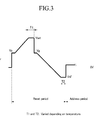
- Figure 3 shows a driving waveform of a PDP in accordance with an embodiment of the present invention.
- Figure 3 shows only a driving waveform applied to the scan electrodes Y in the reset period of each subfield, and driving waveforms applied to the address electrodes A1 to Am and the sustain electrodes X1 to Xn, which will be simply referred to as A and X, respectively, in the address period and the sustain period were omitted herein for the sake of convenience of description.
- a Vset voltage having a T1 period is applied to the scan electrodes Y.
- the Vset voltage is applied for the T1 period to sufficiently accumulate negative wall charges in the scan electrodes Y and positive wall charges in the sustain electrodes X and the address electrodes A.
- the T1 period is varied according to the temperature of the plasma display panel. In other words, when a protective layer including the extremely pure MgO is prepared using a sintering method, wall charges are not sufficiently accumulated below a given first temperature level which is a low temperature level, and above a given second temperature level which is a high temperature level. Therefore, the T1 period is increased to sufficiently accumulate the wall charges generated during the weak discharge in the electrodes.
- the first temperature level and the second temperature level used to increase the T1 period are determined to be the temperatures at which the wall charges are not accumulated sufficiently according to the state of the plasma display panel. Such temperature levels can be determined through experiments by those skilled in the art, and therefore, a detailed description will not be provided here.
- a voltage gradually decreasing from a Vg voltage to a Vnf voltage is applied to the scan electrodes Y in a falling period of the reset period.
- a reference voltage i.e., 0V
- a Ve voltage which is a positive voltage
- weak reset discharge occurs between the scan electrodes Y and the sustain electrodes X and between the scan electrodes Y and the address electrodes A while the voltage of the scan electrodes Y decreases, and thus the negative wall charges generated in the scan electrodes Y and the positive wall charges formed in the sustain electrodes X and the address electrodes A are eliminated.
- the Vnf voltage is applied to the scan electrodes Y, and sustained for a period T2 to sufficiently accumulate wall charges for addressing.
- the T2 period is varied depending on the temperature.
- the protective layer includes the extremely pure MgO prepared by a sintering method
- wall charges are not properly accumulated below a predetermined third temperature level, which is a low temperature, or above a predetermined fourth temperature level, which is a high temperature. Therefore, the T2 period is increased to properly accumulate wall charges in the electrodes during the weak discharge caused in a falling period of the reset period.
- the third temperature level and the fourth temperature level that are used to increase the T2 period are determined to be temperatures at which wall charges are not properly accumulated according to the status of the plasma display panel.
- the third temperature level and the fourth temperature level may be determined through experiments.
- the T2 period is controlled to be more than or equal to 40 ⁇ s to accumulate wall charges sufficiently.
- the T2 period may be controlled to be shorter than or equal to 60 ⁇ s.
- the method for determining the third temperature and the fourth temperature is known to those skilled in the art, and a detailed description will not be provided here.
- Figure 3 shows a waveform obtained by applying a gradually increasing voltage and a gradually decreasing voltage to the scan electrodes Y in the reset period, it is possible to perform a reset by applying a gradually decreasing waveform to the scan electrode Y.
- Figure 4 shows a driving waveform of the plasma display panel in accordance with another embodiment of the present invention.
- Vs voltage is a sustain discharge pulse voltage applied in the sustain period of a previous subfield.
- reset discharge occurs only in the discharge cells selected in the previous subfield to thereby generate wall charges sufficient for addressing.
- the reset discharge does not occur in the discharge cells not selected in the previous subfield, and the status of wall charges after the reset period of the previous subfield is sustained.
- U.S. Patent No. 6,294,875 to Kurata et al. discloses details thereof.
- the Vnf voltage applying time (T3) is also varied according to temperature, just as in the first embodiment. Since the method of varying the T3 period according to temperature is the same as that of the first embodiment, a detailed description will not be provided here.
- the T3 period may be controlled to be greater than or equal to 40 ⁇ s to sufficiently accumulate wall charges.
- the T3 period may also be controlled to be shorter than or equal to 70 ⁇ s.
- the low discharge problem can be resolved by varying the Vset voltage applying time or the Vnf voltage applying time according to the temperature of the plasma display panel in order to sufficiently accumulate the wall charges as shown in the embodiments of the present invention described above.
- Stripe-type sustain electrodes were formed of an indium tin oxide conductive material on an upper substrate formed of soda lime glass using a conventional sustain electrode forming method.
- a dielectric layer was then formed over the sustain electrodes and on the upper substrate by coating the entire surface of the upper substrate with a lead-based glass paste and baking the upper substrate.
- An upper panel was prepared by forming a protective layer of a MgO compound on the dielectric layer by using a sputtering method.
- the MgO compound was prepared through a sintering process, and had a purity of at least 99.6% by weight.
- the impurities of the MgO compound are revealed in Table 1 below.
- Example 1 The same process as in Example 1 was carried out, except that the waveforms of Figures 3 and 4 were applied to the plasma display panel prepared in accordance with Example 1.
- Example 1 The same process as in Example 1 was carried out, except that a MgO compound including the impurities shown in Table 1 was used.
- the purity of the MgO compound can be calculated from the contents of the impurities by subtracting the contents of the impurities from the MgO compound.
- Example 1 The same process as in Example 1 was carried out, except that a MgO compound including the impurities shown in Table 1 was used.
- the purity of the MgO compound can be calculated from the contents of the impurities by subtracting the contents of the impurities from the MgO compound.
- the contents of the MgO compound used in Example 1 and Comparative Examples 1 and 2 are shown in the following Table 1. Since the impurity contents of Example 2 were the same as in Example 1, they are not presented in Table 1.
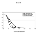
- Discharge delay times for the plasma display panels prepared in accordance with Examples 1 and 2 and Comparative Examples 1 and 2 were measured at a low temperature (-10°C), at room temperature (25°C), and at a high temperature (60° C), and the results are presented in Figures 5 to 8.
- the discharge delay times at each temperature are presented in Table 2.
- the y-axis indicates a relative discharge failure index.
- Table 2 Low temperature (nsec) Room temperature (nsec) High temperature (nsec) Comparative Example 1 517 421 378 Comparative Example 2 489 395 352
- Example 1 and 2 As shown in Table 2 and Figures 5 to 8, the discharge delay time is different according to temperature, and the discharge delay times of Example 1 and 2 were remarkably shorter than those of Comparative Examples 1 and 2.
- the present invention can stabilize discharge where a plasma display panel includes a protective layer including an extremely pure MgO prepared by a sintering method, by varying a Vset applying time or a Vnf voltage applying time according to the temperature of the plasma display panel in order to sufficiently accumulate wall charges in the reset period.
Landscapes
- Engineering & Computer Science (AREA)
- Physics & Mathematics (AREA)
- Plasma & Fusion (AREA)
- Power Engineering (AREA)
- Computer Hardware Design (AREA)
- General Physics & Mathematics (AREA)
- Theoretical Computer Science (AREA)
- Control Of Gas Discharge Display Tubes (AREA)
- Gas-Filled Discharge Tubes (AREA)
- Control Of Indicators Other Than Cathode Ray Tubes (AREA)
Abstract
Description
- The present invention relates to a plasma display panel (PDP) and a method for driving the same.
- A plasma display panel (PDP) is a flat display device using a plasma phenomenon, which is also called a gas-discharge phenomenon since a discharge is generated in the panel when a potential is applied to two electrodes separated from each other under a gas atmosphere in a non-vacuum state. Such a gas discharge phenomenon is used to display an image. Basically, a PDP has a matrix structure where electrodes are provided on opposing substrates and arranged to cross and face each other, with a discharge gas between two substrates.
- There are two general types of plasma display panels: a direct current (DC) type and an alternating current (AC) type. Among them, the AC-PDPs are most widely used.
- AC-PDPs have a basic structure in which electrodes are arranged to cross and face each other in a space between two substrates filled with a discharge gas. The space is partitioned with barrier ribs. One electrode is coated with a dielectric layer for forming wall charges thereon, and a phosphor layer is formed on the facing side of the other electrode.
- For cost reasons, the barrier ribs and the dielectric layer are generally formed by printing methods, and the layers tend to be thick. However, such grown layers tend to have inferior qualities compared to those formed using a thin film fabrication process.
- Therefore, there is a problem in that the dielectric layer and the electrode under the dielectric layer may be damaged by sputtering of electrons and ions generated from the discharge and thus the life-span of the AC-PDP may be shortened.
- An exemplary embodiment of the present invention provides a plasma display panel (PDP) that can shorten response delay time by using extremely pure MgO to form a protective layer on the dielectric layer to prevent unstable discharge based on temperature, and a method for driving the same.
- According to an embodiment of the present invention, a plasma display panel is provided which includes: a first substrate and a second substrate arranged substantially parallel to one another and spaced apart from one another; a plurality of address electrodes formed on the first substrate; a first dielectric layer formed on the first substrate and covering the address electrodes; a plurality of barrier ribs having a given height and forming a discharge space with the first dielectric layer; a phosphor layer formed in the discharge space; a plurality of sustain electrodes formed on the second substrate opposite the first substrate and arranged crossing the address electrodes; a second dielectric layer formed on the second substrate and covering the sustain electrodes; and a protective layer including MgO having a purity of at least 99.6% by weight and covering the second dielectric layer.
- According to another embodiment of the present invention, a method for driving a plasma display panel is provided. The plasma display panel includes first electrodes and second electrodes formed on a first substrate and parallel to each other, third electrodes formed on a second substrate and crossing the first electrodes and the second electrodes, a dielectric layer formed on the second substrate and covering the first and second electrodes, and a protective layer covering the dielectric layer and having a purity of at least 99.6% by weight of MgO. The method includes: determining the temperature of the plasma display panel; applying a voltage that gradually decreases from a first voltage to a second voltage to the first electrodes; and sustaining application of the second voltage to the first electrode in a first period of a reset period, wherein the first period is varied according to the temperature of the plasma display panel.
- In order that the invention may be more fully understood embodiments thereof will now be described by way of example with reference to the accompanying drawings wherein:
- Figure 1 is a perspective view showing the structure of a plasma display panel (PDP) in accordance with an embodiment of the present invention;
- Figure 2 is a block view illustrating the structure of a plasma display panel in accordance with an embodiment of the present invention;
- Figure 3 shows a driving waveform of a plasma display panel according to an embodiment of the present invention;
- Figure 4 shows a driving waveform of a plasma display panel according to another embodiment of the present invention;
- Figure 5 is a graph showing the discharge delay time of a plasma display panel prepared according to Example 1;
- Figure 6 is a graph showing the discharge delay time of a plasma display panel prepared according to Example 2;
- Figure 7 is a graph showing the discharge delay time of a plasma display panel prepared according to Comparative Example 1; and
- Figure 8 is a graph showing the discharge delay time of a plasma display panel prepared according to Comparative Example 2.
- The present invention provides a protective layer in a plasma display panel (PDP), and an example of a PDP having the protective layer is shown in Figure 1. As shown in Figure 1, the plasma display panel includes a first substrate 1 and a
second substrate 11 the two substrates arranged generally parallel to and spaced apart from one another. A plurality of generallyparallel address electrodes 3 are formed on the first substrate 1 along direction Y of Figure 1, and adielectric layer 5 is formed on the surface of the first substrate 1 and over theaddress electrodes 3.Barrier ribs 7 are arranged on thedielectric layer 5 parallel to the address electrodes and may be formed in an open or closed shape. Red (R), green (G), and blue (B) phosphor layers 9 are positioned on thedielectric layer 5 and betweenadjacent barrier ribs 7. - On the surface of the
second substrate 11 facing the first substrate 1, a plurality ofparallel display electrodes 13 are formed in direction X in Figure 1 which is a direction generally perpendicular to the direction of the address electrodes. Eachdisplay electrode 13 comprises a pair oftransparent electrodes 13a and a pair of bus electrodes where eachtransparent electrode 13a is further paired with acorresponding bus electrode 13b. A transparentdielectric layer 15 and aprotective layer 17 are formed over thesecond substrate 11, and covering thedisplay electrodes 13. One of the electrodes of the pair of electrodes of eachdisplay electrode 13 is a sustain electrode (X electrode), and the other is a scan electrode (Y electrode). A discharge cell is formed by each intersection of aparticular address electrode 3 and aperpendicular display electrode 13, and is filled with a discharge gas. - The
protective layer 17 of the plasma display panel includes extremely pure MgO having a purity of at least 99.6% by weight, and more specifically a purity ranging from over 99.8% to 100% by weight. The extremely pure MgO may include an impurity selected from the group consisting of Ca, Al, Si, Fe, Zn, Na, Cr, Mn, and combinations thereof. - The extremely pure MgO may be a polycrystalline MgO prepared according to a sintering method. When the protective layer includes the extremely pure MgO prepared by a sintering method, it may have a quick response property but the discharge characteristic may be unstable depending on temperature. In particular, when the protective layer includes the extremely pure MgO prepared by a sintering method, wall charges may be unstable at low and high temperatures, and low discharge may occur.
- When the temperature is low, charges are transferred slowly and thus the response rate of discharge becomes slow and it takes a somewhat long time to accumulate wall charges. Therefore, wall charges cannot be sufficiently accumulated using a reset period and the probability that address discharge is not completed within an address period is increased. This causes a problem of low discharge.
- In contrast, when the temperature is high, charges are transferred fast and the discharge response rate becomes quick. Therefore, over-accumulated charges may be self-eliminated in the reset period or may be transferred into adjacent discharge cells before they are addressed. Since the wall charges cannot be accumulated sufficiently, there may also be a low discharge problem in which address discharge does not occur properly.
- To avoid such problems in the operation of a plasma display panel that uses an extremely pure MgO protective layer that is prepared by a sintering method another embodiment of the invention involves a method for operating a plasma display panel.
- Figure 2 is a block view showing a structure of a
plasma display panel 100 in accordance with an embodiment of the present invention. Theplasma display panel 100 includes a plurality of address electrodes A1 to Am arranged in columns, and a plurality of sustain electrodes X1 to Xn and a plurality of scan electrodes Y1 to Yn arranged in rows with each sustain electrode paired with a scan electrode. The sustain electrodes X1 to Xn are disposed in opposite directions to the scan electrodes Y1 to Yn. The sustain electrodes X1 to Xn and the scan electrodes Y1 to Yn are respectively coupled to each other at one end of thereof. Theplasma display panel 100 comprises a first substrate (not shown) where the address electrodes A1 to Am are arranged, and a second substrate (not shown) where the sustain electrodes X1 to Xn and the scan electrodes Y1 to Yn are arranged. The two substrates face one another with a discharge space between them such that the scan electrodes Y1 to Yn and the sustain electrodes X1 to Xn cross the address electrodes A1 to Am. Discharge cells are formed at the positions where the address electrodes A1 to Am cross an electrode pair comprising a sustain electrode X1 to Xn and a scan electrode Y1 to Yn. It should be apparent to one of skill in the art that the structure of theplasma display panel 100 of Figure 2 is just one example of a plasma display panel, and the present invention can be applied to plasma display panels of other structures to which the following driving waveform can be applied. - An
address driver 300 receives an address driving control signal from acontroller 200 and applies a display data signal for selecting a discharge cell to be displayed to a corresponding address electrode. - A
sustain electrode driver 400 receives a sustain electrode driving control signal from thecontroller 200 and applies a driving voltage to the sustain electrodes X1 to Xn. - A
scan electrode driver 500 receives a scan electrode driving control signal from thecontroller 200 and applies a driving voltage to the scan electrodes. - A
temperature detector 600 senses the temperature of theplasma display panel 100 and transmits temperature information to thecontroller 200. It is possible to directly sense the temperature of theplasma display panel 100 by setting up a thermosensor inside of theplasma display panel 100, or to indirectly sense the temperature of theplasma display panel 100 by setting up a thermosensor at the back of theplasma display panel 100. Since methods for sensing temperature of plasma display panels are known per se to those skilled in the art, a detailed description will not be provided here. - The
controller 200 receives external video signals and outputs an address driving control signal, a sustain electrode driving control signal, and a scan electrode driving control signal. Thecontroller 200 divides one frame into a plurality of subfields, and each subfield comprises a reset period, an address period, and a sustain period when the subfield is expressed based on temporal driving change. The reset period is for initializing the status of each discharge cell so as to facilitate an addressing operation on the discharge cell, and the address period is for accumulating wall charges by applying an address voltage to the addressed cells which are to be turned on, and to select cells to be turned on and cells to be turned off in the plasma display panel. The sustain period is for performing discharge to actually display images in the addressed cells by applying a sustain pulse. - According to an embodiment of the present invention, the
controller 200 receives temperature information for theplasma display panel 100 from thetemperature detector 600, and it generates a scan electrode driving control signal for varying a Vset voltage applying time (T1) or a Vnf voltage applying time (T2) in the reset period depending on the temperature of theplasma display panel 100. The scan electrode driving control signal generated in thecontroller 200 is transmitted to thescan electrode driver 500. Thescan electrode driver 500 drives the scan electrodes to vary the Vset voltage applying time (T1) or the Vnf voltage applying time (T2) in the reset period based on the scan electrode driving control signal. When the temperature of theplasma display panel 100 is lower than a given temperature, thecontroller 200 causes wall charges to be sufficiently accumulated by increasing the Vset voltage applying time (T1). When the temperature of theplasma display panel 100 is higher than the given temperature, thecontroller 200 causes wall charges to be sufficiently accumulated by increasing the Vnf voltage applying time (T2). - A driving waveform to be applied to the scan electrodes Y1 to Yn, which will be simply referred to as Y, during the reset period for each subfield will now be described with reference to Figures 3 and 4.
- Figure 3 shows a driving waveform of a PDP in accordance with an embodiment of the present invention. Figure 3 shows only a driving waveform applied to the scan electrodes Y in the reset period of each subfield, and driving waveforms applied to the address electrodes A1 to Am and the sustain electrodes X1 to Xn, which will be simply referred to as A and X, respectively, in the address period and the sustain period were omitted herein for the sake of convenience of description.
- Referring to the waveform of Figure 3, voltage gradually increases from voltage Vp to voltage Vset, and such voltage is applied to the scan electrodes Y during an increasing period of the reset period. Then, a weak reset discharge occurs from the scan electrodes Y to the address electrodes A and the sustain electrodes X, individually, to thereby generate negative wall charges in the scan electrodes Y and positive wall charges in the address electrodes A and the sustain electrodes X. When the voltage of the electrodes is gradually changed as shown in Figure 3, weak discharge occurs in the discharge cells and wall charges are generated such that a summation of voltage applied from the outside and the wall voltage of the discharge cells is the same as the voltage status before discharge. This principle is disclosed in
U.S. Patent No. 5,745,086 by Weber . Since all discharge cells should be initialized in the reset period, the Vset voltage should be sufficiently high to cause discharge in all cells. - Also, a Vset voltage having a T1 period is applied to the scan electrodes Y. The Vset voltage is applied for the T1 period to sufficiently accumulate negative wall charges in the scan electrodes Y and positive wall charges in the sustain electrodes X and the address electrodes A. In the embodiment of the present invention, the T1 period is varied according to the temperature of the plasma display panel. In other words, when a protective layer including the extremely pure MgO is prepared using a sintering method, wall charges are not sufficiently accumulated below a given first temperature level which is a low temperature level, and above a given second temperature level which is a high temperature level. Therefore, the T1 period is increased to sufficiently accumulate the wall charges generated during the weak discharge in the electrodes. The first temperature level and the second temperature level used to increase the T1 period are determined to be the temperatures at which the wall charges are not accumulated sufficiently according to the state of the plasma display panel. Such temperature levels can be determined through experiments by those skilled in the art, and therefore, a detailed description will not be provided here.
- Then, a voltage gradually decreasing from a Vg voltage to a Vnf voltage is applied to the scan electrodes Y in a falling period of the reset period. Although not shown in Figure 3, a reference voltage, i.e., 0V, is applied to the address electrodes A, and a Ve voltage, which is a positive voltage, is applied to the sustain electrodes X. Then, weak reset discharge occurs between the scan electrodes Y and the sustain electrodes X and between the scan electrodes Y and the address electrodes A while the voltage of the scan electrodes Y decreases, and thus the negative wall charges generated in the scan electrodes Y and the positive wall charges formed in the sustain electrodes X and the address electrodes A are eliminated.
- Subsequently, the Vnf voltage is applied to the scan electrodes Y, and sustained for a period T2 to sufficiently accumulate wall charges for addressing. The T2 period is varied depending on the temperature. In other words, when the protective layer includes the extremely pure MgO prepared by a sintering method, wall charges are not properly accumulated below a predetermined third temperature level, which is a low temperature, or above a predetermined fourth temperature level, which is a high temperature. Therefore, the T2 period is increased to properly accumulate wall charges in the electrodes during the weak discharge caused in a falling period of the reset period. The third temperature level and the fourth temperature level that are used to increase the T2 period are determined to be temperatures at which wall charges are not properly accumulated according to the status of the plasma display panel. The third temperature level and the fourth temperature level may be determined through experiments. According to the embodiment of the present invention, the T2 period is controlled to be more than or equal to 40µs to accumulate wall charges sufficiently. The T2 period may be controlled to be shorter than or equal to 60µs. The method for determining the third temperature and the fourth temperature is known to those skilled in the art, and a detailed description will not be provided here.
- While Figure 3 shows a waveform obtained by applying a gradually increasing voltage and a gradually decreasing voltage to the scan electrodes Y in the reset period, it is possible to perform a reset by applying a gradually decreasing waveform to the scan electrode Y.
- Figure 4 shows a driving waveform of the plasma display panel in accordance with another embodiment of the present invention.
- As shown in Figure 4, voltage gradually decreases from a Vs voltage to a Vnf voltage, and such voltage is applied to the scan electrodes Y in the reset period of Example 2. Herein, the Vs voltage is a sustain discharge pulse voltage applied in the sustain period of a previous subfield. When only a gradually decreasing voltage is applied to the scan electrodes Y, reset discharge occurs only in the discharge cells selected in the previous subfield to thereby generate wall charges sufficient for addressing. The reset discharge does not occur in the discharge cells not selected in the previous subfield, and the status of wall charges after the reset period of the previous subfield is sustained.
U.S. Patent No. 6,294,875 to Kurata et al. discloses details thereof. The Vnf voltage applying time (T3) is also varied according to temperature, just as in the first embodiment. Since the method of varying the T3 period according to temperature is the same as that of the first embodiment, a detailed description will not be provided here. The T3 period may be controlled to be greater than or equal to 40µs to sufficiently accumulate wall charges. The T3 period may also be controlled to be shorter than or equal to 70µs. - As described above, when the protective layer includes the extremely pure MgO prepared by a sintering method, the low discharge problem can be resolved by varying the Vset voltage applying time or the Vnf voltage applying time according to the temperature of the plasma display panel in order to sufficiently accumulate the wall charges as shown in the embodiments of the present invention described above.
- The following examples illustrate the present invention in more detail. However, it is understood that the present invention is not limited by these examples.
- Stripe-type sustain electrodes were formed of an indium tin oxide conductive material on an upper substrate formed of soda lime glass using a conventional sustain electrode forming method.
- A dielectric layer was then formed over the sustain electrodes and on the upper substrate by coating the entire surface of the upper substrate with a lead-based glass paste and baking the upper substrate.
- An upper panel was prepared by forming a protective layer of a MgO compound on the dielectric layer by using a sputtering method. The MgO compound was prepared through a sintering process, and had a purity of at least 99.6% by weight. The impurities of the MgO compound are revealed in Table 1 below.
- The same process as in Example 1 was carried out, except that the waveforms of Figures 3 and 4 were applied to the plasma display panel prepared in accordance with Example 1.
- The same process as in Example 1 was carried out, except that a MgO compound including the impurities shown in Table 1 was used. The purity of the MgO compound can be calculated from the contents of the impurities by subtracting the contents of the impurities from the MgO compound.
- The same process as in Example 1 was carried out, except that a MgO compound including the impurities shown in Table 1 was used. The purity of the MgO compound can be calculated from the contents of the impurities by subtracting the contents of the impurities from the MgO compound. The contents of the MgO compound used in Example 1 and Comparative Examples 1 and 2 are shown in the following Table 1. Since the impurity contents of Example 2 were the same as in Example 1, they are not presented in Table 1.
Table 1 Impurities (ppm) Ca Al Si Fe Zn Na Cr Mn Comparative
Example 1253.1 105.6 9.4 75.6 0.6 0.6 9.1 9.4 Comparative
Example 2171.9 84.6 8.9 58.2 0.5 0.7 8.7 8.2 Example 1 12.5 15.4 13.7 5.2 2.6 0.8 Not detected 3.1 - Discharge delay times for the plasma display panels prepared in accordance with Examples 1 and 2 and Comparative Examples 1 and 2 were measured at a low temperature (-10°C), at room temperature (25°C), and at a high temperature (60° C), and the results are presented in Figures 5 to 8. The discharge delay times at each temperature are presented in Table 2. In Figures 5 to 8, the y-axis indicates a relative discharge failure index.
Table 2 Low temperature
(nsec)Room temperature
(nsec)High temperature
(nsec)Comparative
Example 1517 421 378 Comparative
Example 2489 395 352 Example 1 413 206 171 Example 2 246 183 139 - As shown in Table 2 and Figures 5 to 8, the discharge delay time is different according to temperature, and the discharge delay times of Example 1 and 2 were remarkably shorter than those of Comparative Examples 1 and 2.
- The present invention can stabilize discharge where a plasma display panel includes a protective layer including an extremely pure MgO prepared by a sintering method, by varying a Vset applying time or a Vnf voltage applying time according to the temperature of the plasma display panel in order to sufficiently accumulate wall charges in the reset period.
- While this invention has been described in connection with what is presently considered to be practical exemplary embodiments, it is to be understood that the invention is not limited to the disclosed embodiments, but, on the contrary, is intended to cover various modifications and equivalent arrangements included within the scope of the appended claims.
Claims (16)
- A plasma display panel, comprising:first and a second spaced substrates (1, 11);a plurality of address electrodes (3, A) on the first substrate and facing the second substrate;a first dielectric layer (5) covering the address electrodes and the surface of the first substrate;a plurality of sustain electrodes (13, X) on the second substrate, facing the first substrate and arranged to cross the address electrodes;a second dielectric layer (15) covering the sustain electrodes and the second substrate; anda protective layer (17) covering the second dielectric layer and comprising MgO having a purity of at least 99.6% by weight.
- The PDP of claim 1, wherein the purity of the MgO in the protection layer ranges from 99.8 to 100% by weight.
- The PDP of claim 1 or 2, wherein the MgO includes an impurity comprising Ca, Al, Si, Fe, Zn, Na, Cr, Mn, or combinations thereof.
- The PDP of claim 1, 2 or 3, wherein the MgO has been prepared by a sintering method.
- The PDP of any preceding claim including a plurality of barrier ribs over the first dielectric layer and defining a plurality of discharge spaces; and a phosphor layer formed in at least one discharge space.
- A method of driving a plasma display panel comprising first and second spaced substrates (1, 11); first electrodes (X) and second electrodes (Y) formed on the second substrate and generally parallel to one another; third electrodes (A) formed on the first substrate, generally parallel to one another and crossing the first electrodes and the second electrodes; and a dielectric layer (15) over the first and second electrodes and the second substrate, the method comprising:determining the temperature of the plasma display panel;applying a voltage to the first electrodes that gradually changes from a first voltage (Vset, Vs) to a second voltage (Vnf); andsustaining application of the second voltage to the first electrode in a first period (T2, T3) of a reset period where the first period is varied according to the temperature of the plasma display panel.
- The method of claim 6, wherein the first period is longer than 40µs.
- The method of claim 6 or 7, wherein the plasma display panel further comprises a protective layer (17) including MgO having a purity of at least 99.6% by weight and covering the dielectric layer (15).
- The method of claim 6, 7 or 8 wherein the voltage gradually increases from a third voltage (Vp) to a fourth voltage (Vset) before the first voltage is applied to the first electrodes, and the fourth voltage is sustained for a second period (T1).
- The method of claim 9, wherein the second period (T1) is varied according to the temperature of the plasma display panel.
- The method of claim 9, wherein the second period is at least 40µs.
- The method of claim 10 or 11, wherein the second period is increased when the temperature of the plasma display panel is higher than a first temperature level or lower than a second temperature level which is lower than the first temperature level.
- The method of any one of claims 6 to 12, wherein the first period is increased when the temperature of the plasma display panel is higher than a first temperature level or lower than a second temperature level which is lower than the first temperature level.
- A PDP drive arrangement comprising:a plasma display panel comprising first and second spaced substrates (1, 11); first electrodes (X) and second electrodes (Y) formed on the second substrate and generally parallel to one another; third electrodes (A) formed on the first substrate, generally parallel to one another and crossing the first electrodes and the second electrodes; and a dielectric layer (15) over the first and second electrodes and the second substrate;a temperature sensor (600) for determining the temperature of the plasma display panel; andcontrol means (200) responsive to the temperature sensor to apply a voltage to the first electrodes that gradually changes from a first voltage (Vset, Vs) to a second voltage (Vnf), and to sustain application of the second voltage to the first electrode in a first period (T2, T3) of a reset period where the first period is varied according to the sensed temperature of the plasma display panel.
- A PDP drive arrangement as claimed in claim 14 wherein the plasma display panel further comprises a protective layer (17) covering the dielectric layer (15), the protective layer including MgO having a purity of at least 99.6% by weight.
- A PDP drive arrangement configured to perform a method as claimed in any one of claims 6 to 13.
Applications Claiming Priority (1)
| Application Number | Priority Date | Filing Date | Title |
|---|---|---|---|
| KR1020050091051A KR100980069B1 (en) | 2005-09-29 | 2005-09-29 | Plasma Display Panel and Driving Method thereof |
Publications (3)
| Publication Number | Publication Date |
|---|---|
| EP1770747A2 true EP1770747A2 (en) | 2007-04-04 |
| EP1770747A3 EP1770747A3 (en) | 2008-12-17 |
| EP1770747B1 EP1770747B1 (en) | 2009-12-09 |
Family
ID=37663347
Family Applications (1)
| Application Number | Title | Priority Date | Filing Date |
|---|---|---|---|
| EP06121444A Not-in-force EP1770747B1 (en) | 2005-09-29 | 2006-09-28 | Plasma display panel and method for driving same |
Country Status (6)
| Country | Link |
|---|---|
| US (1) | US7659871B2 (en) |
| EP (1) | EP1770747B1 (en) |
| JP (1) | JP4435767B2 (en) |
| KR (1) | KR100980069B1 (en) |
| CN (1) | CN1975974A (en) |
| DE (1) | DE602006010948D1 (en) |
Cited By (1)
| Publication number | Priority date | Publication date | Assignee | Title |
|---|---|---|---|---|
| EP1914782A3 (en) * | 2006-10-16 | 2009-03-04 | Samsung SDI Co., Ltd. | Plasma display panel |
Families Citing this family (10)
| Publication number | Priority date | Publication date | Assignee | Title |
|---|---|---|---|---|
| KR100839736B1 (en) * | 2007-04-06 | 2008-06-19 | 삼성에스디아이 주식회사 | Plasma display device and driving method thereof |
| CN101796567B (en) * | 2007-09-03 | 2012-09-05 | 松下电器产业株式会社 | Plasma display panel device and plasma display panel driving method |
| KR20090026978A (en) * | 2007-09-11 | 2009-03-16 | 엘지전자 주식회사 | Plasma display device |
| KR20090044345A (en) * | 2007-10-31 | 2009-05-07 | 엘지전자 주식회사 | Plasma display device |
| WO2009125461A1 (en) * | 2008-04-07 | 2009-10-15 | 株式会社日立製作所 | Plasma display panel and plasma display device |
| JP2010097857A (en) * | 2008-10-17 | 2010-04-30 | Panasonic Corp | Plasma display panel |
| JP2010140835A (en) * | 2008-12-15 | 2010-06-24 | Panasonic Corp | Plasma display panel |
| US20120319577A1 (en) * | 2010-03-17 | 2012-12-20 | Masanori Miura | Plasma display panel |
| JP2011066018A (en) * | 2010-12-28 | 2011-03-31 | Hitachi Ltd | Plasma display panel |
| US12488902B2 (en) * | 2020-07-03 | 2025-12-02 | The University Of Tokyo | Health support apparatus, health support method, and program |
Citations (3)
| Publication number | Priority date | Publication date | Assignee | Title |
|---|---|---|---|---|
| US20030098822A1 (en) | 2001-11-24 | 2003-05-29 | Park Chung Hoo | Apparatus and method for driving plasma display panel |
| JP2004226792A (en) | 2003-01-24 | 2004-08-12 | Matsushita Electric Ind Co Ltd | Driving method of plasma display panel |
| EP1548791A1 (en) | 2002-10-22 | 2005-06-29 | Matsushita Electric Industrial Co., Ltd. | Plasma display panel |
Family Cites Families (14)
| Publication number | Priority date | Publication date | Assignee | Title |
|---|---|---|---|---|
| JPH07192630A (en) | 1993-12-27 | 1995-07-28 | Oki Electric Ind Co Ltd | Gas discharge display panel and its protective film forming method |
| JP2663915B2 (en) * | 1995-05-31 | 1997-10-15 | 日本電気株式会社 | Plasma display panel |
| US5745086A (en) | 1995-11-29 | 1998-04-28 | Plasmaco Inc. | Plasma panel exhibiting enhanced contrast |
| JP3247632B2 (en) * | 1997-05-30 | 2002-01-21 | 富士通株式会社 | Plasma display panel and plasma display device |
| TW516014B (en) | 1999-01-22 | 2003-01-01 | Matsushita Electric Industrial Co Ltd | Driving method for AC plasma display panel |
| JP4528449B2 (en) * | 2001-01-12 | 2010-08-18 | 日立プラズマディスプレイ株式会社 | Driving method and display device of plasma display panel |
| JP2003330411A (en) * | 2002-05-03 | 2003-11-19 | Lg Electronics Inc | Method and device for driving plasma display panel |
| JP4225761B2 (en) * | 2002-10-10 | 2009-02-18 | 三菱マテリアル株式会社 | Polycrystalline MgO vapor deposition material with adjusted Si concentration |
| JP2004134296A (en) | 2002-10-11 | 2004-04-30 | Omron Corp | Switch device |
| KR100561643B1 (en) * | 2003-07-25 | 2006-03-20 | 엘지전자 주식회사 | Driving device of plasma display panel |
| JP4543852B2 (en) * | 2003-09-24 | 2010-09-15 | パナソニック株式会社 | Plasma display panel |
| JP4407447B2 (en) | 2003-09-26 | 2010-02-03 | パナソニック株式会社 | Plasma display panel, manufacturing method thereof, and protective layer material thereof |
| EP1587127B1 (en) * | 2003-09-26 | 2007-12-05 | Matsushita Electric Industrial Co., Ltd. | Plasma display panel |
| KR100627295B1 (en) * | 2004-11-16 | 2006-09-25 | 삼성에스디아이 주식회사 | Plasma display device and driving method thereof |
-
2005
- 2005-09-29 KR KR1020050091051A patent/KR100980069B1/en not_active Expired - Fee Related
-
2006
- 2006-09-28 DE DE602006010948T patent/DE602006010948D1/en active Active
- 2006-09-28 US US11/541,292 patent/US7659871B2/en not_active Expired - Fee Related
- 2006-09-28 EP EP06121444A patent/EP1770747B1/en not_active Not-in-force
- 2006-09-29 JP JP2006269152A patent/JP4435767B2/en not_active Expired - Fee Related
- 2006-09-29 CN CNA2006101719173A patent/CN1975974A/en active Pending
Patent Citations (3)
| Publication number | Priority date | Publication date | Assignee | Title |
|---|---|---|---|---|
| US20030098822A1 (en) | 2001-11-24 | 2003-05-29 | Park Chung Hoo | Apparatus and method for driving plasma display panel |
| EP1548791A1 (en) | 2002-10-22 | 2005-06-29 | Matsushita Electric Industrial Co., Ltd. | Plasma display panel |
| JP2004226792A (en) | 2003-01-24 | 2004-08-12 | Matsushita Electric Ind Co Ltd | Driving method of plasma display panel |
Non-Patent Citations (1)
| Title |
|---|
| RYU ET AL.: "Experimental Observation and Modified Driving Method to Improve the High-Temperature Misfiring in AC PDP", IEEE TRANSACTIONS ON ELECTRON DEVICES, vol. 51, no. 12, December 2004 (2004-12-01), pages 2026 - 2032 |
Cited By (1)
| Publication number | Priority date | Publication date | Assignee | Title |
|---|---|---|---|---|
| EP1914782A3 (en) * | 2006-10-16 | 2009-03-04 | Samsung SDI Co., Ltd. | Plasma display panel |
Also Published As
| Publication number | Publication date |
|---|---|
| EP1770747B1 (en) | 2009-12-09 |
| CN1975974A (en) | 2007-06-06 |
| EP1770747A3 (en) | 2008-12-17 |
| US7659871B2 (en) | 2010-02-09 |
| JP4435767B2 (en) | 2010-03-24 |
| US20070069989A1 (en) | 2007-03-29 |
| DE602006010948D1 (en) | 2010-01-21 |
| JP2007095701A (en) | 2007-04-12 |
| KR20070036253A (en) | 2007-04-03 |
| KR100980069B1 (en) | 2010-09-03 |
Similar Documents
| Publication | Publication Date | Title |
|---|---|---|
| JP4528449B2 (en) | Driving method and display device of plasma display panel | |
| EP1300869B1 (en) | Plasma display panel | |
| US7061479B2 (en) | Plasma display panel and method of driving the same | |
| EP1770747B1 (en) | Plasma display panel and method for driving same | |
| JP4026774B2 (en) | Plasma display panel and driving method thereof | |
| US8519911B2 (en) | Driving method of plasma display device | |
| CN101331577B (en) | Plasma display device and method for driving PDP | |
| US7602355B2 (en) | Plasma display apparatus and driving method thereof | |
| CN101501810B (en) | Plasma display device | |
| JP4906779B2 (en) | Plasma display panel driving method and plasma display apparatus | |
| JP4902591B2 (en) | Plasma display panel driving method and plasma display apparatus | |
| JP4815458B2 (en) | Plasma display panel driving method and plasma display apparatus | |
| KR100719587B1 (en) | Plasma display panel | |
| KR100830406B1 (en) | Plasma display device | |
| KR100850892B1 (en) | Plasma Display Panel | |
| US20090085835A1 (en) | Plasma display apparatus and method of driving the same | |
| KR100560522B1 (en) | Driving Method of Plasma Display Panel and Plasma Display | |
| JP2008262892A (en) | Plasma display device | |
| KR20080023892A (en) | PD Voltage Variable Voltage Compensation Method and Its Power Supply | |
| EP1926120A2 (en) | Plasma display panel | |
| JP2010032593A (en) | Drive method for plasma display panel | |
| KR20080010982A (en) | Plasma Display Device and Manufacturing Method | |
| KR20090118646A (en) | Plasma display device | |
| KR20100032192A (en) | Plasma display apparatus and method for driving the same | |
| KR20110041844A (en) | Multi plasma display device |
Legal Events
| Date | Code | Title | Description |
|---|---|---|---|
| PUAI | Public reference made under article 153(3) epc to a published international application that has entered the european phase |
Free format text: ORIGINAL CODE: 0009012 |
|
| 17P | Request for examination filed |
Effective date: 20060928 |
|
| AK | Designated contracting states |
Kind code of ref document: A2 Designated state(s): AT BE BG CH CY CZ DE DK EE ES FI FR GB GR HU IE IS IT LI LT LU LV MC NL PL PT RO SE SI SK TR |
|
| AX | Request for extension of the european patent |
Extension state: AL BA HR MK YU |
|
| PUAL | Search report despatched |
Free format text: ORIGINAL CODE: 0009013 |
|
| AK | Designated contracting states |
Kind code of ref document: A3 Designated state(s): AT BE BG CH CY CZ DE DK EE ES FI FR GB GR HU IE IS IT LI LT LU LV MC NL PL PT RO SE SI SK TR |
|
| AX | Request for extension of the european patent |
Extension state: AL BA HR MK RS |
|
| GRAP | Despatch of communication of intention to grant a patent |
Free format text: ORIGINAL CODE: EPIDOSNIGR1 |
|
| RAP1 | Party data changed (applicant data changed or rights of an application transferred) |
Owner name: SAMSUNG SDI CO., LTD. |
|
| RIN1 | Information on inventor provided before grant (corrected) |
Inventor name: PARK, YONG-SU Inventor name: KIM, KI-DONG |
|
| AKX | Designation fees paid |
Designated state(s): DE FR GB |
|
| GRAS | Grant fee paid |
Free format text: ORIGINAL CODE: EPIDOSNIGR3 |
|
| GRAA | (expected) grant |
Free format text: ORIGINAL CODE: 0009210 |
|
| AK | Designated contracting states |
Kind code of ref document: B1 Designated state(s): DE FR GB |
|
| REG | Reference to a national code |
Ref country code: GB Ref legal event code: FG4D |
|
| REF | Corresponds to: |
Ref document number: 602006010948 Country of ref document: DE Date of ref document: 20100121 Kind code of ref document: P |
|
| PLBE | No opposition filed within time limit |
Free format text: ORIGINAL CODE: 0009261 |
|
| STAA | Information on the status of an ep patent application or granted ep patent |
Free format text: STATUS: NO OPPOSITION FILED WITHIN TIME LIMIT |
|
| 26N | No opposition filed |
Effective date: 20100910 |
|
| PGFP | Annual fee paid to national office [announced via postgrant information from national office to epo] |
Ref country code: DE Payment date: 20130626 Year of fee payment: 8 |
|
| PGFP | Annual fee paid to national office [announced via postgrant information from national office to epo] |
Ref country code: GB Payment date: 20130719 Year of fee payment: 8 Ref country code: FR Payment date: 20130718 Year of fee payment: 8 |
|
| REG | Reference to a national code |
Ref country code: DE Ref legal event code: R119 Ref document number: 602006010948 Country of ref document: DE |
|
| GBPC | Gb: european patent ceased through non-payment of renewal fee |
Effective date: 20140928 |
|
| REG | Reference to a national code |
Ref country code: DE Ref legal event code: R119 Ref document number: 602006010948 Country of ref document: DE Effective date: 20150401 |
|
| REG | Reference to a national code |
Ref country code: FR Ref legal event code: ST Effective date: 20150529 |
|
| PG25 | Lapsed in a contracting state [announced via postgrant information from national office to epo] |
Ref country code: GB Free format text: LAPSE BECAUSE OF NON-PAYMENT OF DUE FEES Effective date: 20140928 Ref country code: DE Free format text: LAPSE BECAUSE OF NON-PAYMENT OF DUE FEES Effective date: 20150401 |
|
| PG25 | Lapsed in a contracting state [announced via postgrant information from national office to epo] |
Ref country code: FR Free format text: LAPSE BECAUSE OF NON-PAYMENT OF DUE FEES Effective date: 20140930 |