EP1770538A2 - Kommunikationssystem, Informationsverarbeitungsvorrichtung, Peripheriegerät und Kommunikationsverfahren - Google Patents
Kommunikationssystem, Informationsverarbeitungsvorrichtung, Peripheriegerät und Kommunikationsverfahren Download PDFInfo
- Publication number
- EP1770538A2 EP1770538A2 EP06254877A EP06254877A EP1770538A2 EP 1770538 A2 EP1770538 A2 EP 1770538A2 EP 06254877 A EP06254877 A EP 06254877A EP 06254877 A EP06254877 A EP 06254877A EP 1770538 A2 EP1770538 A2 EP 1770538A2
- Authority
- EP
- European Patent Office
- Prior art keywords
- data
- peripheral device
- inquiry
- communication
- writer
- Prior art date
- Legal status (The legal status is an assumption and is not a legal conclusion. Google has not performed a legal analysis and makes no representation as to the accuracy of the status listed.)
- Granted
Links
Images





Classifications
-
- G—PHYSICS
- G06—COMPUTING OR CALCULATING; COUNTING
- G06F—ELECTRIC DIGITAL DATA PROCESSING
- G06F13/00—Interconnection of, or transfer of information or other signals between, memories, input/output devices or central processing units
- G06F13/38—Information transfer, e.g. on bus
- G06F13/42—Bus transfer protocol, e.g. handshake; Synchronisation
-
- G—PHYSICS
- G06—COMPUTING OR CALCULATING; COUNTING
- G06F—ELECTRIC DIGITAL DATA PROCESSING
- G06F13/00—Interconnection of, or transfer of information or other signals between, memories, input/output devices or central processing units
- G06F13/10—Program control for peripheral devices
- G06F13/102—Program control for peripheral devices where the program performs an interfacing function, e.g. device driver
-
- G—PHYSICS
- G06—COMPUTING OR CALCULATING; COUNTING
- G06F—ELECTRIC DIGITAL DATA PROCESSING
- G06F3/00—Input arrangements for transferring data to be processed into a form capable of being handled by the computer; Output arrangements for transferring data from processing unit to output unit, e.g. interface arrangements
- G06F3/06—Digital input from, or digital output to, record carriers, e.g. RAID, emulated record carriers or networked record carriers
- G06F3/0601—Interfaces specially adapted for storage systems
-
- G—PHYSICS
- G06—COMPUTING OR CALCULATING; COUNTING
- G06F—ELECTRIC DIGITAL DATA PROCESSING
- G06F3/00—Input arrangements for transferring data to be processed into a form capable of being handled by the computer; Output arrangements for transferring data from processing unit to output unit, e.g. interface arrangements
- G06F3/06—Digital input from, or digital output to, record carriers, e.g. RAID, emulated record carriers or networked record carriers
- G06F3/0601—Interfaces specially adapted for storage systems
- G06F3/0668—Interfaces specially adapted for storage systems adopting a particular infrastructure
- G06F3/0671—In-line storage system
- G06F3/0673—Single storage device
Definitions
- the present invention relates to a communication system that performs data communications based on an SCSI (Small Computer System Interface) command between a peripheral device equipped with a slot for inserting a recording medium such as a memory card and an information processing device such as a personal computer (hereinafter referred to as the PC) to which the peripheral device is connected.
- SCSI Small Computer System Interface
- a so-called memory card (an example of recording medium) where a nonvolatile memory such as a flash memory is packaged into a card shape.
- the memory card has been rapidly spreading as a data storage medium used for digital devices such as a digital camera and a portable music player.
- digital devices such as a digital camera and a portable music player.
- Various types of memory cards are on the marketplace such as a compact flash (registered trademark, hereinafter referred to as the "CF”), smart media (registered trademark, hereinafter referred to as the "SM”), a memory stick (registered trademark, hereinafter referred to as the "MS”), and an SD memory card (registered trademark, hereinafter referred to as the "SD”).
- CF compact flash
- SM smart media
- MS memory stick
- SD Secure Digital
- An access from such a memory may be available to a PC by using a memory card reader/writer (one example of peripheral device, hereinafter abbreviated as the "reader/writer) used to read/write from/to a memory card while connected to a PC.
- a memory card reader/writer one example of peripheral device, hereinafter abbreviated as the "reader/writer” used to read/write from/to a memory card while connected to a PC.
- a memory card reader/writer one example of peripheral device, hereinafter abbreviated as the "reader/writer) used to read/write from/to a memory card while connected to a PC.
- Such a reader/writer may be a single slot type equipped with a slot for inserting a memory card and multi-spot type including multiple slots to allow data read/write from/to more than one memory card, as disclosed in JP-A-2005-18645 and JP-A-2005-107875 .
- an operating system for a PC comes preinstalled with driver software to support various types of reader/writer and memory cards.
- a PC including an OS such as a Windows98 and Windows2000 (Windows is a registered trademark) as earlier version of Windows (hereinafter referred to as a lower-rank OS) than the multi-slot type developed after the single-slot type does not have dedicated driver software' supporting the multi-slot type.
- the user thus needs to install dedicated compatible driver software as in the related art practice.
- a multi-slot type reader/writer hereinafter referred to the multi-reader/writer
- access to only a predetermined slot is allowed.
- Data communications between a PC and a reader/writer that is, a communication protocol used for data communications between a PC and a memory card is often designed so that the data communications may be performed based on an SCSI command defined in the SCSI standard.
- the SCSI standard is a communication protocol established by the ANSI (American national Standard Institute) and enjoys global conformance.
- the SCSI command is a command term specified in the SCSI standard. Such a communication protocol is capable of enhancing the versatility of a PC and a reader/writer and is thus widely used.
- the SCSI standard mainly refers to SCSI-2.
- Fig. 13 is a conceptual drawing for explaining an OS 70 (Windows2000 in this example) running on the PC 3 and an application running on the OS 70.
- the OS 70 has a basic system including a GUI (Graphical User Interface) 71, a file system 72 and an OS kernel 73.
- the GUI 71 is a user interface that provides the user's input by way of computer graphics and a pointing device such as a mouse.
- the file system 72 includes a method of managing data by using files and folders in a computer and its management system.
- the OS kernel 73 is a software program that implements basic features such as one supervising applications and peripheral device.
- the PC 3 has driver software 74 preinstalled therein to allow an access to a reader/writer.
- the driver software 74 is implemented in modular form in the OS kernel 73.
- the Explorer 75 as an example of application used to access the reader/writer 77 and an R/W application 76 are activated on the PC 3.
- the Explorer 75 is created in conformity to the system of the OS 70 and generally recognized as a feature of the OS 70.
- the Explorer 75 communicates with the reader/writer 77 via the file system 72.
- the R/W application 76 is a unique software application developed by the manufacturer of the reader/writer 77 and performs processing to write or read data to/from a recording medium inserted into the reader/writer 77.
- the R/W application 76 is created without conformity to the OS 70 because the specifications of the file system 72 are not made public.
- the Inquiry command (one example of SCSI command) is issued to the OS kernel 73 via the file system 72 by the Explorer 75.
- SCSI commands including the Inquiry command are designed to be issued to an SCSI command processing entry 79 virtually provided to the OS kernel 73.
- configuration information such as the type and device name of the reader/writer 77, SCSI-ID, presence/absence of LUN and type of memory card are returned from the reader/writer 77. This allows the reader/writer 77 to be recognized.
- a drive icon of the reader/writer 77 is created on the Explorer 75 by the GUI 71.
- the Explorer 75 engages the file system 72 to issue the Read command (one example of SCSI command).
- the Explorer 75 engages the file system 72 to issue the Write command (one example of SCSI command).
- These command data are transferred to the reader/writer 77 via an I/F such as the USB, followed by data read/write operation on the reader/writer 77 in accordance with the command.
- the Inquiry command is issued also when the poser of the PC 3 is reset with the reader/writer 77 connected.
- the Inquiry command is issued to the OS kernel 73 by the driver software 74 to acquire configuration information such as the type and device name of the reader/writer 77. This allows the reader/writer 77 to be recognized. After that, data read/write operation is made on the reader/writer 77 in accordance with the Read command or Write command issued to the OS kernel 73 by the driver software 74.
- Recognition of the reader/writer 77 is made as follows. First, the Inquiry data generated when the Inquiry command is issued to the OS kernel 73 is transmitted to the reader/writer 77. Receiving the Inquiry data, the reader/writer 77 references various information included in the Inquiry data to generate configuration information in accordance with the information, and transmits Standard-Inquiry data including the configuration information to the PC. Based on the returned Standard-Inquiry data, the reader/writer 77 is recognized.
- the R/W application 76 when the R/W application 76 is activated, the data bus is occupied by the R/W application 76, which makes unavailable the communications with the reader/writer 77 by the Explorer 75 via the file system 72. On this occasion, when the memory card inserted into the reader/writer 77 is replaced with another, the information to indicate the replacement is stored into the internal memory of the reader/writer 77. In reality, a predetermined bit flag is turned on (that is, a predetermined bit is changed from "0" to "1"). When the bit flag is on, an SCSI command such as the Read command and Write command issued from the R/W application 76 is not accepted but is forced to fail. As an exception, a special command such as the Inquiry command is not rejected but accepted.
- the Inquiry command is issued from the R/W application 76 and information on the new memory card is acquired anew.
- the reader/writer 77 acquires the memory card information by way of the R/W application 76, which turns off the bit flag (the predetermined bit is changed from "1" to "0"). This allows an access from the R/W application 76 to the reader/writer 77 without inviting a crash of the memory card.
- the data bus is no longer occupied by the R/W application 76. That is, an SCSI command issued by the Explorer 75 via the file system 72 is accepted at the SCSI command processing entry 79. This allows an access to the reader/writer 77 by the Explorer 75.
- the explorer 75 and the file system 72 have not acquired information on the new memory card.
- the Explorer 75 accesses the new memory card based on the information on the previous memory card (such as type, data structure and data volume of memory card). On that occasion, data in the memory card could be destroyed or the memory card could be crashed.
- a cumbersome procedure has been used to solve the problem such as forcibly resetting the reader/writer 77 to acquire the configuration information of the reader/writer or ejecting the memory card.
- the data communications are performed with a memory card inserted into the slot of the reader/writer 77.
- the data communications provide data transmission/reception between the PC 3 and the memory card.
- transmission/reception of desired data to/from an accessory device to the reader/writer 77 except a memory card, such as a liquid crystal display or a switch on the reader/writer 77 is unavailable within the scope of the related art OS specifications.
- An object of the invention is to provide a communication system capable of performing data communications between a peripheral device and an information processing device within the scope, of the SCSI standard while maintaining the condition where an SCSI command issued to a peripheral device such as a reader/writer is rejected by the peripheral device in principle.
- a communication system that performs data communications based on an SCSI command defined in the SCSI standard, the communication system including: a peripheral device that performs at least one of writing and reading to/from a recording medium inserted into a slot; and an information processing device connected to the peripheral device, including: an OS kernel; an adding unit that adds communication data to a free area of Inquiry data generated by issuing Inquiry command to the OS kernel; and a transmitting unit that transmits the Inquiry data to the peripheral device including the communication data added by the adding unit, wherein the peripheral device includes: a receiving unit that receives the Inquiry data transmitted by the transmitting unit; and an extracting unit that extracts the communication data added to the received Inquiry data.
- the information processing device issues the Inquiry command to the OS kernel and transmits Inquiry data to the peripheral device to obtain the configuration information of the peripheral device (such as the type, device name, SCSI-ID and LUD of device).
- the peripheral device references various information included in the Inquiry data and returns Standard-Inquiry including configuration information in accordance with the information.
- a free area is previously reserved in the Inquiry data.
- Arbitrary communication data is added to the free area and the resulting Inquiry data is transmitted to the peripheral device.
- the peripheral device extracts the communication data added to the received Inquiry data. This transfers data from an information processing device to a peripheral device.
- an information processing device including: an OS kernel; an adding unit that adds communication data to a free area of Inquiry data generated by issuing Inquiry command to the OS kernel; and a transmitting unit that transmits the Inquiry data to the peripheral device including the communication data added by the adding unit, wherein the information processing device is connectable to a peripheral device that performs at least one of writing and reading to/from a recording medium inserted into a slot, and the information processing device performs data communications with the peripheral device based on an SCSI command defined in the SCSI standard.
- a peripheral device that including: a receiving unit that receives Inquiry data, which includes communication data added to a free area and is transmitted by an information processing device; and an extracting unit that extracts the communication data added to the received Inquiry data, wherein the peripheral device is connectable to the information processing device, performs at least one of writing and reading to/from a recording medium inserted into a slot and performs data communications with the information processing device based on an SCSI command defined in the SCSI standard.
- a communication method that performs data communications based on an SCSI command defined in the SCSI standard between a peripheral device that performs at least one of writing and reading to/from a recording medium inserted into a slot and an information processing device connected to the peripheral device, the communication method including: adding communication data to a free area of Inquiry data generated by issuing Inquiry command to an OS kernel of the information processing device; transmitting the Inquiry data to the peripheral device including the communication data; receiving the transmitted Inquiry data; and extracting the communication data added to the received Inquiry data.
- a free area is previously reserved in Inquiry data.
- Arbitrary communication data is added to the free area and the resulting Inquiry data is transmitted from an information processing device to a peripheral device, which extracts the communication data added to the received Inquiry data.
- This allows data communications between an information processing device and a peripheral device while an SCSI command except the Inquiry command is rejected by the peripheral device in principle, or in other words, with a flag indicating replacement of a recording medium is kept on.
- Data communications to a peripheral device is allowed from an application without driver software such as a special kernel driver being installed.
- FIGs. 1A and 1B are perspective views of a multi-reader/writer 2 (an example of peripheral device) applied to the communication system 1.
- Fig. 2 is a block diagram showing the general configuration of the multi-xeader/writer 2.
- Fig. 3 is a block diagram showing the general configuration of a PC 3 (an example of information processing device) applied to the communication system 1.
- Configuration of the communication system 1 described below is only an example to embody the invention and may be modified as required without departing from the spirit and scope of the invention.
- the multi-reader/writer 2 includes, on its front surface, a first slot 16 for inserting a first memory card 11 (for example a CF), a second slot 17 for inserting a second memory card 12 (for example an SM), a third slot 18 for inserting a first memory card 13 (for example an MS), and a fourth slot 19 for inserting a fourth memory card 14 (for example an SD).
- the first to fourth memory cards 11-14 are examples of recording media used in the invention. While the multi-reader/writer 2 is described as an exemplary peripheral device in this embodiment, the invention is also applicable to a single slot type reader/writer.
- a so-called changer CD-ROM drive or changer DVD-ROM drive including an inserting part that accommodates one or more of such magnetic disc media serves as a peripheral device.
- the invention is applicable to a communication system including the peripheral device.
- a liquid crystal display 21 for displaying predetermined information.
- the liquid crystal display 21 is used to display text information stored in the multi-reader/writer 2.
- An LED display may be used instead of the liquid crystal display 21.
- display output of text information on the liquid crystal display 21 is made in accordance with an instruction from the PC 3.
- a selector switch 22 for switching the internal contact between Position A and Position B.
- the protrusion 23 of the selector switch 22 moves vertically to cause a conductive part inside the protrusion 23 to come into contact with the A contact or the B contact thus switching the contact.
- the selector switch 22 is used to switch the content on the liquid crystal display 21.
- the display content on the liquid crystal display 21 is switched to the current time.
- the protrusion 23 is in Position B, the content on the liquid crystal display 21 is switched to a predetermined message.
- the display content on the liquid crystal display 21 and its switching method may be changed as required.
- detection of which contact, A or B, the selector switch is positioned is made in accordance with an instruction from the PC 3.
- a USB terminal 24 for connecting a USB cable 25 (refer to Fig. 2).
- the USB terminal 24 and the USB cable 25 are used to enable data communications that are based on an SCSI command between the PC 3 and the multi-reader/writer 2, and conform to the SCSI standard.
- an IEEE1394 connector instead of the USB terminal 24.
- the multi-reader/writer 2 includes therein a CPU 27 for controlling component parts, a ROM 28 for storing a control program and various data, a RAM 29 that temporarily stores digital data concerning predetermined information displayed on a liquid crystal display 21 or serves as a works area for arithmetic operation by the CPU 27, a liquid crystal LSI 30, an input/output control LSI 31, and a USB chip 32. These components are interconnected via a bus 33 to allow data communications therebetween.
- the liquid crystal LSI 30 is a driver that drives a liquid crystal so that the display content of the liquid crystal display 21 will be predetermined information.
- the multi-reader/writer 2 is used to perform data communications with the PC 3 to which it is connected.
- a control program stored in the ROM 28 is created based on a communication protocol designed by the SCSI standard.
- a receiving unit, an extracting unit and a returning unit of the invention are embodied by the CPU 27 that performs predetermined processing in accordance with the control program. While this embodiment is an example where the information displayed on the liquid crystal display 21 is stored in the RAM 29, a semiconductor memory such as a RAM may be provided for liquid crystal display.
- Predetermined information presented on the liquid crystal display 21 is character string information indicating message information or time information.
- the character string information is information including a series of characters, numerals or symbols.
- the RAM 29 has a storage area reserved therein for storing the character string information.
- the storage area is managed while divided into multiple character string storage areas each composed of 128 bytes. To each character string storage area is allocated an identification number for identifying the character string storage areas (hereinafter referred to as the "character string number").
- the input/output control LSI 31 is used to control data input/output to the first to fourth memory cards 11 to 14 respectively inserted into the first to fourth slots 16 to 19.
- the USB chip 32 is a controller for controlling data transmission over the USB cable 25 based on the USB standard. The other end of the USB cable 25 connected to the PC 3 to allow data communications thereby implementing the communication system 1.
- ROM 28 In the ROM 28 is stored in a table list form the analysis data used to analyze data coming from the PC 3. Tables 6 and 7 described later show the analysis data.
- the multi-reader/writer 2 when data is read/written from/to an inserted memory card, a memory area used to read data from the memory card or a memory area used to store data into the memory card is allocated.
- the data length of the allocated memory area is called an allocation length.
- the allocation length is set to a data length specified by the PC 3 accessing the multi-reader/writer 2.
- the maximum value of the allocation length that may be set with the multi-reader/writer 2 is set below the maximum numeric value that may be specified by the PC 3.
- the PC 3 includes a CPU 41 for controlling component parts, a ROM 42, a RAM 43, an HDD 44 storing various software program data, a video control LSI 45, a USB chip 46, a video terminal 47, and a USB terminal 48 including a plurality of input/output ports. These components are interconnected via a bus 49 to allow data transfer therebetween. They are integrated onto a main control board called a mother board. To the video terminal 51 is connected a display 51 via a video cable. The USB terminal 48 has a USB hub function. To the USB terminal 48 are a connected input unit such as a keyboard 52 and a mouse 53, as well as the multi-reader/writer 2. A receiving unit, an adding unit and a transmitting unit of the invention are embodied by the CPU 41 that performs predetermined processing in accordance with the software program.
- the CPU has a clock function.
- the time measured by the clock function is digitized and stored in the RAM 42.
- the RAM 42 stores in digital form the messages input by the user via the keyboard 52.
- Such clock data and message data are transmitted to the multi-reader/writer 2 and displayed on the liquid crystal display 21.
- the ROM 42 stores instruction data transmitted to the multi-reader/writer 2 that causes the CPU 27 of the multi-reader/writer 2 to execute predetermined processing.
- the instruction data is stored in the HDD 44 or ROM 42 in a table list form. Tables 6 and 7 described later correspond to the instruction data.
- the SP3 of Windows2000 (hereinafter referred to as OS 2000) as an operating system for the PC 3 and a software program such as an R/W application to enable data read/write from/to the multi-reader/writer 2.
- OS 2000 an operating system for the PC 3
- a software program such as an R/W application to enable data read/write from/to the multi-reader/writer 2.
- a software program is read by the CPU 41 and predetermined arithmetic operation is made thus allowing each application to operate on the PC 3.
- a communication program conforming to a communication protocol specified by the SCSI standard so as to allow SCSI command-based data communication with the multi-reader/writer 2. While this embodiment describes the PC 3 where the OS 2000 is installed, an OS such as a Linux series or a Mac series may be installed in the PC 3.
- SP4 of Windows2000 may be used instead of SP3.
- the invention uses the Inquiry command that is exceptionally accepted by the multi-reader/writer 2 even in the Not Ready state to assure delivery of communication data between the PC 3 and the multi-reader/writer 2.
- Inquiry data (refer to Table 1) generated when the Inquiry command is issued and communication data is added to the free area.
- the Inquiry data with additional communication data is accepted by the multi-reader/writer 2 thus allowing transfer of communication data to the multi-reader/writer 2.
- Return data is written into VPD (refer to Table 2) generated and returned by the multi-reader/writer 2 on receipt of Inquiry data. This allows transfer of return data to the PC 3.
- Fig. 4 is a flowchart explaining the general procedure of data communications executed by the communication system 1.
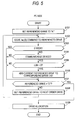
- a drive allocation process (S1) is executed whereby a drive is allocated to an unknown device connected to the PC 3.
- a drive is allocated to the multi-reader/writer 2 that is the sole device connected to the PC 3.
- a drive setting process (S2) is performed where a drive selected by the user is set as a communication target.
- a device the multi-reader/writer 2 in this embodiment
- communication data stored in the RAM 43 is transmitted to the multi-reader/writer 2 (transmission step), and communication data received by the multi-reader/writer 2 is transferred to the liquid crystal display 21 to display the data on the liquid crystal display to perform a transmission/display process (S3).
- a counting unit such as a timer that starts counting on completion of the transmission/display step.
- the procedure from step S3 is repeated.
- the procedure from step S4 is repeated.
- a display erasure process (S7) is performed to erase the information on the liquid crystal display 21, followed by completion of a series of processing.
- the drive allocation process (S1), the drive setting process (S2), the transmission/display process (S3), the process to determine whether the display content must be changed (S6), and the display erasure process (S7) will be respectively detailed.
- step S101 the drive allocation process (S1) performed by the CPU 41 of the PC 3 will be described.
- the process starts with step S101.
- a drive to be referenced (hereinafter referred to as the referenced drive) is initially set to Drive A (S101).
- the referenced drive means a dive that may be allocated by the PC 3.
- a drive is selected in ascending order in the drive allocation step.
- the referenced drive is managed by the OS kernel of the OS 2000 of the PC 3.
- the candidate drives for allocation are A to Z (total 26 drives).
- the Inquiry command (hereinafter referred to as the Inq(0) command) to request the device to which the drive is allocated to return Standard-Inquiry data (hereinafter abbreviated as the S/I data) is issued by the CPU 21 to the referenced drive (S102).
- the Inq(0) command is issued to the OS kernel by the CPU 41 and the OS kernel assumes that the Inq(0) command is issued to the referenced drive.
- Inquiry data with the EVPD area set to "0" (hereinafter referred to as Inq(0) data) is generated by the OS kernel and transmitted to an unknown device associated with the referenced drive.
- the SCSI standard specifies that S/I data be returned in case the EVPD area is set to "0".
- Inq(0) data generated in this embodiment is shown in Table 3.
- step 103 error determination is made by the CPU 41 based on the presence/absence of response of S/I data (S102). In case S/I data is not returned, an error is assumed (Yes in S102). In this case, execution proceeds to step S107. In case S/I data is returned, an error is not assumed (No in S102). In other words, it is determined that a device is present associated with the referenced drive. In this case, execution proceeds to step S105.
- step S103 it is determined whether the device associated with the referenced drive can be a communication target or a communicable device based on the returned S/I data.
- the step is performed to determine whether the device associated with the referenced drive is a multi-reader/writer 2.
- S/I data shown in Table 4 is returned by the multi-reader/writer 2 to the PC 3. Determination in the step is made by checking the data in Byte 0 or 1, the vendor ID of the area of Byte 8 to Byte 15 and product ID of the area of Byte 16 to Byte 31 of the returned S/I data against the ID information pre-registered in the PC 3.
- step S105 In case the device in question is determined as a communicable device in step 5104 (Yes in S104), execution proceeds to step S105. In case the device in question is determined as a non-communicable device in step S104 (No in S104), execution proceeds to step S107.
- the data "0x00" in the area of Byte 0 indicates a direct access device while the data "0x80" in the area of Byte 1 indicates a rewritable storage medium. Content described in each byte area is defined in the SCSI standard. For details, refer to the SCSI standard.
- step S105 whether the LUN of the referenced drive is "0" is determined by the CPU 41 based on the returned S/I data. This determination is made based on the data in the area of Byte 54 in the vendors-specific area in the S/I data.
- S/I data shown in Table 4 is returned from the multi-reader/writer 2 to the PC 3.
- programming is made to store information indicating the physical I/F of the multi-reader/writer 2 (information indicating USB in this embodiment) in the upper 4 bits of the area of Byte 54 and store the LUN number in the lower 4 bits.
- the CPU 41 has only to reference the data in the area of Byte 54 to acquire LUN information. This performs determination in step S105. For example, in case “0x00" is stored in the area of Byte 54, information is acquired indicating that the physical I/F is a USB connector and the LUN is 0. In case “0x23" is stored, information is acquired indicating that the physical I/F is an SCSI connector and the LUN is 3.
- step S105 when the LUN is determined as "0" (Yes in step S105), execution proceeds to step S107.
- step S106 the current referenced drive is added to a corresponding drive list.
- the corresponding drive list is a list of referenced drives to which drives are finally allocated.
- the corresponding drive list is expanded in a predetermined storage area of the RAM 43 and the corresponding referenced drive is written into the storage area. Execution then proceeds to step S107.
- step S107 Whether the referenced drive is Drive Z is determined by the CPU 41. For example, whether the current referenced drive is Drive Z may be determined by counting the drive referencing order on a counter memory and supervising the count value with the CPU 41. Such determination is made to determine whether the referenced drive now specified is the final one. When it is determined that the referenced drive is Drive Z, no further drives to be referenced exist, so that execution proceeds to step S109. Otherwise, the referenced drive is set to the next-order drive (S108). The procedure from step S102 is repeated until step S107 ends with Yes.
- drives are allocated based on the corresponding drive list. This terminates a series of drive allocation processes (S1). In this embodiment, only the multi-reader/writer 2 is connected as an external storage device so that the multi-reader/writer 2 is allocated to Drive A, with no devices allocated to the other drives.
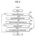
- step S201 the drive setting process (S2) performed by the CPU 41 of the PC 3 will be described.
- the process starts with step S201.
- step S201 whether a drive allocated by the drive allocation process (S1) (hereinafter referred to as the "corresponding drive”) is present is determined (S201). That is, whether a predetermined device is allocated to any one of the drives that accepts allocation on the PC 3 is determined.
- Drive A is present where the multi-reader/writer 2 is allocated so that it is determined that a corresponding drive is present.
- S202 whether only one corresponding drive is present is determined (S202). In case it is determined that the corresponding drive is absent in step S202 (No in S201), no communication targets are present thus terminating the process. In this case, clock data or message data stored in the RAM 43 is not transmitted.
- the corresponding drive is set as a communication target (S205). That is, a device associated with the corresponding drive is set as a communication target.
- Drive A is set as a communication target.
- the multi-reader/writer 2 is set as a communication target device.
- the transmission/display process (S3) is performed between the multi-reader/writer 2 set as a communication target in the drive setting process (S2) and the PC 3.
- the process starts with step S301.
- the Inquiry command used to request the multi-reader/writer 2 to return the VPD (Vital Product Data) on the multi-reader/writer 2 (hereinafter referred to as the Inq(1) command) is issued to Drive A (step S301).
- the Inq(1) command is issued to the OS kernel and the OS kernel assumes that the Inq(0) command is issued to Drive A.
- Inquiry data with the EVPD area set to "1" (hereinafter referred to as Inq(1) data) is generated by the OS kernel and transmitted to the multi-reader/writer 2 associated with Drive A via the USB cable 25.
- the Inq(1) data generated is shown in Table 5.
- Table 5 a page code "0xE0" is described in the area of Byte 2 of the Inq(1) data.
- the SCSI standard specifies that VPD be returned in case the EVPD area is set to "1".
- the allocation length area stores a data length required of the connected device.
- the maximum value of the allocation length of the multi-reader/writer 2 is preset to a fixed length of 15 bytes.
- the numeral "15" may be represented by the lower 4 bits. According to the SCSI standard, even when a numeric value exceeding the maximum value set by the multi-reader/writer 2 is specified as an allocation length, The allocation length of the multi-reader/writer 2 is set to the maximum value or 15 bytes.
- the allocation length is set to 15 bytes.
- data in the allocation length area may be used as arbitrary data without limitation.
- data communications are performed between a PC 3 and a multi-reader/writer 2 by adding arbitrary communication data to the reserved free area.
- the allocation length is not necessarily set to a fixed length of 15 bytes.
- the maximum value of the allocation length may be set in accordance with the page code of Inq(1) data. For example, the maximum value of the allocation length is set to a fixed length of 15 bytes in case the page code is "0xE0".
- the maximum value of the allocation length is set to a fixed length of 9 bytes in case the page code is "0xE2". This setting process is made as the content of the page code is read by the CPU 27 of the multi-reader/writer 2 that has received Inq(1) data and a corresponding fixed length is selected from a fixed length corresponding list previously stored in the ROM 28.
- the allocation length set to 15 bytes or 9 bytes may be arbitrarily set.
- Tables 6 and 7 show classified communication data added to a free area reserved in the allocation length area. As shown in the data description column of each table, each data item has a definition of what the data item means. For details, refer to the description in the data description column. Table 6 shows communication data transmitted in case in case the page code is "0xE0". Table 7 Table 6 shows communication data transmitted in case in case the page code is "0xE2". Table 6: Page code: 0xE0 Allocation area data Data description 0x00 - 0x0F (00000000) - (00001111) Allocation length 0x10 (0007.0000) Acquires switch content.
- 0x11 (00010001) Transfers to the liquid crystal display the data stored in the character string storage area of a character string number of next transmit data (0x80-0xFF). 0x1F (00011111) Cancels processing while waiting for next transmit data.
- Table 7 Page code: 0xE2 Allocation area data Data description 0x00 - 0x09 (00000000)-(00001001) Allocation length 0x0a - 0x0F (00001010)-(00001111) Text data 0x20 - 0x0FF (00100000)-(11111111) Text data 0x10 (00010000) Stores 0x00 into the character string storage area of the device 0x11 (00010001) Stores into the character string storage area of the device a value obtained by subtracting 0x20 from next transmit data (0x20-0x3F).
- the left column shows data described in the allocation length area while the right column shows the meaning of the data.
- the multi-reader/writer 2 uses the CPU 27 to extract the data in the allocation length area from the received Inq(1) data, analyzes the content of extracted data, and performs processing in accordance with the analysis result.
- Data in Tables 6 are 7 is previously stored in the HDD 44 or ROM 42 of the PC 3 and Rom 28 of the multi-reader/writer 2 in a table list format.
- Inq(1) data generated when the Inq(1) command was issued in step S301 has "0x10" described in the allocation length area as shown in Table 5.
- the Inq(1) command is a command issued by the PC 3 to request the multi-reader/writer 2 to read the switch position.
- the multi-reader/writer 2 receives the transmitted Inq(1) data. Then the data "0x10" in the allocation length area in the Inq(1) data is extracted by the CPU 27 and the position of the selector switch 22 is detected in accordance with the data (S302).
- the detection result is returned by the CPU 27 to the PC 3 (S303).
- the return processing is made by writing the detection result into the VPD (refer to Table 8) generated after receipt of Inq(1) data and returned to the PC 3.
- VPD VPD
- detection result of the switch position is written into the area of Byte 7.
- Table 8 shows the VPD assumed in case the switch is in Position B.
- Table 8 VPD (Inq(1) data reception) Byte Data Remarks 0 0x00 Direct access device 1 0xE0 Page code 2 0x00 Reserved (fixed to 0) 3 0x0B Byte 15 (0-15) present 4 nn Version information of device 5 0x00 Fixed to 0 6 nn (Unused) 7 0x01 Switch position 8-14 nn (Unused)
- the PC 3 receives VPD returned from the multi-reader/writer 2 and references the area of Byte 7 of the VPD to determine in which contact, A or B, the switch is positioned.
- the selector switch 22 is in Position A (A in S304)
- the current clock data is generated and is stored into the RAM 43 (S305).
- the selector switch 22 is in Position B (B in S304)
- a message data item previously selected by the user is selected out of the plural message data items stored in the RAM 43 (S306).
- a transmission process is performed where The clock data or selected message data item stored in the RAM 43 is read and the data is transmitted to the multi-reader/writer 2 (S307).
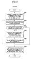
- This transmission process is performed in accordance with the procedure on and after step S401 shown in the flowchart of Fig. 8. That is, the Inq(1) command is issued (step S401). Inq(1) data generated when the Inq(1) command is issued is transmitted to the multi-reader/writer 2. VPD is returned from the XXX 2 on issuance of the Inq(1) command, without return data added to the VPD. Thus, the VPD return processing will not be described.
- step S401 Inq(1) data is generated where "0xE2" is described as a page code in the area of Byte 2 and "0x18" is described in the allocation length area.
- the Inq(1) command issued in step S401 is a request command to set a pointer at the head of the character string storage area (storage area in the RAM 29) corresponding to the character string number shown by "0x90" according to Table 7. This request command is issued to the multi-reader/writer 2.
- the pointer means an indicator to indicate the position where a character segmented in step S402 is stored as described later.
- step S402 characters are segmented in order from the top of character string data indicating a time or a message stored in the RAM 43 of the PC 3. Whether a character segmented in step S402 is a terminating character is determined by the CPU 41 (S403). This processing is determined based on whether the data indicating a segmented character is "0x00". Because "0x00" does not indicate a character, in case it is determined that the data is "0x00", the segmented character is determined to be a terminating character. When the segmented character is determined to be a terminating character, execution proceeds to step S406. In case it is determined that the segmented character is not a terminating character, execution proceeds to step S404.
- step S404 When execution proceeds to step S404, the Inq(1) command is issued and Inq(1) data is generated where "0xE2" is described as a page code and "output character" is described in the allocation length area.
- the generated Inq(1) data is transmitted to the multi-reader/writer 2.
- the output character means data to indicate a character segmented in step S402, for example data represented in an ASCII code.
- step S406 the Inq(1) command is issued and Inq(1) data is generated where "0xE2" is described as a page code in the area of Byte 2 and "0x17" is described in the allocation length area.
- This is a request command to pad all bit areas with "0x00" starting with the area where the last character (end character) is stored.
- this is a request command to append "0x00" to the end of data transmitted to the multi-reader/writer 2 and stored into the RAM 29 to align the stored data to bit data of a predetermined length (for example 128 bytes).
- the transmission processing (S307) is complete.
- step S307 When data is transmitted by way of the transmission processing (S307), the transmitted data is received by the multi-reader/writer 2 and the received data is stored into the RAM 29 (S308).
- step S406 each time a character segmented in step S406 (refer to Fig. 8) is transmitted, its character data is sequentially stored into the RAM 29.
- step 5309 the Inq (1) command is issued by the PC 3 again.
- the Inq (1) data generated on that occasion is transmitted to the multi-reader/writer 2 (5309).
- the Inq(1) data generated on that occasion is shown in Table 9.
- Table 9 "0xE0" is described in the area of Byte 2 and "0x11" is described in the allocation length area. From Table 6, it is understood that the issued Inq(1) command is a request command to transfer data stored in the character string storage area (storage area in the RAM 29) of a character string number corresponding to the number shown by the next data to transmit, to the liquid crystal display 21 of the multi-reader/writer 2.
- the Inq(1) command is issued again.
- the Inq(1) data is transmitted to the multi-reader/writer 2 where "0xE0" is described as a page code in the area of Byte 2 and character data is described in the allocation length area (S310).
- receive data character data stored in the character string storage area corresponding to a character string number transmitted in step S310 is read by the CPU 27 and the receive data is transferred to the liquid crystal display 21. This causes the data from the PC 3 to be displayed on the liquid crystal display 21.
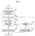
- step S6 the determination process (S6) to determine whether the display content must be changed will be described using the flowchart of Fig. 9.
- the determination process is performed by the CPU 41 of the PC 3. This process starts with step S501.
- step S501 same as step S301, the Inq(1) command is issued.
- the Inq(1) data generated on that occasion is transmitted to the multi-reader/writer 2 to detect the position of the selector switch 22.
- step S502 whether the switch position has changed is determined. This processing is made by previously storing the switch position detected in step S301 into the RAM 29 and comparing the stored switch position information with the switch position detected in step S501. When it is determined that the switch contact has changed by the user's operation to toggle the switch, it is determined that the display content must be changed (S507). Otherwise, the switch position information stored in the RAM 29 is read in step S502 and the current switch position is confirmed.
- step S506 whether the time has changed in minutes since clock data was generated in step S305 is determined based on the clock function of the PC 3. In case it is determined that the time has changed, it is determined that the display content must be changed (S507). Otherwise, it is determined that the display content need not be changed (S505).
- whether the time has changed in minutes since clock data was generated in step S305 is determined based on the clock function of the PC 3. In case it is determined that the time has changed, it is determined that the display content must be changed (S507). Otherwise, it is determined that the display content need not be changed (S505).
- step S7 the display erasure process (S7) will be described using the flowchart of Fig. 10. The process starts with step S601.
- step S601 In case it is determined that an end instruction is input in step S5 (refer to Fig. 4), the Inq(1) command is issued in step S601.
- the Znq(1) data generated on that occasion is transmitted to the multi-reader/writer 2 (S601).
- the Inq(1) data generated on that occasion is has "0xE0" described in the area of Byte 2 and "0x11" described in the allocation length area. From Table 6, it is understood that the issued Inq(1) command is a request command to transfer data stored in the character string storage area of a character string number indicated by the next data to transmit, to the liquid crystal display 21 of the multi-readez/writer 2.
- step S602 the Inq(1) command is issued.
- the Inq(1) data is generated and transmitted where "0xE0" is described in the area of Byte 2 and "0x80" is described in the allocation length area.
- the character string storage area of a character string number indicated by “0x80” is previously reserved as vacant data. This causes the CPU 27 of the multi-reader/writer 2 to transfer the vacant data in the character string storage area of the character string number indicated by "0x80" to the liquid crystal display and the display content is erased.
- Data communications are performed in accordance with the above procedure in this embodiment. For example, even in case a memory card is replaced with another, it is possible to transfer clock data and message data from the PC 3 to the multi-reader/writer 2 while the multi-reader/writer 2 is retaining its replacement information. It is also possible to transfer the switch position information on the selector switch from the multi-reader/writer 2 to the PC 3. Even in case the multi-reader/writer 2 is in the Not Ready state where an SCSI command from the PC 3 is rejected because the driver software for the multi-reader/writer is not installed, data communications between the PC 3 and the multi-reader/writer 2 are assured. While clock data, message data and switch position information are described as data to be communicated in this embodiment, data to be communicated in this invention is not limited thereto.
- Fig. 11 is a schematic external view of a multi function device 80.
- the multi function device 80 integrally includes a printer 82 arranged in a lower part, a scanner 83 arranged above the printer 82, a manuscript cover 86 equipped with an ADF 86, an operation panel 85 arranged on the front side of the top surface of the device, and a multi-reader/writer 88 arranged so as to expose a slot on the front surface of the device, and has a printer function, a scanner function, a copy function, and a facsimile function.
- the multi function device 80 is connected to a PC 3 (refer to Fig. 3) mainly described in the first embodiment and records images or documents on recording paper on the printer 82 based on print data including image data and document data transmitted from the PC 3.
- the printer 82 may record images or documents on recording paper based on the print data read by the multi-reader/writer 88 from a memory card. Further, the printer 82 works as a reader/writer device to perform data communications with a memory card inserted into the multi-reader/writer 88.
- the printer 82 also transmits image data read by the scanner 83 to the PC 3 or makes thereon a copy of an image read by the scanner 83.
- the multi-reader/writer 88 of the multi function device 80 includes a first slot 16, a second slot 17, a third slot 18 and a fourth slot 19. Configuration and function of each slot and a memory card inserted into each slot are same as those on the multi-reader/writer 2 in the first embodiment except that the third slot 18 and the fourth slot 19 are integrated.
- the multi-reader/writer 88 includes a liquid crystal display 21 and a selector switch 22 mounted on its front surface where the slots are arranged. Configuration and function of the liquid crystal display 21 and the selector switch 22 are the same as those in the first embodiment. Thus, a same component as in the first embodiment is given the same sign as the first embodiment and the detailed description is omitted.
- the multi function device 80 thus configured and the PC 3 are interconnected to provide a similar communication system to that in the first embodiment. Even in case the multi function device 80 is in the Not Ready state where it rejects an SCSI command from the PC 3, data communications between the PC 3 and the multi function device 80 are assured.
- the peripheral device when the Inquiry data is received, the peripheral device returns VPD (Vital Product Data) to the information processing device depending on the content of the Inquiry data.
- VPD Vital Product Data
- the current SCSI standard specifies that the EVPD area be composed of a single bit string.
- the EVPD area is set to "0" before acquiring the configuration information of a peripheral device.
- the SCSI standard describes that, in case "1" is set to the EVPD area, an optional feature works to transfer VPD information from a peripheral device to an information processing device. However, it is empirically known that the optional feature rarely used in reality.
- the invention adds communication data to the free area in case "1" is set to the EVPD area. This discriminates between a case where the configuration information of a peripheral device is acquired using Inquiry data and a case where data communications are made.
- the current SCSI standard specifies that the allocation length area is composed of an 8-bit string or a 16-bit string.
- This area is used to describe the data length of a memory area for storing data into a recording medium inserted into a peripheral device.
- the area has a larger bit width than other areas and may be modified, so that it is preferable as an area to add communication data.
- the maximum numeric value information described therein is (255) 10 in decimals and (OxFF) 16 in hexadecimals.
- the allocation length allocated to the recording medium is a smaller numeric value than (255) 10
- a numeric value larger than the numeric value is not used as information indicating an allocation length.
- This unused area is preferably used as a free area.
- the allocation length area is an 8-bit string and the allocation length for the peripheral device is preset to (127) 10 in decimals
- the value (127) 10 may be expressed in seven bits so that seven bits of the allocation length area are used to represent (127) 10 .
- the remaining one bit is left unused. In this case, by efficiently using the remaining one bit, it is possible to reserve a free area of maximum 7 bits in the allocation length area.
Landscapes
- Engineering & Computer Science (AREA)
- Theoretical Computer Science (AREA)
- Physics & Mathematics (AREA)
- General Engineering & Computer Science (AREA)
- General Physics & Mathematics (AREA)
- Information Transfer Systems (AREA)
- Information Retrieval, Db Structures And Fs Structures Therefor (AREA)
- Information Transfer Between Computers (AREA)
- Computer And Data Communications (AREA)
- Communication Control (AREA)
Applications Claiming Priority (1)
| Application Number | Priority Date | Filing Date | Title |
|---|---|---|---|
| JP2005272379A JP4622770B2 (ja) | 2005-09-20 | 2005-09-20 | 通信システム、情報処理装置、周辺装置、及び通信方法 |
Publications (3)
| Publication Number | Publication Date |
|---|---|
| EP1770538A2 true EP1770538A2 (de) | 2007-04-04 |
| EP1770538A3 EP1770538A3 (de) | 2007-05-02 |
| EP1770538B1 EP1770538B1 (de) | 2008-11-19 |
Family
ID=37801646
Family Applications (1)
| Application Number | Title | Priority Date | Filing Date |
|---|---|---|---|
| EP06254877A Ceased EP1770538B1 (de) | 2005-09-20 | 2006-09-20 | SCSI-Kommunikationssystem, Informationsverarbeitungsvorrichtung, Peripheriegerät und Kommunikationsverfahren |
Country Status (5)
| Country | Link |
|---|---|
| US (1) | US8051221B2 (de) |
| EP (1) | EP1770538B1 (de) |
| JP (1) | JP4622770B2 (de) |
| CN (1) | CN100447733C (de) |
| DE (1) | DE602006003711D1 (de) |
Cited By (1)
| Publication number | Priority date | Publication date | Assignee | Title |
|---|---|---|---|---|
| CN111611018A (zh) * | 2020-05-28 | 2020-09-01 | 广州市金库物联科技有限公司 | 用于兼容多型号uhf读写器的方法、终端系统及设备 |
Families Citing this family (4)
| Publication number | Priority date | Publication date | Assignee | Title |
|---|---|---|---|---|
| CN101751353A (zh) * | 2009-12-24 | 2010-06-23 | 深圳华为通信技术有限公司 | 数据卡升级方法及装置 |
| US8977879B2 (en) * | 2012-03-30 | 2015-03-10 | Motorola Solutions, Inc. | Method and apparatus for enhancing a multi-stage hibernate and resume process |
| CN103605632B (zh) * | 2013-11-18 | 2016-06-29 | 山东大学 | 一种axi总线与ahb总线的通信方法与装置 |
| JP2018136803A (ja) * | 2017-02-23 | 2018-08-30 | 株式会社日立製作所 | 画像認識システム |
Family Cites Families (24)
| Publication number | Priority date | Publication date | Assignee | Title |
|---|---|---|---|---|
| JPH05216592A (ja) * | 1991-04-30 | 1993-08-27 | Internatl Business Mach Corp <Ibm> | 記憶装置識別方法及び遠隔記憶システム |
| US5892955A (en) * | 1996-09-20 | 1999-04-06 | Emc Corporation | Control of a multi-user disk storage system |
| JP2868001B1 (ja) | 1997-09-01 | 1999-03-10 | 日本電気株式会社 | ディスクアレイ装置制御方法およびディスクアレイ装置 |
| JP2000227868A (ja) * | 1998-12-04 | 2000-08-15 | Hitachi Ltd | バックアップ取得方法および計算機システム |
| JP3800903B2 (ja) * | 2000-02-17 | 2006-07-26 | 株式会社日立製作所 | 記憶装置及びそのアクセス制御方法 |
| JP2002049534A (ja) * | 2000-07-31 | 2002-02-15 | Rexas Inc | バックアップ/リストアシステム、バックアップ装置およびバックアップ/リストア方法 |
| JP2002077690A (ja) | 2000-08-31 | 2002-03-15 | Olympus Optical Co Ltd | 電子カメラおよびコンピュータシステム |
| JP2002109528A (ja) | 2000-09-26 | 2002-04-12 | Funai Electric Co Ltd | データ記憶装置 |
| US7039727B2 (en) | 2000-10-17 | 2006-05-02 | Microsoft Corporation | System and method for controlling mass storage class digital imaging devices |
| US6895453B2 (en) * | 2001-03-15 | 2005-05-17 | International Business Machines Corporation | System and method for improved handling of fiber channel remote devices |
| US7385635B2 (en) | 2001-04-24 | 2008-06-10 | Nikon Corporation | Electronic image processing device and system for image data transfer operation |
| JP4569032B2 (ja) | 2001-04-24 | 2010-10-27 | 株式会社ニコン | 電子機器および電子機器システム |
| RU2004130859A (ru) | 2002-09-06 | 2005-06-10 | Макстор Корпорейшн (Us) | Внешнее устройство резервного копирования, управляемое одной кнопкой |
| US7003589B2 (en) * | 2002-10-01 | 2006-02-21 | Hewlett-Packard Development Company, L.P. | Method and arrangement for generating unique identifiers for logical units of SCSI devices |
| JP2004215164A (ja) * | 2003-01-08 | 2004-07-29 | Seiko Epson Corp | 外部機器制御装置、外部機器制御方法および外部機器制御プログラム |
| US7526580B2 (en) | 2003-06-27 | 2009-04-28 | Brother Kogyo Kabushiki Kaisha | Peripheral device |
| JP4023402B2 (ja) | 2003-06-27 | 2007-12-19 | ブラザー工業株式会社 | 周辺装置 |
| JP4062227B2 (ja) | 2003-09-30 | 2008-03-19 | ブラザー工業株式会社 | 周辺装置及び画像形成装置 |
| US7257573B2 (en) * | 2003-07-29 | 2007-08-14 | Matsushita Electric Industrial Co., Ltd. | Information display apparatus |
| JP2005050192A (ja) | 2003-07-30 | 2005-02-24 | Matsushita Electric Ind Co Ltd | 情報記録システム |
| US7085867B2 (en) * | 2003-08-06 | 2006-08-01 | Lsi Logic Corporation | Methods and structure for SCSI2 to SCSI3 reservation protocol mapping |
| JP4033085B2 (ja) | 2003-09-02 | 2008-01-16 | ブラザー工業株式会社 | 画像読取装置およびそれを備えた複合機 |
| US7506078B2 (en) * | 2004-10-29 | 2009-03-17 | Intel Corporation | Integrated circuit capable of assigning a unique identity to ATA/ATAPI devices |
| US7840755B2 (en) * | 2005-05-24 | 2010-11-23 | Lsi Corporation | Methods and systems for automatically identifying a modification to a storage array |
-
2005
- 2005-09-20 JP JP2005272379A patent/JP4622770B2/ja not_active Expired - Fee Related
-
2006
- 2006-09-19 US US11/533,078 patent/US8051221B2/en not_active Expired - Fee Related
- 2006-09-20 CN CNB2006101389544A patent/CN100447733C/zh not_active Expired - Fee Related
- 2006-09-20 EP EP06254877A patent/EP1770538B1/de not_active Ceased
- 2006-09-20 DE DE602006003711T patent/DE602006003711D1/de active Active
Cited By (1)
| Publication number | Priority date | Publication date | Assignee | Title |
|---|---|---|---|---|
| CN111611018A (zh) * | 2020-05-28 | 2020-09-01 | 广州市金库物联科技有限公司 | 用于兼容多型号uhf读写器的方法、终端系统及设备 |
Also Published As
| Publication number | Publication date |
|---|---|
| US20070094424A1 (en) | 2007-04-26 |
| CN100447733C (zh) | 2008-12-31 |
| JP2007086905A (ja) | 2007-04-05 |
| DE602006003711D1 (de) | 2009-01-02 |
| EP1770538B1 (de) | 2008-11-19 |
| CN1936821A (zh) | 2007-03-28 |
| US8051221B2 (en) | 2011-11-01 |
| JP4622770B2 (ja) | 2011-02-02 |
| EP1770538A3 (de) | 2007-05-02 |
Similar Documents
| Publication | Publication Date | Title |
|---|---|---|
| US7007127B2 (en) | Method and related apparatus for controlling transmission interface between an external device and a computer system | |
| US6757783B2 (en) | Portable storage medium based on universal serial bus standard and UFI standard | |
| US7797398B2 (en) | Communication system, and peripheral device having trigger generating device and computer program product that monitors whether a trigger has been generated | |
| US7941579B2 (en) | Communication system for authenticating authority of host device for accessing storage medium set to periphery device | |
| US7412558B2 (en) | Semiconductor storage device | |
| US7162549B2 (en) | Multimode controller for intelligent and “dumb” flash cards | |
| CN100541529C (zh) | 存储卡、数据写入设备和包括所述存储卡的系统 | |
| US6378033B1 (en) | Electronic device, control method thereof and storage medium | |
| CN101101584A (zh) | 卡式外围装置和主机装置 | |
| US6941397B2 (en) | Quick save system and protocol, monitor program and smart button firmware of the same | |
| US7869074B2 (en) | Communication system, information processing device, peripheral device and communication method | |
| EP1770538B1 (de) | SCSI-Kommunikationssystem, Informationsverarbeitungsvorrichtung, Peripheriegerät und Kommunikationsverfahren | |
| US7014121B2 (en) | Method of self-detecting and dynamically displaying detected results for a card reader used to read flash memory cards | |
| US7249710B2 (en) | Method of dynamic icons and labels showing status of the memory card in a card reader | |
| JP3914949B2 (ja) | Usbストレージデバイス、その制御装置及びその制御装置に実行させるためのプログラム | |
| JP2005018645A (ja) | 周辺装置 | |
| US20070174516A1 (en) | Adaptor | |
| JP4618560B2 (ja) | 通信システム及びそれに使用する周辺装置 | |
| US7810737B2 (en) | Record reproduction apparatus, record reproduction method, record reproduction program, storage medium, and information storage medium | |
| CN100520756C (zh) | 管理存储卡插入或拔出读卡器的方法和所述方法中使用的设备 | |
| JP3858747B2 (ja) | Pcカードアダプタ | |
| KR101120028B1 (ko) | 이동식 디스크 드라이브 구성 방법 및 멀티 메모리카드리더기를 구비하는 프린터 | |
| JP4807667B2 (ja) | 通信システム及びそれに使用する周辺装置 | |
| JP2007265305A (ja) | 通信システム及びそれに使用する周辺装置 | |
| CN201081782Y (zh) | 电子信号转换装置 |
Legal Events
| Date | Code | Title | Description |
|---|---|---|---|
| PUAI | Public reference made under article 153(3) epc to a published international application that has entered the european phase |
Free format text: ORIGINAL CODE: 0009012 |
|
| PUAL | Search report despatched |
Free format text: ORIGINAL CODE: 0009013 |
|
| AK | Designated contracting states |
Kind code of ref document: A2 Designated state(s): AT BE BG CH CY CZ DE DK EE ES FI FR GB GR HU IE IS IT LI LT LU LV MC NL PL PT RO SE SI SK TR |
|
| AX | Request for extension of the european patent |
Extension state: AL BA HR MK YU |
|
| RIC1 | Information provided on ipc code assigned before grant |
Ipc: G06F 13/12 20060101AFI20070223BHEP Ipc: G06F 13/42 20060101ALI20070321BHEP |
|
| RTI1 | Title (correction) |
Free format text: SCSI COMMUNICATION SYSTEM, INFORMATION PROCESSING DEVICE, PERIPHERAL DEVICE AND COMMUNICATION METHOD |
|
| AK | Designated contracting states |
Kind code of ref document: A3 Designated state(s): AT BE BG CH CY CZ DE DK EE ES FI FR GB GR HU IE IS IT LI LT LU LV MC NL PL PT RO SE SI SK TR |
|
| AX | Request for extension of the european patent |
Extension state: AL BA HR MK YU |
|
| 17P | Request for examination filed |
Effective date: 20071029 |
|
| AKX | Designation fees paid |
Designated state(s): DE FR GB |
|
| GRAP | Despatch of communication of intention to grant a patent |
Free format text: ORIGINAL CODE: EPIDOSNIGR1 |
|
| GRAS | Grant fee paid |
Free format text: ORIGINAL CODE: EPIDOSNIGR3 |
|
| GRAA | (expected) grant |
Free format text: ORIGINAL CODE: 0009210 |
|
| AK | Designated contracting states |
Kind code of ref document: B1 Designated state(s): DE FR GB |
|
| REG | Reference to a national code |
Ref country code: GB Ref legal event code: FG4D |
|
| REF | Corresponds to: |
Ref document number: 602006003711 Country of ref document: DE Date of ref document: 20090102 Kind code of ref document: P |
|
| PLBE | No opposition filed within time limit |
Free format text: ORIGINAL CODE: 0009261 |
|
| STAA | Information on the status of an ep patent application or granted ep patent |
Free format text: STATUS: NO OPPOSITION FILED WITHIN TIME LIMIT |
|
| 26N | No opposition filed |
Effective date: 20090820 |
|
| REG | Reference to a national code |
Ref country code: FR Ref legal event code: PLFP Year of fee payment: 11 |
|
| REG | Reference to a national code |
Ref country code: FR Ref legal event code: PLFP Year of fee payment: 12 |
|
| REG | Reference to a national code |
Ref country code: FR Ref legal event code: PLFP Year of fee payment: 13 |
|
| PGFP | Annual fee paid to national office [announced via postgrant information from national office to epo] |
Ref country code: IT Payment date: 20180823 Year of fee payment: 11 |
|
| PGFP | Annual fee paid to national office [announced via postgrant information from national office to epo] |
Ref country code: GB Payment date: 20180919 Year of fee payment: 13 |
|
| PGFP | Annual fee paid to national office [announced via postgrant information from national office to epo] |
Ref country code: DE Payment date: 20190910 Year of fee payment: 14 |
|
| GBPC | Gb: european patent ceased through non-payment of renewal fee |
Effective date: 20190920 |
|
| PG25 | Lapsed in a contracting state [announced via postgrant information from national office to epo] |
Ref country code: GB Free format text: LAPSE BECAUSE OF NON-PAYMENT OF DUE FEES Effective date: 20190920 |
|
| REG | Reference to a national code |
Ref country code: DE Ref legal event code: R119 Ref document number: 602006003711 Country of ref document: DE |
|
| PG25 | Lapsed in a contracting state [announced via postgrant information from national office to epo] |
Ref country code: DE Free format text: LAPSE BECAUSE OF NON-PAYMENT OF DUE FEES Effective date: 20210401 Ref country code: FR Free format text: LAPSE BECAUSE OF NON-PAYMENT OF DUE FEES Effective date: 20190930 |