EP1770519A2 - Informationsverarbeitungsgerät und dessen Datenverarbeitungsverfahren mit Funktion zur Bildung einer Deskriptor-Warteschlange - Google Patents
Informationsverarbeitungsgerät und dessen Datenverarbeitungsverfahren mit Funktion zur Bildung einer Deskriptor-Warteschlange Download PDFInfo
- Publication number
- EP1770519A2 EP1770519A2 EP06015235A EP06015235A EP1770519A2 EP 1770519 A2 EP1770519 A2 EP 1770519A2 EP 06015235 A EP06015235 A EP 06015235A EP 06015235 A EP06015235 A EP 06015235A EP 1770519 A2 EP1770519 A2 EP 1770519A2
- Authority
- EP
- European Patent Office
- Prior art keywords
- descriptor
- task
- queues
- memory
- data
- Prior art date
- Legal status (The legal status is an assumption and is not a legal conclusion. Google has not performed a legal analysis and makes no representation as to the accuracy of the status listed.)
- Withdrawn
Links
Images





Classifications
-
- G—PHYSICS
- G06—COMPUTING OR CALCULATING; COUNTING
- G06F—ELECTRIC DIGITAL DATA PROCESSING
- G06F9/00—Arrangements for program control, e.g. control units
- G06F9/06—Arrangements for program control, e.g. control units using stored programs, i.e. using an internal store of processing equipment to receive or retain programs
- G06F9/46—Multiprogramming arrangements
- G06F9/48—Program initiating; Program switching, e.g. by interrupt
- G06F9/4806—Task transfer initiation or dispatching
- G06F9/4843—Task transfer initiation or dispatching by program, e.g. task dispatcher, supervisor, operating system
Definitions
- the changing section 120 when the changing section 120 has received the above-mentioned load request from the CPU 100, the changing section 120 reads a task program designated by the CPU 100 from the memory 130 and loads it into the internal memory of the PLD 110. As a result, the PLD 110 changes its internal circuit to perform a task upon the task data using the received task program. After the task is completed, the PLD 110 generates an interrupt signal and transmits it to the CPU 100. Then, the CPU 100 again determines the next task to be carried out by the PLD 110. As a result, when the next task is the same as the one carried out immediately before by the PLD 110, the CPU 100 transmits the next task data to the PLD 110.
- a data-array type processor whose data path can be changed by using programs is known to correspond to the PLD 110 of the information processing apparatus of Fig. 8 (see: JP-2001-312481 A , JP-2003-196246 A , and Hideharu Amano, Akiya Jouraku and Kenichiro Anjo, "A dynamically adaptive switch fabric on a multicontext reconfigurable device", Proceeding of International Field Programmable Logic and Application Conference, pp.161-170, September 2003 ).
- the stream processor when a plurality of task data are processed by using a plurality of corresponding task programs, the task data are not always sorted out for each of the task programs. Therefore, if the stream processor processes the task data on a first-in, first-out basis, the loading operations of task programs from the memory into the internal instruction memory of the array-type processor unit and the saving operations of task programs from the internal instruction memory of the array-type processor unit are frequently carried out, so that the throughput of the stream processor would be decreased and the apparatus would not exhibit a sufficient performance ability.
- the descriptor queue forming unit 6 can be deleted, if the CPU 1 can perform the function of the descriptor queue forming unit 6 by using programs stored in the memory 3.
- the CPU 1 forms descriptors, descriptor columns and descriptor queues.
- the DMA controller 27 loads a task loading program LOAD PRG, a task program TASK PRG or intermediate data INTDA1 from the memory 3 into the array-type processor unit 23 upon receipt of an index IDX from the array-type processor unit 23. Also, the DMA controller 27 reads or saves intermediate data INTDA2 from the array-type processor unit 23 to the memory 3 upon receipt of an index IDX from the array-type processor unit 23. In this case, the DMA controller 27 transmits a destination address WRADR (or a source address RDADR) pointing to a start address of the internal memory of the array-type processor unit 23 along with a transmission data length LENGTH to the array-type processor unit 23.
- WRADR or a source address RDADR
- the input DMA circuit 21 reads a descriptor DSC. Then, a task program TASK PRG is loaded from the memory 3 via the DMA controller 27 into the array-type processor unit 23 in accordance with the read descriptor DSC, while task data TDA is supplied from the memory 3 via the input DMA circuit 21 and the input FIF0 24 to the array-type processor unit 23. Then, the array-type processor unit 23 performs a task upon the task data TDA by the task program TASK PRG. Finally, output data OUT processed by the array-type processor unit 23 is returned via the output FIFO 25 and the memory access control circuit 26 to the memory 3.
- One descriptor DSC is generated by the descriptor queue forming unit 6 or the CPU 1 which is operated in accordance with programs stored in the memory 3. Note that one descriptor DSC is always formed for each task data TDA.
- one descriptor DSC is divided into fields defined by an interrupt flag INT, a type TYPE, a transaction identifier TID, an input data (task data) size ISIZE, a task command TASKCMD, a return (output data) address RADR, and an input data address IADR.
- the interrupt flag INT is a bit used for informing a completion of processing by the stream processor 5 to the CPU 1.
- the transaction identifier TID is an identifier for identifying descriptors DSC from each other, i.e., input data (task data) TDA processed by the array-type processor unit 23.
- the transaction identifier TID along with the task data TDA is supplied from the memory 3 via the input FIF0 24 to the array-type processor unit 23, and the transaction identifier TID along with output data OUT is output from the array-type processor unit 23 via the output FIFO 25 and the memory access control circuit 26 to the memory 3.
- the task command TASKCMD is an indicator for indicating a task carried out by the stream processor 2.
- the input DMA circuit 21 has a descriptor pointer (not shown) for pointing to an address of the memory 3 from which one descriptor DSC is stored.
- the descriptor pointer is set by the CPU 1 using a program stored in the memory 3.
- a start address of a descriptor DSC corresponding to task data TDA to be processed is set by the CPU 1 in the descriptor pointer of the input DMA circuit 21.
- the input DMA circuit 21 reads one descriptor DSC from the memory 3 in accordance with the value of the descriptor pointer so that task data TDA having an input data size ISIZE indicated by the input data address IADR is read by the input DMA circuit 21 from the memory 3 to the input FIFO 24. Also, the transaction identifier TID, the task command TASKCMD and the task data size ISIZE are extracted from the read descriptor DSC and transmitted via the input FIFO 24 to the array-type processor unit 23.
- the input DMA circuit 21 extracts the transaction identifier TID and the return address RADR from the read descriptor DSC and transmits them to the descriptor supervising table 22 so that a relationship between the transaction identifier TID and the return address RADR is stored in the descriptor supervising table 22.
- the array-type processor unit 23 loads a task program TASK PRG or intermediate data INTDA into the internal memory thereof or carries out a task using the task program TASK PRG
- the input FIFO 24 can input the above-mentioned sets. Therefore, the processing efficiency of the stream processor 2 can be increased.
- the output FIF0 25 sequentially stores output data OUT associated with its transaction identifier TID.
- the output FIFO 25 would not transmit the output data OUT to the memory access control circuit 26.
- the output FIFO 25 would transmit the output data OUT associated with the transaction identifier TID to the memory access control circuit 26.
- the output data 0UT of the array-type processor unit 23 can be sequentially stored in the output FIFO 25 without stopping the operation of the array-type processor unit 23. Therefore, the decrease of processing throughput of the stream processor 2 would be suppressed.
- task data TDA. are sorted out for every task program TASK PRG, so as to perform successive tasks upon successive task data using the same task program TASK PRG.
- the number of loading task programs is decreased, thus enhancing the throughput.
- a plurality of descriptor columns each formed by a plurality of descriptors each corresponding to one of a plurality of task data to be processed with the same task program are formed. Then, such a plurality of descriptor columns each for one of a plurality of task programs are linked to form one descriptor queue.
- each descriptor is defined by only a type TYPE, a task command TASKCMD, an input data address IADR and an input data size ISIZE of Fig. 2 for simplifying the description.
- the input DMA circuit 21 can access the subsequent descriptors by incrementing the descriptor pointer by the data size of one descriptor such as 128 bits. Therefore, in the descriptor columns Q0A or Q0B, when the CPU 1 sets a start descriptor pointer ptrQ0A or ptrQ0B in the descriptor pointer of the input DMA circuit 21, the input DMA circuit 21 can access the subsequent descriptors by renewing the descriptor pointer therein without help of the CPU 1.
- the preceding descriptor column such as Q0A includes its last descriptor DSCAB whose input data address IADR stores a link pointer of the subsequent descriptor column such as Q0B, i.e., ptrQ0B.
- the descriptor column Q0A is linked to the descriptor column Q0B to form a descriptor queue.
- "0" is set in the type TYPE of the last descriptor DSCAB of the descriptor column Q0A where a link pointer is set in the input data address IADR.
- the type TYPE is used for identifying the descriptor DSCAB from the other descriptors.
- the stream processor 2 sequentially reads descriptors from the memory 3 in accordance with the descriptor queue to perform successive tasks upon successive task data, so that the number of loading operations of task programs into the array-type processor unit 23 can be suppressed to enhance the throughput of the stream processor 2. Also, even when a plurality of task programs read to be loaded into the array-type processor unit 23, such task programs can be successively loaded into the array-type processor unit 23 by only one load request from the CPU 1 to the stream processor 2. Therefore, there is no processing for the CPU 100 to operate the PLD 110 to determine whether an operation for loading a task program is required for the next task in the data processing apparatus of Fig. 8. Thus, the processing burden of the CPU 1 for loading task programs can be decreased.
- a descriptor queue area for storing two descriptor queues is provided in the memory 3. That is, while the stream processor 2 carries out a processing in accordance with one of the descriptor queues, the CPU 1 or the descriptor queue forming unit 6 forms the other of the descriptor queues to be carried out by the stream processor 2. For example, while the stream processor 2 carries out a processing in accordance with a descriptor queue Q0, the CPU 1 or the descriptor queue forming unit 6 forms another descriptor queue Q1 to be carried out by the stream processor 2 and stores the descriptor queue Q1 in the memory 3.
- descriptor queue area is provided commonly for the descriptor queue Q0 and Q1; however, two descriptor queue areas can be provided separately for the descriptor queues Q0 and Q1.
- the descriptor queue which the stream processor 2 is now carrying out is determined by a flag FX (not shown) stored in the memory 3 which the CPU 1 or the descriptor queue forming unit 6 can recognize.
- the value of the flag FX is switched from "0" to "1” or vice versa by the CPU 1 every time the CPU 1 receives an interrupt signal such as INT1 for showing a task completion from the stream processor 2.
- the task command of the last descriptor column of the preceding descriptor queue is made to coincide with that of the first descriptor column of the subsequent descriptor queue.
- the CPU 1 sorts out the descriptor column Q1B as a first descriptor column of the descriptor queue Q1 if the descriptor column Q0B is a last descriptor column of the descriptor queue Q0
- the CPU 1 sorts out the descriptor column Q1A as a first descriptor column of the descriptor queue Q1 if the descriptor column Q0A is a last descriptor column of the descriptor queue Q0.
- each descriptor column is sorted out as explained above, so that replacement of a task program is unnecessary at a switching of two descriptor switching queues, the number of switching task programs by the array-type processor unit 23 can be further decreased. Therefore, the throughput of the stream processor 2 and the information processing apparatus incorporating the stream processor 2 can be further improved.
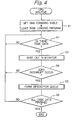
- a flag FX is initialized at a definite value such as "0" and a value LAST TASKCMD is initialized at a definite value by an initial routine (not shown).
- step S1 DMA commands formed by information for writing a task loading program LOAD PRG, task programs TASK PRG and intermediate data INTDA1 into the array-type processor unit 23, information for reading intermediate data INTDA2 from the array-type processor unit 23 and the like are formed and are stored in the DMA controller 27.
- one DMA command is formed to correspond to each process carried out by the DMA controller 27 and is constructed by a read (source) address RDADR showing a start address of a memory area of the memory 3 or the internal memory of the array-type processor unit 23 from which intermediate data or a task program to be transmitted or the like is read; a write (destination) address WRADR showing a start address of a memory area of the memory 3 or the internal memory of the array-type processor unit 23 from which intermediate data or a task program to be transmitted is stored; a transfer data length LENGTH showing a data length of intermediate data or task program to be loaded in the array-type processor unit 23 or a data length of intermediate data to be read or saved from the array-type processor unit 23; a read enable flag RE for showing whether a task program and intermediate data is loaded into the array-type processor unit 23, or intermediate data is read or saved from the array-type processor unit 23; and an interrupt flag DINT showing whether or not generation of an interrupt signal for the CPU 1 is necessary when processing of one DMA command
- step S1 after various kinds of DMA commands are set in the DMA controller 27, one of the DMA commands is indicated to request loading of a task loading program into the array-type processor unit 23.
- the task loading program is used for performing a loading task by which the array-type processor unit 23 loads task programs into the internal memory thereof.
- This loading task also includes a processing for determining whether or not loading of a new task program is required by receiving a task command from the input FIFO 24, and a processing for indicating one of the DMA commands set in the DMA controller 27 in accordance with the received task command from the input FIFO 24.
- step S2 the CPU 1 determines whether or not task data to be processed by the stream processor 2 is present in the memory 3. Only when such task data is present in the memory 3, does the control proceed to step S3 which carries out a sorting-out process for sorting-out descriptors.
- This descriptor sorting-out process is shown in detail in Fig. 5; however, the descriptor sorting-out process can be carried out by the descriptor queue forming unit 6.
- step S4 of Fig. 4 while the CPU 1 carries out a sorting-out process as shown in Fig. 5, the CPU 1 awaits an interrupt signal from the stream processor 2.
- This interrupt signal shows a completion of a loading operation of a task loading program or a completion of a task. Only when the CPU 1 has received such an interrupt signal, does the control proceed to step S5 which forms a descriptor queue by using the descriptor columns Q0x or Q1x.
- This descriptor queue forming process is shown in detail in Fig. 6; however, the queue forming process can be carried out by the descriptor queue forming unit 6.
- interrupt signal at step S4 is an interrupt signal INT1 as illustrated in Fig. 1 generated by the DMA controller 27 when one task is completed or an interrupt signal INT2 as illustrated in Fig. 1 generated by the input DMA circuit 21 when loading of a task loading program into the array-type processor unit 23 is completed.
- step S51 the CPU 1 determines whether the flag FX is "0" or "1".
- the control proceeds to step S52 which forms a descriptor queue Q0 so that the descriptor column having the same task command as the value LAST TASKCMD is at a first position of the descriptor queue Q0.
- the descriptor queue Q0 is stored in the memory 3.
- step S53 the CPU 1 writes "1" into the flag FX and makes the value LAST TASKCMD be the task command value of the last descriptor column of the descriptor queue Q0.
- step S51 when the flag FX is determined to be "1" at step S51, the control proceeds to step S54 which forms a descriptor queue Q1 so that the descriptor column having the same task command as the value LAST TASKCHD is at a first position of the descriptor queue Q1. Then, the descriptor queue Q1 is stored in the memory 3. Then, at step S55, the CPU I writes "0" into the flag FX and makes the value LAST TASKCMD be the task command value of the last descriptor column of the descriptor queue Q1.
- the CPU 1 performs a DMA request operation upon the stream processor 2 by setting the start address of the first descriptor of the descriptor queue Q0 or Q1 into the descriptor pointer of the input DMA circuit 21.
- step S6 of Fig. 4 determines whether the processings for all task data to be processed by the stream processor 2 are finished. As a result, when the processings for all task data are not finished, the control returns to step S2, thus repeating the control at steps S3 to S6. Otherwise, the routine of Fig. 4 is completed.
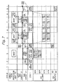
- Fig. 7 the operations of the CPU 1 and the stream processor 2 are illustrated such that the CPU 1 operates the stream processor 2 to carry out tasks A0 to A6 and tasks B0 to B6.
- the tasks A0 to A6 show the processing of a task program A upon task data A0 to A6, respectively
- the tasks B0 to B6 show the processing of a task program B upon task data B0 to B6, respectively.
- descriptors A0 to A6 are formed to correspond to the task data A0 to A6, respectively
- descriptors B0 to B6 are formed to correspond to the task data B0 to B6, respectively.
- a task data and a descriptor corresponding to a task such as A1 are given the same reference as the reference of the task in order to understand the relationship among the tasks, the task data and the descriptors.
- the CPU 1 forms DMA commands for loading a task loading program LOAD PRG and task programs such as A and B.
- the DMA controller 27 when the DMA controller 27 receives the load request from the CPU 1, the DMA controller 27 reads the task loading program LOAD PRG from the memory 3 in accordance with the DMA command designated by the CPU 1, and loads the task loading program LOAD PRG into the array-type processor unit 23. Then, after the loading of the task loading program LOAD PRG into the array-type processor unit 23 is completed, the DMA controller 27 generates an interrupt signal INT for showing the completion of loading the task loading program LOAD PRG and transmits it to the CPU 1.
- the CPU 1 forms descriptors each corresponding to one task data stored in the memory 3 and sorts out the descriptors in accordance with the processing as shown in Fig. 5.
- descriptors A0, A1, B0 and B1 are formed to correspond to task data A0, A1, B0 and B1 stored in the memory 3, and then, a descriptor column Q0A is formed by linking the descriptors A0 and A1 to each other while a descriptor column Q0B is formed by linking the descriptors B0 and B1 to each other.
- the CPU 1 when the CPU 1 receives the interrupt signal INT1 showing the completion of loading the task loading program LOAD PRG from the DMA controller 27, the CPU 1 forms a descriptor queue Q0 by linking the descriptor columns Q0A and Q0B to each other. Then, the CPU 1 writes the start address of the first descriptor column Q0A of the descriptor column Q0 into the descriptor pointer of the input DMA circuit 2, thus starting a data DMA request to read the descriptors A0, A1, B0 and B1.
- the input DMA circuit 21 reads the descriptor (DSC) A0 from the memory 3 in accordance with the value of the descriptor pointer of the input DMA circuit 21, and extracts a task command TASKCMD, a transaction identifier TID and an input data size ISIZE from the descriptor A0 to transmit them via the input FIFO 24 to the array-type processor unit 23. Also, the input DMA circuit 21 reads task data (DTA) A0 designated by the descriptor (DSC) A0 from the memory 3 and transmits the task data A0 via the input FIFO 24 to the array-type processor unit 23.
- DTA task data
- the array-type processor unit 23 determines whether or not a task program A designated by the task command A0 is already loaded thereinto. In this case, since the task program A is not loaded yet, the array-type processor unit 23 generates a load request for the task program A by transmitting index information IDX for indicating a corresponding DMA command to the DMA controller 27.
- the DMA controller 27 reads the task program A from the memory 3 in accordance with the DMA command indicated by the array-type processor unit 23 to transmit the task program A to the array-type processor unit 23.
- the DMA controller 27 completes the loading operation of the task program A, the DMA controller 27 generates a load completion signal CPL and transmits it to the array-type processor unit 23.
- the input DMA circuit 21 reads the descriptor (DSC) A1 and the task data (TDA) A1 following the descriptor A0 and the task data A0 from the memory 3, and extracts a task command TASKCMD, a transaction identifier TID and an input data size ISIZE from the descriptor A1 to transmit them via the input FIFO 24.
- descriptor A1 and the task data A1 are read by the input DMA circuit 21 in accordance with the incremented value of the descriptor pointer therein.
- the array-type processor unit 23 receives the task data A0 from the input FIF0 24 to perform the task A0 upon the task data A0 using the task program A.
- the array-type processor unit 23 receives the task command A1 of the descriptor A1, the array-type processor unit 23 determines whether or not the task program A designated by the task command A1 is already loaded thereinto. In this case, since the task program A is already loaded, the array-type processor unit 23 receives the task data A1 from the input FIFO 24 to perform the task A1 upon the task data A1 using the task program A.
- the input DMA circuit 21 reads the descriptor (DSC) B0 from the memory 3 in accordance with the structure of the descriptor queue Q0, and extracts a task command TASKCMD, a transaction identifier TID and an input data size ISIZE from the descriptor B0 to transmit them via the input FIF0 24 to the array-type processor unit 23. Also, the input DMA circuit 21 reads task data (DTA) B0 designated by the descriptor (DSC) B0 from the memory 3 and transmits the task data B0 via the input FIFO 24 to the array-type processor unit 23.
- DTA task data
- the array-type processor unit 23 receives the task command B0 of the descriptor B0, the array-type processor unit 23 determines whether or not a task program B designated by the task command B0 is already loaded thereinto. In this case, since the task program B is not loaded yet, the array-type processor unit 23 generates a load request for the task program B by transmitting index information IDX for indicating a corresponding DMA command to the DMA controller 27.
- the DMA controller 27 reads the task program B from the memory 3 in accordance with the DMA command indicated by the array-type processor unit 23 to transmit the task program B to the array-type processor unit 23.
- the DMA controller 27 completes the loading operation of the task program B, the DMA controller 27 generates a load completion signal CPL and transmits it to the array-type processor unit 23.
- the input DMA circuit 21 reads the descriptor (DSC) B1 and the task data (TDA) B1 following the descriptor B0 and the task data B0 from the memory 3, and extracts a task command TASKCMD, a transaction identifier TID and an input data size ISIZE from the descriptor B1 to transmit them via the input FIFO 24.
- descriptor B1 and the task data B1 are read by the input DMA circuit 21 in accordance with the incremented value of the descriptor pointer therein.
- the array-type processor unit 23 receives the task data B0 from the input FIF0 24 to perform the task B0 upon the task data B0 using the task program B.
- the array-type processor unit 23 receives the task command B1 of the descriptor B1, the array-type processor unit 23 determines whether or not the task program B designated by the task command B1 is already loaded thereinto. In this case, since the task program B is already loaded, the array-type processor unit 23 receives the task data B1 from the input FIFO 24 to perform the task B1 upon the task data B1 using the task program B.
- the input DMA circuit 21 generates an interrupt signal INT2 showing a completion of the processing of the task B1 and transmits it to the CPU 1.
- the CPU 1 forms descriptors each corresponding to one task data stored in the memory 3 and sorts out the descriptors in accordance with the processing as shown in Fig. 5.
- descriptors A2, A3, A4, A5, A6, B2, B3, B4, B5 and B6 are formed to correspond to task data A2, A3, A4, A5, A6, B2, B3, B4, B5 and B6 stored in the memory 3, and then, a descriptor column Q1A is formed by linking the descriptors A2, A3, A4, A5 and A6 to each other while a descriptor column Q1B is formed by linking the descriptors B2, B3, B4, B5 and B6 to each other.
- descriptor columns are formed by linking descriptors having the same task command to each other, and one descriptor queue is formed by linking the descriptor columns, so that the descriptors are successively read in accordance with the structure of the descriptor queue to perform successive tasks upon task data corresponding to the read descriptors, and the number of load operations of task programs into the array-type processor unit 23 can be minimized. Therefore, the throughput of data processing by the stream processor can be enhanced to improve the processing ability of the information apparatus.
Landscapes
- Engineering & Computer Science (AREA)
- Software Systems (AREA)
- Theoretical Computer Science (AREA)
- Physics & Mathematics (AREA)
- General Engineering & Computer Science (AREA)
- General Physics & Mathematics (AREA)
- Stored Programmes (AREA)
- Multi Processors (AREA)
- Information Retrieval, Db Structures And Fs Structures Therefor (AREA)
Applications Claiming Priority (1)
| Application Number | Priority Date | Filing Date | Title |
|---|---|---|---|
| JP2005212757A JP2007034392A (ja) | 2005-07-22 | 2005-07-22 | 情報処理装置及びデータ処理方法 |
Publications (2)
| Publication Number | Publication Date |
|---|---|
| EP1770519A2 true EP1770519A2 (de) | 2007-04-04 |
| EP1770519A3 EP1770519A3 (de) | 2007-12-26 |
Family
ID=37591709
Family Applications (1)
| Application Number | Title | Priority Date | Filing Date |
|---|---|---|---|
| EP06015235A Withdrawn EP1770519A3 (de) | 2005-07-22 | 2006-07-21 | Informationsverarbeitungsgerät und dessen Datenverarbeitungsverfahren mit Funktion zur Bildung einer Deskriptor-Warteschlange |
Country Status (3)
| Country | Link |
|---|---|
| US (1) | US20070022249A1 (de) |
| EP (1) | EP1770519A3 (de) |
| JP (1) | JP2007034392A (de) |
Families Citing this family (9)
| Publication number | Priority date | Publication date | Assignee | Title |
|---|---|---|---|---|
| US7370123B2 (en) * | 2004-10-12 | 2008-05-06 | Nec Electronics Corporation | Information processing apparatus |
| JP2009134391A (ja) * | 2007-11-29 | 2009-06-18 | Renesas Technology Corp | ストリーム処理装置、ストリーム処理方法及びデータ処理システム |
| US7941570B2 (en) * | 2008-02-14 | 2011-05-10 | International Business Machines Corporation | Bi-directional data transfer within a single I/O operation |
| US9921873B2 (en) | 2012-01-31 | 2018-03-20 | Nvidia Corporation | Controlling work distribution for processing tasks |
| US20150227586A1 (en) * | 2014-02-07 | 2015-08-13 | Futurewei Technologies, Inc. | Methods and Systems for Dynamically Allocating Resources and Tasks Among Database Work Agents in an SMP Environment |
| US10437311B2 (en) * | 2016-09-06 | 2019-10-08 | International Business Machines Corporation | Mitigation of on-chip supply voltage noise by monitoring slope of supply voltage based on time-based sensors |
| US11847352B1 (en) * | 2021-09-22 | 2023-12-19 | Ridgeline, Inc. | Parent child request recovery to improve stability |
| CN115277607B (zh) * | 2022-07-15 | 2023-12-26 | 天津市滨海新区信息技术创新中心 | 一种异构系统复杂流量情况下的两级拟态判决方法 |
| CN114968864B (zh) * | 2022-07-28 | 2022-10-25 | 飞腾信息技术有限公司 | 验证环境的搭建方法、芯片的验证方法及系统 |
Citations (3)
| Publication number | Priority date | Publication date | Assignee | Title |
|---|---|---|---|---|
| JPH11184718A (ja) | 1997-12-19 | 1999-07-09 | Matsushita Electric Ind Co Ltd | プログラマブルなデータ処理装置 |
| JP2001312481A (ja) | 2000-02-25 | 2001-11-09 | Nec Corp | アレイ型プロセッサ |
| JP2003196246A (ja) | 2001-12-26 | 2003-07-11 | Nec Corp | データ処理システム、アレイ型プロセッサ、データ処理装置、コンピュータプログラム、情報記憶媒体 |
Family Cites Families (3)
| Publication number | Priority date | Publication date | Assignee | Title |
|---|---|---|---|---|
| US6782465B1 (en) * | 1999-10-20 | 2004-08-24 | Infineon Technologies North America Corporation | Linked list DMA descriptor architecture |
| KR100403620B1 (ko) * | 2001-02-28 | 2003-10-30 | 삼성전자주식회사 | 채널 활용율을 높이는 통신 시스템 및 그 방법 |
| US20020144027A1 (en) * | 2001-03-27 | 2002-10-03 | Schmisseur Mark A. | Multi-use data access descriptor |
-
2005
- 2005-07-22 JP JP2005212757A patent/JP2007034392A/ja active Pending
-
2006
- 2006-07-20 US US11/489,610 patent/US20070022249A1/en not_active Abandoned
- 2006-07-21 EP EP06015235A patent/EP1770519A3/de not_active Withdrawn
Patent Citations (3)
| Publication number | Priority date | Publication date | Assignee | Title |
|---|---|---|---|---|
| JPH11184718A (ja) | 1997-12-19 | 1999-07-09 | Matsushita Electric Ind Co Ltd | プログラマブルなデータ処理装置 |
| JP2001312481A (ja) | 2000-02-25 | 2001-11-09 | Nec Corp | アレイ型プロセッサ |
| JP2003196246A (ja) | 2001-12-26 | 2003-07-11 | Nec Corp | データ処理システム、アレイ型プロセッサ、データ処理装置、コンピュータプログラム、情報記憶媒体 |
Non-Patent Citations (1)
| Title |
|---|
| HIDEHARU AMANO; AKIYA JOURAKU; KENICHIRO ANJO: "A dynamically adaptive switch fabric on a multicontext reconfigurable device", PROCEEDING OF INTERNATIONAL FIELD PROGRAMMABLE LOGIC AND APPLICATION CONFERENCE, September 2003 (2003-09-01), pages 161 - 170, XP002457336 |
Also Published As
| Publication number | Publication date |
|---|---|
| EP1770519A3 (de) | 2007-12-26 |
| JP2007034392A (ja) | 2007-02-08 |
| US20070022249A1 (en) | 2007-01-25 |
Similar Documents
| Publication | Publication Date | Title |
|---|---|---|
| KR100638067B1 (ko) | 고성능 통신 제어기 | |
| CN107608750B (zh) | 用于型式辨识的装置 | |
| US6915413B2 (en) | Micro-controller for reading out compressed instruction code and program memory for compressing instruction code and storing therein | |
| JP3752224B2 (ja) | コンピュータ・システムにおいて命令を処理する方法および装置 | |
| US7680962B2 (en) | Stream processor and information processing apparatus | |
| US20060277545A1 (en) | Stream processor including DMA controller used in data processing apparatus | |
| JP2002351824A (ja) | 通信システム及び通信方法 | |
| US20070022249A1 (en) | Information processing apparatus and its data processing method capable of forming descriptor queue | |
| US6823402B2 (en) | Apparatus and method for distribution of signals from a high level data link controller to multiple digital signal processor cores | |
| US6571301B1 (en) | Multi processor system and FIFO circuit | |
| US20040184457A1 (en) | Multichannel processor | |
| US8631173B2 (en) | Semiconductor device | |
| JPH02162422A (ja) | 優先ブランチ機構を備えたデータ処理システム | |
| US20070156928A1 (en) | Token passing scheme for multithreaded multiprocessor system | |
| EP3030963B1 (de) | Hardware-streaming-einheit mit flexibler konfiguration | |
| US5050076A (en) | Prefetching queue control system | |
| US7076641B2 (en) | Programmable controller | |
| US20080091904A1 (en) | Processor enabling input/output of data during execution of operation | |
| US8209523B2 (en) | Data moving processor | |
| JP2006202271A (ja) | ストリームプロセッサ及び情報処理装置 | |
| CN100395700C (zh) | 限制指令宽度处理器中增加寄存器寻址空间的系统与方法 | |
| US20080028192A1 (en) | Data processing apparatus, and data processing method | |
| US7200739B2 (en) | Generation of modified command sequence from original command by feeding back for subsequent modification based on decode control signal | |
| JP4464245B2 (ja) | データキュー制御回路、方法及びプログラム | |
| US20150046687A1 (en) | Hardware Streaming Unit |
Legal Events
| Date | Code | Title | Description |
|---|---|---|---|
| PUAI | Public reference made under article 153(3) epc to a published international application that has entered the european phase |
Free format text: ORIGINAL CODE: 0009012 |
|
| AK | Designated contracting states |
Kind code of ref document: A2 Designated state(s): AT BE BG CH CY CZ DE DK EE ES FI FR GB GR HU IE IS IT LI LT LU LV MC NL PL PT RO SE SI SK TR |
|
| AX | Request for extension of the european patent |
Extension state: AL BA HR MK YU |
|
| PUAL | Search report despatched |
Free format text: ORIGINAL CODE: 0009013 |
|
| AK | Designated contracting states |
Kind code of ref document: A3 Designated state(s): AT BE BG CH CY CZ DE DK EE ES FI FR GB GR HU IE IS IT LI LT LU LV MC NL PL PT RO SE SI SK TR |
|
| AX | Request for extension of the european patent |
Extension state: AL BA HR MK YU |
|
| AKX | Designation fees paid | ||
| STAA | Information on the status of an ep patent application or granted ep patent |
Free format text: STATUS: THE APPLICATION IS DEEMED TO BE WITHDRAWN |
|
| 18D | Application deemed to be withdrawn |
Effective date: 20080627 |
|
| REG | Reference to a national code |
Ref country code: DE Ref legal event code: 8566 |