EP1760795A2 - Diode électroluminescente et son procédé de fabrication - Google Patents
Diode électroluminescente et son procédé de fabrication Download PDFInfo
- Publication number
- EP1760795A2 EP1760795A2 EP06018326A EP06018326A EP1760795A2 EP 1760795 A2 EP1760795 A2 EP 1760795A2 EP 06018326 A EP06018326 A EP 06018326A EP 06018326 A EP06018326 A EP 06018326A EP 1760795 A2 EP1760795 A2 EP 1760795A2
- Authority
- EP
- European Patent Office
- Prior art keywords
- light emitting
- emitting diode
- fluorescent material
- led
- led element
- Prior art date
- Legal status (The legal status is an assumption and is not a legal conclusion. Google has not performed a legal analysis and makes no representation as to the accuracy of the status listed.)
- Withdrawn
Links
- 238000004519 manufacturing process Methods 0.000 title claims abstract description 30
- 238000000034 method Methods 0.000 title claims description 23
- 239000000463 material Substances 0.000 claims abstract description 126
- 239000000758 substrate Substances 0.000 claims abstract description 58
- 229910052710 silicon Inorganic materials 0.000 claims abstract description 19
- 239000010703 silicon Substances 0.000 claims abstract description 19
- 239000000919 ceramic Substances 0.000 claims abstract description 14
- 238000005259 measurement Methods 0.000 claims description 11
- 230000015572 biosynthetic process Effects 0.000 claims description 5
- 239000003086 colorant Substances 0.000 claims description 4
- 235000019557 luminance Nutrition 0.000 description 33
- XUIMIQQOPSSXEZ-UHFFFAOYSA-N Silicon Chemical compound [Si] XUIMIQQOPSSXEZ-UHFFFAOYSA-N 0.000 description 16
- 229910000679 solder Inorganic materials 0.000 description 8
- 229910000881 Cu alloy Inorganic materials 0.000 description 6
- 229910052802 copper Inorganic materials 0.000 description 6
- 229910052759 nickel Inorganic materials 0.000 description 6
- 230000003595 spectral effect Effects 0.000 description 5
- 239000000470 constituent Substances 0.000 description 3
- 238000005520 cutting process Methods 0.000 description 3
- 238000012986 modification Methods 0.000 description 3
- 230000004048 modification Effects 0.000 description 3
- 229910052751 metal Inorganic materials 0.000 description 2
- 239000002184 metal Substances 0.000 description 2
- 108010043121 Green Fluorescent Proteins Proteins 0.000 description 1
- 239000004411 aluminium Substances 0.000 description 1
- 229910052782 aluminium Inorganic materials 0.000 description 1
- XAGFODPZIPBFFR-UHFFFAOYSA-N aluminium Chemical compound [Al] XAGFODPZIPBFFR-UHFFFAOYSA-N 0.000 description 1
- 238000010276 construction Methods 0.000 description 1
- 230000001419 dependent effect Effects 0.000 description 1
- 238000000151 deposition Methods 0.000 description 1
- 238000006073 displacement reaction Methods 0.000 description 1
- 238000001704 evaporation Methods 0.000 description 1
- 239000002223 garnet Substances 0.000 description 1
- 239000000523 sample Substances 0.000 description 1
- 238000007740 vapor deposition Methods 0.000 description 1
- 229910052727 yttrium Inorganic materials 0.000 description 1
- VWQVUPCCIRVNHF-UHFFFAOYSA-N yttrium atom Chemical compound [Y] VWQVUPCCIRVNHF-UHFFFAOYSA-N 0.000 description 1
Images


Classifications
-
- H—ELECTRICITY
- H01—ELECTRIC ELEMENTS
- H01L—SEMICONDUCTOR DEVICES NOT COVERED BY CLASS H10
- H01L33/00—Semiconductor devices having potential barriers specially adapted for light emission; Processes or apparatus specially adapted for the manufacture or treatment thereof or of parts thereof; Details thereof
- H01L33/48—Semiconductor devices having potential barriers specially adapted for light emission; Processes or apparatus specially adapted for the manufacture or treatment thereof or of parts thereof; Details thereof characterised by the semiconductor body packages
- H01L33/50—Wavelength conversion elements
- H01L33/501—Wavelength conversion elements characterised by the materials, e.g. binder
- H01L33/502—Wavelength conversion materials
- H01L33/504—Elements with two or more wavelength conversion materials
-
- H—ELECTRICITY
- H01—ELECTRIC ELEMENTS
- H01L—SEMICONDUCTOR DEVICES NOT COVERED BY CLASS H10
- H01L24/00—Arrangements for connecting or disconnecting semiconductor or solid-state bodies; Methods or apparatus related thereto
- H01L24/93—Batch processes
- H01L24/95—Batch processes at chip-level, i.e. with connecting carried out on a plurality of singulated devices, i.e. on diced chips
- H01L24/97—Batch processes at chip-level, i.e. with connecting carried out on a plurality of singulated devices, i.e. on diced chips the devices being connected to a common substrate, e.g. interposer, said common substrate being separable into individual assemblies after connecting
-
- H—ELECTRICITY
- H01—ELECTRIC ELEMENTS
- H01L—SEMICONDUCTOR DEVICES NOT COVERED BY CLASS H10
- H01L2224/00—Indexing scheme for arrangements for connecting or disconnecting semiconductor or solid-state bodies and methods related thereto as covered by H01L24/00
- H01L2224/01—Means for bonding being attached to, or being formed on, the surface to be connected, e.g. chip-to-package, die-attach, "first-level" interconnects; Manufacturing methods related thereto
- H01L2224/02—Bonding areas; Manufacturing methods related thereto
- H01L2224/04—Structure, shape, material or disposition of the bonding areas prior to the connecting process
- H01L2224/05—Structure, shape, material or disposition of the bonding areas prior to the connecting process of an individual bonding area
- H01L2224/0554—External layer
- H01L2224/0556—Disposition
- H01L2224/05571—Disposition the external layer being disposed in a recess of the surface
-
- H—ELECTRICITY
- H01—ELECTRIC ELEMENTS
- H01L—SEMICONDUCTOR DEVICES NOT COVERED BY CLASS H10
- H01L2224/00—Indexing scheme for arrangements for connecting or disconnecting semiconductor or solid-state bodies and methods related thereto as covered by H01L24/00
- H01L2224/01—Means for bonding being attached to, or being formed on, the surface to be connected, e.g. chip-to-package, die-attach, "first-level" interconnects; Manufacturing methods related thereto
- H01L2224/02—Bonding areas; Manufacturing methods related thereto
- H01L2224/04—Structure, shape, material or disposition of the bonding areas prior to the connecting process
- H01L2224/05—Structure, shape, material or disposition of the bonding areas prior to the connecting process of an individual bonding area
- H01L2224/0554—External layer
- H01L2224/05573—Single external layer
-
- H—ELECTRICITY
- H01—ELECTRIC ELEMENTS
- H01L—SEMICONDUCTOR DEVICES NOT COVERED BY CLASS H10
- H01L2224/00—Indexing scheme for arrangements for connecting or disconnecting semiconductor or solid-state bodies and methods related thereto as covered by H01L24/00
- H01L2224/01—Means for bonding being attached to, or being formed on, the surface to be connected, e.g. chip-to-package, die-attach, "first-level" interconnects; Manufacturing methods related thereto
- H01L2224/10—Bump connectors; Manufacturing methods related thereto
- H01L2224/15—Structure, shape, material or disposition of the bump connectors after the connecting process
- H01L2224/16—Structure, shape, material or disposition of the bump connectors after the connecting process of an individual bump connector
- H01L2224/161—Disposition
- H01L2224/16151—Disposition the bump connector connecting between a semiconductor or solid-state body and an item not being a semiconductor or solid-state body, e.g. chip-to-substrate, chip-to-passive
- H01L2224/16221—Disposition the bump connector connecting between a semiconductor or solid-state body and an item not being a semiconductor or solid-state body, e.g. chip-to-substrate, chip-to-passive the body and the item being stacked
- H01L2224/16225—Disposition the bump connector connecting between a semiconductor or solid-state body and an item not being a semiconductor or solid-state body, e.g. chip-to-substrate, chip-to-passive the body and the item being stacked the item being non-metallic, e.g. insulating substrate with or without metallisation
-
- H—ELECTRICITY
- H01—ELECTRIC ELEMENTS
- H01L—SEMICONDUCTOR DEVICES NOT COVERED BY CLASS H10
- H01L2224/00—Indexing scheme for arrangements for connecting or disconnecting semiconductor or solid-state bodies and methods related thereto as covered by H01L24/00
- H01L2224/01—Means for bonding being attached to, or being formed on, the surface to be connected, e.g. chip-to-package, die-attach, "first-level" interconnects; Manufacturing methods related thereto
- H01L2224/42—Wire connectors; Manufacturing methods related thereto
- H01L2224/47—Structure, shape, material or disposition of the wire connectors after the connecting process
- H01L2224/48—Structure, shape, material or disposition of the wire connectors after the connecting process of an individual wire connector
- H01L2224/4805—Shape
- H01L2224/4809—Loop shape
- H01L2224/48091—Arched
-
- H—ELECTRICITY
- H01—ELECTRIC ELEMENTS
- H01L—SEMICONDUCTOR DEVICES NOT COVERED BY CLASS H10
- H01L2224/00—Indexing scheme for arrangements for connecting or disconnecting semiconductor or solid-state bodies and methods related thereto as covered by H01L24/00
- H01L2224/73—Means for bonding being of different types provided for in two or more of groups H01L2224/10, H01L2224/18, H01L2224/26, H01L2224/34, H01L2224/42, H01L2224/50, H01L2224/63, H01L2224/71
- H01L2224/732—Location after the connecting process
- H01L2224/73251—Location after the connecting process on different surfaces
- H01L2224/73265—Layer and wire connectors
-
- H—ELECTRICITY
- H01—ELECTRIC ELEMENTS
- H01L—SEMICONDUCTOR DEVICES NOT COVERED BY CLASS H10
- H01L2224/00—Indexing scheme for arrangements for connecting or disconnecting semiconductor or solid-state bodies and methods related thereto as covered by H01L24/00
- H01L2224/80—Methods for connecting semiconductor or other solid state bodies using means for bonding being attached to, or being formed on, the surface to be connected
- H01L2224/85—Methods for connecting semiconductor or other solid state bodies using means for bonding being attached to, or being formed on, the surface to be connected using a wire connector
- H01L2224/85909—Post-treatment of the connector or wire bonding area
- H01L2224/8592—Applying permanent coating, e.g. protective coating
-
- H—ELECTRICITY
- H01—ELECTRIC ELEMENTS
- H01L—SEMICONDUCTOR DEVICES NOT COVERED BY CLASS H10
- H01L2224/00—Indexing scheme for arrangements for connecting or disconnecting semiconductor or solid-state bodies and methods related thereto as covered by H01L24/00
- H01L2224/93—Batch processes
- H01L2224/95—Batch processes at chip-level, i.e. with connecting carried out on a plurality of singulated devices, i.e. on diced chips
- H01L2224/97—Batch processes at chip-level, i.e. with connecting carried out on a plurality of singulated devices, i.e. on diced chips the devices being connected to a common substrate, e.g. interposer, said common substrate being separable into individual assemblies after connecting
-
- H—ELECTRICITY
- H01—ELECTRIC ELEMENTS
- H01L—SEMICONDUCTOR DEVICES NOT COVERED BY CLASS H10
- H01L2924/00—Indexing scheme for arrangements or methods for connecting or disconnecting semiconductor or solid-state bodies as covered by H01L24/00
- H01L2924/0001—Technical content checked by a classifier
- H01L2924/00014—Technical content checked by a classifier the subject-matter covered by the group, the symbol of which is combined with the symbol of this group, being disclosed without further technical details
-
- H—ELECTRICITY
- H01—ELECTRIC ELEMENTS
- H01L—SEMICONDUCTOR DEVICES NOT COVERED BY CLASS H10
- H01L2924/00—Indexing scheme for arrangements or methods for connecting or disconnecting semiconductor or solid-state bodies as covered by H01L24/00
- H01L2924/01—Chemical elements
- H01L2924/01005—Boron [B]
-
- H—ELECTRICITY
- H01—ELECTRIC ELEMENTS
- H01L—SEMICONDUCTOR DEVICES NOT COVERED BY CLASS H10
- H01L2924/00—Indexing scheme for arrangements or methods for connecting or disconnecting semiconductor or solid-state bodies as covered by H01L24/00
- H01L2924/01—Chemical elements
- H01L2924/01006—Carbon [C]
-
- H—ELECTRICITY
- H01—ELECTRIC ELEMENTS
- H01L—SEMICONDUCTOR DEVICES NOT COVERED BY CLASS H10
- H01L2924/00—Indexing scheme for arrangements or methods for connecting or disconnecting semiconductor or solid-state bodies as covered by H01L24/00
- H01L2924/01—Chemical elements
- H01L2924/01013—Aluminum [Al]
-
- H—ELECTRICITY
- H01—ELECTRIC ELEMENTS
- H01L—SEMICONDUCTOR DEVICES NOT COVERED BY CLASS H10
- H01L2924/00—Indexing scheme for arrangements or methods for connecting or disconnecting semiconductor or solid-state bodies as covered by H01L24/00
- H01L2924/01—Chemical elements
- H01L2924/01015—Phosphorus [P]
-
- H—ELECTRICITY
- H01—ELECTRIC ELEMENTS
- H01L—SEMICONDUCTOR DEVICES NOT COVERED BY CLASS H10
- H01L2924/00—Indexing scheme for arrangements or methods for connecting or disconnecting semiconductor or solid-state bodies as covered by H01L24/00
- H01L2924/01—Chemical elements
- H01L2924/01029—Copper [Cu]
-
- H—ELECTRICITY
- H01—ELECTRIC ELEMENTS
- H01L—SEMICONDUCTOR DEVICES NOT COVERED BY CLASS H10
- H01L2924/00—Indexing scheme for arrangements or methods for connecting or disconnecting semiconductor or solid-state bodies as covered by H01L24/00
- H01L2924/01—Chemical elements
- H01L2924/01033—Arsenic [As]
-
- H—ELECTRICITY
- H01—ELECTRIC ELEMENTS
- H01L—SEMICONDUCTOR DEVICES NOT COVERED BY CLASS H10
- H01L2924/00—Indexing scheme for arrangements or methods for connecting or disconnecting semiconductor or solid-state bodies as covered by H01L24/00
- H01L2924/01—Chemical elements
- H01L2924/01038—Strontium [Sr]
-
- H—ELECTRICITY
- H01—ELECTRIC ELEMENTS
- H01L—SEMICONDUCTOR DEVICES NOT COVERED BY CLASS H10
- H01L2924/00—Indexing scheme for arrangements or methods for connecting or disconnecting semiconductor or solid-state bodies as covered by H01L24/00
- H01L2924/01—Chemical elements
- H01L2924/01082—Lead [Pb]
-
- H—ELECTRICITY
- H01—ELECTRIC ELEMENTS
- H01L—SEMICONDUCTOR DEVICES NOT COVERED BY CLASS H10
- H01L2924/00—Indexing scheme for arrangements or methods for connecting or disconnecting semiconductor or solid-state bodies as covered by H01L24/00
- H01L2924/10—Details of semiconductor or other solid state devices to be connected
- H01L2924/102—Material of the semiconductor or solid state bodies
- H01L2924/1025—Semiconducting materials
- H01L2924/10251—Elemental semiconductors, i.e. Group IV
- H01L2924/10253—Silicon [Si]
-
- H—ELECTRICITY
- H01—ELECTRIC ELEMENTS
- H01L—SEMICONDUCTOR DEVICES NOT COVERED BY CLASS H10
- H01L2924/00—Indexing scheme for arrangements or methods for connecting or disconnecting semiconductor or solid-state bodies as covered by H01L24/00
- H01L2924/10—Details of semiconductor or other solid state devices to be connected
- H01L2924/11—Device type
- H01L2924/12—Passive devices, e.g. 2 terminal devices
- H01L2924/1204—Optical Diode
- H01L2924/12041—LED
-
- H—ELECTRICITY
- H01—ELECTRIC ELEMENTS
- H01L—SEMICONDUCTOR DEVICES NOT COVERED BY CLASS H10
- H01L2924/00—Indexing scheme for arrangements or methods for connecting or disconnecting semiconductor or solid-state bodies as covered by H01L24/00
- H01L2924/15—Details of package parts other than the semiconductor or other solid state devices to be connected
- H01L2924/151—Die mounting substrate
- H01L2924/156—Material
- H01L2924/15786—Material with a principal constituent of the material being a non metallic, non metalloid inorganic material
- H01L2924/15787—Ceramics, e.g. crystalline carbides, nitrides or oxides
-
- H—ELECTRICITY
- H01—ELECTRIC ELEMENTS
- H01L—SEMICONDUCTOR DEVICES NOT COVERED BY CLASS H10
- H01L33/00—Semiconductor devices having potential barriers specially adapted for light emission; Processes or apparatus specially adapted for the manufacture or treatment thereof or of parts thereof; Details thereof
- H01L33/48—Semiconductor devices having potential barriers specially adapted for light emission; Processes or apparatus specially adapted for the manufacture or treatment thereof or of parts thereof; Details thereof characterised by the semiconductor body packages
- H01L33/50—Wavelength conversion elements
- H01L33/505—Wavelength conversion elements characterised by the shape, e.g. plate or foil
-
- H—ELECTRICITY
- H01—ELECTRIC ELEMENTS
- H01L—SEMICONDUCTOR DEVICES NOT COVERED BY CLASS H10
- H01L33/00—Semiconductor devices having potential barriers specially adapted for light emission; Processes or apparatus specially adapted for the manufacture or treatment thereof or of parts thereof; Details thereof
- H01L33/48—Semiconductor devices having potential barriers specially adapted for light emission; Processes or apparatus specially adapted for the manufacture or treatment thereof or of parts thereof; Details thereof characterised by the semiconductor body packages
- H01L33/62—Arrangements for conducting electric current to or from the semiconductor body, e.g. lead-frames, wire-bonds or solder balls
-
- H—ELECTRICITY
- H01—ELECTRIC ELEMENTS
- H01L—SEMICONDUCTOR DEVICES NOT COVERED BY CLASS H10
- H01L33/00—Semiconductor devices having potential barriers specially adapted for light emission; Processes or apparatus specially adapted for the manufacture or treatment thereof or of parts thereof; Details thereof
- H01L33/48—Semiconductor devices having potential barriers specially adapted for light emission; Processes or apparatus specially adapted for the manufacture or treatment thereof or of parts thereof; Details thereof characterised by the semiconductor body packages
- H01L33/64—Heat extraction or cooling elements
- H01L33/647—Heat extraction or cooling elements the elements conducting electric current to or from the semiconductor body
Definitions
- the present invention relates to a light emitting diode (LED) and a manufacturing method thereof, and more particularly to a light emitting diode which includes an LED element and a fluorescent material which covers the LED element and a manufacturing method thereof.
- LED light emitting diode
- white light emitting diodes there are light emitting diodes which emit white light (hereinafter, referred to as white light emitting diodes).
- white light emitting diodes there are a white light emitting diode which is configured with an LED (Light Emitting Diode) element which emits blue light and a fluorescent material which emits yellow light (for example, a YAG-based fluorescent material, YAG: Yttrium, Aluminium, Garnet), and a white light emitting diode which is configured with an LED element which emits a near-ultraviolet ray and fluorescent materials of three colors of red, blue and green.
- LED Light Emitting Diode
- YAG-based fluorescent material for example, a YAG-based fluorescent material, YAG: Yttrium, Aluminium, Garnet
- a white light emitting diode which is configured with an LED element which emits a near-ultraviolet ray and fluorescent materials of three colors of red, blue and green.
- a white light can be obtained when the blue light from the LED element and the yellow light from the fluorescent material are mixed up.
- a plurality of white light emitting diodes like the one describe above are mounted for use on a printed circuit board.
- a white light emitting diode is mounted on a printed circuit board, initially, an LED element is electrically connected to pads on the printed circuit board, and following this, a fluorescent material is formed in such a manner as to cover the LED element so mounted (for example, refer to JP-A-2000-223749 ).
- the fluorescent material can be formed by a printing method using a metallic mask.
- a metallic mask having an opening through which the LED element is exposed is disposed on the printed circuit board, and thereafter, a fluorescent material is formed in such a manner as to fill the opening.
- the present invention has been made in view of the above circumstances, and provides a light emitting diode which can dissipate heat being produced and released from the LED element with good efficiency so as to prevent the failure of white light emitting diodes and increase the yield of white light emitting diodes.
- the light emitting diode according to independent claim 1 and the method of manufacturing a light emitting diode according to independent claim 4 are provided.
- a light emitting diode (LED) of the invention comprising:
- the substrate is made of ceramics or silicon.
- ceramics and silicon have a high thermal conductivity
- the substrate on which the LED element is mounted and made of ceramics or silicon, and the pair of electrodes adapted to be connected electrically to the LED element on the substrate heat produced and released from the LED element is dissipated via the substrate with good efficiency, thereby making it possible to prevent the failure of the white light emitting diode.
- a method of manufacturing a light emitting diode (LED) of the invention comprising:
- the fluorescent material member having a thickness according to the luminance and wavelength of each LED element can be formed on the LED element by providing the luminance and wavelength measuring step and the fluorescent material forming step of forming the fluorescent material member in such a manner as to allow the light emitting diode to have predetermined luminance and wavelength based on results of the measurement in the luminance and wavelength measuring step, the yield of light emitting diodes can be increased.
- the fluorescent material element is two-layered, and the method further comprising:
- the first layer of the fluorescent material is formed by a printing method.
- the formation time of the fluorescent material member can be shortened, thereby making it possible to increase the productivity of light emitting diodes.
- the substrate is made of ceramics or silicon.
- heat produced and released from the LED element can be dissipated with good efficiency to thereby prevent the failure of the light emitting diode, and the yield of light emitting devices can be increased.
- Embodiments according to the invention may be performed by way of hardware components, a computer programmed by appropriate software, by any combination of the two or in any other manner. Furthermore, embodiments according to the invention are also directed to methods by which the described apparatus is manufactured. It includes method steps for manufacturing every part of the apparatus.
- Fig. 1 is a sectional view of a light emitting diode according to a first embodiment of the invention.
- M denotes the thickness of a fluorescent material 15 (hereinafter, referred to as a thickness M )
- M1 denotes the thickness of a fluorescent material 21 constituting a first layer (hereinafter, referred to as a thickness M1 )
- M2 denotes the thickness of a fluorescent material 22 constituting a second layer (hereinafter, referred to as a thickness M2 ) .
- the light emitting diode 10 according to the first embodiment of the invention will be described.
- the light emitting diode 10 will be described below by taking as an example a white light emitting diode which uses an LED element 14 which emits blue light.
- the light emitting diode 10 has a substrate 11, a pair of electrode pads 12, 13, an LED element 14 and a fluorescent material 15.
- the substrate 11 is such as to mount the LED element 14 thereon and is formed into a plate-like shape.
- Materials having high thermal conductivity are preferable for use as the material of the substrate 11, and to be specific, materials such as Cu, Ni, Cu alloy, ceramics and silicon may be used, for example.
- a lead frame which is made of Cu, Ni, Cu alloy or the like, for example, ceramic substrate, silicon substrate or the like can be used as the substrate 11.
- the pair of electrode pads 12, 13 are provided on an upper surface 11A of the substrate 11. Either of the pair of electrode pads 12, 13 constitutes a positive electrode pad, and the other of them constitutes a negative electrode pad.
- the electrode pad 12 has a connecting portion 12A.
- the connecting portion 12A is such as to connect the light emitting diode 10 to a printed circuit board (not shown) and is exposed from the fluorescent material 15.
- a wire which is electrically connected to a pad (not shown) on the printed circuit board is connected to the connecting portion 12A.
- the electrode pad 13 has a connecting portion 13A.
- the connecting portion 13A is such as to connect the light emitting diode 10 to the printed circuit board (not shown) and is exposed from the fluorescent material 15.
- a wire (not shown) which is electrically connected to a pad (not shown) on the printed circuit board is connected to the connecting portion 13A.
- the LED element 14 has electrodes 17A, 17B. When a predetermined voltage is applied to the electrodes 17A, 17B, the LED element 14 emits blue light.
- the electrode 17A is electrically connected to the electrode pad 12A via a solder bump 18.
- the electrode 17B is electrically connected to the electrode pad 13B via a solder bump 18.
- the fluorescent material is a fluorescent material (fluorescent material member) which emits yellow color and is made up of the fluorescent material 21 of the first layer and the fluorescent material 22 of the second layer.
- the thickness M of the fluorescent material 15 is adjusted to a thickness which can provide predetermined luminance and wavelength (tone).
- the predetermined luminance and wavelength (tone) mean a luminance and a wavelength (tone) which can produce a yellow color which enables light emitted from the light emitting diode 10 to become a desired white light when the LED element 14 emits blue light.
- the thickness M of the fluorescent material 15 equal a sum of the thickness M1 of the fluorescent material 21 of the first layer and the thickness M2 of the fluorescent material 22 of the second layer.
- the fluorescent material 15 a YAG-based fluorescent material can be used, for example.
- the fluorescent material 21 of the first layer is provided in such a manner as to cover the LED element 14 and the solder bump 18.
- the thickness M1 of the fluorescent material 21 of the first layer is set to be smaller than the thickness M but larger than the thickness M2 of the fluorescent material 22 of the second layer.
- the fluorescent material 21 of the first layer can be formed by the printing method using a metallic mask, for example.
- the fluorescent material 22 of the second layer is provided in such a manner as to cover the fluorescent material 21 of the first layer.
- the thickness M2 of the fluorescent material 22 of the second layer is set to be smaller than the thickness of the fluorescent material 21 of the first layer.
- the fluorescent material 22 of the second layer is such as to adjust the thickness M of the fluorescent material 15 so that the color of light emitted from the light emitting diode 10 becomes the desired white color.
- the fluorescent material 21 of the first layer and the fluorescent material 22 of the second layer receive light emitted when the LED element 14 emits blue light so as to emit yellow light.
- the light emitting diode 10 mixes the blue light emitted from the LED element 14 with the yellow light from the fluorescent material 15, so as to emit white light.
- the substrate 11 which is made of the material such as metal (for example, Cu, Ni, Cu alloy or the like), ceramics, silicon or the like which has high thermal conductivity and which is deformed little by heat and the pair of electrode pads 12, 13 which are provided on the substrate 11 in such a manner as to be electrically connected to the LED element 14, heat produced and released from the LED element 14 can be dissipated via the substrate 11 with good efficiency, thereby making it possible to prevent the failure of the light emitting diode 10.
- metal for example, Cu, Ni, Cu alloy or the like
- the fluorescent material 15 may be constructed as a single-layered fluorescent material.
- a fluorescent material 15 is formed in such a manner as to enable the color of light emitted from the light emitting diode 10 to become the desired white color by a vapor depositing method or ink jet method.
- this first embodiment can also be applied to a light emitting diode which is made up of an LED element which emits a near-ultraviolet ray and three fluorescent materials which emits red color, blue and green, respectively.
- the fluorescent material is made up of a red fluorescent material, a blue fluorescent material and a green fluorescent material.
- Fig. 2 is a plan view of a substrate on which the light emitting diode according to the first embodiment is formed.
- B denotes an area where the light emitting diode 10 is formed (hereinafter, referred to as a light emitting diode forming area B ) and C denotes a position along which a dicing blade cuts the substrate 11 after structures each corresponding to the light emitting diode 10 have been formed on the light emitting diode forming areas B (hereinafter, referred to as a cutting position C ).
- a plurality of light emitting diode forming areas B are provided on the substrate 11 on which the light emitting diode 10 of the embodiment is formed.
- a silicon wafer can be used, for example.
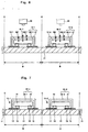
- Figs. 3 to 7 are drawings showing a manufacturing process of the light emitting diode according to the first embodiment.
- like reference numerals are given to like constituent portions to those of the light emitting diode 10 which has been described with reference to Fig. 1.
- a manufacturing method of the light emitting diode 10 according to the first embodiment will be described.
- the manufacturing method will be described by taking as an example a case where two light emitting diodes 10-1 (having an LED element 14-1) and 10-2 (having an LED element 14-2) which have predetermined luminous intensities and wavelengths are manufactured by preparing two LED elements 14-1, 14-2 which differ in luminous intensity and wavelength (tone) and forming a fluorescent material 15-1 (having a thickness M-1) on the LED element 14-1 and a fluorescent material 15-2 (having a thickness M-2) on the LED element 14-2.
- the light emitting diodes 10-1, 10-2 are configured the same as the light emitting diode 10 except that the fluorescent material 22 of the second layer provided on the light emitting diode 10, which is described with reference to Fig. 1, differs in thickness from fluorescent materials 22-1, 22-2 which are provided on the light emitting diodes 10-1, 10-2.
- Figs. 3 to 7 an example is taken in which the light emitting diodes 10-1, 10-2 are manufactured on the substrate 11 having the plurality of light emitting diode forming areas B (refer to Fig. 2) .
- a pair of electrodes 12, 13 are formed on each of a plurality of light emitting diode forming areas B on a substrate 11 made of silicon (in this case, to be specific, a silicon substrate) (an electrode forming step).
- the substrate 11 made of silicon having high thermal conductivity pairs of electrodes 12, 13 to which LED elements 14-1, 14-2 are connected, heat produced and released from the LED elements 14-1, 14-2 can be dissipated with good efficiency.
- a ceramic substrate or a lead frame made of Cu, Ni, Cu alloy or the like may be used as the substrate 11, and in this case, too, a similar advantage to that obtained with the silicon substrate can be obtained.
- the LED elements 14-1, 14-2 are electrically connected to the pairs of electrode pads 12, 13, respectively (an LED element connecting step). Specifically speaking, solder bumps 18 are provided on electrodes 17A, 17B of the LED elements 14-1, 14-2, so that the solder bumps 18 so provided are then connected to the pairs of electrode pads 12, 13.
- a metallic mask 27 having openings 27A through which the LED elements 14-1, 14-2 are exposed is disposed on the substrate 11, and fluorescent materials 21 (having a thickness M1) of first layers are formed by a printing method (a fluorescent material first layer forming step).
- the thickness M1 of the fluorescent materials 21 of the first layers is set to be thinner than thicknesses M-1, M-2 (thicknesses which enable white lights of the light emitting diodes 10-1, 10-2 to have predetermined luminances and wavelengths) of fluorescent materials 15-1, 15-2 but be thicker than thicknesses M2-1, M2-2 of fluorescent materials 22-1, 22-2 of second layers.
- the metallic mask 27 is formed into a shape which covers connecting portions 12A, 13A of the pairs of electrode pads 12, 13, whereby the connecting portions 12A, 13A of the electrode pads 12, 13 can be prevented from being covered by the fluorescent materials 21 of the first layers.
- the metallic mask 27 is removed from the substrate 11 after the fluorescent materials 21 of the first layers has been formed.
- the fluorescent materials 21 of the first layers can be formed substantially simultaneously with respect to the plurality of LED elements 14-1, 14-2 being provided on the substrate 11.
- the fluorescent materials 15-1, 15-2 are formed over the plurality of LED elements 14-1, 14-2 by using only an ink jet method or an evaporation method, formation time of the fluorescent materials 15-1, 15-2 becomes short. Therefore, productivity of the light emitting diodes 10-1, 10-2 can be improved.
- probes (not shown) are brought into contact with the pairs of electrode pads 12, 13, and the LED elements 14-1, 14-2 are caused to emit light sequentially for measurement by a spectral radiometer 26 of luminance and wavelength (tone) on each of the light emitting diodes 10-1, 10-2 in which the fluorescent materials 21 of the first layers have been formed.
- a spectral radiometer 26 for example, a spectral radiometer SR-3 (manufactured by TOPCON TECHNOHOUSE CORPORATION, Ltd.) can be used.
- fluorescent materials 22-1, 22-2 of second layers are sequentially formed by an ink jet method so as to obtain predetermined luminances and wavelengths (a fluorescent material second layer forming step).
- the luminances and wavelengths continue to be measured by the spectral radiometer 26 (a secondary measuring step). Additionally, whether or not the luminances and wavelengths measured during the secondary measuring step have reached the predetermined luminances and wavelengths is determined, and the formation of the fluorescent materials 22-1, 22-2 of the second layers is completed when the luminances and wavelengths measured are determined to have reached the predetermined luminances and wavelengths.
- a structure corresponding to the light emitting diode 10-1 is formed in a light emitting diode forming area B shown in a left-hand side part of Fig. 6, and a structure corresponding to the light emitting diode 10-2 is formed in a light emitting diode forming area shown on a right-hand side part of Fig. 6.
- the light emitting diodes 10-1, 10-2 can be obtained which emit white light of the desired luminance and wavelength (tone), and hence the yield of light emitting diodes 10-1, 10-2 can be increased.
- the fluorescent materials 15-1, 15-2 can be cured without providing separately a curing step.
- the light emitting diodes 10-1, 10-2 are manufactured by cutting the substrate 11 along positions corresponding the cutting positions by means of a dicing blade (not shown).
- the yield of light emitting diodes 10-1, 10-2 can be increased by forming the fluorescent materials 22-1, 22-2 of the second layers so that the light emitting diodes 10-1, 10-2 have the predetermined luminances and wavelengths in such a state that the LED elements 14-1, 14-2 are caused to emit light.
- the fluorescent materials 21 of the first layers and the fluorescent materials 22-1, 22-2 of the second layers may be formed at one time by the ink jet method or vapor deposition method so that the light emitting diodes 10-1, 10-2 can have the predetermined luminances and wavelengths (a fluorescent material forming step) while causing the LED elements 14-1, 14-2 to emit light sequentially for measurement of luminances and wavelengths (tones) (a luminance and wavelength measuring step).
- Fig. 8 is a sectional view of a light emitting diode according to a second embodiment of the invention.
- like reference numerals are given to like constituent portions to those of the light emitting diode 10 of the first embodiment, and the description thereof will be omitted.
- the light emitting diode 30 is configured the same as the light emitting diode 10 of the first embodiment except that in place of the electrode pads 12, 13 provided on the light emitting diode 10 of the first embodiment, electrode pads 31, 32 are provided and furthermore, through vias 33 and external connecting terminals 35 are provided.
- the electrode pads 31, 32 are provided on a substrate 11 in such a manner as to face positions where the through vias 33 are formed.
- the electrode pads 31, 32 are covered by a fluorescent material 21 of a first layer. Either of the electrode pads 31, 32 is a positive electrode pad, and the other of them is a negative electrode pad.
- LED elements 14, 14 are electrically connected to the electrode pads 31, 32 via solder bumps 18.
- the through via 33 is provided in such a manner as to pass through the substrate 11. Either of the electrode pads 31, 32 is provided at one end portion of the through via 33 and the external connecting terminal 35 is provided at the other end portion thereof.
- the through vias 33 establish electrical connections between the electrode pads 31, 32 and the external connecting terminals 35.
- the external connecting terminals 35 are terminals which establish electrical connections to a printed circuit board (not shown). Solder balls, for example, can be used as the external connecting terminals 35.
- the same advantage as that obtained with the light emitting diode 10 of the first embodiment can be obtained.
- this embodiment can be applied to a light emitting diode which includes an LED element which emits a near-ultraviolet ray and fluorescent materials which emit three colors of red, blue and green.
- the light emitting diode 30 of the second embodiment can be manufactured by the same method as that used to manufacture the light emitting diode 10 of the first embodiment except that the electrode pads 31, 32, through vias 33 and external connecting terminals 35 are formed on the substrate 11 by known methods.
- Fig. 9 is a sectional view of a light emitting diode according to a third embodiment of the invention.
- like reference numerals are given to like constituent portions to those of the light emitting diode 10 of the first embodiment, and the description thereof will be omitted.
- the light emitting diode 40 has a substrate 11, a fluorescent material 15, electrode pads 41, 42, an LED element 44 and a wire 45.
- Either of the electrode pads 41, 42 is a positive electrode pad and the other of them is a negative electrode pad.
- the electrode pad 41 is provided on the substrate 11.
- the electrode pad 41 is electrically connected to an electrode 47 of the LED element 44 via the wire 45.
- a wire which is electrically connected to a pad (not shown) on the printed circuit board is connected to the electrode pad 41.
- the electrode pad 42 is provided on the substrate 11.
- the electrode pad 42 has an electrode connecting portion 42A and a connecting portion 42B.
- the electrode connecting portion 42A is covered by the fluorescent material 15 and an electrode 48 of the LED element 44 is connected to the electrode connecting portion 42A.
- the connecting portion 42B is exposed from the fluorescent material 15 and is electrically connected to a pad (not shown) of the printed circuit board via a wire, not shown.
- the LED element 44 is provided on the electrode connecting portion 42A and is covered by the fluorescent material 15.
- the LED element 44 is a device which emits blue light.
- the LED element 44 is configured the same as the LED element 14 described in the first embodiment except that in place of the electrodes 17A, 17B provided on the LED element 14, the electrodes 47, 48 are provided.
- Either of the electrodes 47, 48 is a positive electrode and the other of them is a negative electrode.
- the electrode 47 is provided on an upper surface of the LED element 44.
- the electrode 47 is electrically connected to the electrode pad 41 via the wire 45.
- the electrode 48 is provided on a lower surface of the LED element 44.
- the electrode 48 is electrically connected to the electrode connecting portion 42A via a solder, not shown.
- this embodiment can be applied to a light emitting diode which includes a LED element which emits a near-ultraviolet ray and fluorescent materials which emit three colors of red, blue and green.
- the fluorescent material 15 of the light emitting diode 40 of the third embodiment can be manufactured by the same method as that used to manufacture the fluorescent material 15 of the light emitting diode 10 of the first embodiment.
- the invention can be applied to a light emitting diode which can dissipate heat produced and released from an LED element with good efficiency so as to prevent the failure of the light emitting diode and increase the yield thereof and a manufacturing method thereof.
Landscapes
- Engineering & Computer Science (AREA)
- Microelectronics & Electronic Packaging (AREA)
- Computer Hardware Design (AREA)
- Power Engineering (AREA)
- Manufacturing & Machinery (AREA)
- Led Device Packages (AREA)
Applications Claiming Priority (1)
| Application Number | Priority Date | Filing Date | Title |
|---|---|---|---|
| JP2005254724A JP2007067326A (ja) | 2005-09-02 | 2005-09-02 | 発光ダイオード及びその製造方法 |
Publications (1)
| Publication Number | Publication Date |
|---|---|
| EP1760795A2 true EP1760795A2 (fr) | 2007-03-07 |
Family
ID=37461580
Family Applications (1)
| Application Number | Title | Priority Date | Filing Date |
|---|---|---|---|
| EP06018326A Withdrawn EP1760795A2 (fr) | 2005-09-02 | 2006-09-01 | Diode électroluminescente et son procédé de fabrication |
Country Status (4)
| Country | Link |
|---|---|
| US (2) | US7622317B2 (fr) |
| EP (1) | EP1760795A2 (fr) |
| JP (1) | JP2007067326A (fr) |
| TW (1) | TW200721547A (fr) |
Cited By (37)
| Publication number | Priority date | Publication date | Assignee | Title |
|---|---|---|---|---|
| WO2009008636A2 (fr) | 2007-07-06 | 2009-01-15 | Lg Innotek Co., Ltd | Boîtier de dispositif émettant de la lumière |
| WO2009055079A1 (fr) * | 2007-10-26 | 2009-04-30 | Cree Led Lighting Solutions, Inc. | Dispositif d'éclairage ayant un ou plusieurs luminophores, et procédés pour sa fabrication |
| US7744243B2 (en) | 2007-05-08 | 2010-06-29 | Cree Led Lighting Solutions, Inc. | Lighting device and lighting method |
| US7768192B2 (en) | 2005-12-21 | 2010-08-03 | Cree Led Lighting Solutions, Inc. | Lighting device and lighting method |
| US7791092B2 (en) | 2003-05-01 | 2010-09-07 | Cree, Inc. | Multiple component solid state white light |
| US7821194B2 (en) | 2006-04-18 | 2010-10-26 | Cree, Inc. | Solid state lighting devices including light mixtures |
| US7828460B2 (en) | 2006-04-18 | 2010-11-09 | Cree, Inc. | Lighting device and lighting method |
| US7863635B2 (en) | 2007-08-07 | 2011-01-04 | Cree, Inc. | Semiconductor light emitting devices with applied wavelength conversion materials |
| US7901107B2 (en) | 2007-05-08 | 2011-03-08 | Cree, Inc. | Lighting device and lighting method |
| US7918581B2 (en) | 2006-12-07 | 2011-04-05 | Cree, Inc. | Lighting device and lighting method |
| US7997745B2 (en) | 2006-04-20 | 2011-08-16 | Cree, Inc. | Lighting device and lighting method |
| US8018135B2 (en) | 2007-10-10 | 2011-09-13 | Cree, Inc. | Lighting device and method of making |
| US8029155B2 (en) | 2006-11-07 | 2011-10-04 | Cree, Inc. | Lighting device and lighting method |
| US8038317B2 (en) | 2007-05-08 | 2011-10-18 | Cree, Inc. | Lighting device and lighting method |
| US8079729B2 (en) | 2007-05-08 | 2011-12-20 | Cree, Inc. | Lighting device and lighting method |
| US8120240B2 (en) | 2005-01-10 | 2012-02-21 | Cree, Inc. | Light emission device and method utilizing multiple emitters |
| US8125137B2 (en) | 2005-01-10 | 2012-02-28 | Cree, Inc. | Multi-chip light emitting device lamps for providing high-CRI warm white light and light fixtures including the same |
| US8328376B2 (en) | 2005-12-22 | 2012-12-11 | Cree, Inc. | Lighting device |
| US8337071B2 (en) | 2005-12-21 | 2012-12-25 | Cree, Inc. | Lighting device |
| US8350461B2 (en) | 2008-03-28 | 2013-01-08 | Cree, Inc. | Apparatus and methods for combining light emitters |
| US8506114B2 (en) | 2007-02-22 | 2013-08-13 | Cree, Inc. | Lighting devices, methods of lighting, light filters and methods of filtering light |
| US8513875B2 (en) | 2006-04-18 | 2013-08-20 | Cree, Inc. | Lighting device and lighting method |
| US8556469B2 (en) | 2010-12-06 | 2013-10-15 | Cree, Inc. | High efficiency total internal reflection optic for solid state lighting luminaires |
| US8596819B2 (en) | 2006-05-31 | 2013-12-03 | Cree, Inc. | Lighting device and method of lighting |
| US8684559B2 (en) | 2010-06-04 | 2014-04-01 | Cree, Inc. | Solid state light source emitting warm light with high CRI |
| EP2725630A1 (fr) * | 2012-10-29 | 2014-04-30 | LG Innotek Co., Ltd. | Dispositif électroluminescent |
| US8921876B2 (en) | 2009-06-02 | 2014-12-30 | Cree, Inc. | Lighting devices with discrete lumiphor-bearing regions within or on a surface of remote elements |
| US8967821B2 (en) | 2009-09-25 | 2015-03-03 | Cree, Inc. | Lighting device with low glare and high light level uniformity |
| EP2541631A4 (fr) * | 2010-02-25 | 2015-03-18 | Lightizer Korea Co Ltd | Diode émettrice de lumière et procédé de fabrication |
| US9084328B2 (en) | 2006-12-01 | 2015-07-14 | Cree, Inc. | Lighting device and lighting method |
| US9217553B2 (en) | 2007-02-21 | 2015-12-22 | Cree, Inc. | LED lighting systems including luminescent layers on remote reflectors |
| US9275979B2 (en) | 2010-03-03 | 2016-03-01 | Cree, Inc. | Enhanced color rendering index emitter through phosphor separation |
| US9435493B2 (en) | 2009-10-27 | 2016-09-06 | Cree, Inc. | Hybrid reflector system for lighting device |
| US9441793B2 (en) | 2006-12-01 | 2016-09-13 | Cree, Inc. | High efficiency lighting device including one or more solid state light emitters, and method of lighting |
| US10030824B2 (en) | 2007-05-08 | 2018-07-24 | Cree, Inc. | Lighting device and lighting method |
| US10615324B2 (en) | 2013-06-14 | 2020-04-07 | Cree Huizhou Solid State Lighting Company Limited | Tiny 6 pin side view surface mount LED |
| US11251164B2 (en) | 2011-02-16 | 2022-02-15 | Creeled, Inc. | Multi-layer conversion material for down conversion in solid state lighting |
Families Citing this family (18)
| Publication number | Priority date | Publication date | Assignee | Title |
|---|---|---|---|---|
| US8999736B2 (en) | 2003-07-04 | 2015-04-07 | Epistar Corporation | Optoelectronic system |
| US8998444B2 (en) * | 2006-04-18 | 2015-04-07 | Cree, Inc. | Solid state lighting devices including light mixtures |
| CN101431934B (zh) * | 2006-04-26 | 2011-01-05 | 皇家飞利浦电子股份有限公司 | 具有改进的转换元件的光传输装置 |
| WO2008045927A2 (fr) * | 2006-10-12 | 2008-04-17 | Cree Led Lighting Solutions, Inc. | Dispositif d'éclairage et son procédé de fabrication |
| CN101266180A (zh) * | 2007-03-16 | 2008-09-17 | 清华大学 | 电离规 |
| JP4926789B2 (ja) * | 2007-03-31 | 2012-05-09 | 株式会社住友金属エレクトロデバイス | 発光素子実装用多層配線基板とその製造方法 |
| JP5137059B2 (ja) * | 2007-06-20 | 2013-02-06 | 新光電気工業株式会社 | 電子部品用パッケージ及びその製造方法と電子部品装置 |
| US20090039375A1 (en) * | 2007-08-07 | 2009-02-12 | Cree, Inc. | Semiconductor light emitting devices with separated wavelength conversion materials and methods of forming the same |
| US8240875B2 (en) * | 2008-06-25 | 2012-08-14 | Cree, Inc. | Solid state linear array modules for general illumination |
| GB2462411B (en) * | 2008-07-30 | 2013-05-22 | Photonstar Led Ltd | Tunable colour led module |
| US20100105156A1 (en) * | 2008-10-27 | 2010-04-29 | Po-Shen Chen | Method of manufacturing light-emitting diode package |
| US7967652B2 (en) | 2009-02-19 | 2011-06-28 | Cree, Inc. | Methods for combining light emitting devices in a package and packages including combined light emitting devices |
| US8333631B2 (en) * | 2009-02-19 | 2012-12-18 | Cree, Inc. | Methods for combining light emitting devices in a package and packages including combined light emitting devices |
| CN102420282B (zh) * | 2010-09-27 | 2014-07-02 | 展晶科技(深圳)有限公司 | 发光二极管封装结构及其制造方法 |
| JP5985846B2 (ja) * | 2011-06-29 | 2016-09-06 | Flexceed株式会社 | 発光素子搭載用基板及びledパッケージ |
| KR20170096258A (ko) * | 2016-02-15 | 2017-08-24 | 삼성전자주식회사 | 검사장치 |
| TWI775888B (zh) * | 2018-02-14 | 2022-09-01 | 晶元光電股份有限公司 | 發光裝置、其製造方法及顯示模組 |
| KR20190098709A (ko) * | 2018-02-14 | 2019-08-22 | 에피스타 코포레이션 | 발광 장치, 그 제조 방법 및 디스플레이 모듈 |
Family Cites Families (7)
| Publication number | Priority date | Publication date | Assignee | Title |
|---|---|---|---|---|
| TW383508B (en) * | 1996-07-29 | 2000-03-01 | Nichia Kagaku Kogyo Kk | Light emitting device and display |
| JP3546650B2 (ja) * | 1997-07-28 | 2004-07-28 | 日亜化学工業株式会社 | 発光ダイオードの形成方法 |
| JP2000223749A (ja) | 1999-01-29 | 2000-08-11 | Seiwa Electric Mfg Co Ltd | 発光ダイオードランプとその製造方法、チップ型発光ダイオード素子及びドットマトリクス型発光ダイオードユニット |
| JP3399440B2 (ja) * | 1999-04-26 | 2003-04-21 | 松下電器産業株式会社 | 複合発光素子と発光装置及びその製造方法 |
| JP4114331B2 (ja) * | 2001-06-15 | 2008-07-09 | 豊田合成株式会社 | 発光装置 |
| US7858403B2 (en) * | 2001-10-31 | 2010-12-28 | Cree, Inc. | Methods and systems for fabricating broad spectrum light emitting devices |
| TWI239670B (en) * | 2004-12-29 | 2005-09-11 | Ind Tech Res Inst | Package structure of light emitting diode and its manufacture method |
-
2005
- 2005-09-02 JP JP2005254724A patent/JP2007067326A/ja active Pending
-
2006
- 2006-08-31 US US11/469,026 patent/US7622317B2/en not_active Expired - Fee Related
- 2006-09-01 EP EP06018326A patent/EP1760795A2/fr not_active Withdrawn
- 2006-09-01 TW TW095132341A patent/TW200721547A/zh unknown
-
2009
- 2009-09-16 US US12/560,934 patent/US20100001304A1/en not_active Abandoned
Cited By (59)
| Publication number | Priority date | Publication date | Assignee | Title |
|---|---|---|---|---|
| US8901585B2 (en) | 2003-05-01 | 2014-12-02 | Cree, Inc. | Multiple component solid state white light |
| US7791092B2 (en) | 2003-05-01 | 2010-09-07 | Cree, Inc. | Multiple component solid state white light |
| US8513873B2 (en) | 2005-01-10 | 2013-08-20 | Cree, Inc. | Light emission device |
| US8410680B2 (en) | 2005-01-10 | 2013-04-02 | Cree, Inc. | Multi-chip light emitting device lamps for providing high-CRI warm white light and light fixtures including the same |
| US8125137B2 (en) | 2005-01-10 | 2012-02-28 | Cree, Inc. | Multi-chip light emitting device lamps for providing high-CRI warm white light and light fixtures including the same |
| US8120240B2 (en) | 2005-01-10 | 2012-02-21 | Cree, Inc. | Light emission device and method utilizing multiple emitters |
| US8337071B2 (en) | 2005-12-21 | 2012-12-25 | Cree, Inc. | Lighting device |
| US7768192B2 (en) | 2005-12-21 | 2010-08-03 | Cree Led Lighting Solutions, Inc. | Lighting device and lighting method |
| US8878429B2 (en) | 2005-12-21 | 2014-11-04 | Cree, Inc. | Lighting device and lighting method |
| US8328376B2 (en) | 2005-12-22 | 2012-12-11 | Cree, Inc. | Lighting device |
| US8858004B2 (en) | 2005-12-22 | 2014-10-14 | Cree, Inc. | Lighting device |
| US7828460B2 (en) | 2006-04-18 | 2010-11-09 | Cree, Inc. | Lighting device and lighting method |
| US8733968B2 (en) | 2006-04-18 | 2014-05-27 | Cree, Inc. | Lighting device and lighting method |
| US10018346B2 (en) | 2006-04-18 | 2018-07-10 | Cree, Inc. | Lighting device and lighting method |
| US8513875B2 (en) | 2006-04-18 | 2013-08-20 | Cree, Inc. | Lighting device and lighting method |
| US9297503B2 (en) | 2006-04-18 | 2016-03-29 | Cree, Inc. | Lighting device and lighting method |
| US8123376B2 (en) | 2006-04-18 | 2012-02-28 | Cree, Inc. | Lighting device and lighting method |
| US8212466B2 (en) | 2006-04-18 | 2012-07-03 | Cree, Inc. | Solid state lighting devices including light mixtures |
| US7821194B2 (en) | 2006-04-18 | 2010-10-26 | Cree, Inc. | Solid state lighting devices including light mixtures |
| US9417478B2 (en) | 2006-04-18 | 2016-08-16 | Cree, Inc. | Lighting device and lighting method |
| US7997745B2 (en) | 2006-04-20 | 2011-08-16 | Cree, Inc. | Lighting device and lighting method |
| US8628214B2 (en) | 2006-05-31 | 2014-01-14 | Cree, Inc. | Lighting device and lighting method |
| US8596819B2 (en) | 2006-05-31 | 2013-12-03 | Cree, Inc. | Lighting device and method of lighting |
| US8382318B2 (en) | 2006-11-07 | 2013-02-26 | Cree, Inc. | Lighting device and lighting method |
| US8029155B2 (en) | 2006-11-07 | 2011-10-04 | Cree, Inc. | Lighting device and lighting method |
| US9441793B2 (en) | 2006-12-01 | 2016-09-13 | Cree, Inc. | High efficiency lighting device including one or more solid state light emitters, and method of lighting |
| US9084328B2 (en) | 2006-12-01 | 2015-07-14 | Cree, Inc. | Lighting device and lighting method |
| US7918581B2 (en) | 2006-12-07 | 2011-04-05 | Cree, Inc. | Lighting device and lighting method |
| US9217553B2 (en) | 2007-02-21 | 2015-12-22 | Cree, Inc. | LED lighting systems including luminescent layers on remote reflectors |
| US8506114B2 (en) | 2007-02-22 | 2013-08-13 | Cree, Inc. | Lighting devices, methods of lighting, light filters and methods of filtering light |
| US8038317B2 (en) | 2007-05-08 | 2011-10-18 | Cree, Inc. | Lighting device and lighting method |
| US8079729B2 (en) | 2007-05-08 | 2011-12-20 | Cree, Inc. | Lighting device and lighting method |
| US10030824B2 (en) | 2007-05-08 | 2018-07-24 | Cree, Inc. | Lighting device and lighting method |
| US7744243B2 (en) | 2007-05-08 | 2010-06-29 | Cree Led Lighting Solutions, Inc. | Lighting device and lighting method |
| US7901107B2 (en) | 2007-05-08 | 2011-03-08 | Cree, Inc. | Lighting device and lighting method |
| EP2171773A4 (fr) * | 2007-07-06 | 2011-03-09 | Lg Innotek Co Ltd | Boîtier de dispositif émettant de la lumière |
| US9368697B2 (en) | 2007-07-06 | 2016-06-14 | Lg Innotek Co., Ltd. | Light emitting device package |
| US8610255B2 (en) | 2007-07-06 | 2013-12-17 | Lg Innotek Co., Ltd. | Light emitting device package |
| WO2009008636A2 (fr) | 2007-07-06 | 2009-01-15 | Lg Innotek Co., Ltd | Boîtier de dispositif émettant de la lumière |
| US8890297B2 (en) | 2007-07-06 | 2014-11-18 | Lg Innotek Co., Ltd. | Light emitting device package |
| EP2171773A2 (fr) * | 2007-07-06 | 2010-04-07 | LG Innotek Co., Ltd. | Boîtier de dispositif émettant de la lumière |
| US7863635B2 (en) | 2007-08-07 | 2011-01-04 | Cree, Inc. | Semiconductor light emitting devices with applied wavelength conversion materials |
| US9054282B2 (en) | 2007-08-07 | 2015-06-09 | Cree, Inc. | Semiconductor light emitting devices with applied wavelength conversion materials and methods for forming the same |
| US8018135B2 (en) | 2007-10-10 | 2011-09-13 | Cree, Inc. | Lighting device and method of making |
| WO2009055079A1 (fr) * | 2007-10-26 | 2009-04-30 | Cree Led Lighting Solutions, Inc. | Dispositif d'éclairage ayant un ou plusieurs luminophores, et procédés pour sa fabrication |
| US8350461B2 (en) | 2008-03-28 | 2013-01-08 | Cree, Inc. | Apparatus and methods for combining light emitters |
| US8513871B2 (en) | 2008-03-28 | 2013-08-20 | Cree, Inc. | Apparatus and methods for combining light emitters |
| US8921876B2 (en) | 2009-06-02 | 2014-12-30 | Cree, Inc. | Lighting devices with discrete lumiphor-bearing regions within or on a surface of remote elements |
| US8967821B2 (en) | 2009-09-25 | 2015-03-03 | Cree, Inc. | Lighting device with low glare and high light level uniformity |
| US9435493B2 (en) | 2009-10-27 | 2016-09-06 | Cree, Inc. | Hybrid reflector system for lighting device |
| EP2541631A4 (fr) * | 2010-02-25 | 2015-03-18 | Lightizer Korea Co Ltd | Diode émettrice de lumière et procédé de fabrication |
| US9275979B2 (en) | 2010-03-03 | 2016-03-01 | Cree, Inc. | Enhanced color rendering index emitter through phosphor separation |
| US8684559B2 (en) | 2010-06-04 | 2014-04-01 | Cree, Inc. | Solid state light source emitting warm light with high CRI |
| US9599291B2 (en) | 2010-06-04 | 2017-03-21 | Cree, Inc. | Solid state light source emitting warm light with high CRI |
| US8556469B2 (en) | 2010-12-06 | 2013-10-15 | Cree, Inc. | High efficiency total internal reflection optic for solid state lighting luminaires |
| US11251164B2 (en) | 2011-02-16 | 2022-02-15 | Creeled, Inc. | Multi-layer conversion material for down conversion in solid state lighting |
| US9437784B2 (en) | 2012-10-29 | 2016-09-06 | Lg Innotek Co., Ltd. | Light emitting device |
| EP2725630A1 (fr) * | 2012-10-29 | 2014-04-30 | LG Innotek Co., Ltd. | Dispositif électroluminescent |
| US10615324B2 (en) | 2013-06-14 | 2020-04-07 | Cree Huizhou Solid State Lighting Company Limited | Tiny 6 pin side view surface mount LED |
Also Published As
| Publication number | Publication date |
|---|---|
| US20070051966A1 (en) | 2007-03-08 |
| TW200721547A (en) | 2007-06-01 |
| US20100001304A1 (en) | 2010-01-07 |
| US7622317B2 (en) | 2009-11-24 |
| JP2007067326A (ja) | 2007-03-15 |
Similar Documents
| Publication | Publication Date | Title |
|---|---|---|
| US7622317B2 (en) | Light emitting diode and method for manufacturing the same | |
| US8378377B2 (en) | Light emitting device | |
| US8403536B2 (en) | Light-emitting module and illuminating apparatus having an insulating base having a plurality of insulating layers | |
| US7755095B2 (en) | Semiconductor light emitting device, lighting module, lighting apparatus, display element, and manufacturing method for semiconductor light emitting device | |
| US8410502B2 (en) | Light-emitting device, planar light source including the light-emitting device, and liquid crystal display device including the planar light source | |
| US8207548B2 (en) | Semiconductor light emitting device, light emitting module, lighting apparatus, display element and manufacturing method of semiconductor light emitting device | |
| EP2299503A2 (fr) | Boîtier de composant luminescent et son procédé de fabrication | |
| JP5398644B2 (ja) | 半導体発光装置を用いた光源装置 | |
| JPWO2005106978A1 (ja) | 発光装置およびその製造方法 | |
| JP2004253404A (ja) | 発光素子収納用パッケージおよび発光装置 | |
| KR20110000730A (ko) | 표면 실장 led 모듈 및 표면 실장 led 모듈의 제조 방법 | |
| JP4193905B2 (ja) | 半導体装置の製造方法 | |
| KR20190129178A (ko) | 박막 패드를 구비하는 발광 소자 패키지 및 그 제조 방법 | |
| KR20130062985A (ko) | 복사 방출 소자 및 복사 방출 소자의 제조 방법 | |
| JP2004253711A (ja) | 発光素子収納用パッケージおよび発光装置 | |
| JP2004311456A (ja) | 発光素子収納用パッケージおよび発光装置 | |
| JP2004047617A (ja) | 電子部品の実装構造及びその製造方法 | |
| WO2016174892A1 (fr) | Boîtier de del, dispositif d'émission de lumière et procédé de fabrication du boîtier de del | |
| JP2006059851A (ja) | 半導体発光装置、それを用いた照明装置およびその製造方法 | |
| US10522730B2 (en) | LED lighting apparatus | |
| JP6269356B2 (ja) | 発光装置 | |
| JP5592963B2 (ja) | 半導体発光装置を用いた光源装置 | |
| JP7260309B2 (ja) | 半導体発光装置 | |
| US20220069184A1 (en) | Semiconductor light emitting device and method for manufacturing the same |
Legal Events
| Date | Code | Title | Description |
|---|---|---|---|
| PUAI | Public reference made under article 153(3) epc to a published international application that has entered the european phase |
Free format text: ORIGINAL CODE: 0009012 |
|
| AK | Designated contracting states |
Kind code of ref document: A2 Designated state(s): AT BE BG CH CY CZ DE DK EE ES FI FR GB GR HU IE IS IT LI LT LU LV MC NL PL PT RO SE SI SK TR |
|
| AX | Request for extension of the european patent |
Extension state: AL BA HR MK YU |
|
| STAA | Information on the status of an ep patent application or granted ep patent |
Free format text: STATUS: THE APPLICATION HAS BEEN WITHDRAWN |
|
| 18W | Application withdrawn |
Effective date: 20111017 |