EP1758086A2 - Data driving circuit and driving method of organic light emitting display using the same - Google Patents
Data driving circuit and driving method of organic light emitting display using the same Download PDFInfo
- Publication number
- EP1758086A2 EP1758086A2 EP06254047A EP06254047A EP1758086A2 EP 1758086 A2 EP1758086 A2 EP 1758086A2 EP 06254047 A EP06254047 A EP 06254047A EP 06254047 A EP06254047 A EP 06254047A EP 1758086 A2 EP1758086 A2 EP 1758086A2
- Authority
- EP
- European Patent Office
- Prior art keywords
- data
- voltage
- transistor
- pixel
- period
- Prior art date
- Legal status (The legal status is an assumption and is not a legal conclusion. Google has not performed a legal analysis and makes no representation as to the accuracy of the status listed.)
- Granted
Links
Images





Classifications
-
- G—PHYSICS
- G09—EDUCATION; CRYPTOGRAPHY; DISPLAY; ADVERTISING; SEALS
- G09G—ARRANGEMENTS OR CIRCUITS FOR CONTROL OF INDICATING DEVICES USING STATIC MEANS TO PRESENT VARIABLE INFORMATION
- G09G3/00—Control arrangements or circuits, of interest only in connection with visual indicators other than cathode-ray tubes
- G09G3/20—Control arrangements or circuits, of interest only in connection with visual indicators other than cathode-ray tubes for presentation of an assembly of a number of characters, e.g. a page, by composing the assembly by combination of individual elements arranged in a matrix no fixed position being assigned to or needed to be assigned to the individual characters or partial characters
- G09G3/22—Control arrangements or circuits, of interest only in connection with visual indicators other than cathode-ray tubes for presentation of an assembly of a number of characters, e.g. a page, by composing the assembly by combination of individual elements arranged in a matrix no fixed position being assigned to or needed to be assigned to the individual characters or partial characters using controlled light sources
- G09G3/30—Control arrangements or circuits, of interest only in connection with visual indicators other than cathode-ray tubes for presentation of an assembly of a number of characters, e.g. a page, by composing the assembly by combination of individual elements arranged in a matrix no fixed position being assigned to or needed to be assigned to the individual characters or partial characters using controlled light sources using electroluminescent panels
- G09G3/32—Control arrangements or circuits, of interest only in connection with visual indicators other than cathode-ray tubes for presentation of an assembly of a number of characters, e.g. a page, by composing the assembly by combination of individual elements arranged in a matrix no fixed position being assigned to or needed to be assigned to the individual characters or partial characters using controlled light sources using electroluminescent panels semiconductive, e.g. using light-emitting diodes [LED]
- G09G3/3208—Control arrangements or circuits, of interest only in connection with visual indicators other than cathode-ray tubes for presentation of an assembly of a number of characters, e.g. a page, by composing the assembly by combination of individual elements arranged in a matrix no fixed position being assigned to or needed to be assigned to the individual characters or partial characters using controlled light sources using electroluminescent panels semiconductive, e.g. using light-emitting diodes [LED] organic, e.g. using organic light-emitting diodes [OLED]
- G09G3/3225—Control arrangements or circuits, of interest only in connection with visual indicators other than cathode-ray tubes for presentation of an assembly of a number of characters, e.g. a page, by composing the assembly by combination of individual elements arranged in a matrix no fixed position being assigned to or needed to be assigned to the individual characters or partial characters using controlled light sources using electroluminescent panels semiconductive, e.g. using light-emitting diodes [LED] organic, e.g. using organic light-emitting diodes [OLED] using an active matrix
- G09G3/3233—Control arrangements or circuits, of interest only in connection with visual indicators other than cathode-ray tubes for presentation of an assembly of a number of characters, e.g. a page, by composing the assembly by combination of individual elements arranged in a matrix no fixed position being assigned to or needed to be assigned to the individual characters or partial characters using controlled light sources using electroluminescent panels semiconductive, e.g. using light-emitting diodes [LED] organic, e.g. using organic light-emitting diodes [OLED] using an active matrix with pixel circuitry controlling the current through the light-emitting element
-
- G—PHYSICS
- G09—EDUCATION; CRYPTOGRAPHY; DISPLAY; ADVERTISING; SEALS
- G09G—ARRANGEMENTS OR CIRCUITS FOR CONTROL OF INDICATING DEVICES USING STATIC MEANS TO PRESENT VARIABLE INFORMATION
- G09G3/00—Control arrangements or circuits, of interest only in connection with visual indicators other than cathode-ray tubes
- G09G3/20—Control arrangements or circuits, of interest only in connection with visual indicators other than cathode-ray tubes for presentation of an assembly of a number of characters, e.g. a page, by composing the assembly by combination of individual elements arranged in a matrix no fixed position being assigned to or needed to be assigned to the individual characters or partial characters
- G09G3/22—Control arrangements or circuits, of interest only in connection with visual indicators other than cathode-ray tubes for presentation of an assembly of a number of characters, e.g. a page, by composing the assembly by combination of individual elements arranged in a matrix no fixed position being assigned to or needed to be assigned to the individual characters or partial characters using controlled light sources
- G09G3/30—Control arrangements or circuits, of interest only in connection with visual indicators other than cathode-ray tubes for presentation of an assembly of a number of characters, e.g. a page, by composing the assembly by combination of individual elements arranged in a matrix no fixed position being assigned to or needed to be assigned to the individual characters or partial characters using controlled light sources using electroluminescent panels
-
- G—PHYSICS
- G09—EDUCATION; CRYPTOGRAPHY; DISPLAY; ADVERTISING; SEALS
- G09G—ARRANGEMENTS OR CIRCUITS FOR CONTROL OF INDICATING DEVICES USING STATIC MEANS TO PRESENT VARIABLE INFORMATION
- G09G3/00—Control arrangements or circuits, of interest only in connection with visual indicators other than cathode-ray tubes
- G09G3/20—Control arrangements or circuits, of interest only in connection with visual indicators other than cathode-ray tubes for presentation of an assembly of a number of characters, e.g. a page, by composing the assembly by combination of individual elements arranged in a matrix no fixed position being assigned to or needed to be assigned to the individual characters or partial characters
- G09G3/2007—Display of intermediate tones
- G09G3/2011—Display of intermediate tones by amplitude modulation
-
- G—PHYSICS
- G09—EDUCATION; CRYPTOGRAPHY; DISPLAY; ADVERTISING; SEALS
- G09G—ARRANGEMENTS OR CIRCUITS FOR CONTROL OF INDICATING DEVICES USING STATIC MEANS TO PRESENT VARIABLE INFORMATION
- G09G3/00—Control arrangements or circuits, of interest only in connection with visual indicators other than cathode-ray tubes
- G09G3/20—Control arrangements or circuits, of interest only in connection with visual indicators other than cathode-ray tubes for presentation of an assembly of a number of characters, e.g. a page, by composing the assembly by combination of individual elements arranged in a matrix no fixed position being assigned to or needed to be assigned to the individual characters or partial characters
- G09G3/22—Control arrangements or circuits, of interest only in connection with visual indicators other than cathode-ray tubes for presentation of an assembly of a number of characters, e.g. a page, by composing the assembly by combination of individual elements arranged in a matrix no fixed position being assigned to or needed to be assigned to the individual characters or partial characters using controlled light sources
- G09G3/30—Control arrangements or circuits, of interest only in connection with visual indicators other than cathode-ray tubes for presentation of an assembly of a number of characters, e.g. a page, by composing the assembly by combination of individual elements arranged in a matrix no fixed position being assigned to or needed to be assigned to the individual characters or partial characters using controlled light sources using electroluminescent panels
- G09G3/32—Control arrangements or circuits, of interest only in connection with visual indicators other than cathode-ray tubes for presentation of an assembly of a number of characters, e.g. a page, by composing the assembly by combination of individual elements arranged in a matrix no fixed position being assigned to or needed to be assigned to the individual characters or partial characters using controlled light sources using electroluminescent panels semiconductive, e.g. using light-emitting diodes [LED]
- G09G3/3208—Control arrangements or circuits, of interest only in connection with visual indicators other than cathode-ray tubes for presentation of an assembly of a number of characters, e.g. a page, by composing the assembly by combination of individual elements arranged in a matrix no fixed position being assigned to or needed to be assigned to the individual characters or partial characters using controlled light sources using electroluminescent panels semiconductive, e.g. using light-emitting diodes [LED] organic, e.g. using organic light-emitting diodes [OLED]
- G09G3/3275—Details of drivers for data electrodes
- G09G3/3283—Details of drivers for data electrodes in which the data driver supplies a variable data current for setting the current through, or the voltage across, the light-emitting elements
-
- G—PHYSICS
- G09—EDUCATION; CRYPTOGRAPHY; DISPLAY; ADVERTISING; SEALS
- G09G—ARRANGEMENTS OR CIRCUITS FOR CONTROL OF INDICATING DEVICES USING STATIC MEANS TO PRESENT VARIABLE INFORMATION
- G09G3/00—Control arrangements or circuits, of interest only in connection with visual indicators other than cathode-ray tubes
- G09G3/20—Control arrangements or circuits, of interest only in connection with visual indicators other than cathode-ray tubes for presentation of an assembly of a number of characters, e.g. a page, by composing the assembly by combination of individual elements arranged in a matrix no fixed position being assigned to or needed to be assigned to the individual characters or partial characters
- G09G3/22—Control arrangements or circuits, of interest only in connection with visual indicators other than cathode-ray tubes for presentation of an assembly of a number of characters, e.g. a page, by composing the assembly by combination of individual elements arranged in a matrix no fixed position being assigned to or needed to be assigned to the individual characters or partial characters using controlled light sources
- G09G3/30—Control arrangements or circuits, of interest only in connection with visual indicators other than cathode-ray tubes for presentation of an assembly of a number of characters, e.g. a page, by composing the assembly by combination of individual elements arranged in a matrix no fixed position being assigned to or needed to be assigned to the individual characters or partial characters using controlled light sources using electroluminescent panels
- G09G3/32—Control arrangements or circuits, of interest only in connection with visual indicators other than cathode-ray tubes for presentation of an assembly of a number of characters, e.g. a page, by composing the assembly by combination of individual elements arranged in a matrix no fixed position being assigned to or needed to be assigned to the individual characters or partial characters using controlled light sources using electroluminescent panels semiconductive, e.g. using light-emitting diodes [LED]
- G09G3/3208—Control arrangements or circuits, of interest only in connection with visual indicators other than cathode-ray tubes for presentation of an assembly of a number of characters, e.g. a page, by composing the assembly by combination of individual elements arranged in a matrix no fixed position being assigned to or needed to be assigned to the individual characters or partial characters using controlled light sources using electroluminescent panels semiconductive, e.g. using light-emitting diodes [LED] organic, e.g. using organic light-emitting diodes [OLED]
- G09G3/3275—Details of drivers for data electrodes
- G09G3/3291—Details of drivers for data electrodes in which the data driver supplies a variable data voltage for setting the current through, or the voltage across, the light-emitting elements
-
- G—PHYSICS
- G09—EDUCATION; CRYPTOGRAPHY; DISPLAY; ADVERTISING; SEALS
- G09G—ARRANGEMENTS OR CIRCUITS FOR CONTROL OF INDICATING DEVICES USING STATIC MEANS TO PRESENT VARIABLE INFORMATION
- G09G2300/00—Aspects of the constitution of display devices
- G09G2300/08—Active matrix structure, i.e. with use of active elements, inclusive of non-linear two terminal elements, in the pixels together with light emitting or modulating elements
- G09G2300/0809—Several active elements per pixel in active matrix panels
- G09G2300/0819—Several active elements per pixel in active matrix panels used for counteracting undesired variations, e.g. feedback or autozeroing
-
- G—PHYSICS
- G09—EDUCATION; CRYPTOGRAPHY; DISPLAY; ADVERTISING; SEALS
- G09G—ARRANGEMENTS OR CIRCUITS FOR CONTROL OF INDICATING DEVICES USING STATIC MEANS TO PRESENT VARIABLE INFORMATION
- G09G2300/00—Aspects of the constitution of display devices
- G09G2300/08—Active matrix structure, i.e. with use of active elements, inclusive of non-linear two terminal elements, in the pixels together with light emitting or modulating elements
- G09G2300/0809—Several active elements per pixel in active matrix panels
- G09G2300/0842—Several active elements per pixel in active matrix panels forming a memory circuit, e.g. a dynamic memory with one capacitor
- G09G2300/0852—Several active elements per pixel in active matrix panels forming a memory circuit, e.g. a dynamic memory with one capacitor being a dynamic memory with more than one capacitor
-
- G—PHYSICS
- G09—EDUCATION; CRYPTOGRAPHY; DISPLAY; ADVERTISING; SEALS
- G09G—ARRANGEMENTS OR CIRCUITS FOR CONTROL OF INDICATING DEVICES USING STATIC MEANS TO PRESENT VARIABLE INFORMATION
- G09G2300/00—Aspects of the constitution of display devices
- G09G2300/08—Active matrix structure, i.e. with use of active elements, inclusive of non-linear two terminal elements, in the pixels together with light emitting or modulating elements
- G09G2300/0809—Several active elements per pixel in active matrix panels
- G09G2300/0842—Several active elements per pixel in active matrix panels forming a memory circuit, e.g. a dynamic memory with one capacitor
- G09G2300/0861—Several active elements per pixel in active matrix panels forming a memory circuit, e.g. a dynamic memory with one capacitor with additional control of the display period without amending the charge stored in a pixel memory, e.g. by means of additional select electrodes
-
- G—PHYSICS
- G09—EDUCATION; CRYPTOGRAPHY; DISPLAY; ADVERTISING; SEALS
- G09G—ARRANGEMENTS OR CIRCUITS FOR CONTROL OF INDICATING DEVICES USING STATIC MEANS TO PRESENT VARIABLE INFORMATION
- G09G2310/00—Command of the display device
- G09G2310/02—Addressing, scanning or driving the display screen or processing steps related thereto
- G09G2310/0243—Details of the generation of driving signals
- G09G2310/0251—Precharge or discharge of pixel before applying new pixel voltage
-
- G—PHYSICS
- G09—EDUCATION; CRYPTOGRAPHY; DISPLAY; ADVERTISING; SEALS
- G09G—ARRANGEMENTS OR CIRCUITS FOR CONTROL OF INDICATING DEVICES USING STATIC MEANS TO PRESENT VARIABLE INFORMATION
- G09G2310/00—Command of the display device
- G09G2310/02—Addressing, scanning or driving the display screen or processing steps related thereto
- G09G2310/0264—Details of driving circuits
- G09G2310/027—Details of drivers for data electrodes, the drivers handling digital grey scale data, e.g. use of D/A converters
-
- G—PHYSICS
- G09—EDUCATION; CRYPTOGRAPHY; DISPLAY; ADVERTISING; SEALS
- G09G—ARRANGEMENTS OR CIRCUITS FOR CONTROL OF INDICATING DEVICES USING STATIC MEANS TO PRESENT VARIABLE INFORMATION
- G09G2310/00—Command of the display device
- G09G2310/02—Addressing, scanning or driving the display screen or processing steps related thereto
- G09G2310/0264—Details of driving circuits
- G09G2310/0289—Details of voltage level shifters arranged for use in a driving circuit
-
- G—PHYSICS
- G09—EDUCATION; CRYPTOGRAPHY; DISPLAY; ADVERTISING; SEALS
- G09G—ARRANGEMENTS OR CIRCUITS FOR CONTROL OF INDICATING DEVICES USING STATIC MEANS TO PRESENT VARIABLE INFORMATION
- G09G2320/00—Control of display operating conditions
- G09G2320/02—Improving the quality of display appearance
- G09G2320/0271—Adjustment of the gradation levels within the range of the gradation scale, e.g. by redistribution or clipping
- G09G2320/0276—Adjustment of the gradation levels within the range of the gradation scale, e.g. by redistribution or clipping for the purpose of adaptation to the characteristics of a display device, i.e. gamma correction
-
- G—PHYSICS
- G09—EDUCATION; CRYPTOGRAPHY; DISPLAY; ADVERTISING; SEALS
- G09G—ARRANGEMENTS OR CIRCUITS FOR CONTROL OF INDICATING DEVICES USING STATIC MEANS TO PRESENT VARIABLE INFORMATION
- G09G2320/00—Control of display operating conditions
- G09G2320/04—Maintaining the quality of display appearance
- G09G2320/043—Preventing or counteracting the effects of ageing
Definitions
- the present invention relates to data driving circuits, light emitting displays employing such data driving circuits and methods of driving the light emitting display. More particularly, the invention relates to a data driving circuit capable of displaying images with uniform brightness, a light emitting display using such a data driving circuit and a method of driving the light emitting display to display images with uniform brightness.
- FPDs Flat panel displays
- CRTs cathode ray tubes
- FPDs include liquid crystal displays (LCDs), field emission displays (FEDs), plasma display panels (PDPs) and light emitting displays.
- LCDs liquid crystal displays
- FEDs field emission displays
- PDPs plasma display panels
- Light emitting displays may display images using organic light emitting diodes (OLEDs) that generate light when electrons and holes recombine.
- OLEDs organic light emitting diodes
- Light emitting displays generally have fast response times and consume relatively low amounts of power.
- FIG. 1 illustrates a schematic of the structure of a known light emitting display.
- the light emitting display may include a pixel unit 30, a scan driver 10, a data driver 20 and a timing controller 50.
- the pixel unit 30 may include a plurality of pixels 40 connected to scan lines S1 to Sn and data lines D1 to Dm.
- the scan driver 10 may drive the scan lines S1 to Sn.
- the data driver 20 may drive the data lines D1 to Dm.
- the timing controller 50 may control the scan driver 10 and the data driver 20.
- the timing controller 50 may generate data driving control signals DCS and scan driving control signals SCS based on externally supplied synchronizing signals (not shown).
- the data driving control signals DCS may be supplied to the data driver 20 and the scan driving control signals SCS may be supplied to the scan driver 10.
- the timing controller 50 may supply data DATA to the data driver 20 in accordance with externally supplied data (not shown).
- the scan driver 10 may receive the scan driving control signals SCS from the timing controller 50.
- the scan driver 10 may generate scan signals (not shown) based on the received scan driving control signals SCS.
- the generated scan signals may be sequentially supplied to the pixel unit 30 via the scan lines S1 to Sn.
- the data driver 20 may receive the data driving control signals DCS from the timing controller 50.
- the data driver 20 may generate data signals (not shown) based on the received data DATA and data driving control signals DCS. Corresponding ones of the generated data signals may be supplied to the data lines D1 to Dm in synchronization with respective ones of the scan signals being supplied to the scan lines S1 to Sn.
- the pixel unit 30 may be connected to a first power source ELVDD for supplying a first voltage VDD and a second power source ELVSS for supplying a second voltage VSS to the pixels 40.
- the pixels 40 together with the first voltage VDD signal and the second voltage VSS signal, may control the currents that flow through respective OLEDs in accordance with the corresponding data signals.
- the pixels 40 may thereby generate light based on the first voltage VDD signal, the second voltage VSS signal and the data signals.
- each of the pixels 40 may include a pixel circuit including at least one transistor for selectively supplying the respective data signal and the respective scan signal for selectively turning on and turning off the respective pixel 40 of the light emitting display.
- Each pixel 40 of a light emitting display is to generate light of predetermined brightness in response to various values of the respective data signals. For example, when the same data signal is applied to all the pixels 40 of the display, it is generally desired for all the pixels 40 of the display to generate the same brightness.
- the brightness generated by each pixel 40 is not, however, only dependent on the data signal, but is also dependent on characteristics of each pixel 40, e.g., threshold voltage of each transistor of the pixel circuit.
- threshold voltage and/or electron mobility from transistor to transistor such that different transistors have different threshold voltages and electron mobilities.
- the characteristics of transistors may also change over time and/or usage.
- the threshold voltage and electron mobility of a transistor may be dependent on the on/off history of the transistor.
- the brightness generated by each pixel in response to respective data signals depends on the characteristics of the transistor(s) that may be included in the respective pixel circuit.
- Such variations in threshold voltage and electron mobility may prevent and/or hinder the uniformity of images being displayed.
- variations in threshold voltage and electron mobility may also prevent the display of an image with a desired brightness.
- Embodiments of the present invention are therefore directed to data driving circuits and light emitting displays using the same, which substantially overcome one or more of the problems due to the limitations and disadvantages of the related art.
- a data driving circuit for driving a pixel of a light emitting display based on externally supplied first data for the pixel, wherein the pixel is electrically connectable to the driving circuit via at a data line
- the data driving circuit including a gamma voltage unit generating a plurality of gray scale voltages, a digital-analog converter selecting, as a data signal, one of the plurality of gray scale voltages using k bits of the first data, k being a natural number, a decoder generating p bits of second data using the k bits of the first data, p being a natural number, a current sink receiving a predetermined current from the pixel during a first partial period of a complete period for driving the pixel based on the selected gray scale voltage, a voltage controller controlling a voltage value of the data signal using the second data and a compensation voltage generated based on the predetermined current, and a switching unit supplying the data signal,
- the data driving circuit may include a first transistor that may be disposed between the digital-analog converter and the switching unit, the digital-analog converter may be turned on during a predetermined time of the first partial period to transfer the data signal, with the controlled voltage value, to the switching unit, and a first buffer may be connected between the first transistor and the switching unit.
- the decoder may convert the first data into a binary weighted value to generate the second data.
- the gamma voltage unit may include a plurality of distribution resistors for generating the gray scale voltages and distributing a reference supply voltage and a first supply voltage, and a second buffer for supplying the first supply voltage to the voltage controller.
- the voltage controller may include p capacitors, each of the p capacitors may have a first terminal that is connected to an electrical path between the first transistor and the first buffer, second transistors respectively connected between a second terminal of each of the p capacitors and the second buffer, and third transistors respectively connected between the second terminal of each of the p capacitors and the current sink, the third transistors may be of a conduction type different from a conduction type of the second transistors.
- the decoder may turn on the second transistors during the first partial period, and may supply the first supply voltage to the respective second terminals of the p capacitors.
- Capacitances of the p capacitors may be set to binary weighted values.
- the decoder may turn on and off the third transistors based on a number of bits of the second data and during the second partial period, the decoder selectively controls a supply of the compensation voltage to the respective second terminals of the p capacitors.
- the current sink may include a current source providing the predetermined current, a first transistor disposed between the data line connected to the pixel and the voltage controller, the first transistor may be turned on during the first partial period, a second transistor disposed between the data line and the current source, the second transistor may be turned on during the first partial period, a capacitor storing the compensation voltage, and a buffer disposed between the first transistor and the voltage controller, the buffer selectively transferring the compensation voltage to the voltage controller.
- a current value of the predetermined current may be equal to a current value of a minimum current flowing through the pixel when the pixel emits light with maximum brightness, and maximum brightness corresponds to a brightness of the pixel when a highest one of the plurality of reset gray scale voltages is applied to the pixel.
- the switching unit may include at least one transistor which is turned on during the second partial period.
- the switching unit may include two transistors which are connected so as to form a transmission gate.
- the data driving circuit may include a shift register unit including at least one shift register for sequentially generating a sampling pulse, a sampling latch unit including at least one sampling latch for receiving the first data in response to the sampling pulse, and a holding latch unit including at least one holding latch for receiving the first data stored in the sampling latch and supplying the first data stored in the holding latch to the digital-analog converter and the decoder.
- the data driving circuit may include a level shifter for selectively modifying a voltage level of the first data stored in the holding latch and supplying the first data to the digital-analog converter and the decoder.
- a light emitting display that receives externally supplied first data and includes a pixel unit including a plurality of pixels connected to n scan lines, a plurality of data lines, and a plurality of emission control lines, a scan driver respectively and sequentially supplying, during each scan cycle, n scan signals to the n scan lines, and for sequentially supplying emission control signals to the plurality of emission control lines, and a data driver receiving a predetermined current from respective ones of the pixels selected by a first scan signal during a first partial period of a complete period, respectively controlling voltage values of data signals using respective compensation voltages generated based on the respective predetermined current and respective second data generated by converting the respective first data into second data using binary weighted values, and respectively supplying the data signals, with the controlled voltage values, to the data lines during a partial period of the complete period that elapses after the first partial period of the respective complete period associated with each of the respective pixels.
- Each of the pixels may be connected to two of the n scan lines, and during each of the scan cycles, a first of the two scan lines receiving a respective one of the n scan signals before a second of the two scan lines receives a respective one of the n scan signals, and each of the pixels may include a first power source, an light emitter receiving current from the first power source, first and second transistors each having a first electrode connected to the respective one of the data lines associated with the pixel, the first and second transistors being turned on when the first of the two scan signals is supplied, a third transistor having a first electrode connected to a reference power source and a second electrode connected to a second electrode of the first transistor, the third transistor being turned on when the first of the two scans signal is supplied, a fourth transistor, the fourth transistor controlling an amount of current supplied to the light emitter, a first terminal of the fourth transistor being connected to the first power source, and a fifth transistor having a first electrode connected to a gate electrode of the fourth transistor and a second electrode connected to a second electrode of
- Each of the pixels may include a first capacitor having a first electrode connected to one of a second electrode of the first transistor or the gate electrode of the fourth transistor and a second electrode connected to the first power source, and a second capacitor having a first electrode connected to the second electrode of the first transistor and a second electrode connected to the gate electrode of the fourth transistor.
- Each of the pixels may include a sixth transistor having a first terminal connected to the second electrode of the fourth transistor and a second terminal connected to the light emitter, the sixth transistor being turned off when the respective emission control signal is supplied, wherein the current sink receives the predetermined current from the pixel during a first partial period of one complete period for driving the pixel, the first partial period occurring before a second partial period of the complete period for driving the pixel, and the sixth transistor is turned on during the second partial period of the complete period for driving the pixel.
- At least one of the above and other features and advantages of embodiments of the present invention may be separately realized by providing a method for driving a light emitting display that includes selecting, as a data signal, one of a plurality of gray scale voltages based on k bits of externally supplied first data, k being a natural number, converting the first data into a binary weighted value and generating p bits of second data, p being a natural number, receiving predetermined current from a pixel selected by a scan signal during a first partial period of a complete period for driving the pixel based on the selected gray scale voltage, controlling a voltage value of the data signal using the generated second data and a compensation voltage generated when the predetermined current is supplied, and after controlling the voltage value of the data signal, supplying the data signal to the pixel, the data signal being supplied to the pixel during a second partial period of the complete period for driving the pixel.
- the method may further involve generating the plurality of gray scale voltages by distributing a voltage between reference supply voltage and a first supply voltage among a plurality of voltage dividing resistors.
- Controlling the voltage value of the data signal may include supplying a voltage value of the first power source to a first terminal of a each of a plurality of capacitors during the first, and selectively controlling a supply of the compensation voltage to the respective second terminals of the plurality of capacitors based on a number of bits of the second data, during a second partial period of the complete period.
- a data driving circuit for driving a light emitting display that includes selecting means for selecting, as a data signal, one of a plurality of gray scale voltages based on k bits of externally supplied first data, k being a natural number, converting means for converting the first data into a binary weighted value and generating p bits of second data, p being a natural number, receiving means for receiving predetermined current from a pixel selected by a scan signal during a first partial period of a complete period for driving the pixel based on the selected gray scale voltage, controlling means for controlling a voltage value of the data signal using the generated second data and a compensation voltage generated when the predetermined current is supplied, and after controlling the voltage value of the data signal, supplying the data signal to the pixel, the data signal being supplied to the pixel during a second partial period of the complete period for driving the pixel.
- FIG. 1 illustrates a schematic diagram of a known light emitting display
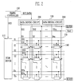
- FIG. 2 illustrates a schematic diagram of a light emitting display according to an embodiment of the present invention
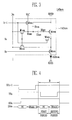
- FIG. 3 illustrates a circuit diagram of an exemplary pixel employable in the light emitting display illustrated in FIG. 2;
- FIG. 4 illustrates exemplary waveforms employable for driving the pixel illustrated in FIG. 3;
- FIG. 5 illustrates a circuit diagram of another exemplary pixel employable in the light emitting display illustrated in FIG. 2;
- FIG. 6 illustrates a block diagram of a first embodiment of the data driving circuit illustrated in FIG. 2;
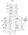
- FIG. 7 illustrates a block diagram of a second embodiment of the data driving circuit illustrated in FIG. 2;
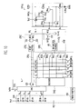
- FIG. 8 illustrates a schematic diagram of a first embodiment of a connection scheme connecting a gamma voltage unit, a digital-to-analog converter, a decoder, a voltage controller, a switching unit and a current sink unit illustrated in FIG. 6, and a pixel illustrated in FIG. 3;
- FIG. 9 illustrates exemplary waveforms employable for driving the pixel, the switching unit and the current sink unit illustrated in FIG. 8;
- FIG. 10 illustrates the connection scheme illustrated in FIG. 8 employing another embodiment of a switching unit
- FIG. 11 illustrates a schematic diagram of a second embodiment of a connection scheme connecting the gamma voltage unit, the digital-to-analog converter, the decoder, the voltage controller, the switching unit and the current sink unit illustrated in FIG. 6, and the pixel illustrated in FIG. 5.
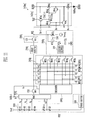
- FIG. 2 illustrates a schematic diagram of a light emitting display according to an embodiment of the present invention.
- the light emitting display may include a scan driver 110, a data driver 120, a pixel unit 130 and a timing controller 150.
- the pixel unit 130 may include a plurality of pixels 140.
- the pixel unit 130 may include n x m pixels 140 arranged, for example, in n rows and m columns, where n and m may each be integers.
- the pixels 140 may be connected to scan lines S1 to Sn, emission control lines E1 to En and data lines D1 to Dm.
- the pixels 140 may be respectively formed in the regions partitioned by the emission control lines En1 to En and the data lines D1 to Dm.
- the scan driver 110 may drive the scan lines S1 to Sn and the emission control lines E1 to En.
- the data driver 120 may drive the data lines D1 to Dm.
- the timing controller 150 may control the scan driver 110 and the data driver 120.
- the data driver 120 may include one or more data driving circuits 200.
- the timing controller 150 may generate data driving control signals DCS and scan driving control signals SCS in response to externally supplied synchronizing signals (not shown).
- the data driving control signals DCS generated by the timing controller 150 may be supplied to the data driver 120.
- the scan driving control signals SCS generated by the timing controller 150 may be supplied to the scan driver 110.
- the timing controller 150 may supply first data DATA1 to the data driver 120 in accordance with the externally supplied data (not shown).
- the scan driver 110 may receive the scan driving control signals SCS from the timing controller 150.
- the scan driver 110 may generate scan signals SS1 to SSn based on the received scan driving control signals SCS and may sequentially and respectively supply the scan signals SS1 to SSn to the scan lines S1 to Sn.
- the scan driver 110 may sequentially supply emission control signals ES1 to ESn to the emission control lines E1 to En.
- Each of the emission control signals ES1 to ESn may be supplied, e.g., changed from a low voltage signal to a high voltage signal, such that an "on" emission control signal, e.g., a high voltage signal, at least partially overlaps at least two of the scan signals SS1 to SSn. Therefore, in embodiments of the invention, a pulse width of the emission control signals ES1 to ESn may be equal to or larger than a pulse width of the scan signals SS1 to SSn.
- the data driver 120 may receive the data driving control signals DCS from the timing controller 150.
- the data driver 120 may generate data signals DS1 to DSm based on the received data driving control signals DCS and the first data DATA1.
- the generated data signals DS1 to DSm may be supplied to the data lines D1 to Dm in synchronization with the scan signals SS1 to SSn supplied to the scan lines S1 to Sn.
- the generated data signals DS1 to DSm corresponding to the pixels 140(1)(1 to m) may be synchronously supplied to the 1 st to the m-th pixels in the 1 st row via the data lines D1 to Dm
- the generated data signals DS1 to DSm corresponding to the pixels 140(n)(1 to m) may be synchronously supplied to the 1 st to the m-th pixels in the n-th row via the data lines D1 to Dm.
- the data driver 120 may supply predetermined currents to the data lines D1 to Dm during a first period of one horizontal period 1H for driving one or more of the pixels 140.
- one horizontal period 1H may correspond to a complete period associated with one of the scan signals SS1 to SSn and a corresponding one of the data signals DS1 to DSm being supplied to the respective pixel 140 in order to drive the respective pixel 140.
- the data driver 120 may supply predetermined voltages to the data lines D1 to Dm during a second period of the one horizontal period.
- one horizontal period 1H may correspond to a complete period associated with one of the scan signals SS1 to SSn and a corresponding one of the data signals DS1 to DSm being supplied to the respective pixel 140 in order to drive the respective pixel 140.
- the data driver 120 may include at least one data driving circuit 200 for supplying such predetermined currents and predetermined voltages during the first and second periods of one horizontal period 1H.
- the predetermined voltages that may be supplied to the data lines D1 to Dm during the second period will be referred to as the data signals DS1 to DSm.
- the pixel unit 130 may be connected to a first power source ELVDD for supplying a first voltage VDD, a second power source ELVSS for supplying a second voltage VSS and a reference power source EL Vref for supplying a reference voltage Vref to the pixels 140.
- the first power source ELVDD, the second power source ELVSS and the reference power source EL Vref may be externally provided.
- the pixels 140 may receive the first voltage VDD signal and the second voltage VSS signal, and may control the currents that flow through respective light emitting devices/materials, e.g., OLEDs, in accordance with the data signals DS1 to DSm that may be supplied by the data driver 120 to the pixels 140.
- the pixels 140 may thereby generate light components corresponding to the received first data DATA1.
- the pixels 140 may receive the first voltage VDD signal, the second voltage VSS signal and the reference voltage Vref signal from the respective first, second and reference power sources ELVDD, ELVSS and ELVref.
- the pixels 140 may compensate for a voltage drop in the first voltage VDD signal and/or threshold voltage(s) using the reference voltage Vref signal. The amount of compensation may be based on a difference between voltage values of the reference voltage Vref signal and the first voltage VDD signal respectively supplied by the reference power source ELVref and the first power source ELVDD.
- the pixels 140 may supply respective currents from the first power source ELVDD to the second power source ELVSS via, e.g., the OLEDs in response to the respective data signals DS1 to DSm.
- each of the pixels 140 may have, for example, the structure illustrated in FIG. 3 or 5.
- FIG. 3 illustrates a circuit diagram of an nm-th exemplary pixel 140nm employable in the light emitting display illustrated in FIG. 2.
- FIG. 3 illustrates the nm-th pixel that may be the pixel provided at the intersection of the n-th row of scan lines Sn and the m-th row of data lines Dm.
- the nm-th pixel 140nm may be connected to the m-th data line Dm, the n-1th and nth scan lines Sn-1 and Sn and the nth emission control line En.
- FIG. 3 only illustrates one exemplary pixel 140nm.
- the structure of the exemplary pixel 140nm may be employed for all or some of the pixels 140 of the light emitting display.
- the nm-th pixel 140nm may include a light emitting material/device, e.g., OLEDnm, and an nm-th pixel circuit 142nm for supplying current to the associated light emitting material/device.
- a light emitting material/device e.g., OLEDnm
- an nm-th pixel circuit 142nm for supplying current to the associated light emitting material/device.
- the nm-th OLEDnm may generate light of a predetermined color in response to the current supplied from the nm-th pixel circuit 142nm.
- the nm-th OLEDnm may be formed of, e.g., organic material, phosphor material and/or inorganic material.
- the nm-th pixel circuit 142nm may generate a compensation voltage for compensating for variations within and/or among the pixels 140 such that the pixels 140 may display images with uniform brightness.
- the nm-th pixel circuit 142nm may generate the compensation voltage using a previously supplied scan signal of the scan signals SS1 to SSn during each scan cycle.
- one scan cycle may correspond to scan signals SS1 to SSn being sequentially supplied.
- the n-1th scan signal SSn-1 may be supplied prior to the nth scan signal SSn and when the n-1th scan signal SSn-1 is being supplied to the n-1th scan line of the light emitting display, the nm-th pixel circuit 142nm may employ the n-1th scan signal SSn-1 to generate a compensation voltage.
- the second pixel in the second column i.e., the pixel 140 22 , may generate a compensation voltage using the first scan signal SS1.
- the compensation voltage may compensate for a voltage drop in a source voltage signal and/or a voltage drop resulting from a threshold voltage of the transistor of the nm-th pixel circuit 142nm.
- the nm-th pixel circuit 142nm may compensate for a voltage drop of the first voltage VDD signal and/or a threshold voltage of a transistor, e.g., a threshold voltage of a fourth transistor M4nm of the pixel circuit 142nm based on the compensation voltage that may be generated using a previously supplied scan line during the same scan cycle.
- the pixel circuit 142nm may compensate for a drop in the voltage of the first power source ELVDD and the threshold voltage of the fourth transistor M4nm when the n-1th scan signal SSn-1 is supplied to the n-1th scan line Sn-1, and may charge the voltage corresponding to the data signal DSm when the nth scan signal SSn is supplied to the nth scan line Sn.
- the pixel circuit 142nm may include first to sixth transistors M1nm to M6nm, a first capacitor C1nm and a second capacitor C2nm to generate the compensation voltage and to drive the light emitting material/device.
- a first electrode of the first transistor M1nm may be connected to the data line Dm and a second electrode of the first transistor M1nm may be connected to a first node N1nm.
- a gate electrode of the first transistor M1nm may be connected to the nth scan line Sn.
- the first transistor M1nm may be turned on when the nth scan signal SSn is supplied to the nth scan line Sn.
- the data line Dm may be electrically connected to the first node N1nm.
- a first electrode of the first capacitor C1nm may be connected to the first node N1nm and a second electrode of the first capacitor C1nm may be connected to the first power source ELVDD.
- a first electrode of the second transistor M2nm may be connected to the data line Dm and a second electrode of the second transistor M2nm may be connected to a second electrode of the fourth transistor M4nm.
- a gate electrode of a second transistor M2nm may be connected to the nth scan line Sn.
- the second transistor M2nm may be turned on when the nth scan signal SSn is supplied to the nth scan line Sn.
- the data line Dm may be electrically connected to the second electrode of the fourth transistor M4nm.
- a first electrode of the third transistor M3nm may be connected to the reference power source EL Vref and a second electrode of the third transistor M3nm may be connected to the first node N1nm.
- a gate electrode of the third transistor M3nm may be connected to the n-1th scan line Sn-1.
- the third transistor M3nm may be turned on when the n-1th scan signal SSn-1 is supplied to the n-1th scan line Sn-1.
- the reference voltage Vref may be electrically connected to the first node N1nm.
- a first electrode of the fourth transistor M4nm may be connected to the first power source ELVDD and the second electrode of the fourth transistor M4nm may be connected to a first electrode of the sixth transistor M6nm.
- a gate electrode of the fourth transistor M4nm may be connected to the second node N2nm.
- a first electrode of the second capacitor C2nm may be connected to the first node N1nm and a second electrode of the second capacitor C2nm may be connected to the second node N2nm.
- the first and second capacitors C1nm and C2nm may be charged when the n-1th scan signal SSn-1 is supplied.
- the first and second capacitors C1nm and C2nm may be charged and the fourth transistor M4nm may supply a current corresponding to a voltage at the second node N2nm to the first electrode of the sixth transistor M6nm.
- a second electrode of the fifth transistor M5nm may be connected to the second node N2nm and a first electrode of the fifth transistor M5nm may be connected to the second electrode of the fourth transistor M4nm.
- a gate electrode of the fifth transistor M5nm may be connected to the n-1th scan line Sn-1.
- the fifth transistor M5nm may be turned on when the n-1th scan signal SSn-1 is supplied to the n-1th scan line Sn-1 so that current flows through the fourth transistor M4nm. Therefore, the fourth transistor M4nm may operate as a diode.
- the first electrode of the sixth transistor M6nm may be connected to the second electrode of the fourth transistor M4nm and a second electrode of the sixth transistor M6nm may be connected to an anode electrode of the nm-th OLEDnm.
- a gate electrode of the sixth transistor M6nm may be connected to the nth emission control line En.
- the sixth transistor M6nm may be turned off when an emission control signal ESn is supplied, e.g., a high voltage signal, to the nth emission control line En and may be turned on when no emission control signal, e.g., a low voltage signal, is supplied to the nth emission control line En.
- the emission control signal ESn supplied to the nth emission control line En may be supplied to at least partially overlap both the n-1th scan signal SSn-1 that may be supplied to the n-1th scan line Sn-1 and the nth scan signal SSn that may be supplied to nth scan line Sn.
- the sixth transistor M6nm may be turned off when the n-1th scan signal SSn-1 is supplied, e.g., a low voltage signal is supplied, to the n-1th scan line Sn-1 and the n-th scan signal SSn is supplied, e.g., a low voltage signal is supplied, to the nth scan line Sn so that a predetermined voltage may be charged in the first and second capacitors C1nm and C2nm.
- the sixth transistor M6nm may be turned on during other times to electrically connect the fourth transistor M4nm and the nm-th OLEDnm to each other. In the exemplary embodiment shown in FIG.
- the transistors M1nm to M6nm are PMOS transistors, which may turn on when a low voltage signal is supplied to the respective gate electrode and may turn on when a high voltage signal is supplied to the respective gate electrode.
- PMOS transistors may turn on when a low voltage signal is supplied to the respective gate electrode and may turn on when a high voltage signal is supplied to the respective gate electrode.
- embodiments of the present invention are not limited to the use of PMOS devices.
- the voltage value of the reference voltage Vref may be equal to or different from the first voltage ELVDD.
- FIG. 4 illustrates exemplary waveforms that may be employed for driving the exemplary nm-th pixel 140nm illustrated in FIG. 3.
- each horizontal period 1H for driving the nm-th pixel 140nm may be divided into a first period and a second period.
- predetermined currents PCs
- the data signals DS1 to DSm may be supplied to the respective pixels 140 via the data lines D1 to Dm.
- the respective PCs may be supplied from each of the pixel(s) 140 to a data driving circuit 200 that may be capable of functioning, at least in part, as a current sink.
- the data signals DS 1 to DSm may be supplied from the data driving circuit 200 to the pixel(s) 140.
- the voltage value of the reference voltage Vref signal is equal to the voltage value of the first voltage VDD signal.
- the n-1th scan signal SSn-1 may be supplied to the n-1th scan line Sn-1 to control the on/off operation of the m pixels that may be connected to the n-1th scan line Sn-1.
- the scan signal SSn-1 is supplied to the n-1th scan line Sn-1, the third and fifth transistors M3nm and M5nm of the nm-th pixel circuit 142nm of the nm pixel 140nm may be turned on.
- the fourth transistor M4nm When the fifth transistor M5nm is turned on, current may flow through the fourth transistor M4nm so that the fourth transistor M4nm may operate as a diode.
- the voltage value of the second node N2nm may correspond to a difference between the threshold voltage of the fourth transistor M4nm and the voltage of the first voltage VDD signal being supplied by the first power source ELVDD.
- the reference voltage Vref signal from the reference power source ELVref may be applied to the first node N1nm.
- the second capacitor C2nm may be charged with a voltage corresponding to the difference between the first node N1nm and the second node N2nm.
- the reference voltage Vref signal from the reference power source EL Vref and the first voltage VDD from the first power source ELVDD may, at least initially, i.e., prior to any voltage drop that may result during operation of the pixels 140, be equal, the voltage corresponding to the threshold voltage of the fourth transistor M4nm may be charged in the second capacitor C2nm.
- the threshold voltage of the fourth transistor M4nm and a voltage corresponding to the magnitude of the voltage drop of the first power source ELVDD may be charged in the second capacitor C2nm.
- a predetermined voltage corresponding to the sum of the voltage corresponding to the voltage drop of the first voltage VDD signal and the threshold voltage of the fourth transistor M4nm may be charged in the second capacitor C2nm.
- the voltage corresponding to the sum of the threshold voltage of the fourth transistor M4nm and the difference between the reference voltage signal Vref and the first voltage VDD signal may be charged in the second capacitor C2nm before the nth scan signal SSn is supplied to the nth scan line Sn.
- the first and second transistors M1nm and M2nm may be turned on.
- the PC may be supplied from the nm-th pixel 140nm to the data driving circuit 200 via the data line Dm.
- the PC may be supplied to the data driving circuit 200 via the first power source ELVDD, the fourth transistor M4nm, the second transistor M2nm and the data line Dm.
- a predetermined voltage may then be charged in the first and second capacitors C1nm and C2nm in response to the supplied PC.
- the data driving circuit 200 may reset a voltage of a gamma voltage unit (not shown) based on a predetermined voltage value, i.e., compensation voltage that may be generated when the PC sinks, as described above.
- the reset voltage from the gamma voltage unit (not shown) may be used to generate the data signals DS1 to DSm to be respectively supplied to the data lines D 1 to Dm.
- the generated data signals DS1 to DSm may be respectively supplied to the respective data lines D1 to Dm during the second period of the one horizontal period. More particularly, e.g., the respective generated data signal DSm may be supplied to the respective first node N1nm via the first transistor M1nm during the second period of the one horizontal period. Then, the voltage corresponding to difference between the data signal DSm and the first power source ELVDD may be charged in the first capacitor C1nm. The second node N2nm may then float and the second capacitor C2nm may maintain the previously charged voltage.
- a voltage corresponding to the threshold voltage of the fourth transistor M4nm and the voltage drop of the first voltage VDD signal from the first power source ELVDD may be charged in the second capacitor C2nm of the nm-th pixel 140nm to compensate for the voltage drop of the first voltage VDD signal from the first power source ELVDD and the threshold voltage of the fourth transistor M4nm.
- the voltage of the gamma voltage unit (not shown) may be reset so that the electron mobility of the transistors included in the respective n-th pixels 140n associated with each data line D 1 to Dm may be compensated for and the respective generated data signals DS1 to DSm may be supplied to the n-th pixels 140n using the respective reset gamma voltages. Therefore, in embodiments of the invention, non-uniformity in the threshold voltages of the transistors and the electron mobility may be compensated, and images with uniform brightness may be displayed. Processes for resetting the voltage of the gamma voltage unit will be described below.
- FIG. 5 illustrates another exemplary embodiment of an nm-th pixel 140nm' employable by the light emitting display illustrated in FIG. 2.
- the structure of the nm-th pixel 140nm' illustrated in FIG. 5 is substantially the same as the structure of the nm-th pixel 140nm illustrated in FIG. 3, but for the arrangement of a first capacitor C1nm' in a pixel circuit 142nm' and respective connections to a first node N1nm' and a second node N2nm'.
- a first electrode of the first capacitor C1nm' may be connected to the second node N2nm' and a second electrode of the first capacitor C1nm' may be connected to the first power source ELVDD.
- a first electrode of the second capacitor C2nm may be connected to the first node N1nm' and a second electrode of the second capacitor C2nm may be connected to the second node N2nm'.
- the first node N1nm' may be connected to the second electrode of the first transistor M1nm, the second electrode of the third transistor M3nm and the first electrode of the second capacitor C2nm.
- the second node N2nm' may be connected to the gate electrode of the fourth transistor M4nm, the second electrode of the fifth transistor M5nm, the first electrode of the first capacitor C1nm' and the second electrode of the second capacitor C2nm.
- Exemplary methods for operating the nm-th pixel circuit 142nm' of the nm-th pixel 140nm' of the pixels 140 will be described in detail with reference to FIGS. 4 and 5.
- the third and fifth transistors M3nm and M5nm of the n-th pixel(s) 140(n)(1 to m), i.e., the pixels arranged in the n-th row may be turned on.
- the fourth transistor M4nm When the fifth transistor M5nm is turned on, current may flow through the fourth transistor M4nm so that the fourth transistor M4nm may operate as a diode.
- a voltage corresponding to a value obtained by subtracting the threshold voltage of the fourth transistor M4nm from the first power source ELVDD may be applied to a second node N2nm'.
- the voltage corresponding to the threshold voltage of the fourth transistor M4nm may be charged in the first capacitor C1nm'.
- the first capacitor C1nm' may be provided between the second node N2nm' and the first power source ELVDD.
- the third transistor M3nm When the third transistor M3nm is turned on, the voltage of the reference power source EL Vref may be applied to the first node N1nm'. Then, the second capacitor C2nm may be charged with the voltage corresponding to difference between a first node N1nm' and the second node N2nm'. During the period where the n-1th scan signal SSn-1 is supplied to the n-1th scan line Sn-1 and the first and second transistors M1nm and M2nm may be turned off, the data signal DSm may not be supplied to the nm-th pixel 140nm'.
- the scan signal SSn may be supplied to the nth scan line Sn and the first and second transistors M1nm and M2nm may be turned on.
- the respective PC may be supplied from the nm-th pixel 140nm' to the data driving circuit 200 via the data line Dm.
- the PC may be supplied to the data driving circuit 200 via the first power source ELVDD, the fourth transistor M4nm, the second transistor M2nm and the data line Dm.
- predetermined voltage may be charged in the first and second capacitors C1nm' and C2nm.
- the data driving circuit 200 may reset the voltage of the gamma voltage unit using the compensation voltage applied in response to the PC to generate the data signal DS using the respectively reset voltage of the gamma voltage unit.
- the data signal DSm may be supplied to the first node N1nm'.
- the predetermined voltage corresponding to the data signal DSm may be charged in the first and second capacitors C1nm' and C2nm.
- the voltage of the first node N1nm' may fall from the voltage Vref of the reference power source EL Vref to the voltage of the data signal DSm.
- the voltage value of the second node N2nm' may be reduced in response to the amount of voltage drop of the first node N1nm'.
- the amount of reduction in voltage that may occur at the second node N2nm' may be determined by the capacitances of the first and second capacitors C1nm' and C2nm.
- the predetermined voltage corresponding to the voltage value of the second node N2nm' may be charged in the first capacitor C1nm'.
- the voltage value of the reference power source EL Vref is fixed, the amount of voltage charged in the first capacitor C1nm' may be determined by the data signal DSm. That is, in the nm-th pixel 140nm' illustrated in FIG. 5, because the voltage values charged in the capacitors C1nm' and C2nm may be determined by the reference power source EL Vref and the data signal DSm, it may be possible to charge a desired voltage irrespective of the voltage drop of the first power source ELVDD.
- the voltage of the gamma voltage unit may be reset so that the electron mobility of the transistors included in each of the pixels 140 may be compensated for and the respective generated data signal may be supplied using the reset gamma voltage.
- non-uniformity among the threshold voltages of the transistors and deviation in the electron mobility of the transistors may be compensated for, thereby enabling images with uniform brightness to be displayed.
- FIG. 6 illustrates a block diagram of a first exemplary embodiment of the data driving circuit illustrated in FIG. 2.
- the data driving circuit 200 has j channels, where j is a natural number equal to or greater than 2.
- the data driving circuit 200 may include a shift register unit 210, a sampling latch unit 220, a holding latch unit 230, a decoder unit 240, a digital-analog converter unit (hereinafter, referred to as a a DAC) 250, a voltage controller unit 260, a first buffer unit 270, a current supply unit 280, a selector 290 and a gamma voltage unit 300.
- a shift register unit 210 may include a shift register unit 210, a sampling latch unit 220, a holding latch unit 230, a decoder unit 240, a digital-analog converter unit (hereinafter, referred to as a a DAC) 250, a voltage controller unit 260, a first buffer unit 270, a current supply unit 280, a selector 290 and a gamma voltage unit 300.
- a DAC digital-analog converter unit
- the shift register unit 210 may receive a source shift clock SSC and a source start pulse SSP from the timing controller 150.
- the shift register unit 210 may utilize the source shift clock SSC and the source start pulse SSP to sequentially generate j sampling signals while shifting the source start pulse SSP every one period of the source shift clock SSC.
- the shift register unit 210 may include j shift registers 2101 to 210j.
- the sampling latch unit 220 may sequentially store the respective first data DATA1 in response to sampling signals sequentially supplied from the shift register unit 210.
- the sampling latch unit 220 may include j sampling latches 2201 to 220j in order to respectively store the j first data DATA1-1 to DATA1-j.
- Each of the sampling latches 2201 to 220j may have a magnitude corresponding to a number of bits of the first data DATA1. For example, when the first data DATA1 is k bits, each of the sampling latches 2201 to 220j may have a magnitude of k bits such that the sampling latches 2201 to 220j may respectively store k-bits of each of the j first DATA1-1 to DATA1-j.
- the holding latch unit 230 may receive the first data DATA1 from the sampling latch unit 220 to store the first data DATA1 when a source output enable SOE signal is input to the holding latch unit 230.
- the holding latch unit 230 may supply the first data DATA1 stored therein to the decoder unit 240 and/or the DAC unit 250 when the SOE signal is input.
- the holding latch unit 230 may include j holding latches 2301 to 230j in order to store the j first data DATA1-1 to DATA1-j.
- Each of the holding latches 2301 to 230j may have a magnitude corresponding to the number of bits of the first data DATA1.
- each of the holding latches 2301 to 230j may have a magnitude of k bits so that the k bits of each of the j first data DATA1-1 to DATA1-j may be respectively stored.
- the decoder unit 240 may include j decoders 2401 through 240j. Each of the decoders 2401 through 240j may receive k bits of the respective first data DATA1 and may convert the k bits of the first data DATA1 into p (p is a natural number) bits of second data DATA2. In embodiments of the invention, each of the decoders 2401 through 240j may generate p bits of second data DATA2 using a binary weighted value.
- the weighted value of the externally received first data DATA1 may be determined to allow the gamma voltage unit 300 to be set a predetermined voltage. For example, the number of bits of the first data DATA1 allowing a desired gray scale voltage to be selected from a plurality of gray scale voltages may be determined. The plurality of gray scale voltages may be generated by the gamma voltage unit 300.
- the decoders 2401 through 240j may convert k bits of the first data DATA1, corresponding to the gray scale voltages, into respective p bits of second data DATA2-1 to DATA2-j using a binary weighted value. For example, the decoders 2401 through 240j may generate five bits of the second data DATA2 using eight bits of the first data DATA1.
- the current supply unit 280 may sink predetermined current PC from the respective pixel(s) 140 selected by one of the scan signals SS1 to SSn.
- the current supply unit 280 may receive the sinking current via the respective one of the data lines D1 through Dj, during the first period of each horizontal period.
- the current supply unit 280 may sink an amount of current corresponding to a minimum amount of current that may be employed by the respective light emitter, e.g., OLED, to emit light of maximum brightness. Then, the current supply unit 280 may supply a predetermined compensation voltage to the voltage controller unit 260. The compensation voltage may be generated while the respective predetermined current PC was sinking.
- the current supply unit 280 includes j current sink units 2801 through 280j.
- the gamma voltage unit 300 may generate predetermined gray scale voltages corresponding to the k bits of the first data DATA1.
- the gamma voltage unit 300 may include a plurality of distribution or voltage dividing resistors R1 through R l and may generate 2 k gray scale voltages.
- the gray scale voltages generated by the gamma voltage unit 300 may be supplied to the DAC unit 250.
- the DAC unit 250 may include j DACs 2501 through 250j.
- the gray scale voltages generated by the gamma voltage unit 300 may be supplied to each of the j DACs 2501 through 250j.
- Each of the DACs 2501 through 250j may select, as a data signal DS, one of the gray scale voltages that may be supplied by the gamma voltage unit 300 based on the respective first data DATA1-1 to DATA1-j supplied from the respective holding latch units 2301 through 230j.
- the DACs 2501 to 250j may respectively select, as a data signal DS, one of the gray scale voltages that may be supplied by the gamma voltage unit 300 based on a number of bits of the respective first data DATA1-1 to DATA1-j.
- the voltage controller unit 260 may include j voltage controllers 2601 through 260j.
- the voltage controllers 2601 through 260j may each receive a compensation voltage, e.g., voltage supplied via the respective current sink unit 2801-280j or the second data DATA2, and a third supply voltage signal VSS'.
- a compensation voltage e.g., voltage supplied via the respective current sink unit 2801-280j or the second data DATA2
- a third supply voltage signal VSS' may be employed for supplying the second voltage VSS signal and the third supply voltage VSS' signal.
- the third supply voltage VSS' signal may be supplied to a terminal of the gamma voltage unit 300.
- the voltage controllers 2601 through 260j which may receive the compensation voltage and/or the second data DATA2, and the third supply voltage VSS' signal, may control a voltage value of the selected data signal DS so that variations among the pixels 140, such as, variations due to electron mobility, threshold voltage, etc. of transistors included in the respective pixels 140 may be compensated for.
- the first buffer unit 270 may supply the respective data signal DS to the selector 290. As discussed above, the voltage of the respective data signal may be controlled by the voltage control unit 260. In embodiments of the invention, the first buffer unit 270 may include j first buffers 2701 through 274j.
- the selector 290 may control electrical connections between the data lines D1 to Dj and the first buffers 2701 to 270j.
- the selector 290 may electrically connect the data lines D1 to Dj and the first buffers 2701 to 270j to each other during the second period of the one horizontal period.
- the selector 290 may electrically connect the data lines D1 to Dj and the first buffers 2701 to 270j to each other only during the second period. During periods other than the second period, the selector 290 may keep the data lines D1 to Dj and the first buffers 2701 to 270j electrically disconnected from each other.
- the selector 290 may include j switching units 2901 to 290j.
- the generated respective data signals DS1 to DSj may be respectively supplied from the first buffers 2701 to 270j to the data lines D1 to Dj via the switching units 2901 to 290j.
- the selection unit 290 may employ other types of switching units.
- Fig. 10 illustrates another exemplary embodiment of a switching unit switching unit 290j' that may be employed by the selector 290.
- the data driving circuit 200 may include a level shifter 310 that is connected to the holding latch unit 230.
- the level shifter 310 may include level registers 3101 to 310j and may raise the voltage of the first data DATA1 that may be supplied from the holding latch unit 230 and may supply the level-shifted result to the DAC unit 250 and the decoder unit 240.
- the data (not shown) being supplied from an external system to the data driving circuit 200 has high voltage levels, circuit components with high voltage resistant properties should generally be provided, thus, increasing the manufacturing cost.
- the data being supplied from an external system to the data driving circuit 200 may have low voltage levels and the low voltage level may be transitioned to a high voltage level by the level shifter 310.
- FIG. 8 illustrates a first embodiment of a connection scheme for connecting the gamma voltage unit 300, the DAC 250j, the decoder 240j, the voltage controller 260j, the switching unit 290j, the current sink unit 280j, and a pixel 140nj.
- FIG. 8 only illustrates one channel, i.e., the jth channel and it is assumed that the data line Dj is connected to an nj-th pixel 140nj according to the exemplary embodiment of the pixel 140nm illustrated in FIG. 3.
- the gamma voltage unit 300 may include a plurality of distribution resistors R1 to R l.
- the distribution resistors R1 to R l may be disposed between the reference supply voltage Vref and the third supply voltage VSS'.
- the distribution resistors R1 to R l may distribute or divide a voltage supplied thereto.
- the distribution resistors R1 to R l may distribute or divide a voltage between the reference supply voltage Vref and the third supply voltage VSS', and may generate a plurality of gray scale voltages V0 through V2 K -1.
- the distribution resistors R1 to R l may supply the generated gray scale voltages V0 through V2 K -1 to the DAC 250j.
- the gamma voltage unit 300 may supply the third supply voltage VSS' to the voltage controller 260j via a third buffer 301.
- the DAC 250j may select, as a data signal DS, one of the gray scale voltages V0 through V2 K -1, based on a number of the bits of the first data DATA1 and may supply the selected voltage to a first buffer 270j.
- a transistor e.g., forty-first transistor M41, which may be controlled by a third control signal CS3, may be disposed between the DAC 250j and the first buffer 270j.
- the forty-first transistor M41 may be turned on at a predetermined time during the first period of the horizontal period for driving the pixel 140nj and the forty-first transistor M41 may supply the data signal DSj supplied from the DAC 250 to the first buffer 270j.
- the third control signal CS3 may rise after a second control signal CS2, which will be described below, and may fall at the same time as the second control signal CS2.
- the current sink unit 280j may include a twelfth transistor M12j and a thirteenth transistor M13j, a current source Imaxj, a third capacitor C3j, a third node N3j, a ground voltage source GND and a second buffer 281.
- the twelfth transistor M12j and the thirteenth transistor M13j may be controlled by the second control signal CS2.
- the current source Imaxj may be connected to a first electrode of the thirteenth transistor M13j.
- the third capacitor C3j may be connected between the third node N3j and the ground voltage source GND.
- the second buffer 281j may be connected between the third node N3j and the voltage controller 260j.
- a gate electrode of the twelfth transistor M12j may be connected to a gate electrode of the thirteenth transistor M13j.
- a second electrode of the twelfth transistor M12j may be connected to a second electrode of the thirteenth transistor M13j and the data line Dj.
- a first electrode of the twelfth transistor M12j may be connected to the second buffer 281.
- the twelfth transistor M12j and the thirteenth transistor M13j may be turned on during the first period of each horizontal period 1H.
- the twelfth transistor M12j and the thirteenth transistor M13j may be turned off during the second period of the horizontal period 1H.
- the second control signal CS2 may control the on/off state of the twelfth transistor M12j and the thirteenth transistor M13j.
- the current source Imaxj may receive, from the pixel 140nj, at least a minimum amount of current that may be supplied to the light emitter, e.g., OLEDnj, for the pixel 140nj to emit light with maximum brightness.
- the second control signal CS2 may control the twelfth transistor M12j and the thirteenth transistor M13j to be on during the first period, thereby allowing the predetermined current PC to flow from the pixel 140nj to the current sink unit 280j.
- the third capacitor C3j may store a compensation voltage that may be applied to the third node N3j when the current from the pixel 140nj sinks to the current source Imaxj.
- the third capacitor C3j may store the compensation voltage applied to the third node N3j during the first period of one horizontal period 1H, and may maintain the compensation voltage at the third node N3j stable even when the twelfth transistor M13 and the thirteenth transistor M13 are turned off.
- the second buffer 281j may transfer the compensation voltage applied to the third node N3j to the voltage controller 260j.
- the decoder 240j may receive and may convert k bits of the first data DATA1 into p bits of second data DATA2 using a binary weighted value.
- the decoder 240j may supply an initialization signal (not shown) to the voltage controller 260j during the first period of the horizontal period 1H and the decoder 240j may supply the p bits of second data DATA2 to the voltage controller 260j during the second period of the same horizontal period 1H.
- the p bits are 5 bits. In embodiments of the invention, p may be any integer greater than or equal to zero.
- the voltage controller 260j may receive the compensation voltage and/or the second data DATA2, and the third supply voltage VSS' and may control the voltage value of the data signal DSj.
- reference term “p” will be equal to five, however, “p” may be any integer.
- the voltage controller 260j may include p capacitors Cj, 2Cj, 4Cj, 8Cj and 16Cj, p PMOS transistors M31j, M32j, M33j, M34j and M35j and p NMOS transistors M21j, M22j, M23j, M24j and M25j.
- the capacitors Cj, 2Cj, 4Cj, 8Cj and 16Cj may be connected to an electrical path connecting the forty-first transistor M41 and the first buffer 270j.
- the p PMOS transistors M31j, M32j, M33j, M34j and M35j may be connected the third buffer 301 and the p capacitors Cj, 2Cj, 4Cj, 8Cj and 16Cj, respectively.
- the p NMOS transistors M21j, M22j, M23j, M24j and M25j may be connected between the second buffer 281j and the p capacitors Cj, 2Cj, 4Cj, 8Cj and 16Cj, respectively.
- Capacitance values of the p capacitors Cj, 2Cj, 4Cj, 8Cj and 16Cj may be relative to each other such that the capacitances of the p capacitors may increase along the order of 2 0 , 2 1 , 2 2 , 2 3 and 2 4 , respectively.
- the capacitances of the p capacitors Cj, 2Cj, 4Cj, 8Cj and 16Cj may have respective binary weighted values in accordance with the second data DATA2.
- the p PMOS transistors M31j, M32j, M33j, M34j and M35j may be respectively disposed between the p capacitors Cj, 2Cj, 4Cj, 8Cj and 16Cj and the third buffer 301.
- the p PMOS transistors M31j, M32j, M33j, M34j and M35j may be turned on when the initialization signal (not shown) is supplied from the decoder 240j, and the p PMOS transistors M31j, M32j, M33j, M34j and M35j may respectively set a voltage of a terminal of the p capacitors Cj, 2Cj, 4Cj, 8Cj and 16Cj to the third supply voltage VSS'.
- the p NMOS transistors M21j, M22j, M23j, M24j and M25j may be respectively disposed between each of the p capacitors Cj, 2Cj, 4Cj, 8Cj and 16Cj and the second buffer 281j.
- the p NMOS transistors M21j, M22j, M23j, M24j and M25j may be turned on or off during the second period of one horizontal period 1H for driving the pixel 140nj based on the second data DATA2 generated from the decoder 240j.
- the p NMOS transistors M21j, M22j, M23j, M24j and M25j may be controlled to select the respective one/ones of the p capacitors Cj, 2Cj, 4Cj, 8Cj and 16Cj based on bit weighted values of the second data DATA2. For example, if the bits of the second data DATA2 generated by the decoder 240j are set to "00011", the twenty-fourth transistor M24j and the twenty-fifth transistor M25 are turned on to apply the compensation voltage, e.g., voltage stored in the third capacitor C3j, to terminals of the respective first and second ones, e.g., Cj and 2Cj, of the p capacitors.
- the compensation voltage e.g., voltage stored in the third capacitor C3j
- the on/off state of the p NMOS transistors M21j, M22j, M23j, M24j and M25j may be controlled so that a compensation voltage may be applied to respective terminals of the first and second ones Cj and 2Cj of the p capacitors Cj, 2Cj, 4Cj, 8Cj and 16Cj.
- the first and second ones Cj and 2Cj of the p capacitors Cj, 2Cj, 4Cj, 8Cj and 16Cj may have capacitances corresponding to 2 0 and 2 1 .
- the voltage value of the data signal DSj applied to the electrical path between the forty-first transistor M41j and the first buffer 270j may be increased or decreased in accordance with the compensation voltage that may be applied to respective terminals of the p capacitors Cj, 2Cj, 4Cj, 8Cj and 16Cj. More particularly, any increase or decrease in the voltage value of the data signal DSj applied to the electrical path between the forty-first transistor M41j and the first buffer 270j (and later to the data line Dj) may depend on the voltage value of the compensation voltage. Because the voltage value of the data signal DSj may be controlled with the applied compensation voltage, the voltage value of the data signal DSj may be controlled so that variations among the pixels 140 may be compensated for and the pixel unit 130 can display a uniform image.
- the voltage value of the data signal DSj may be controlled with the applied compensation voltage, variations in electron mobility and/or threshold voltages of transistors included in the pixel 140nj may be compensated for.
- the data driving circuit 200 may control the voltage value of the data signals DS using a compensation voltage generated based on characteristics, e.g., electron mobility, threshold voltage, etc., of the respective pixels 140, the data driving circuit may control the voltage value of the respective data signal DS being supplied to the respective pixels 140 and may can compensate for variations in electron mobility of the transistors.
- the first buffer 270j may transfer the data signal DSj applied to the electrical connection between the forty-first transistor M41j and the first buffer 270j to the switching unit 290j.
- the switching unit 290j may include an eleventh transistor M11j.
- the eleventh transistor M11j may be controlled by the first control signal CS1, as shown in FIGS. 8 and 9.
- the eleventh transistor M11j may be turned on during the second period of each horizontal period 1H for driving each of the n pixels in the j-th channel.
- the eleventh transistor M11j may be turned off during the first period of each horizontal period 1H for driving each of the n pixels in the j-th channel.
- the data signal DSj may supplied to the data line Dj during the second period of the horizontal period 1H and may not be supplied during other periods, e.g., the first period, of a single horizontal period 1H.
- the data signal DSj may only be supplied during the second horizontal period of a single horizontal period 1H. In embodiments of the invention, the data signal DSj may never be supplied to the data line Dj during the first period of a single horizontal period 1H.
- FIG. 9 illustrates exemplary waveforms employable for driving the pixel, the switching unit and the current sink unit illustrated in FIG. 8. Exemplary methods for controlling the voltage of data signals DS respectively supplied to the pixels 140 will be described in detail with reference to FIGS. 8 and 9.
- the pixel 140nj and the pixel circuit 142nj according to the exemplary embodiment illustrated in FIG. 3, is provided.
- the same reference numerals employed above in the description of the nm-th pixel 140nm shown in FIG. 3 will be employed to describe like features in the exemplary embodiment of the nj-th pixel 140nj illustrated in FIG. 8.
- the scan signal SSn-1 may be supplied to the n-1th scan line Sn-1.
- the third and fifth transistors M3nj and M5nj may be turned on.
- the voltage value obtained by subtracting the threshold voltage of the fourth transistor M4nj from the first power source ELVDD may then be applied to a second node N2nj and the voltage of the reference power source EL Vref may be applied to a first node N1nj.
- the voltage corresponding to the voltage drop of the first power source ELVDD and the threshold voltage of the fourth transistor M4nj may then be charged in the second capacitor C2nj.
- V N ⁇ 1 V ⁇ ref
- V N ⁇ 2 ELVDD ⁇ V th ⁇ M ⁇ 4
- V N1 , V N2 , and V thM4 represent the voltage applied to the first node N1nj, the voltage applied to the second node N2nj, and the threshold voltage of the fourth transistor M4nj, respectively.
- the first and second nodes N1nj and N2nj may be floating. Therefore, the voltage value charged in the second capacitor C2nj may not change during that time.
- the n-th scan signal SSn may then be supplied to the nth scan line Sn so that the first and second transistors M1nj and M2nj may be turned on.
- the 12 th and 13 th transistors M12j and M13j may be turned on.
- the current that may flow through the current source Imaxj via the first power source ELVDD, the fourth transistor M4nj, the second transistor M2nj, the data line Dj, and the 13 th transistor M13j may sink.
- EQUATION3 When current flows through the current source Imaxj via the first power source ELVDD, the fourth transistor M4nj and the second transistor M2nj, EQUATION3 may apply.
- I ⁇ max 1 2 ⁇ ⁇ p ⁇ C o ⁇ x ⁇ W L ⁇ ELVDD ⁇ V N ⁇ 2 ⁇ V th ⁇ M ⁇ 4 2
- ⁇ , Cox, W, and L represent the electron mobility, the capacity of an oxide layer, the width of a channel, and the length of a channel, respectively.
- V N ⁇ 2 ELVDD ⁇ 2 ⁇ I ⁇ max ⁇ p ⁇ C o ⁇ x ⁇ L W ⁇ V th ⁇ M ⁇ 4
- the voltage applied to the first node N1nj may be represented by EQUATION5 by the coupling of the second capacitor C2nj.
- the voltage V N1 may correspond to the voltage applied to the first node N1nj and the voltage V N3 may correspond to the voltage applied to the third node N3j.
- a voltage satisfying EQUATION5 may be applied to the third node N3j.
- the voltage applied to the third node N3j may be affected by the electron mobility of the transistors included in the pixel 140nj, which is supplying current to the current source Imaxj. Therefore, the voltage value applied to the third node N3j when the current is being supplied to the current source Imaxj may vary in each of the pixels 140, e.g., when the electron mobility varies in each of the pixels 140.
- the decoder 240j may supply an initialization signal during the first period of each horizontal period 1H.
- the initialization signal may turn on the thirty-first transistor M31j, the thirty-second transistor M32j, the thirty-third transistor M33j, the thirty-fourth transistor M34j and the thirty-fifth transistor M35j.
- a voltage of a terminal of each of the p capacitors Cj, 2Cj, 4Cj, 8Cj and 16Cj may be set to a voltage of the third supply voltage VSS'.
- the voltage value of the third supply voltage VSS' may be set lower than the voltage value of the reference supply voltage Vref.
- the third supply voltage VSS' may be set to an average voltage of compensation voltages that may be generated by the pixels 140 included in the pixel unit 130.
- a twenty-first transistor M21j, a twenty-second transistor M22j, a twenty-third transistor M23j, a twenty-fourth transistor M24j and a twenty-fifth transistor M25j may be turned on or off in accordance with the second data DATA2 that may be supplied from the decoder 240j.
- the decoder 240j may control the on/off state of the twenty-first transistor M21j, the twenty-second transistor M22j, the twenty-third transistor M23j, the twenty-fourth transistor M24j, and the twenty-fifth transistor M25j.
- the decoder 240j may control the on/off state of the twenty-first transistor M21j, the twenty-second transistor M22j, the twenty-third transistor M23j, the twenty-fourth transistor M24j, and the twenty-fifth transistor M25j to obtain a value approximating to a value of h/f in EQUATION6.
- the twenty-fourth transistor M24j and the twenty-fifth transistor M25j may be turned on to apply a compensation voltage to a terminal of each of the first and second ones Cj and 2Cj of the p capacitors.
- EQUATION7 can be deduced. EQUATION 7 C + 2 ⁇ C C + 2 ⁇ C + 4 ⁇ C + 8 ⁇ C + 16 ⁇ C ⁇ h f
- the second data DATA2 may be derived from the first data DATA1, a value satisfying EQUATION7 approximates the value of h/f.
- a voltage of the electrical connection between the forty-first transistor M41 and the first buffer 270j may be expressed by EQUATION8.
- a voltage satisfying EQUATION8 may be supplied to the eleventh transistor M11j via the first buffer 270j.
- the voltage supplied to the first buffer 270j may be supplied to the first node N1nj via the eleventh transistor M11j, the data line Dj, and the first transistor M1nj.
- the voltage satisfying EQUATION8 may be supplied to the first node N1nj.
- a voltage applied to the second node N2nj by coupling of the second capacitor C2nj can be expressed by EQUATION9.
- V N ⁇ 2 ELVDD ⁇ h f ⁇ 2 ⁇ I ⁇ max ⁇ p ⁇ C O ⁇ X ⁇ L W ⁇ V th ⁇ M ⁇ 4
- current flowing through the fourth transistor M4nj may be expressed by EQUATION10.
- current flowing through the fourth transistor M4nj may depend on the respective data signal DS supplied to the respective pixel 140 and more particularly, the gray scale voltage generated by the voltage controller 260j. Therefore, in embodiments of the invention, by supplying a current based on a compensation voltage generated by current sinking from the respective pixel 140nj, a desired current may be selected and supplied as the respective data signal DS, irrespective of threshold voltage, electron mobility, etc. of the transistors, e.g., M4nj, of the respective pixel. Thus, embodiments of the invention enable uniform images to be displayed irrespective of variations in electron mobility and threshold voltage within and among the pixels 140 of the pixel unit 130.
- FIG. 10 illustrates the connection scheme illustrated in FIG. 8 employing another embodiment of a switching unit 290j'.
- the exemplary connection scheme illustrated in FIG. 10 is substantially the same as the exemplary connection scheme illustrated in FIG. 8, but for another exemplary embodiment of the switching unit 290j'.
- the same reference numerals employed above will be employed to describe like features in the exemplary embodiment illustrated in FIG. 10.
- another exemplary switching unit 290j' may include eleventh and fourteenth transistors M11j, M14j that may be connected to each other in the form of a transmission gate.
- the 14 th transistor M14j which may be a PMOS type transistor, may receive the second control signal CS2.
- the eleventh transistor M11j which may be a NMOS type transistor, may receive the first control signal CS1.
- the eleventh and fourteenth transistors M11j and M14j may be turned on and off at the same time.
- a voltage-current characteristic curve may be in the form of a straight line and switching error may be minimized.
- FIG. 11 illustrates a second embodiment of a connection scheme for connecting the gamma voltage unit 300, the DAC 250j, the decoder 240j, the voltage controller 260j, the switching unit 290j, the current sink unit 280j, and a pixel 140nj'.
- FIG. 11 only illustrates one channel, i.e., the jth channel and it is assumed that the data line Dj is connected to the nj-th pixel 140nj' according to the exemplary embodiment of the pixel 140nm' illustrated in FIG. 5.
- the n-th scan signal may be applied to the n-th scan line Sn.
- w when the twelfth transistor M12j and the thirteenth transistor M13j may be turned on current flowing through the fourth transistor M4j may satisfy EQUATION3 and a voltage applied to the second node N2nj' may satisfy EQUATION4.
- EQUATION3 a voltage applied to the second node N2nj'
- a voltage applied to the first node N1nj' by coupling of the second capacitor C2nj can be expressed by EQUATION 11.
- the DAC 250j may select an h-th one of f gray scale voltages in accordance with the first data DATA1, where h and f are natural numbers.
- the DAC 250j may also supply a gray scale voltage satisfying EQUATION6.
- the selected h-th one of the f gray scale voltages may be supplied to first buffer 270j when the forty-first transistor M41 is turned on.
- the selected h-th one of the f gray scale voltages may be selected, as a respective data signal DSj to be supplied to the pixel 140nj' via the data line Dj.
- the decoder 240j may supply an initialization signal to the thirty-first transistor M31j, the thirty-second transistor M32j, the thirty-third transistor M33j, the thirty-fourth transistor M34j and the thirty-fifth transistor M35j and may thereby turn on each of the p transistors M31j, M32j, M33j, M34j and M35j during the first period of the horizontal period 1H for driving the pixel 140nj'.
- a voltage of a terminal of each of the p capacitors Cj, 2Cj, 4Cj, 8Cj and 16Cj may be to the third supply voltage VSS'.
- the twenty-first transistor M21j, the twenty-second transistor M22j, the twenty-third transistor M23j, the twenty-fourth transistor M24j and the twenty-fifth transistor M25j may be turned on or off in accordance with the second data DATA2 that may be supplied from the decoder 240j.
- the decoder 240j may control the turning on/off of the twenty-first transistor M21j, the twenty-second transistor M22j, the twenty-third transistor M23j, the twenty-fourth transistor M24j and the twenty-fifth transistor M25j.
- the decoder 240j may control the turning on/off of the twenty-first transistor M21j, the twenty-second transistor M22j, the twenty-third transistor M23j, the twenty-fourth transistor M24j and the twenty-fifth transistor M25j so as to obtain a value approximating to the value of h/f in EQUATION6.
- a voltage satisfying EQUATION12 may be supplied to the eleventh transistor M11j via the first buffer 270j.
- the voltage supplied to the first buffer 270j may be supplied to the first node N1nj' via the eleventh transistor M11j, the data line Dj and the first transistor M1j.
- a voltage satisfying EQUATION12 may be supplied to the first node N1nj'.
- a voltage applied to the second node N2nj' by the coupling of the second capacitor C2nj may be expressed by EQUATION9. Accordingly, current flowing through the fourth transistor M4nj may be expressed by EQUATION10.
- the current corresponding to the gray scale voltage selected by the DAC 250j may flow to the fourth transistor M4nj irrespective of the threshold voltage and electron mobility of the fourth transistor M4nj. As discussed above, embodiments of the invention enable the display of images with uniform brightness.
- the voltage of the second node N2nj' may change gradually although the voltage of the first node N1nj' may change rapidly, i.e., (C1+C2)/C2.
- a greater voltage range may be set for the voltage generator 240j than a voltage range that may be set for the voltage generator 240j when the pixel 140nj illustrated in FIG. 8 is employed.
- the voltage range of the voltage generator 240j is set to be larger, it is possible to reduce the influence of the switching error of the 11 th transistor M11j and the first transistor M1nj.
- the pixel structure 140nj' shown in FIG. 5 can extend an available voltage range of the gamma voltage unit 300, compared with the pixel structure 140nj shown in FIG. 3. As such, by extending the available voltage range of the gamma voltage unit 300, it is possible to reduce influences by switching errors of the eleventh transistor M11j, the first transistor M1nj, etc.
Landscapes
- Engineering & Computer Science (AREA)
- Physics & Mathematics (AREA)
- Computer Hardware Design (AREA)
- General Physics & Mathematics (AREA)
- Theoretical Computer Science (AREA)
- Control Of Indicators Other Than Cathode Ray Tubes (AREA)
- Control Of El Displays (AREA)
- Electroluminescent Light Sources (AREA)
Abstract
Description
- The present invention relates to data driving circuits, light emitting displays employing such data driving circuits and methods of driving the light emitting display. More particularly, the invention relates to a data driving circuit capable of displaying images with uniform brightness, a light emitting display using such a data driving circuit and a method of driving the light emitting display to display images with uniform brightness.
- Flat panel displays (FPDs), which are generally lighter and more compact than cathode ray tubes (CRTs), are being developed. FPDs include liquid crystal displays (LCDs), field emission displays (FEDs), plasma display panels (PDPs) and light emitting displays.
- Light emitting displays may display images using organic light emitting diodes (OLEDs) that generate light when electrons and holes recombine. Light emitting displays generally have fast response times and consume relatively low amounts of power.
- FIG. 1 illustrates a schematic of the structure of a known light emitting display.
- As shown in FIG. 1, the light emitting display may include a
pixel unit 30, ascan driver 10, adata driver 20 and atiming controller 50. Thepixel unit 30 may include a plurality ofpixels 40 connected to scan lines S1 to Sn and data lines D1 to Dm. Thescan driver 10 may drive the scan lines S1 to Sn. Thedata driver 20 may drive the data lines D1 to Dm. Thetiming controller 50 may control thescan driver 10 and thedata driver 20. - The
timing controller 50 may generate data driving control signals DCS and scan driving control signals SCS based on externally supplied synchronizing signals (not shown). The data driving control signals DCS may be supplied to thedata driver 20 and the scan driving control signals SCS may be supplied to thescan driver 10. Thetiming controller 50 may supply data DATA to thedata driver 20 in accordance with externally supplied data (not shown). - The
scan driver 10 may receive the scan driving control signals SCS from thetiming controller 50. Thescan driver 10 may generate scan signals (not shown) based on the received scan driving control signals SCS. The generated scan signals may be sequentially supplied to thepixel unit 30 via the scan lines S1 to Sn. - The
data driver 20 may receive the data driving control signals DCS from thetiming controller 50. Thedata driver 20 may generate data signals (not shown) based on the received data DATA and data driving control signals DCS. Corresponding ones of the generated data signals may be supplied to the data lines D1 to Dm in synchronization with respective ones of the scan signals being supplied to the scan lines S1 to Sn. - The
pixel unit 30 may be connected to a first power source ELVDD for supplying a first voltage VDD and a second power source ELVSS for supplying a second voltage VSS to thepixels 40. Thepixels 40, together with the first voltage VDD signal and the second voltage VSS signal, may control the currents that flow through respective OLEDs in accordance with the corresponding data signals. Thepixels 40 may thereby generate light based on the first voltage VDD signal, the second voltage VSS signal and the data signals. - In known light emitting displays, each of the
pixels 40 may include a pixel circuit including at least one transistor for selectively supplying the respective data signal and the respective scan signal for selectively turning on and turning off therespective pixel 40 of the light emitting display. - Each
pixel 40 of a light emitting display is to generate light of predetermined brightness in response to various values of the respective data signals. For example, when the same data signal is applied to all thepixels 40 of the display, it is generally desired for all thepixels 40 of the display to generate the same brightness. The brightness generated by eachpixel 40 is not, however, only dependent on the data signal, but is also dependent on characteristics of eachpixel 40, e.g., threshold voltage of each transistor of the pixel circuit. - Generally, there are variations in threshold voltage and/or electron mobility from transistor to transistor such that different transistors have different threshold voltages and electron mobilities. The characteristics of transistors may also change over time and/or usage. For example, the threshold voltage and electron mobility of a transistor may be dependent on the on/off history of the transistor.
- Therefore, in a light emitting display, the brightness generated by each pixel in response to respective data signals depends on the characteristics of the transistor(s) that may be included in the respective pixel circuit. Such variations in threshold voltage and electron mobility may prevent and/or hinder the uniformity of images being displayed. Thus, such variations in threshold voltage and electron mobility may also prevent the display of an image with a desired brightness.
- Although it may be possible to at least partially compensate for differences between threshold voltages of the transistors included in the pixels by controlling the structure of the pixel circuits of the
pixels 40, circuits and methods capable of compensating for the variations in electron mobility are still needed. OLEDs that are capable of displaying images with uniform brightness irrespective of variations in electron mobility are also desired. - Embodiments of the present invention are therefore directed to data driving circuits and light emitting displays using the same, which substantially overcome one or more of the problems due to the limitations and disadvantages of the related art.
- It is therefore a feature of an embodiment of the present invention to provide a data driving circuit capable of driving pixels of a light emitting display to display images with uniform brightness, a light emitting display using the same, and a method of driving the light emitting display.
- At least one of the above and other features and advantages of embodiments of the present invention may be realized by providing a data driving circuit for driving a pixel of a light emitting display based on externally supplied first data for the pixel, wherein the pixel is electrically connectable to the driving circuit via at a data line, the data driving circuit including a gamma voltage unit generating a plurality of gray scale voltages, a digital-analog converter selecting, as a data signal, one of the plurality of gray scale voltages using k bits of the first data, k being a natural number, a decoder generating p bits of second data using the k bits of the first data, p being a natural number, a current sink receiving a predetermined current from the pixel during a first partial period of a complete period for driving the pixel based on the selected gray scale voltage, a voltage controller controlling a voltage value of the data signal using the second data and a compensation voltage generated based on the predetermined current, and a switching unit supplying the data signal, with the controlled voltage value, to the pixel, the switching unit supplying the data signal during any partial period of the complete period elapsing after the first partial period of the complete period.
- The data driving circuit may include a first transistor that may be disposed between the digital-analog converter and the switching unit, the digital-analog converter may be turned on during a predetermined time of the first partial period to transfer the data signal, with the controlled voltage value, to the switching unit, and a first buffer may be connected between the first transistor and the switching unit.
- The decoder may convert the first data into a binary weighted value to generate the second data. The gamma voltage unit may include a plurality of distribution resistors for generating the gray scale voltages and distributing a reference supply voltage and a first supply voltage, and a second buffer for supplying the first supply voltage to the voltage controller.
- The voltage controller may include p capacitors, each of the p capacitors may have a first terminal that is connected to an electrical path between the first transistor and the first buffer, second transistors respectively connected between a second terminal of each of the p capacitors and the second buffer, and third transistors respectively connected between the second terminal of each of the p capacitors and the current sink, the third transistors may be of a conduction type different from a conduction type of the second transistors. The decoder may turn on the second transistors during the first partial period, and may supply the first supply voltage to the respective second terminals of the p capacitors.
- Capacitances of the p capacitors may be set to binary weighted values. The decoder may turn on and off the third transistors based on a number of bits of the second data and during the second partial period, the decoder selectively controls a supply of the compensation voltage to the respective second terminals of the p capacitors.
- The current sink may include a current source providing the predetermined current, a first transistor disposed between the data line connected to the pixel and the voltage controller, the first transistor may be turned on during the first partial period, a second transistor disposed between the data line and the current source, the second transistor may be turned on during the first partial period, a capacitor storing the compensation voltage, and a buffer disposed between the first transistor and the voltage controller, the buffer selectively transferring the compensation voltage to the voltage controller.
- A current value of the predetermined current may be equal to a current value of a minimum current flowing through the pixel when the pixel emits light with maximum brightness, and maximum brightness corresponds to a brightness of the pixel when a highest one of the plurality of reset gray scale voltages is applied to the pixel. The switching unit may include at least one transistor which is turned on during the second partial period. The switching unit may include two transistors which are connected so as to form a transmission gate.
- The data driving circuit may include a shift register unit including at least one shift register for sequentially generating a sampling pulse, a sampling latch unit including at least one sampling latch for receiving the first data in response to the sampling pulse, and a holding latch unit including at least one holding latch for receiving the first data stored in the sampling latch and supplying the first data stored in the holding latch to the digital-analog converter and the decoder. The data driving circuit may include a level shifter for selectively modifying a voltage level of the first data stored in the holding latch and supplying the first data to the digital-analog converter and the decoder.
- At least one of the above and other features and advantages of embodiments of the present invention may be separately realized by providing a light emitting display that receives externally supplied first data and includes a pixel unit including a plurality of pixels connected to n scan lines, a plurality of data lines, and a plurality of emission control lines, a scan driver respectively and sequentially supplying, during each scan cycle, n scan signals to the n scan lines, and for sequentially supplying emission control signals to the plurality of emission control lines, and a data driver receiving a predetermined current from respective ones of the pixels selected by a first scan signal during a first partial period of a complete period, respectively controlling voltage values of data signals using respective compensation voltages generated based on the respective predetermined current and respective second data generated by converting the respective first data into second data using binary weighted values, and respectively supplying the data signals, with the controlled voltage values, to the data lines during a partial period of the complete period that elapses after the first partial period of the respective complete period associated with each of the respective pixels.
- Each of the pixels may be connected to two of the n scan lines, and during each of the scan cycles, a first of the two scan lines receiving a respective one of the n scan signals before a second of the two scan lines receives a respective one of the n scan signals, and each of the pixels may include a first power source, an light emitter receiving current from the first power source, first and second transistors each having a first electrode connected to the respective one of the data lines associated with the pixel, the first and second transistors being turned on when the first of the two scan signals is supplied, a third transistor having a first electrode connected to a reference power source and a second electrode connected to a second electrode of the first transistor, the third transistor being turned on when the first of the two scans signal is supplied, a fourth transistor, the fourth transistor controlling an amount of current supplied to the light emitter, a first terminal of the fourth transistor being connected to the first power source, and a fifth transistor having a first electrode connected to a gate electrode of the fourth transistor and a second electrode connected to a second electrode of the fourth transistor, the fifth transistor being turned on when the first of the two scan signals is supplied such that the fourth transistor operates as a diode.
- Each of the pixels may include a first capacitor having a first electrode connected to one of a second electrode of the first transistor or the gate electrode of the fourth transistor and a second electrode connected to the first power source, and a second capacitor having a first electrode connected to the second electrode of the first transistor and a second electrode connected to the gate electrode of the fourth transistor.
- Each of the pixels may include a sixth transistor having a first terminal connected to the second electrode of the fourth transistor and a second terminal connected to the light emitter, the sixth transistor being turned off when the respective emission control signal is supplied, wherein the current sink receives the predetermined current from the pixel during a first partial period of one complete period for driving the pixel, the first partial period occurring before a second partial period of the complete period for driving the pixel, and the sixth transistor is turned on during the second partial period of the complete period for driving the pixel.
- At least one of the above and other features and advantages of embodiments of the present invention may be separately realized by providing a method for driving a light emitting display that includes selecting, as a data signal, one of a plurality of gray scale voltages based on k bits of externally supplied first data, k being a natural number, converting the first data into a binary weighted value and generating p bits of second data, p being a natural number, receiving predetermined current from a pixel selected by a scan signal during a first partial period of a complete period for driving the pixel based on the selected gray scale voltage, controlling a voltage value of the data signal using the generated second data and a compensation voltage generated when the predetermined current is supplied, and after controlling the voltage value of the data signal, supplying the data signal to the pixel, the data signal being supplied to the pixel during a second partial period of the complete period for driving the pixel.
- The method may further involve generating the plurality of gray scale voltages by distributing a voltage between reference supply voltage and a first supply voltage among a plurality of voltage dividing resistors.
- Controlling the voltage value of the data signal may include supplying a voltage value of the first power source to a first terminal of a each of a plurality of capacitors during the first, and selectively controlling a supply of the compensation voltage to the respective second terminals of the plurality of capacitors based on a number of bits of the second data, during a second partial period of the complete period.
- At least one of the above and other features and advantages of embodiments of the present invention may be separately realized by providing a data driving circuit for driving a light emitting display that includes selecting means for selecting, as a data signal, one of a plurality of gray scale voltages based on k bits of externally supplied first data, k being a natural number, converting means for converting the first data into a binary weighted value and generating p bits of second data, p being a natural number, receiving means for receiving predetermined current from a pixel selected by a scan signal during a first partial period of a complete period for driving the pixel based on the selected gray scale voltage, controlling means for controlling a voltage value of the data signal using the generated second data and a compensation voltage generated when the predetermined current is supplied, and after controlling the voltage value of the data signal, supplying the data signal to the pixel, the data signal being supplied to the pixel during a second partial period of the complete period for driving the pixel.
- These and other features and advantages of embodiments of the invention will become apparent to those of ordinary skill in the art by describing in detail exemplary embodiments thereof with reference to the attached drawings in which:
- FIG. 1 illustrates a schematic diagram of a known light emitting display;
- FIG. 2 illustrates a schematic diagram of a light emitting display according to an embodiment of the present invention;
- FIG. 3 illustrates a circuit diagram of an exemplary pixel employable in the light emitting display illustrated in FIG. 2;
- FIG. 4 illustrates exemplary waveforms employable for driving the pixel illustrated in FIG. 3;
- FIG. 5 illustrates a circuit diagram of another exemplary pixel employable in the light emitting display illustrated in FIG. 2;
- FIG. 6 illustrates a block diagram of a first embodiment of the data driving circuit illustrated in FIG. 2;
- FIG. 7 illustrates a block diagram of a second embodiment of the data driving circuit illustrated in FIG. 2;
- FIG. 8 illustrates a schematic diagram of a first embodiment of a connection scheme connecting a gamma voltage unit, a digital-to-analog converter, a decoder, a voltage controller, a switching unit and a current sink unit illustrated in FIG. 6, and a pixel illustrated in FIG. 3;
- FIG. 9 illustrates exemplary waveforms employable for driving the pixel, the switching unit and the current sink unit illustrated in FIG. 8;
- FIG. 10 illustrates the connection scheme illustrated in FIG. 8 employing another embodiment of a switching unit; and
- FIG. 11 illustrates a schematic diagram of a second embodiment of a connection scheme connecting the gamma voltage unit, the digital-to-analog converter, the decoder, the voltage controller, the switching unit and the current sink unit illustrated in FIG. 6, and the pixel illustrated in FIG. 5.
- The present invention will now be described more fully hereinafter with reference to the accompanying drawings, in which exemplary embodiments of the invention are shown. The invention may, however, be embodied in different forms and should not be construed as limited to the embodiments set forth herein. Rather, these embodiments are provided so that this disclosure will be thorough and complete, and will fully convey the scope of the invention to those skilled in the art. Like reference numerals refer to like elements throughout.
- Hereinafter, exemplary embodiments of the present invention will be described with reference to FIGS. 2 to 11. In data driving circuits, data driving methods and light emitting displays employing one or more aspects of the invention, because a voltage of a data signal is reset using a compensation voltage generated when current sinks from a respective pixel, uniform images can be displayed regardless of electron mobility, threshold voltages, etc. of transistors.
- FIG. 2 illustrates a schematic diagram of a light emitting display according to an embodiment of the present invention.
- As shown in FIG. 2, the light emitting display may include a
scan driver 110, adata driver 120, apixel unit 130 and atiming controller 150. Thepixel unit 130 may include a plurality ofpixels 140. Thepixel unit 130 may includen x m pixels 140 arranged, for example, in n rows and m columns, where n and m may each be integers. Thepixels 140 may be connected to scan lines S1 to Sn, emission control lines E1 to En and data lines D1 to Dm. Thepixels 140 may be respectively formed in the regions partitioned by the emission control lines En1 to En and the data lines D1 to Dm. Thescan driver 110 may drive the scan lines S1 to Sn and the emission control lines E1 to En. Thedata driver 120 may drive the data lines D1 to Dm. Thetiming controller 150 may control thescan driver 110 and thedata driver 120. Thedata driver 120 may include one or moredata driving circuits 200. - The
timing controller 150 may generate data driving control signals DCS and scan driving control signals SCS in response to externally supplied synchronizing signals (not shown). The data driving control signals DCS generated by thetiming controller 150 may be supplied to thedata driver 120. The scan driving control signals SCS generated by thetiming controller 150 may be supplied to thescan driver 110. Thetiming controller 150 may supply first data DATA1 to thedata driver 120 in accordance with the externally supplied data (not shown). - The
scan driver 110 may receive the scan driving control signals SCS from thetiming controller 150. Thescan driver 110 may generate scan signals SS1 to SSn based on the received scan driving control signals SCS and may sequentially and respectively supply the scan signals SS1 to SSn to the scan lines S1 to Sn. Thescan driver 110 may sequentially supply emission control signals ES1 to ESn to the emission control lines E1 to En. Each of the emission control signals ES1 to ESn may be supplied, e.g., changed from a low voltage signal to a high voltage signal, such that an "on" emission control signal, e.g., a high voltage signal, at least partially overlaps at least two of the scan signals SS1 to SSn. Therefore, in embodiments of the invention, a pulse width of the emission control signals ES1 to ESn may be equal to or larger than a pulse width of the scan signals SS1 to SSn. - The
data driver 120 may receive the data driving control signals DCS from thetiming controller 150. Thedata driver 120 may generate data signals DS1 to DSm based on the received data driving control signals DCS and the first data DATA1. The generated data signals DS1 to DSm may be supplied to the data lines D1 to Dm in synchronization with the scan signals SS1 to SSn supplied to the scan lines S1 to Sn. For example, when the 1st scan signal SS1 is supplied, the generated data signals DS1 to DSm corresponding to the pixels 140(1)(1 to m) may be synchronously supplied to the 1st to the m-th pixels in the 1st row via the data lines D1 to Dm, and when the nth scan signal SSn is supplied, the generated data signals DS1 to DSm corresponding to the pixels 140(n)(1 to m) may be synchronously supplied to the 1st to the m-th pixels in the n-th row via the data lines D1 to Dm. - The
data driver 120 may supply predetermined currents to the data lines D1 to Dm during a first period of one horizontal period 1H for driving one or more of thepixels 140. For example, one horizontal period 1H may correspond to a complete period associated with one of the scan signals SS1 to SSn and a corresponding one of the data signals DS1 to DSm being supplied to therespective pixel 140 in order to drive therespective pixel 140. Thedata driver 120 may supply predetermined voltages to the data lines D1 to Dm during a second period of the one horizontal period. For example, one horizontal period 1H may correspond to a complete period associated with one of the scan signals SS1 to SSn and a corresponding one of the data signals DS1 to DSm being supplied to therespective pixel 140 in order to drive therespective pixel 140. In embodiments of the invention, thedata driver 120 may include at least onedata driving circuit 200 for supplying such predetermined currents and predetermined voltages during the first and second periods of one horizontal period 1H. In the following description, the predetermined voltages that may be supplied to the data lines D1 to Dm during the second period will be referred to as the data signals DS1 to DSm. - The
pixel unit 130 may be connected to a first power source ELVDD for supplying a first voltage VDD, a second power source ELVSS for supplying a second voltage VSS and a reference power source EL Vref for supplying a reference voltage Vref to thepixels 140. The first power source ELVDD, the second power source ELVSS and the reference power source EL Vref may be externally provided. Thepixels 140 may receive the first voltage VDD signal and the second voltage VSS signal, and may control the currents that flow through respective light emitting devices/materials, e.g., OLEDs, in accordance with the data signals DS1 to DSm that may be supplied by thedata driver 120 to thepixels 140. Thepixels 140 may thereby generate light components corresponding to the received first data DATA1. - Some or all of the
pixels 140 may receive the first voltage VDD signal, the second voltage VSS signal and the reference voltage Vref signal from the respective first, second and reference power sources ELVDD, ELVSS and ELVref. Thepixels 140 may compensate for a voltage drop in the first voltage VDD signal and/or threshold voltage(s) using the reference voltage Vref signal. The amount of compensation may be based on a difference between voltage values of the reference voltage Vref signal and the first voltage VDD signal respectively supplied by the reference power source ELVref and the first power source ELVDD. Thepixels 140 may supply respective currents from the first power source ELVDD to the second power source ELVSS via, e.g., the OLEDs in response to the respective data signals DS1 to DSm. In embodiments of the invention, each of thepixels 140 may have, for example, the structure illustrated in FIG. 3 or 5. - FIG. 3 illustrates a circuit diagram of an nm-th exemplary pixel 140nm employable in the light emitting display illustrated in FIG. 2. For simplicity, FIG. 3 illustrates the nm-th pixel that may be the pixel provided at the intersection of the n-th row of scan lines Sn and the m-th row of data lines Dm. The nm-th pixel 140nm may be connected to the m-th data line Dm, the n-1th and nth scan lines Sn-1 and Sn and the nth emission control line En. For simplicity, FIG. 3 only illustrates one exemplary pixel 140nm. In embodiments of the invention, the structure of the exemplary pixel 140nm may be employed for all or some of the
pixels 140 of the light emitting display. - Referring to FIG. 3, the nm-th pixel 140nm may include a light emitting material/device, e.g., OLEDnm, and an nm-th pixel circuit 142nm for supplying current to the associated light emitting material/device.
- The nm-th OLEDnm may generate light of a predetermined color in response to the current supplied from the nm-th pixel circuit 142nm. The nm-th OLEDnm may be formed of, e.g., organic material, phosphor material and/or inorganic material.
- In embodiments of the invention, the nm-th pixel circuit 142nm may generate a compensation voltage for compensating for variations within and/or among the
pixels 140 such that thepixels 140 may display images with uniform brightness. The nm-th pixel circuit 142nm may generate the compensation voltage using a previously supplied scan signal of the scan signals SS1 to SSn during each scan cycle. In embodiments of the invention, one scan cycle may correspond to scan signals SS1 to SSn being sequentially supplied. Thus, in embodiments of the invention, during each cycle, the n-1th scan signal SSn-1 may be supplied prior to the nth scan signal SSn and when the n-1th scan signal SSn-1 is being supplied to the n-1th scan line of the light emitting display, the nm-th pixel circuit 142nm may employ the n-1th scan signal SSn-1 to generate a compensation voltage. For example, the second pixel in the second column, i.e., thepixel 14022, may generate a compensation voltage using the first scan signal SS1. - The compensation voltage may compensate for a voltage drop in a source voltage signal and/or a voltage drop resulting from a threshold voltage of the transistor of the nm-th pixel circuit 142nm. For example, the nm-th pixel circuit 142nm may compensate for a voltage drop of the first voltage VDD signal and/or a threshold voltage of a transistor, e.g., a threshold voltage of a fourth transistor M4nm of the pixel circuit 142nm based on the compensation voltage that may be generated using a previously supplied scan line during the same scan cycle.
- In embodiments of the invention, the pixel circuit 142nm may compensate for a drop in the voltage of the first power source ELVDD and the threshold voltage of the fourth transistor M4nm when the n-1th scan signal SSn-1 is supplied to the n-1th scan line Sn-1, and may charge the voltage corresponding to the data signal DSm when the nth scan signal SSn is supplied to the nth scan line Sn. In embodiments of the invention, the pixel circuit 142nm may include first to sixth transistors M1nm to M6nm, a first capacitor C1nm and a second capacitor C2nm to generate the compensation voltage and to drive the light emitting material/device.
- A first electrode of the first transistor M1nm may be connected to the data line Dm and a second electrode of the first transistor M1nm may be connected to a first node N1nm. A gate electrode of the first transistor M1nm may be connected to the nth scan line Sn. The first transistor M1nm may be turned on when the nth scan signal SSn is supplied to the nth scan line Sn. When the first transistor M1mn is turned on, the data line Dm may be electrically connected to the first node N1nm.
- A first electrode of the first capacitor C1nm may be connected to the first node N1nm and a second electrode of the first capacitor C1nm may be connected to the first power source ELVDD.
- A first electrode of the second transistor M2nm may be connected to the data line Dm and a second electrode of the second transistor M2nm may be connected to a second electrode of the fourth transistor M4nm. A gate electrode of a second transistor M2nm may be connected to the nth scan line Sn. The second transistor M2nm may be turned on when the nth scan signal SSn is supplied to the nth scan line Sn. When the second transistor M2nm is turned on, the data line Dm may be electrically connected to the second electrode of the fourth transistor M4nm.
- A first electrode of the third transistor M3nm may be connected to the reference power source EL Vref and a second electrode of the third transistor M3nm may be connected to the first node N1nm. A gate electrode of the third transistor M3nm may be connected to the n-1th scan line Sn-1. The third transistor M3nm may be turned on when the n-1th scan signal SSn-1 is supplied to the n-1th scan line Sn-1. When the third transistor M3nm is turned on, the reference voltage Vref may be electrically connected to the first node N1nm.
- A first electrode of the fourth transistor M4nm may be connected to the first power source ELVDD and the second electrode of the fourth transistor M4nm may be connected to a first electrode of the sixth transistor M6nm. A gate electrode of the fourth transistor M4nm may be connected to the second node N2nm.
- A first electrode of the second capacitor C2nm may be connected to the first node N1nm and a second electrode of the second capacitor C2nm may be connected to the second node N2nm.
- In embodiments of the invention, the first and second capacitors C1nm and C2nm may be charged when the n-1th scan signal SSn-1 is supplied. In particular, the first and second capacitors C1nm and C2nm may be charged and the fourth transistor M4nm may supply a current corresponding to a voltage at the second node N2nm to the first electrode of the sixth transistor M6nm.
- A second electrode of the fifth transistor M5nm may be connected to the second node N2nm and a first electrode of the fifth transistor M5nm may be connected to the second electrode of the fourth transistor M4nm. A gate electrode of the fifth transistor M5nm may be connected to the n-1th scan line Sn-1. The fifth transistor M5nm may be turned on when the n-1th scan signal SSn-1 is supplied to the n-1th scan line Sn-1 so that current flows through the fourth transistor M4nm. Therefore, the fourth transistor M4nm may operate as a diode.
- The first electrode of the sixth transistor M6nm may be connected to the second electrode of the fourth transistor M4nm and a second electrode of the sixth transistor M6nm may be connected to an anode electrode of the nm-th OLEDnm. A gate electrode of the sixth transistor M6nm may be connected to the nth emission control line En. The sixth transistor M6nm may be turned off when an emission control signal ESn is supplied, e.g., a high voltage signal, to the nth emission control line En and may be turned on when no emission control signal, e.g., a low voltage signal, is supplied to the nth emission control line En.
- In embodiments of the invention, the emission control signal ESn supplied to the nth emission control line En may be supplied to at least partially overlap both the n-1th scan signal SSn-1 that may be supplied to the n-1th scan line Sn-1 and the nth scan signal SSn that may be supplied to nth scan line Sn. Therefore, the sixth transistor M6nm may be turned off when the n-1th scan signal SSn-1 is supplied, e.g., a low voltage signal is supplied, to the n-1th scan line Sn-1 and the n-th scan signal SSn is supplied, e.g., a low voltage signal is supplied, to the nth scan line Sn so that a predetermined voltage may be charged in the first and second capacitors C1nm and C2nm. The sixth transistor M6nm may be turned on during other times to electrically connect the fourth transistor M4nm and the nm-th OLEDnm to each other. In the exemplary embodiment shown in FIG. 3, the transistors M1nm to M6nm are PMOS transistors, which may turn on when a low voltage signal is supplied to the respective gate electrode and may turn on when a high voltage signal is supplied to the respective gate electrode. However, embodiments of the present invention are not limited to the use of PMOS devices.
- In the pixel illustrated in FIG. 3, because the reference power source EL Vref does not supply current to the
pixels 140, a drop in the voltage of the reference voltage Vref may not occur. Therefore, it is possible to maintain the voltage value of the reference voltage Vref signal uniform regardless of the positions of thepixels 140. In embodiments of the invention, the voltage value of the reference voltage Vref may be equal to or different from the first voltage ELVDD. - FIG. 4 illustrates exemplary waveforms that may be employed for driving the exemplary nm-th pixel 140nm illustrated in FIG. 3. As shown in FIG. 4, each horizontal period 1H for driving the nm-th pixel 140nm may be divided into a first period and a second period. During the first period, predetermined currents (PCs) may respectively flow through the data lines D1 to Dm. During the second period, the data signals DS1 to DSm may be supplied to the
respective pixels 140 via the data lines D1 to Dm. During the first period, the respective PCs may be supplied from each of the pixel(s) 140 to adata driving circuit 200 that may be capable of functioning, at least in part, as a current sink. During the second period, the data signalsDS 1 to DSm may be supplied from thedata driving circuit 200 to the pixel(s) 140. For simplicity, in the following description, it will be assumed that, at least initially, i.e., prior to any voltage drop that may result during operation of thepixels 140, the voltage value of the reference voltage Vref signal is equal to the voltage value of the first voltage VDD signal. - Exemplary methods of operating the nm-th pixel circuit 142nm of the nm-th pixel 140nm of the
pixels 140 will be described in detail with reference to FIGS. 3 and 4. First, the n-1th scan signal SSn-1 may be supplied to the n-1th scan line Sn-1 to control the on/off operation of the m pixels that may be connected to the n-1th scan line Sn-1. When the scan signal SSn-1 is supplied to the n-1th scan line Sn-1, the third and fifth transistors M3nm and M5nm of the nm-th pixel circuit 142nm of the nm pixel 140nm may be turned on. When the fifth transistor M5nm is turned on, current may flow through the fourth transistor M4nm so that the fourth transistor M4nm may operate as a diode. When the fourth transistor M4nm operates as a diode, the voltage value of the second node N2nm may correspond to a difference between the threshold voltage of the fourth transistor M4nm and the voltage of the first voltage VDD signal being supplied by the first power source ELVDD. - More particularly, when the third transistor M3nm is turned on, the reference voltage Vref signal from the reference power source ELVref may be applied to the first node N1nm. The second capacitor C2nm may be charged with a voltage corresponding to the difference between the first node N1nm and the second node N2nm. In embodiments of the invention in which the reference voltage Vref signal from the reference power source EL Vref and the first voltage VDD from the first power source ELVDD may, at least initially, i.e., prior to any voltage drop that may result during operation of the
pixels 140, be equal, the voltage corresponding to the threshold voltage of the fourth transistor M4nm may be charged in the second capacitor C2nm. In embodiments of the invention in which a predetermined drop in voltage of the first voltage VDD signal occurs, the threshold voltage of the fourth transistor M4nm and a voltage corresponding to the magnitude of the voltage drop of the first power source ELVDD may be charged in the second capacitor C2nm. - In embodiments of the invention, during the period where the n-1th scan signal SSn-1 may be supplied to the n-1th scan line Sn-1, a predetermined voltage corresponding to the sum of the voltage corresponding to the voltage drop of the first voltage VDD signal and the threshold voltage of the fourth transistor M4nm may be charged in the second capacitor C2nm. By storing the voltage corresponding to a sum of the voltage drop of the first voltage VDD signal from the first power source ELVDD and the threshold voltage of the fourth transistor M4nm during operation of the respective n-1 pixel of in the m-th column, it is possible to later utilize the stored voltage to compensate for both the voltage drop of the first voltage VDD signal and the threshold voltage during operation of the respective nm-th pixel 140nm.
- In embodiments of the invention, the voltage corresponding to the sum of the threshold voltage of the fourth transistor M4nm and the difference between the reference voltage signal Vref and the first voltage VDD signal may be charged in the second capacitor C2nm before the nth scan signal SSn is supplied to the nth scan line Sn. When the nth scan signal SSn is supplied to the nth scan line Sn, the first and second transistors M1nm and M2nm may be turned on. During the first period of one horizontal period, when the second transistor M2nm of the pixel circuit 142nm of the nm-th pixel 140nm is turned on, the PC may be supplied from the nm-th pixel 140nm to the
data driving circuit 200 via the data line Dm. In embodiments of the invention, the PC may be supplied to thedata driving circuit 200 via the first power source ELVDD, the fourth transistor M4nm, the second transistor M2nm and the data line Dm. A predetermined voltage may then be charged in the first and second capacitors C1nm and C2nm in response to the supplied PC. - The
data driving circuit 200 may reset a voltage of a gamma voltage unit (not shown) based on a predetermined voltage value, i.e., compensation voltage that may be generated when the PC sinks, as described above. The reset voltage from the gamma voltage unit (not shown) may be used to generate the data signals DS1 to DSm to be respectively supplied to thedata lines D 1 to Dm. - In embodiments of the invention, the generated data signals DS1 to DSm may be respectively supplied to the respective data lines D1 to Dm during the second period of the one horizontal period. More particularly, e.g., the respective generated data signal DSm may be supplied to the respective first node N1nm via the first transistor M1nm during the second period of the one horizontal period. Then, the voltage corresponding to difference between the data signal DSm and the first power source ELVDD may be charged in the first capacitor C1nm. The second node N2nm may then float and the second capacitor C2nm may maintain the previously charged voltage.
- In embodiments of the invention, during the period when the n-1 pixel in the m-th column is being controlled and the scan signal SSn-1 is being supplied to the previous scan line Sn-1, a voltage corresponding to the threshold voltage of the fourth transistor M4nm and the voltage drop of the first voltage VDD signal from the first power source ELVDD may be charged in the second capacitor C2nm of the nm-th pixel 140nm to compensate for the voltage drop of the first voltage VDD signal from the first power source ELVDD and the threshold voltage of the fourth transistor M4nm.
- In embodiments of the invention, during the period when the n-th scan signal SSn is supplied to the n-th scan line Sn, the voltage of the gamma voltage unit (not shown) may be reset so that the electron mobility of the transistors included in the respective n-th pixels 140n associated with each
data line D 1 to Dm may be compensated for and the respective generated data signals DS1 to DSm may be supplied to the n-th pixels 140n using the respective reset gamma voltages. Therefore, in embodiments of the invention, non-uniformity in the threshold voltages of the transistors and the electron mobility may be compensated, and images with uniform brightness may be displayed. Processes for resetting the voltage of the gamma voltage unit will be described below. - FIG. 5 illustrates another exemplary embodiment of an nm-th pixel 140nm' employable by the light emitting display illustrated in FIG. 2. The structure of the nm-th pixel 140nm' illustrated in FIG. 5 is substantially the same as the structure of the nm-th pixel 140nm illustrated in FIG. 3, but for the arrangement of a first capacitor C1nm' in a pixel circuit 142nm' and respective connections to a first node N1nm' and a second node N2nm'. In the exemplary embodiment illustrated in FIG. 5, a first electrode of the first capacitor C1nm' may be connected to the second node N2nm' and a second electrode of the first capacitor C1nm' may be connected to the first power source ELVDD. A first electrode of the second capacitor C2nm may be connected to the first node N1nm' and a second electrode of the second capacitor C2nm may be connected to the second node N2nm'. The first node N1nm' may be connected to the second electrode of the first transistor M1nm, the second electrode of the third transistor M3nm and the first electrode of the second capacitor C2nm. The second node N2nm' may be connected to the gate electrode of the fourth transistor M4nm, the second electrode of the fifth transistor M5nm, the first electrode of the first capacitor C1nm' and the second electrode of the second capacitor C2nm.
- In the following description, the same reference numerals employed above in the description of the nm-th pixel 140nm shown in FIG. 3 will be employed to describe like features in the exemplary embodiment of the nm-th pixel 140nm' illustrated in FIG. 5.
- Exemplary methods for operating the nm-th pixel circuit 142nm' of the nm-th pixel 140nm' of the
pixels 140 will be described in detail with reference to FIGS. 4 and 5. First, during a horizontal period for driving the n-1 pixels 140(n-1)(1 to m), i.e., the pixels arranged in the (n-1)th row, when the n-1th scan signal SSn-1 is supplied to the n-1th scan line Sn-1, the third and fifth transistors M3nm and M5nm of the n-th pixel(s) 140(n)(1 to m), i.e., the pixels arranged in the n-th row, may be turned on. - When the fifth transistor M5nm is turned on, current may flow through the fourth transistor M4nm so that the fourth transistor M4nm may operate as a diode. When the fourth transistor M4nm operates as a diode, a voltage corresponding to a value obtained by subtracting the threshold voltage of the fourth transistor M4nm from the first power source ELVDD may be applied to a second node N2nm'. The voltage corresponding to the threshold voltage of the fourth transistor M4nm may be charged in the first capacitor C1nm'. As shown in FIG. 5, the first capacitor C1nm' may be provided between the second node N2nm' and the first power source ELVDD.
- When the third transistor M3nm is turned on, the voltage of the reference power source EL Vref may be applied to the first node N1nm'. Then, the second capacitor C2nm may be charged with the voltage corresponding to difference between a first node N1nm' and the second node N2nm'. During the period where the n-1th scan signal SSn-1 is supplied to the n-1th scan line Sn-1 and the first and second transistors M1nm and M2nm may be turned off, the data signal DSm may not be supplied to the nm-th pixel 140nm'.
- Then, during the first period of the one horizontal period for driving the nm-th pixel 140nm', the scan signal SSn may be supplied to the nth scan line Sn and the first and second transistors M1nm and M2nm may be turned on. When the second transistor M2nm is turned on, during the first period of the one horizontal period, the respective PC may be supplied from the nm-th pixel 140nm' to the
data driving circuit 200 via the data line Dm. The PC may be supplied to thedata driving circuit 200 via the first power source ELVDD, the fourth transistor M4nm, the second transistor M2nm and the data line Dm. In response to the PC, predetermined voltage may be charged in the first and second capacitors C1nm' and C2nm. - The
data driving circuit 200 may reset the voltage of the gamma voltage unit using the compensation voltage applied in response to the PC to generate the data signal DS using the respectively reset voltage of the gamma voltage unit. - Then, during the second period of the one horizontal period for driving the nm-th pixel 140nm', the data signal DSm may be supplied to the first node N1nm'. The predetermined voltage corresponding to the data signal DSm may be charged in the first and second capacitors C1nm' and C2nm.
- When the data signal DSm is supplied, the voltage of the first node N1nm' may fall from the voltage Vref of the reference power source EL Vref to the voltage of the data signal DSm. At this time, as the second node N2nm' may be floating, the voltage value of the second node N2nm' may be reduced in response to the amount of voltage drop of the first node N1nm'. The amount of reduction in voltage that may occur at the second node N2nm' may be determined by the capacitances of the first and second capacitors C1nm' and C2nm.
- When the voltage of the second node N2nm' falls, the predetermined voltage corresponding to the voltage value of the second node N2nm' may be charged in the first capacitor C1nm'. When the voltage value of the reference power source EL Vref is fixed, the amount of voltage charged in the first capacitor C1nm' may be determined by the data signal DSm. That is, in the nm-th pixel 140nm' illustrated in FIG. 5, because the voltage values charged in the capacitors C1nm' and C2nm may be determined by the reference power source EL Vref and the data signal DSm, it may be possible to charge a desired voltage irrespective of the voltage drop of the first power source ELVDD.
- In embodiments of the invention, the voltage of the gamma voltage unit may be reset so that the electron mobility of the transistors included in each of the
pixels 140 may be compensated for and the respective generated data signal may be supplied using the reset gamma voltage. In embodiments of the invention, non-uniformity among the threshold voltages of the transistors and deviation in the electron mobility of the transistors may be compensated for, thereby enabling images with uniform brightness to be displayed. - FIG. 6 illustrates a block diagram of a first exemplary embodiment of the data driving circuit illustrated in FIG. 2. For simplicity, in FIG. 6, it is assumed that the
data driving circuit 200 has j channels, where j is a natural number equal to or greater than 2. - As shown in FIG. 6, the
data driving circuit 200 may include ashift register unit 210, asampling latch unit 220, a holdinglatch unit 230, adecoder unit 240, a digital-analog converter unit (hereinafter, referred to as a a DAC) 250, avoltage controller unit 260, afirst buffer unit 270, acurrent supply unit 280, aselector 290 and agamma voltage unit 300. - The
shift register unit 210 may receive a source shift clock SSC and a source start pulse SSP from thetiming controller 150. Theshift register unit 210 may utilize the source shift clock SSC and the source start pulse SSP to sequentially generate j sampling signals while shifting the source start pulse SSP every one period of the source shift clock SSC. Theshift register unit 210 may includej shift registers 2101 to 210j. - The
sampling latch unit 220 may sequentially store the respective first data DATA1 in response to sampling signals sequentially supplied from theshift register unit 210. Thesampling latch unit 220 may include j sampling latches 2201 to 220j in order to respectively store the j first data DATA1-1 to DATA1-j. Each of the sampling latches 2201 to 220j may have a magnitude corresponding to a number of bits of the first data DATA1. For example, when the first data DATA1 is k bits, each of the sampling latches 2201 to 220j may have a magnitude of k bits such that the sampling latches 2201 to 220j may respectively store k-bits of each of the j first DATA1-1 to DATA1-j. - The holding
latch unit 230 may receive the first data DATA1 from thesampling latch unit 220 to store the first data DATA1 when a source output enable SOE signal is input to the holdinglatch unit 230. The holdinglatch unit 230 may supply the first data DATA1 stored therein to thedecoder unit 240 and/or theDAC unit 250 when the SOE signal is input. The holdinglatch unit 230 may include j holding latches 2301 to 230j in order to store the j first data DATA1-1 to DATA1-j. Each of the holding latches 2301 to 230j may have a magnitude corresponding to the number of bits of the first data DATA1. For example, each of the holding latches 2301 to 230j may have a magnitude of k bits so that the k bits of each of the j first data DATA1-1 to DATA1-j may be respectively stored. - The
decoder unit 240 may includej decoders 2401 through 240j. Each of thedecoders 2401 through 240j may receive k bits of the respective first data DATA1 and may convert the k bits of the first data DATA1 into p (p is a natural number) bits of second data DATA2. In embodiments of the invention, each of thedecoders 2401 through 240j may generate p bits of second data DATA2 using a binary weighted value. - In embodiments of the invention, the weighted value of the externally received first data DATA1 may be determined to allow the
gamma voltage unit 300 to be set a predetermined voltage. For example, the number of bits of the first data DATA1 allowing a desired gray scale voltage to be selected from a plurality of gray scale voltages may be determined. The plurality of gray scale voltages may be generated by thegamma voltage unit 300. Thedecoders 2401 through 240j may convert k bits of the first data DATA1, corresponding to the gray scale voltages, into respective p bits of second data DATA2-1 to DATA2-j using a binary weighted value. For example, thedecoders 2401 through 240j may generate five bits of the second data DATA2 using eight bits of the first data DATA1. - The
current supply unit 280 may sink predetermined current PC from the respective pixel(s) 140 selected by one of the scan signals SS1 to SSn. Thecurrent supply unit 280 may receive the sinking current via the respective one of the data lines D1 through Dj, during the first period of each horizontal period. - In embodiments of the invention, the
current supply unit 280 may sink an amount of current corresponding to a minimum amount of current that may be employed by the respective light emitter, e.g., OLED, to emit light of maximum brightness. Then, thecurrent supply unit 280 may supply a predetermined compensation voltage to thevoltage controller unit 260. The compensation voltage may be generated while the respective predetermined current PC was sinking. In the exemplary embodiment illustrated in FIG. 6, thecurrent supply unit 280 includes jcurrent sink units 2801 through 280j. - The
gamma voltage unit 300 may generate predetermined gray scale voltages corresponding to the k bits of the first data DATA1. Thegamma voltage unit 300, as shown in FIG. 8, may include a plurality of distribution or voltage dividing resistors R1 through Rl and may generate 2k gray scale voltages. The gray scale voltages generated by thegamma voltage unit 300 may be supplied to theDAC unit 250. - The
DAC unit 250 may includej DACs 2501 through 250j. The gray scale voltages generated by thegamma voltage unit 300 may be supplied to each of thej DACs 2501 through 250j. Each of theDACs 2501 through 250j may select, as a data signal DS, one of the gray scale voltages that may be supplied by thegamma voltage unit 300 based on the respective first data DATA1-1 to DATA1-j supplied from the respective holdinglatch units 2301 through 230j. For example, theDACs 2501 to 250j may respectively select, as a data signal DS, one of the gray scale voltages that may be supplied by thegamma voltage unit 300 based on a number of bits of the respective first data DATA1-1 to DATA1-j. - The
voltage controller unit 260 may includej voltage controllers 2601 through 260j. - The
voltage controllers 2601 through 260j may each receive a compensation voltage, e.g., voltage supplied via the respective current sink unit 2801-280j or the second data DATA2, and a third supply voltage signal VSS'. In embodiments of the invention, a same power source or a different power source may be employed for supplying the second voltage VSS signal and the third supply voltage VSS' signal. The third supply voltage VSS' signal may be supplied to a terminal of thegamma voltage unit 300. Thevoltage controllers 2601 through 260j, which may receive the compensation voltage and/or the second data DATA2, and the third supply voltage VSS' signal, may control a voltage value of the selected data signal DS so that variations among thepixels 140, such as, variations due to electron mobility, threshold voltage, etc. of transistors included in therespective pixels 140 may be compensated for. - The
first buffer unit 270 may supply the respective data signal DS to theselector 290. As discussed above, the voltage of the respective data signal may be controlled by thevoltage control unit 260. In embodiments of the invention, thefirst buffer unit 270 may include j first buffers 2701 through 274j. - The
selector 290 may control electrical connections between the data lines D1 to Dj and thefirst buffers 2701 to 270j. Theselector 290 may electrically connect the data lines D1 to Dj and thefirst buffers 2701 to 270j to each other during the second period of the one horizontal period. In embodiments of the invention, theselector 290 may electrically connect the data lines D1 to Dj and thefirst buffers 2701 to 270j to each other only during the second period. During periods other than the second period, theselector 290 may keep the data lines D1 to Dj and thefirst buffers 2701 to 270j electrically disconnected from each other. - The
selector 290 may includej switching units 2901 to 290j. The generated respective data signals DS1 to DSj may be respectively supplied from thefirst buffers 2701 to 270j to the data lines D1 to Dj via theswitching units 2901 to 290j. In embodiments of the invention, theselection unit 290 may employ other types of switching units. Fig. 10 illustrates another exemplary embodiment of a switchingunit switching unit 290j' that may be employed by theselector 290. - As shown in FIG. 7, in a second exemplary embodiment, the
data driving circuit 200 may include alevel shifter 310 that is connected to the holdinglatch unit 230. Thelevel shifter 310 may includelevel registers 3101 to 310j and may raise the voltage of the first data DATA1 that may be supplied from the holdinglatch unit 230 and may supply the level-shifted result to theDAC unit 250 and thedecoder unit 240. When the data (not shown) being supplied from an external system to thedata driving circuit 200 has high voltage levels, circuit components with high voltage resistant properties should generally be provided, thus, increasing the manufacturing cost. In embodiments of the invention, the data being supplied from an external system to thedata driving circuit 200 may have low voltage levels and the low voltage level may be transitioned to a high voltage level by thelevel shifter 310. - FIG. 8 illustrates a first embodiment of a connection scheme for connecting the
gamma voltage unit 300, theDAC 250j, thedecoder 240j, thevoltage controller 260j, theswitching unit 290j, thecurrent sink unit 280j, and a pixel 140nj. For simplicity, FIG. 8 only illustrates one channel, i.e., the jth channel and it is assumed that the data line Dj is connected to an nj-th pixel 140nj according to the exemplary embodiment of the pixel 140nm illustrated in FIG. 3. - As shown in FIG. 8, the
gamma voltage unit 300 may include a plurality of distribution resistors R1 to Rl. The distribution resistors R1 to Rl may be disposed between the reference supply voltage Vref and the third supply voltage VSS'. The distribution resistors R1 to Rl may distribute or divide a voltage supplied thereto. For example, the distribution resistors R1 to Rl may distribute or divide a voltage between the reference supply voltage Vref and the third supply voltage VSS', and may generate a plurality of gray scale voltages V0 through V2K-1. The distribution resistors R1 to Rl may supply the generated gray scale voltages V0 through V2K-1 to theDAC 250j. Thegamma voltage unit 300 may supply the third supply voltage VSS' to thevoltage controller 260j via athird buffer 301. - The
DAC 250j may select, as a data signal DS, one of the gray scale voltages V0 through V2K-1, based on a number of the bits of the first data DATA1 and may supply the selected voltage to afirst buffer 270j. - As shown in FIG. 8, a transistor, e.g., forty-first transistor M41, which may be controlled by a third control signal CS3, may be disposed between the
DAC 250j and thefirst buffer 270j. In such embodiments, the forty-first transistor M41 may be turned on at a predetermined time during the first period of the horizontal period for driving the pixel 140nj and the forty-first transistor M41 may supply the data signal DSj supplied from theDAC 250 to thefirst buffer 270j. More particularly, for example, the third control signal CS3 may rise after a second control signal CS2, which will be described below, and may fall at the same time as the second control signal CS2. - The
current sink unit 280j may include a twelfth transistor M12j and a thirteenth transistor M13j, a current source Imaxj, a third capacitor C3j, a third node N3j, a ground voltage source GND and asecond buffer 281. The twelfth transistor M12j and the thirteenth transistor M13j may be controlled by the second control signal CS2. The current source Imaxj may be connected to a first electrode of the thirteenth transistor M13j. The third capacitor C3j may be connected between the third node N3j and the ground voltage source GND. The second buffer 281j may be connected between the third node N3j and thevoltage controller 260j. - A gate electrode of the twelfth transistor M12j may be connected to a gate electrode of the thirteenth transistor M13j. A second electrode of the twelfth transistor M12j may be connected to a second electrode of the thirteenth transistor M13j and the data line Dj. A first electrode of the twelfth transistor M12j may be connected to the
second buffer 281. The twelfth transistor M12j and the thirteenth transistor M13j may be turned on during the first period of each horizontal period 1H. The twelfth transistor M12j and the thirteenth transistor M13j may be turned off during the second period of the horizontal period 1H. The second control signal CS2 may control the on/off state of the twelfth transistor M12j and the thirteenth transistor M13j. - During the first period of one horizontal period 1H, the current source Imaxj may receive, from the pixel 140nj, at least a minimum amount of current that may be supplied to the light emitter, e.g., OLEDnj, for the pixel 140nj to emit light with maximum brightness. As discussed above, the second control signal CS2 may control the twelfth transistor M12j and the thirteenth transistor M13j to be on during the first period, thereby allowing the predetermined current PC to flow from the pixel 140nj to the
current sink unit 280j. - The third capacitor C3j may store a compensation voltage that may be applied to the third node N3j when the current from the pixel 140nj sinks to the current source Imaxj. The third capacitor C3j may store the compensation voltage applied to the third node N3j during the first period of one horizontal period 1H, and may maintain the compensation voltage at the third node N3j stable even when the twelfth transistor M13 and the thirteenth transistor M13 are turned off.
- The second buffer 281j may transfer the compensation voltage applied to the third node N3j to the
voltage controller 260j. - The
decoder 240j may receive and may convert k bits of the first data DATA1 into p bits of second data DATA2 using a binary weighted value. Thedecoder 240j may supply an initialization signal (not shown) to thevoltage controller 260j during the first period of the horizontal period 1H and thedecoder 240j may supply the p bits of second data DATA2 to thevoltage controller 260j during the second period of the same horizontal period 1H. In the following description of exemplary embodiments, for simplicity, it will be assumed that the p bits are 5 bits. In embodiments of the invention, p may be any integer greater than or equal to zero. - The
voltage controller 260j may receive the compensation voltage and/or the second data DATA2, and the third supply voltage VSS' and may control the voltage value of the data signal DSj. In the description of exemplary embodiments, reference term "p" will be equal to five, however, "p" may be any integer. To control the voltage value of the data signal DSj, thevoltage controller 260j may include p capacitors Cj, 2Cj, 4Cj, 8Cj and 16Cj, p PMOS transistors M31j, M32j, M33j, M34j and M35j and p NMOS transistors M21j, M22j, M23j, M24j and M25j. The capacitors Cj, 2Cj, 4Cj, 8Cj and 16Cj may be connected to an electrical path connecting the forty-first transistor M41 and thefirst buffer 270j. The p PMOS transistors M31j, M32j, M33j, M34j and M35j may be connected thethird buffer 301 and the p capacitors Cj, 2Cj, 4Cj, 8Cj and 16Cj, respectively. The p NMOS transistors M21j, M22j, M23j, M24j and M25j may be connected between the second buffer 281j and the p capacitors Cj, 2Cj, 4Cj, 8Cj and 16Cj, respectively. - Capacitance values of the p capacitors Cj, 2Cj, 4Cj, 8Cj and 16Cj may be relative to each other such that the capacitances of the p capacitors may increase along the order of 20, 21, 22, 23 and 24, respectively. For example, the capacitances of the p capacitors Cj, 2Cj, 4Cj, 8Cj and 16Cj may have respective binary weighted values in accordance with the second data DATA2.
- The p PMOS transistors M31j, M32j, M33j, M34j and M35j may be respectively disposed between the p capacitors Cj, 2Cj, 4Cj, 8Cj and 16Cj and the
third buffer 301. The p PMOS transistors M31j, M32j, M33j, M34j and M35j may be turned on when the initialization signal (not shown) is supplied from thedecoder 240j, and the p PMOS transistors M31j, M32j, M33j, M34j and M35j may respectively set a voltage of a terminal of the p capacitors Cj, 2Cj, 4Cj, 8Cj and 16Cj to the third supply voltage VSS'. - The p NMOS transistors M21j, M22j, M23j, M24j and M25j may be respectively disposed between each of the p capacitors Cj, 2Cj, 4Cj, 8Cj and 16Cj and the second buffer 281j. The p NMOS transistors M21j, M22j, M23j, M24j and M25j may be turned on or off during the second period of one horizontal period 1H for driving the pixel 140nj based on the second data DATA2 generated from the
decoder 240j. The p NMOS transistors M21j, M22j, M23j, M24j and M25j may be controlled to select the respective one/ones of the p capacitors Cj, 2Cj, 4Cj, 8Cj and 16Cj based on bit weighted values of the second data DATA2. For example, if the bits of the second data DATA2 generated by thedecoder 240j are set to "00011", the twenty-fourth transistor M24j and the twenty-fifth transistor M25 are turned on to apply the compensation voltage, e.g., voltage stored in the third capacitor C3j, to terminals of the respective first and second ones, e.g., Cj and 2Cj, of the p capacitors. In such embodiments, if bits corresponding to 20 and 21 have a value "1", the on/off state of the p NMOS transistors M21j, M22j, M23j, M24j and M25j may be controlled so that a compensation voltage may be applied to respective terminals of the first and second ones Cj and 2Cj of the p capacitors Cj, 2Cj, 4Cj, 8Cj and 16Cj. As discussed above, in embodiments of the invention, the first and second ones Cj and 2Cj of the p capacitors Cj, 2Cj, 4Cj, 8Cj and 16Cj, may have capacitances corresponding to 20 and 21. - In embodiments of the invention, the voltage value of the data signal DSj applied to the electrical path between the forty-first transistor M41j and the
first buffer 270j may be increased or decreased in accordance with the compensation voltage that may be applied to respective terminals of the p capacitors Cj, 2Cj, 4Cj, 8Cj and 16Cj. More particularly, any increase or decrease in the voltage value of the data signal DSj applied to the electrical path between the forty-first transistor M41j and thefirst buffer 270j (and later to the data line Dj) may depend on the voltage value of the compensation voltage. Because the voltage value of the data signal DSj may be controlled with the applied compensation voltage, the voltage value of the data signal DSj may be controlled so that variations among thepixels 140 may be compensated for and thepixel unit 130 can display a uniform image. - For example, because the voltage value of the data signal DSj may be controlled with the applied compensation voltage, variations in electron mobility and/or threshold voltages of transistors included in the pixel 140nj may be compensated for. In embodiments of the invention, because the
data driving circuit 200 may control the voltage value of the data signals DS using a compensation voltage generated based on characteristics, e.g., electron mobility, threshold voltage, etc., of therespective pixels 140, the data driving circuit may control the voltage value of the respective data signal DS being supplied to therespective pixels 140 and may can compensate for variations in electron mobility of the transistors. - As shown in FIG. 8, the
first buffer 270j may transfer the data signal DSj applied to the electrical connection between the forty-first transistor M41j and thefirst buffer 270j to theswitching unit 290j. - The
switching unit 290j may include an eleventh transistor M11j. The eleventh transistor M11j may be controlled by the first control signal CS1, as shown in FIGS. 8 and 9. In embodiments of the invention, the eleventh transistor M11j may be turned on during the second period of each horizontal period 1H for driving each of the n pixels in the j-th channel. In such embodiments, the eleventh transistor M11j may be turned off during the first period of each horizontal period 1H for driving each of the n pixels in the j-th channel. Thus, the data signal DSj may supplied to the data line Dj during the second period of the horizontal period 1H and may not be supplied during other periods, e.g., the first period, of a single horizontal period 1H. In embodiments of the invention, the data signal DSj may only be supplied during the second horizontal period of a single horizontal period 1H. In embodiments of the invention, the data signal DSj may never be supplied to the data line Dj during the first period of a single horizontal period 1H. - FIG. 9 illustrates exemplary waveforms employable for driving the pixel, the switching unit and the current sink unit illustrated in FIG. 8. Exemplary methods for controlling the voltage of data signals DS respectively supplied to the
pixels 140 will be described in detail with reference to FIGS. 8 and 9. In the exemplary embodiment illustrated in FIG. 8, the pixel 140nj and the pixel circuit 142nj, according to the exemplary embodiment illustrated in FIG. 3, is provided. In the following description, the same reference numerals employed above in the description of the nm-th pixel 140nm shown in FIG. 3 will be employed to describe like features in the exemplary embodiment of the nj-th pixel 140nj illustrated in FIG. 8. - First, the scan signal SSn-1 may be supplied to the n-1th scan line Sn-1. When the scan signal SSn-1 is supplied to the n-1th scan line Sn-1, the third and fifth transistors M3nj and M5nj may be turned on. The voltage value obtained by subtracting the threshold voltage of the fourth transistor M4nj from the first power source ELVDD may then be applied to a second node N2nj and the voltage of the reference power source EL Vref may be applied to a first node N1nj. The voltage corresponding to the voltage drop of the first power source ELVDD and the threshold voltage of the fourth transistor M4nj may then be charged in the second capacitor C2nj.
- The voltages applied to the first node N1nj and the second node N2nj may be represented by
EQUATION 1 and EQUATION2.

- In EQUATION1 and EQUATION2, VN1, VN2, and VthM4 represent the voltage applied to the first node N1nj, the voltage applied to the second node N2nj, and the threshold voltage of the fourth transistor M4nj, respectively.
- From the time when the scan signal SSn-1 is supplied to the n-1th scan line Sn-1 is turned off, e.g., changed from a low voltage signal to a high voltage signal, to the time when the scan signal SSn is supplied, e.g., changed from a high voltage signal to a low voltage signal, to the nth scan line Snj, the first and second nodes N1nj and N2nj may be floating. Therefore, the voltage value charged in the second capacitor C2nj may not change during that time.
- The n-th scan signal SSn may then be supplied to the nth scan line Sn so that the first and second transistors M1nj and M2nj may be turned on. When the scan signal SSn is being supplied to the nth scan line Sn, during the first period of the one horizontal period when the n-th scan line Sn is being driven, the 12th and 13th transistors M12j and M13j may be turned on. When the 12th and 13th transistors M12j and M13j are turned on, the current that may flow through the current source Imaxj via the first power source ELVDD, the fourth transistor M4nj, the second transistor M2nj, the data line Dj, and the 13th transistor M13j may sink.
- When current flows through the current source Imaxj via the first power source ELVDD, the fourth transistor M4nj and the second transistor M2nj, EQUATION3 may apply.

- In EQUATION3, µ, Cox, W, and L represent the electron mobility, the capacity of an oxide layer, the width of a channel, and the length of a channel, respectively.
- The voltage applied to the second node N2nj when the current obtained by EQUATION3 flows through the fourth transistor M4nj may be represented by EQUATION4.

- The voltage applied to the first node N1nj may be represented by EQUATION5 by the coupling of the second capacitor C2nj.


- In EQUATIONS, the voltage VN1 may correspond to the voltage applied to the first node N1nj and the voltage VN3 may correspond to the voltage applied to the third node N3j. In embodiments of the invention, when current sinks by the current source Imaxj, a voltage satisfying EQUATION5 may be applied to the third node N3j.
- As seen in EQUATION5, the voltage applied to the third node N3j may be affected by the electron mobility of the transistors included in the pixel 140nj, which is supplying current to the current source Imaxj. Therefore, the voltage value applied to the third node N3j when the current is being supplied to the current source Imaxj may vary in each of the
pixels 140, e.g., when the electron mobility varies in each of thepixels 140. - During the first period of a horizontal period 1 H for driving each of the
pixels 140, theDAC 250 may select an h-th one of f gray scale voltages based on the first data DATA1 for respective pixels, where h and f are natural numbers. For example, theDAC 250j may select the h-th one of f gray scale voltages corresponding to the first data DATA1 for the nj-th pixel 140nj. Then, when the forty-first transistor M41 is turned on, theDAC 250j together with thevoltage controller 260j may selectively apply the selected h-th one of the f gray scale voltages, as the data signal DSj, to the electrical connection between the forty-first transistor M41j and thefirst buffer 270j. A voltage applied to the electrical connection between the forty-first transistor M41 and thefirst buffer 270j may be expressed by EQUATION6.
- Meanwhile, as discussed above, the
decoder 240j may supply an initialization signal during the first period of each horizontal period 1H. The initialization signal may turn on the thirty-first transistor M31j, the thirty-second transistor M32j, the thirty-third transistor M33j, the thirty-fourth transistor M34j and the thirty-fifth transistor M35j. Thus, during the first period of each horizontal period 1H, a voltage of a terminal of each of the p capacitors Cj, 2Cj, 4Cj, 8Cj and 16Cj may be set to a voltage of the third supply voltage VSS'. In embodiments of the invention, the voltage value of the third supply voltage VSS' may be set lower than the voltage value of the reference supply voltage Vref. For example, the third supply voltage VSS' may be set to an average voltage of compensation voltages that may be generated by thepixels 140 included in thepixel unit 130. - After the voltage of the terminal of each of the p capacitors Cj, 2Cj, 4Cj, 8Cj and 16Cj is set to the third supply voltage VSS', during the second period of the horizontal period, a twenty-first transistor M21j, a twenty-second transistor M22j, a twenty-third transistor M23j, a twenty-fourth transistor M24j and a twenty-fifth transistor M25j may be turned on or off in accordance with the second data DATA2 that may be supplied from the
decoder 240j. Thedecoder 240j may control the on/off state of the twenty-first transistor M21j, the twenty-second transistor M22j, the twenty-third transistor M23j, the twenty-fourth transistor M24j, and the twenty-fifth transistor M25j. In particular, thedecoder 240j may control the on/off state of the twenty-first transistor M21j, the twenty-second transistor M22j, the twenty-third transistor M23j, the twenty-fourth transistor M24j, and the twenty-fifth transistor M25j to obtain a value approximating to a value of h/f in EQUATION6. - For example, if the bits of the second data DATA2 generated by the
decoder 240j are set to "00011", the twenty-fourth transistor M24j and the twenty-fifth transistor M25j may be turned on to apply a compensation voltage to a terminal of each of the first and second ones Cj and 2Cj of the p capacitors. In this example, because the compensation voltage may be applied to a terminal of each of the first and second ones Cj and 2Cj of the p capacitors, EQUATION7 can be deduced.
- More particularly, because the second data DATA2 may be derived from the first data DATA1, a value satisfying EQUATION7 approximates the value of h/f.
- Meanwhile, if the compensation voltage is applied to at least one of the p capacitors Cj, 2Cj, 4Cj, 8Cj and 16Cj, a voltage of the electrical connection between the forty-first transistor M41 and the
first buffer 270j may be expressed by EQUATION8.
- A voltage satisfying EQUATION8 may be supplied to the eleventh transistor M11j via the
first buffer 270j. During the second period of the one horizontal period 1H, because the eleventh transistor M11j may be turned on, the voltage supplied to thefirst buffer 270j may be supplied to the first node N1nj via the eleventh transistor M11j, the data line Dj, and the first transistor M1nj. The voltage satisfying EQUATION8 may be supplied to the first node N1nj. A voltage applied to the second node N2nj by coupling of the second capacitor C2nj can be expressed by EQUATION9.
- Here, current flowing through the fourth transistor M4nj may be expressed by EQUATION10.

- Referring to EQUATION10, in embodiments of the invention, current flowing through the fourth transistor M4nj may depend on the respective data signal DS supplied to the
respective pixel 140 and more particularly, the gray scale voltage generated by thevoltage controller 260j. Therefore, in embodiments of the invention, by supplying a current based on a compensation voltage generated by current sinking from the respective pixel 140nj, a desired current may be selected and supplied as the respective data signal DS, irrespective of threshold voltage, electron mobility, etc. of the transistors, e.g., M4nj, of the respective pixel. Thus, embodiments of the invention enable uniform images to be displayed irrespective of variations in electron mobility and threshold voltage within and among thepixels 140 of thepixel unit 130. - In embodiments of the invention, as discussed above, different switching units may be employed. FIG. 10 illustrates the connection scheme illustrated in FIG. 8 employing another embodiment of a
switching unit 290j'. The exemplary connection scheme illustrated in FIG. 10 is substantially the same as the exemplary connection scheme illustrated in FIG. 8, but for another exemplary embodiment of theswitching unit 290j'. In the following description, the same reference numerals employed above will be employed to describe like features in the exemplary embodiment illustrated in FIG. 10. - As shown in FIG. 10, another
exemplary switching unit 290j' may include eleventh and fourteenth transistors M11j, M14j that may be connected to each other in the form of a transmission gate. The 14th transistor M14j, which may be a PMOS type transistor, may receive the second control signal CS2. The eleventh transistor M11j, which may be a NMOS type transistor, may receive the first control signal CS1. In such embodiments, when the polarity of the firstcontrol signal CS 1 is opposite to the polarity of the second control signal CS2, the eleventh and fourteenth transistors M11j and M14j may be turned on and off at the same time. - In embodiments of the invention in which the eleventh and fourteenth transistors M11j and M14j may be connected to each other in the form of the transmission gate. In such embodiments, a voltage-current characteristic curve may be in the form of a straight line and switching error may be minimized.
- FIG. 11 illustrates a second embodiment of a connection scheme for connecting the
gamma voltage unit 300, theDAC 250j, thedecoder 240j, thevoltage controller 260j, theswitching unit 290j, thecurrent sink unit 280j, and a pixel 140nj'. For simplicity, FIG. 11 only illustrates one channel, i.e., the jth channel and it is assumed that the data line Dj is connected to the nj-th pixel 140nj' according to the exemplary embodiment of the pixel 140nm' illustrated in FIG. 5. - Methods for driving
pixels 140 of a light emitting display will be described in detail with reference to FIGS. 9 and 11. First, when a scan signal SSn-1 is supplied to the n-1th scan line Sn-1, a voltage satisfying EQUATION1 and EQUATION2 may be applied to a first node N1nj' and a second node N2nj', respectively. - The n-th scan signal may be applied to the n-th scan line Sn. During the first period of a horizontal period 1H for driving the nj-th pixel 140nj', w when the twelfth transistor M12j and the thirteenth transistor M13j may be turned on, current flowing through the fourth transistor M4j may satisfy EQUATION3 and a voltage applied to the second node N2nj' may satisfy EQUATION4. In the following description, the same reference numerals employed above in the description of the exemplary embodiment illustrated in FIG. 8 will be employed to describe like features in the exemplary embodiment of the connection scheme illustrated in FIG. 11.
- A voltage applied to the first node N1nj' by coupling of the second capacitor C2nj can be expressed by EQUATION 11.

- Meanwhile, during the first period of the horizontal period for driving the nj-th pixel 140nj', the
DAC 250j may select an h-th one of f gray scale voltages in accordance with the first data DATA1, where h and f are natural numbers. TheDAC 250j may also supply a gray scale voltage satisfying EQUATION6. The selected h-th one of the f gray scale voltages may be supplied tofirst buffer 270j when the forty-first transistor M41 is turned on. The selected h-th one of the f gray scale voltages may be selected, as a respective data signal DSj to be supplied to the pixel 140nj' via the data line Dj. - The
decoder 240j may supply an initialization signal to the thirty-first transistor M31j, the thirty-second transistor M32j, the thirty-third transistor M33j, the thirty-fourth transistor M34j and the thirty-fifth transistor M35j and may thereby turn on each of the p transistors M31j, M32j, M33j, M34j and M35j during the first period of the horizontal period 1H for driving the pixel 140nj'. Thus, during the first period of the one horizontal period 1H, a voltage of a terminal of each of the p capacitors Cj, 2Cj, 4Cj, 8Cj and 16Cj may be to the third supply voltage VSS'. - Then, during the second period of the horizontal period 1H for driving the pixel 140nj', the twenty-first transistor M21j, the twenty-second transistor M22j, the twenty-third transistor M23j, the twenty-fourth transistor M24j and the twenty-fifth transistor M25j may be turned on or off in accordance with the second data DATA2 that may be supplied from the
decoder 240j. Thedecoder 240j may control the turning on/off of the twenty-first transistor M21j, the twenty-second transistor M22j, the twenty-third transistor M23j, the twenty-fourth transistor M24j and the twenty-fifth transistor M25j. In particular, as discussed above, thedecoder 240j may control the turning on/off of the twenty-first transistor M21j, the twenty-second transistor M22j, the twenty-third transistor M23j, the twenty-fourth transistor M24j and the twenty-fifth transistor M25j so as to obtain a value approximating to the value of h/f in EQUATION6. - At this time, a voltage VL of the electrical connection between the forty-first transistor M41 and the
first buffer 270j may be expressed by EQUATION 12.
- A voltage satisfying EQUATION12 may be supplied to the eleventh transistor M11j via the
first buffer 270j. During the second period of the horizontal period 1H for driving the pixel 140nj', because the eleventh transistor M11j may be turned on, the voltage supplied to thefirst buffer 270j may be supplied to the first node N1nj' via the eleventh transistor M11j, the data line Dj and the first transistor M1j. In embodiments of the invention, a voltage satisfying EQUATION12 may be supplied to the first node N1nj'. - A voltage applied to the second node N2nj' by the coupling of the second capacitor C2nj may be expressed by EQUATION9. Accordingly, current flowing through the fourth transistor M4nj may be expressed by EQUATION10. In embodiments of the invention, the current corresponding to the gray scale voltage selected by the
DAC 250j may flow to the fourth transistor M4nj irrespective of the threshold voltage and electron mobility of the fourth transistor M4nj. As discussed above, embodiments of the invention enable the display of images with uniform brightness. - In some embodiments of the invention, e.g., embodiments employing the pixel 140nj' illustrated in FIG. 11, the voltage of the second node N2nj' may change gradually although the voltage of the first node N1nj' may change rapidly, i.e., (C1+C2)/C2. When the pixel 140nj' illustrated in FIG. 11 is employed, a greater voltage range may be set for the
voltage generator 240j than a voltage range that may be set for thevoltage generator 240j when the pixel 140nj illustrated in FIG. 8 is employed. As discussed above, when the voltage range of thevoltage generator 240j is set to be larger, it is possible to reduce the influence of the switching error of the 11th transistor M11j and the first transistor M1nj. - Accordingly, the pixel structure 140nj' shown in FIG. 5 can extend an available voltage range of the
gamma voltage unit 300, compared with the pixel structure 140nj shown in FIG. 3. As such, by extending the available voltage range of thegamma voltage unit 300, it is possible to reduce influences by switching errors of the eleventh transistor M11j, the first transistor M1nj, etc. - As described above, in data driving circuits, data driving methods and light emitting displays employing one or more aspects of the invention, because a voltage of a data signal is reset using a compensation voltage generated when current sinks from a respective pixel, uniform images can be displayed regardless of electron mobility, threshold voltages, etc. of transistors.
- Exemplary embodiments of the present invention have been disclosed herein, and although specific terms are employed, they are used and are to be interpreted in a generic and descriptive sense only and not for purpose of limitation. Accordingly, it will be understood by those of ordinary skill in the art that various changes in form and details may be made without departing from the scope of the present invention as set forth in the following claims.
Claims (23)
- A data driving circuit for driving a light emitting display, comprising:selecting means for selecting, as a data signal, one of a plurality of gray scale voltages based on k bits of externally supplied first data, k being a natural number;converting means for generating p bits of second data using k bits of the first data, p being a natural number;receiving means for receiving a predetermined current from a pixel during a first partial period of a complete period for driving the pixel based on the selected gray scale voltage;controlling means for controlling a voltage value of the data signal using the generated second data and a compensation voltage generated based on the predetermined current; andsupplying means for supplying the data signal to the pixel after the voltage value of the data signal has been controlled, the data signal being supplied to the pixel during a second partial period of the complete period for driving the pixel.
- A data driving circuit according to claim 1, wherein the pixel is electrically connectable to the driving circuit via a data line, the data driving circuit comprising:a gamma voltage arranged to unit generate the plurality of gray scale voltages; wherein:the selecting means comprises a digital-analog converter;the converting means comprises a decoder;the receiving means comprises a current sink;the controlling means comprises a voltage controller; andthe supplying means comprises a switching unit.
- A data driving circuit according to claim 1 or 2, wherein the second partial period is any partial period of the complete period elapsing after the first partial period of the complete period.
- A data driving circuit according to any one of claims 1 to 3,
wherein the converting means is arranged to convert the first data into a binary weighted value to generate the second data. - A data driving circuit according to any one of claims 2 to 4, further comprising:a first transistor disposed between the digital-analog converter and the switching unit, the digital-analog converter being arranged to be turned on during a predetermined time of the first partial period to transfer the data signal, with the controlled voltage value, to the switching unit; anda first buffer connected between the first transistor and the switching unit.
- A data driving circuit according to claim 53, wherein the gamma voltage unit comprises:a plurality of distribution resistors for generating the gray scale voltages and distributing a reference supply voltage and a first supply voltage; anda second buffer for supplying the first supply voltage to the voltage controller.
- A data driving circuit according to claim 6, wherein the voltage controller comprises:p capacitors, each of the p capacitors having a first terminal that is connected to an electrical path between the first transistor and the first buffer;second transistors respectively connected between a second terminal of each of the p capacitors and the second buffer; andthird transistors respectively connected between the second terminal of each of the p capacitors and the current sink, the third transistors being of a conduction type different from a conduction type of the second transistors.
- A data driving circuit according to claim 7, wherein the decoder turns on the second transistors during the first partial period, and supplies the first supply voltage to the respective second terminals of the p capacitors.
- A data driving circuit according to claim 7, wherein capacitances of the p capacitors are set to binary weighted values.
- A data driving circuit according to claim 9, wherein the decoder turns on and off the third transistors based on a number of bits of the second data and during the second partial period, the decoder is arranged to selectively control a supply of the compensation voltage to the respective second terminals of the p capacitors.
- A data driving circuit according to claim 2 or 3, wherein the current sink comprises:a current source arranged to provide the predetermined current;a first transistor disposed between the data line connected to the pixel and the voltage controller, the first transistor arranged to be turned on during the first partial period;a second transistor disposed between the data line and the current source, the second transistor arranged to be turned on during the first partial period;a capacitor arranged to store the compensation voltage; anda buffer disposed between the first transistor and the voltage controller, the buffer arranged to selectively transfer the compensation voltage to the voltage controller.
- A data driving circuit according to claim 11, wherein a current value of the predetermined current is equal to a current value of a minimum current flowing through the pixel when the pixel emits light with maximum brightness, and maximum brightness corresponds to a brightness of the pixel when a highest one of the plurality of reset gray scale voltages is applied to the pixel.
- A data driving circuit according to any one of claims 2 to 12, wherein the switching unit comprises at least one transistor arranged to be turned on during the second partial period.
- A data driving circuit according to claim 13, wherein the switching unit comprises two transistors which are connected so as to form a transmission gate.
- A data driving circuit according to any one claims 2 to 14, comprising:a shift register unit including at least one shift register for sequentially generating a sampling pulse;a sampling latch unit including at least one sampling latch for receiving the first data in response to the sampling pulse; anda holding latch unit including at least one holding latch for receiving the first data stored in the sampling latch and for supplying the first data stored in the holding latch to the digital-analog converter and the decoder.
- A data driving circuit according to claim 15, further comprising:a level shifter for selectively modifying a voltage level of the first data stored in the holding latch and supplying the first data to the digital-analog converter and the decoder.
- A light emitting display for receiving externally supplied first data, comprising:a pixel unit including a plurality of pixels connected to n scan lines, a plurality of data lines, and a plurality of emission control lines;a scan driver arranged to respectively and sequentially supply, during each scan cycle, n scan signals to the n scan lines, and arranged to sequentially supply emission control signals to the plurality of emission control lines; anda data driver arranged to receive a predetermined current from respective ones of the pixels selected by a first scan signal during a first partial period of a complete period, to respectively control voltage values of data signals using respective compensation voltages generated based on the respective predetermined current and respective second data generated by converting the respective first data into second data using binary weighted values, and to respectively supply the data signals, with the controlled voltage values, to the data lines during a partial period of the complete period elapsing after the first partial period of the respective complete period associated with each of the respective pixels.
- A light emitting display according to claim 17, wherein each of the pixels is connected to two of the n scan lines, and during each of the scan cycles, a first of the two scan lines is arranged to receive a respective one of the n scan signals before a second of the two scan lines is arranged to receive a respective one of the n scan signals, and each of the pixels comprises:a first power source;a light emitter arranged to receive current from the first power source;first and second transistors each having a first electrode connected to the respective one of the data lines associated with the pixel, the first and second transistors being arranged to be turned on when the first of the two scan signals is supplied;a third transistor having a first electrode connected to a reference power source and a second electrode connected to a second electrode of the first transistor, the third transistor being arranged to be turned on when the first of the two scans signal is supplied;a fourth transistor controlling an amount of current supplied to the light emitter, a first terminal of the fourth transistor being connected to the first power source; anda fifth transistor having a first electrode connected to a gate electrode of the fourth transistor and a second electrode connected to a second electrode of the fourth transistor, the fifth transistor being arranged to be turned on when the first of the two scan signals is supplied such that the fourth transistor operates as a diode.
- A light emitting display according to claim 18, wherein each of the pixels comprises:a first capacitor having a first electrode connected to one of a second electrode of the first transistor or the gate electrode of the fourth transistor and a second electrode connected to the first power source; anda second capacitor having a first electrode connected to the second electrode of the first transistor and a second electrode connected to the gate electrode of the fourth transistor.
- A light emitting display according to claim 18, wherein each of the pixels further comprises a sixth transistor having a first terminal connected to the second electrode of the fourth transistor and a second terminal connected to the light emitter, the sixth transistor being arranged to be turned off when the respective emission control signal is supplied,
wherein the current sink is arranged to receive the predetermined current from the pixel during a first partial period of one complete period for driving the pixel, the first partial period occurring before a second partial period of the complete period for driving the pixel, and the sixth transistor is arranged to be turned on during the second partial period of the complete period for driving the pixel. - A method for driving a light emitting display, comprising:selecting, as a data signal, one of a plurality of gray scale voltages based on k bits of externally supplied first data, k being a natural number;converting the first data into a binary weighted value and generating p bits of second data, p being a natural number;receiving predetermined current from a pixel selected by a scan signal during a first partial period of a complete period for driving the pixel based on the selected gray scale voltage;controlling a voltage value of the data signal using the generated second data and a compensation voltage generated when the predetermined current is supplied; andafter controlling the voltage value of the data signal, supplying the data signal to the pixel, the data signal being supplied to the pixel during a second partial period of the complete period for driving the pixel.
- A method according to claim 21, further comprising generating the plurality of gray scale voltages by distributing a voltage between reference supply voltage and a first supply voltage among a plurality of voltage dividing resistors.
- A method according to claim 21 or 22, wherein controlling the voltage value of the data signal comprises:supplying a voltage value of the first power source to a first terminal of a each of a plurality of capacitors during the first; andselectively controlling a supply of the compensation voltage to the respective second terminals of the plurality of capacitors based on a number of bits of the second data, during a second partial period of the complete period.
Applications Claiming Priority (1)
| Application Number | Priority Date | Filing Date | Title |
|---|---|---|---|
| KR1020050070438A KR100754131B1 (en) | 2005-08-01 | 2005-08-01 | Data driving circuit, organic light emitting display using same and driving method thereof |
Publications (3)
| Publication Number | Publication Date |
|---|---|
| EP1758086A2 true EP1758086A2 (en) | 2007-02-28 |
| EP1758086A3 EP1758086A3 (en) | 2007-09-12 |
| EP1758086B1 EP1758086B1 (en) | 2012-02-01 |
Family
ID=37074559
Family Applications (1)
| Application Number | Title | Priority Date | Filing Date |
|---|---|---|---|
| EP06254047A Active EP1758086B1 (en) | 2005-08-01 | 2006-08-01 | Data driving circuit and driving method of organic light emitting display using the same |
Country Status (5)
| Country | Link |
|---|---|
| US (1) | US7893897B2 (en) |
| EP (1) | EP1758086B1 (en) |
| JP (1) | JP4611930B2 (en) |
| KR (1) | KR100754131B1 (en) |
| CN (1) | CN100492474C (en) |
Cited By (1)
| Publication number | Priority date | Publication date | Assignee | Title |
|---|---|---|---|---|
| CN105096819A (en) * | 2015-04-21 | 2015-11-25 | 北京大学深圳研究生院 | Display apparatus and pixel circuit thereof |
Families Citing this family (41)
| Publication number | Priority date | Publication date | Assignee | Title |
|---|---|---|---|---|
| US8659511B2 (en) | 2005-08-10 | 2014-02-25 | Samsung Display Co., Ltd. | Data driver, organic light emitting display device using the same, and method of driving the organic light emitting display device |
| KR100658265B1 (en) * | 2005-08-10 | 2006-12-14 | 삼성에스디아이 주식회사 | Data driving circuit, light emitting display device and driving method thereof |
| KR100926591B1 (en) * | 2007-07-23 | 2009-11-11 | 재단법인서울대학교산학협력재단 | Organic electroluminescent display |
| KR101361275B1 (en) * | 2007-08-08 | 2014-02-11 | 엘지전자 주식회사 | Digital-analog converter of digital display device |
| KR100893482B1 (en) * | 2007-08-23 | 2009-04-17 | 삼성모바일디스플레이주식회사 | Organic light emitting display device and driving method thereof |
| JP5028207B2 (en) * | 2007-09-28 | 2012-09-19 | エルジー ディスプレイ カンパニー リミテッド | Image display device and driving method of image display device |
| KR100902238B1 (en) * | 2008-01-18 | 2009-06-11 | 삼성모바일디스플레이주식회사 | Organic light emitting display device and driving method thereof |
| KR100939211B1 (en) * | 2008-02-22 | 2010-01-28 | 엘지디스플레이 주식회사 | Organic light emitting diode display and its driving method |
| US8405582B2 (en) * | 2008-06-11 | 2013-03-26 | Samsung Display Co., Ltd. | Organic light emitting display and driving method thereof |
| TWI407408B (en) * | 2008-09-04 | 2013-09-01 | Innolux Corp | Pixel unit, display panel and electric system utilizing the same |
| CN101673503A (en) * | 2008-09-12 | 2010-03-17 | 统宝光电股份有限公司 | Pixel unit and electronic system with same |
| JP5260230B2 (en) * | 2008-10-16 | 2013-08-14 | グローバル・オーエルイーディー・テクノロジー・リミテッド・ライアビリティ・カンパニー | Display device |
| KR101361877B1 (en) * | 2009-09-18 | 2014-02-13 | 엘지디스플레이 주식회사 | Regulator and organic light emitting diode display device using the same |
| CN102044221B (en) * | 2009-10-13 | 2012-11-14 | 联咏科技股份有限公司 | Driving circuit of liquid crystal display |
| US8638199B2 (en) * | 2011-03-29 | 2014-01-28 | Eldon Technology Limited | Apparatus, systems and methods for power line carrier data communication to DC powered electronic device |
| KR101813192B1 (en) * | 2011-05-31 | 2017-12-29 | 삼성디스플레이 주식회사 | Pixel, diplay device comprising the pixel and driving method of the diplay device |
| US10356106B2 (en) * | 2011-07-26 | 2019-07-16 | Palo Alto Networks (Israel Analytics) Ltd. | Detecting anomaly action within a computer network |
| KR20130046006A (en) * | 2011-10-27 | 2013-05-07 | 삼성디스플레이 주식회사 | Pixel circuit, organic light emitting display device having the same, and method of driving organic light emitting display device |
| KR101893167B1 (en) | 2012-03-23 | 2018-10-05 | 삼성디스플레이 주식회사 | Pixel circuit, method of driving the same, and method of driving a pixel circuit |
| KR101928379B1 (en) * | 2012-06-14 | 2018-12-12 | 엘지디스플레이 주식회사 | Organic light emitting diode display device and method of driving the same |
| KR101351247B1 (en) * | 2012-07-17 | 2014-01-14 | 삼성디스플레이 주식회사 | Organic light emitting display device and driving method thereof |
| CN103578405B (en) * | 2012-07-19 | 2016-12-07 | 群康科技(深圳)有限公司 | Display floater, pixel-driving circuit, driving pixels approach and electronic installation |
| CN102768821B (en) * | 2012-08-07 | 2015-02-18 | 四川虹视显示技术有限公司 | AMOLED (active matrix/organic light emitting diode) display and driving method of AMOLED display |
| KR20160020650A (en) * | 2014-08-13 | 2016-02-24 | 삼성디스플레이 주식회사 | Data driver and driving method thereof |
| WO2016065508A1 (en) * | 2014-10-27 | 2016-05-06 | 上海和辉光电有限公司 | Pixel circuit and light-emitting display device |
| KR20160103567A (en) * | 2015-02-24 | 2016-09-02 | 삼성디스플레이 주식회사 | Data driving device and organic light emitting display device having the same |
| CN106448526B (en) * | 2015-08-13 | 2019-11-05 | 群创光电股份有限公司 | Driving circuit |
| CN105206239B (en) * | 2015-10-16 | 2018-03-30 | 深圳市华星光电技术有限公司 | Mura phenomenon compensation methodes |
| CN105741743B (en) * | 2016-05-11 | 2019-01-04 | 京东方科技集团股份有限公司 | Pixel-driving circuit, dot structure and image element driving method |
| CN107293258B (en) * | 2017-07-03 | 2019-11-26 | 武汉华星光电半导体显示技术有限公司 | The compensation circuit of OLED display and OLED |
| KR102657133B1 (en) * | 2019-07-22 | 2024-04-16 | 삼성디스플레이 주식회사 | Pixel and display device having the same |
| TWI728759B (en) * | 2020-03-24 | 2021-05-21 | 友達光電股份有限公司 | Display panel |
| TWI724840B (en) * | 2020-03-26 | 2021-04-11 | 友達光電股份有限公司 | Display panel |
| WO2021189497A1 (en) * | 2020-03-27 | 2021-09-30 | 京东方科技集团股份有限公司 | Display panel and driving method therefor |
| CN111933073B (en) * | 2020-09-27 | 2021-03-26 | 南京芯视元电子有限公司 | Gray scale voltage generating circuit |
| TWI780844B (en) * | 2021-07-29 | 2022-10-11 | 友達光電股份有限公司 | Driving circuit |
| US20230124629A1 (en) * | 2021-10-20 | 2023-04-20 | Innolux Corporation | Electronic device |
| CN115019729B (en) * | 2022-08-04 | 2022-11-25 | 惠科股份有限公司 | Pixel driving circuit, display panel and control method thereof |
| CN117524034A (en) * | 2023-01-31 | 2024-02-06 | 武汉华星光电技术有限公司 | display device |
| CN116631355B (en) * | 2023-06-12 | 2024-05-17 | 惠科股份有限公司 | Driving circuit of display panel, driving method of driving circuit and display panel |
| CN119905065B (en) * | 2023-10-27 | 2025-09-30 | 武汉华星光电半导体显示技术有限公司 | Display panel |
Family Cites Families (37)
| Publication number | Priority date | Publication date | Assignee | Title |
|---|---|---|---|---|
| JPH10254410A (en) * | 1997-03-12 | 1998-09-25 | Pioneer Electron Corp | Organic electroluminescent display device, and driving method therefor |
| JP3767877B2 (en) * | 1997-09-29 | 2006-04-19 | 三菱化学株式会社 | Active matrix light emitting diode pixel structure and method thereof |
| JP3620985B2 (en) * | 1999-01-11 | 2005-02-16 | パイオニア株式会社 | Capacitive light emitting device display device and driving method thereof |
| US6859193B1 (en) | 1999-07-14 | 2005-02-22 | Sony Corporation | Current drive circuit and display device using the same, pixel circuit, and drive method |
| KR100741891B1 (en) * | 2000-12-28 | 2007-07-23 | 엘지.필립스 엘시디 주식회사 | A driving circuit of a liquid crystal display |
| TWI248319B (en) | 2001-02-08 | 2006-01-21 | Semiconductor Energy Lab | Light emitting device and electronic equipment using the same |
| JP2002311898A (en) * | 2001-02-08 | 2002-10-25 | Semiconductor Energy Lab Co Ltd | Light emitting device and electronic equipment using the same |
| JP2003043993A (en) * | 2001-07-27 | 2003-02-14 | Canon Inc | Active matrix display |
| JP3800050B2 (en) | 2001-08-09 | 2006-07-19 | 日本電気株式会社 | Display device drive circuit |
| JP2003081080A (en) * | 2001-09-14 | 2003-03-19 | Toyoda Mach Works Ltd | Reservoir |
| JP3999076B2 (en) | 2001-09-28 | 2007-10-31 | 株式会社半導体エネルギー研究所 | Driving method of light emitting device |
| JP3833100B2 (en) * | 2001-11-08 | 2006-10-11 | キヤノン株式会社 | Active matrix display |
| JP2003177709A (en) * | 2001-12-13 | 2003-06-27 | Seiko Epson Corp | Pixel circuit for light emitting element |
| JP3627710B2 (en) * | 2002-02-14 | 2005-03-09 | セイコーエプソン株式会社 | Display drive circuit, display panel, display device, and display drive method |
| US6806497B2 (en) | 2002-03-29 | 2004-10-19 | Seiko Epson Corporation | Electronic device, method for driving the electronic device, electro-optical device, and electronic equipment |
| JP3866606B2 (en) | 2002-04-08 | 2007-01-10 | Necエレクトロニクス株式会社 | Display device drive circuit and drive method thereof |
| JP2004028655A (en) | 2002-06-24 | 2004-01-29 | Sony Corp | Positioning calculation method and positioning receiver |
| JP2004061902A (en) * | 2002-07-30 | 2004-02-26 | Chiaki Yoshioka | Structure of ornamental part and method of manufacturing ornamental part |
| US20040056852A1 (en) * | 2002-09-23 | 2004-03-25 | Jun-Ren Shih | Source driver for driver-on-panel systems |
| JP4230746B2 (en) * | 2002-09-30 | 2009-02-25 | パイオニア株式会社 | Display device and display panel driving method |
| JP4032922B2 (en) * | 2002-10-28 | 2008-01-16 | 三菱電機株式会社 | Display device and display panel |
| JP2004170787A (en) * | 2002-11-21 | 2004-06-17 | Toshiba Corp | Display device and driving method thereof |
| DE10254511B4 (en) * | 2002-11-22 | 2008-06-05 | Universität Stuttgart | Active matrix driving circuit |
| TWI470607B (en) * | 2002-11-29 | 2015-01-21 | Semiconductor Energy Lab | A current driving circuit and a display device using the same |
| US7030842B2 (en) * | 2002-12-27 | 2006-04-18 | Lg.Philips Lcd Co., Ltd. | Electro-luminescence display device and driving method thereof |
| KR100509760B1 (en) | 2002-12-31 | 2005-08-25 | 엘지.필립스 엘시디 주식회사 | Electro-Luminescence Display Apparatus and Driving Method thereof |
| JP4046617B2 (en) * | 2003-01-14 | 2008-02-13 | ローム株式会社 | Organic EL drive circuit and organic EL display device using the same |
| KR20040071802A (en) * | 2003-02-07 | 2004-08-16 | 주식회사 엘리아테크 | Scan Mask Which Controls the Scan Waveform Using Data Status and Method Thereof |
| JP4158570B2 (en) * | 2003-03-25 | 2008-10-01 | カシオ計算機株式会社 | Display drive device, display device, and drive control method thereof |
| US20040222953A1 (en) * | 2003-05-06 | 2004-11-11 | Smith Joseph T. | Low voltage frame buffer for high contrast LCD microdisplay and method therefor |
| JP2005004118A (en) * | 2003-06-16 | 2005-01-06 | Hitachi Ltd | Display device |
| US7961160B2 (en) * | 2003-07-31 | 2011-06-14 | Semiconductor Energy Laboratory Co., Ltd. | Display device, a driving method of a display device, and a semiconductor integrated circuit incorporated in a display device |
| JP2007506145A (en) | 2003-09-23 | 2007-03-15 | イグニス イノベーション インコーポレーテッド | Circuit and method for driving an array of light emitting pixels |
| KR100517734B1 (en) * | 2003-12-12 | 2005-09-29 | 삼성전자주식회사 | Apparatus and Method for Converting Digital Data to Gamma Corrected Analog Signal, Source Driver Integrated Circuits and Flat Panel Display using the same |
| GB0400216D0 (en) * | 2004-01-07 | 2004-02-11 | Koninkl Philips Electronics Nv | Electroluminescent display devices |
| DE102004022424A1 (en) | 2004-05-06 | 2005-12-01 | Deutsche Thomson-Brandt Gmbh | Circuit and driving method for a light-emitting display |
| EP1796070A1 (en) | 2005-12-08 | 2007-06-13 | Thomson Licensing | Luminous display and method for controlling the same |
-
2005
- 2005-08-01 KR KR1020050070438A patent/KR100754131B1/en not_active Expired - Lifetime
-
2006
- 2006-05-09 JP JP2006130865A patent/JP4611930B2/en not_active Expired - Lifetime
- 2006-07-25 US US11/491,880 patent/US7893897B2/en active Active
- 2006-07-31 CN CNB2006101089978A patent/CN100492474C/en active Active
- 2006-08-01 EP EP06254047A patent/EP1758086B1/en active Active
Non-Patent Citations (1)
| Title |
|---|
| HAI-JUNG IN ET AL.: "A Novel Voltage-Programming Pixel with Current-Correction Method for Large-Size and High-Resolution AMOLEDs on Polv-Si Backplane", INTERNATIONAL MEETING ON INFORMATION DISPLAY. XX. XX., 23 July 2005 (2005-07-23), pages 901 - 904, XP002405123 |
Cited By (1)
| Publication number | Priority date | Publication date | Assignee | Title |
|---|---|---|---|---|
| CN105096819A (en) * | 2015-04-21 | 2015-11-25 | 北京大学深圳研究生院 | Display apparatus and pixel circuit thereof |
Also Published As
| Publication number | Publication date |
|---|---|
| CN100492474C (en) | 2009-05-27 |
| CN1909043A (en) | 2007-02-07 |
| JP2007041532A (en) | 2007-02-15 |
| US7893897B2 (en) | 2011-02-22 |
| EP1758086B1 (en) | 2012-02-01 |
| US20070024542A1 (en) | 2007-02-01 |
| JP4611930B2 (en) | 2011-01-12 |
| EP1758086A3 (en) | 2007-09-12 |
| KR100754131B1 (en) | 2007-08-30 |
| KR20070015827A (en) | 2007-02-06 |
Similar Documents
| Publication | Publication Date | Title |
|---|---|---|
| EP1758086B1 (en) | Data driving circuit and driving method of organic light emitting display using the same | |
| EP1750246B1 (en) | Data driving circuit, organic light emitting diode display using the same, and method of driving the organic light emitting diode display | |
| EP1750247A2 (en) | Data driving circuits and organic light emitting diode display using the same | |
| EP1758085B1 (en) | Data driving circuits and driving methods of organic light emitting displays using the same | |
| US10192491B2 (en) | Data driver, organic light emitting display device using the same, and method of driving the organic light emitting display device | |
| KR100604066B1 (en) | Pixel and light emitting display device using same | |
| KR100613091B1 (en) | Data integrated circuit, light emitting display using same and driving method thereof | |
| CN100593186C (en) | Data driver, organic light-emitting display device, and method for driving the device | |
| KR100703430B1 (en) | Pixel and organic light emitting display device using same | |
| KR100645696B1 (en) | Pixel and light emitting display device using same | |
| KR100703429B1 (en) | Pixel and organic light emitting display device using same | |
| KR100658266B1 (en) | Data driving circuit, light emitting display device and driving method thereof | |
| KR100613087B1 (en) | Pixel and light emitting display device using same |
Legal Events
| Date | Code | Title | Description |
|---|---|---|---|
| PUAI | Public reference made under article 153(3) epc to a published international application that has entered the european phase |
Free format text: ORIGINAL CODE: 0009012 |
|
| 17P | Request for examination filed |
Effective date: 20060808 |
|
| AK | Designated contracting states |
Kind code of ref document: A2 Designated state(s): AT BE BG CH CY CZ DE DK EE ES FI FR GB GR HU IE IS IT LI LT LU LV MC NL PL PT RO SE SI SK TR |
|
| AX | Request for extension of the european patent |
Extension state: AL BA HR MK YU |
|
| PUAL | Search report despatched |
Free format text: ORIGINAL CODE: 0009013 |
|
| AK | Designated contracting states |
Kind code of ref document: A3 Designated state(s): AT BE BG CH CY CZ DE DK EE ES FI FR GB GR HU IE IS IT LI LT LU LV MC NL PL PT RO SE SI SK TR |
|
| AX | Request for extension of the european patent |
Extension state: AL BA HR MK YU |
|
| AKX | Designation fees paid |
Designated state(s): DE FR GB |
|
| RAP1 | Party data changed (applicant data changed or rights of an application transferred) |
Owner name: IUCF-HYU (INDUSTRY-UNIVERSITY COOPERATION FOUNDATI Owner name: SAMSUNG MOBILE DISPLAY CO., LTD. |
|
| 17Q | First examination report despatched |
Effective date: 20110211 |
|
| GRAP | Despatch of communication of intention to grant a patent |
Free format text: ORIGINAL CODE: EPIDOSNIGR1 |
|
| GRAS | Grant fee paid |
Free format text: ORIGINAL CODE: EPIDOSNIGR3 |
|
| GRAA | (expected) grant |
Free format text: ORIGINAL CODE: 0009210 |
|
| AK | Designated contracting states |
Kind code of ref document: B1 Designated state(s): DE FR GB |
|
| REG | Reference to a national code |
Ref country code: GB Ref legal event code: FG4D |
|
| REG | Reference to a national code |
Ref country code: DE Ref legal event code: R096 Ref document number: 602006027411 Country of ref document: DE Effective date: 20120329 |
|
| PLBE | No opposition filed within time limit |
Free format text: ORIGINAL CODE: 0009261 |
|
| STAA | Information on the status of an ep patent application or granted ep patent |
Free format text: STATUS: NO OPPOSITION FILED WITHIN TIME LIMIT |
|
| 26N | No opposition filed |
Effective date: 20121105 |
|
| REG | Reference to a national code |
Ref country code: FR Ref legal event code: TQ Owner name: SAMSUNG DISPLAY CO., LTD., KR Effective date: 20121226 Ref country code: FR Ref legal event code: TQ Owner name: IUCF-HYU (INDUSTRY-UNIVERSITY COOPERATIONFOUND, KR Effective date: 20121226 |
|
| REG | Reference to a national code |
Ref country code: DE Ref legal event code: R082 Ref document number: 602006027411 Country of ref document: DE Representative=s name: GULDE HENGELHAUPT ZIEBIG & SCHNEIDER, DE |
|
| REG | Reference to a national code |
Ref country code: GB Ref legal event code: 732E Free format text: REGISTERED BETWEEN 20130124 AND 20130130 |
|
| REG | Reference to a national code |
Ref country code: DE Ref legal event code: R097 Ref document number: 602006027411 Country of ref document: DE Effective date: 20121105 |
|
| REG | Reference to a national code |
Ref country code: DE Ref legal event code: R081 Ref document number: 602006027411 Country of ref document: DE Owner name: IUCF-HYU (INDUSTRY-UNIVERSITY COOPERATION FOUN, KR Free format text: FORMER OWNER: IUCF-HYU (INDUSTRY-UNIVERSITY C, SAMSUNG MOBILE DISPLAY CO., LTD, , KR Effective date: 20130201 Ref country code: DE Ref legal event code: R081 Ref document number: 602006027411 Country of ref document: DE Owner name: IUCF-HYU (INDUSTRY-UNIVERSITY COOPERATION FOUN, KR Free format text: FORMER OWNER: SAMSUNG SDI CO., LTD., IUCF-HYU (INDUSTRY-UNIVERSITY C, , KR Effective date: 20120207 Ref country code: DE Ref legal event code: R081 Ref document number: 602006027411 Country of ref document: DE Owner name: SAMSUNG DISPLAY CO., LTD., KR Free format text: FORMER OWNER: SAMSUNG SDI CO., LTD., IUCF-HYU (INDUSTRY-UNIVERSITY C, , KR Effective date: 20120207 Ref country code: DE Ref legal event code: R082 Ref document number: 602006027411 Country of ref document: DE Representative=s name: GULDE HENGELHAUPT ZIEBIG & SCHNEIDER, DE Effective date: 20130201 Ref country code: DE Ref legal event code: R081 Ref document number: 602006027411 Country of ref document: DE Owner name: SAMSUNG DISPLAY CO., LTD., KR Free format text: FORMER OWNER: IUCF-HYU (INDUSTRY-UNIVERSITY C, SAMSUNG MOBILE DISPLAY CO., LTD, , KR Effective date: 20130201 Ref country code: DE Ref legal event code: R081 Ref document number: 602006027411 Country of ref document: DE Owner name: SAMSUNG DISPLAY CO., LTD., YONGIN-CITY, KR Free format text: FORMER OWNER: IUCF-HYU (INDUSTRY-UNIVERSITY C, SAMSUNG MOBILE DISPLAY CO., LTD, , KR Effective date: 20130201 Ref country code: DE Ref legal event code: R082 Ref document number: 602006027411 Country of ref document: DE Representative=s name: GULDE & PARTNER PATENT- UND RECHTSANWALTSKANZL, DE Effective date: 20130201 Ref country code: DE Ref legal event code: R081 Ref document number: 602006027411 Country of ref document: DE Owner name: SAMSUNG DISPLAY CO., LTD., YONGIN-CITY, KR Free format text: FORMER OWNER: SAMSUNG SDI CO., LTD., IUCF-HYU (INDUSTRY-UNIVERSITY C, , KR Effective date: 20120207 Ref country code: DE Ref legal event code: R081 Ref document number: 602006027411 Country of ref document: DE Owner name: IUCF-HYU (INDUSTRY-UNIVERSITY COOPERATION FOUN, KR Free format text: FORMER OWNERS: SAMSUNG SDI CO., LTD., SUWON, KYONGGI-DO, KR; IUCF-HYU (INDUSTRY-UNIVERSITY COOPERATION FOUNDATION HANYANG UNIVERSITY), SEOUL, KR Effective date: 20120207 Ref country code: DE Ref legal event code: R081 Ref document number: 602006027411 Country of ref document: DE Owner name: SAMSUNG DISPLAY CO., LTD., YONGIN-CITY, KR Free format text: FORMER OWNERS: SAMSUNG SDI CO., LTD., SUWON, KYONGGI-DO, KR; IUCF-HYU (INDUSTRY-UNIVERSITY COOPERATION FOUNDATION HANYANG UNIVERSITY), SEOUL, KR Effective date: 20120207 Ref country code: DE Ref legal event code: R081 Ref document number: 602006027411 Country of ref document: DE Owner name: SAMSUNG DISPLAY CO., LTD., YONGIN-CITY, KR Free format text: FORMER OWNERS: IUCF-HYU (INDUSTRY-UNIVERSITY COOPERATION FOUNDATION HANYANG UNIVERSITY), SEOUL, KR; SAMSUNG MOBILE DISPLAY CO., LTD., YONGIN, KYONGGI, KR Effective date: 20130201 Ref country code: DE Ref legal event code: R081 Ref document number: 602006027411 Country of ref document: DE Owner name: IUCF-HYU (INDUSTRY-UNIVERSITY COOPERATION FOUN, KR Free format text: FORMER OWNERS: IUCF-HYU (INDUSTRY-UNIVERSITY COOPERATION FOUNDATION HANYANG UNIVERSITY), SEOUL, KR; SAMSUNG MOBILE DISPLAY CO., LTD., YONGIN, KYONGGI, KR Effective date: 20130201 |
|
| REG | Reference to a national code |
Ref country code: FR Ref legal event code: PLFP Year of fee payment: 11 |
|
| REG | Reference to a national code |
Ref country code: FR Ref legal event code: PLFP Year of fee payment: 12 |
|
| REG | Reference to a national code |
Ref country code: FR Ref legal event code: PLFP Year of fee payment: 13 |
|
| P01 | Opt-out of the competence of the unified patent court (upc) registered |
Effective date: 20230530 |
|
| PGFP | Annual fee paid to national office [announced via postgrant information from national office to epo] |
Ref country code: DE Payment date: 20250721 Year of fee payment: 20 |
|
| PGFP | Annual fee paid to national office [announced via postgrant information from national office to epo] |
Ref country code: GB Payment date: 20250722 Year of fee payment: 20 |
|
| PGFP | Annual fee paid to national office [announced via postgrant information from national office to epo] |
Ref country code: FR Payment date: 20250725 Year of fee payment: 20 |