KR101361275B1 - Digital-analog converter of digital display device - Google Patents
Digital-analog converter of digital display device Download PDFInfo
- Publication number
- KR101361275B1 KR101361275B1 KR1020070079594A KR20070079594A KR101361275B1 KR 101361275 B1 KR101361275 B1 KR 101361275B1 KR 1020070079594 A KR1020070079594 A KR 1020070079594A KR 20070079594 A KR20070079594 A KR 20070079594A KR 101361275 B1 KR101361275 B1 KR 101361275B1
- Authority
- KR
- South Korea
- Prior art keywords
- bits
- constant current
- voltage
- input
- amplifier
- Prior art date
Links
Images


Classifications
-
- H—ELECTRICITY
- H04—ELECTRIC COMMUNICATION TECHNIQUE
- H04N—PICTORIAL COMMUNICATION, e.g. TELEVISION
- H04N5/00—Details of television systems
- H04N5/66—Transforming electric information into light information
-
- G—PHYSICS
- G09—EDUCATION; CRYPTOGRAPHY; DISPLAY; ADVERTISING; SEALS
- G09G—ARRANGEMENTS OR CIRCUITS FOR CONTROL OF INDICATING DEVICES USING STATIC MEANS TO PRESENT VARIABLE INFORMATION
- G09G3/00—Control arrangements or circuits, of interest only in connection with visual indicators other than cathode-ray tubes
- G09G3/20—Control arrangements or circuits, of interest only in connection with visual indicators other than cathode-ray tubes for presentation of an assembly of a number of characters, e.g. a page, by composing the assembly by combination of individual elements arranged in a matrix no fixed position being assigned to or needed to be assigned to the individual characters or partial characters
-
- G—PHYSICS
- G09—EDUCATION; CRYPTOGRAPHY; DISPLAY; ADVERTISING; SEALS
- G09G—ARRANGEMENTS OR CIRCUITS FOR CONTROL OF INDICATING DEVICES USING STATIC MEANS TO PRESENT VARIABLE INFORMATION
- G09G2330/00—Aspects of power supply; Aspects of display protection and defect management
- G09G2330/02—Details of power systems and of start or stop of display operation
- G09G2330/028—Generation of voltages supplied to electrode drivers in a matrix display other than LCD
Landscapes
- Engineering & Computer Science (AREA)
- Physics & Mathematics (AREA)
- Computer Hardware Design (AREA)
- General Physics & Mathematics (AREA)
- Theoretical Computer Science (AREA)
- Multimedia (AREA)
- Signal Processing (AREA)
- Analogue/Digital Conversion (AREA)
- Control Of Indicators Other Than Cathode Ray Tubes (AREA)
Abstract
본 발명은 디스플레이의 해상도를 향상시킴과 아울러 해상도의 증가시에도 디지털아날로그변환기의 회로 면적을 최소화할 수 있어 사이즈 측면에서 유리한 디지털 디스플레이의 디지털 아날로그 변환장치에 관한 것으로, 이를 위하여 본 발명은 k비트로 이루어진 입력 디지털데이터를 상위비트와 하위비트 및 최하위비트로 각각 나누고, 상기 상위비트와 하위비트 및 최하위비트를 상호 직렬 연결된 다단의 아날로그변환수단을 통해 아날로그 신호로 각각 변환하되, 상기 상위비트와 하위비트는 전압분배 방식을 통해 아날로그 신호로 변환되고, 최하위비트는 전류제어 방식을 통해 아날로그 신호로 변환되어 픽셀의 계조전압을 표현하도록 구성되어 있다.The present invention relates to a digital-to-analog converter for a digital display, which is advantageous in terms of size because the circuit area of the digital analog converter can be minimized even when the resolution is increased and the resolution is increased. The input digital data is divided into upper bits, lower bits, and least significant bits, respectively, and the upper bits, the lower bits, and the least significant bits are converted into analog signals through a plurality of analog conversion means connected in series, respectively, wherein the upper bits and the lower bits are voltages. The signal is converted into an analog signal through a distribution scheme, and the least significant bit is converted into an analog signal through a current control scheme to represent the grayscale voltage of the pixel.
디스플레이, 소스드라이버, 디지털아날로그변환기, 디코더, 전류제어 Display, Source Driver, Digital Analog Converter, Decoder, Current Control
Description
본 발명은 디지털 아날로그 변환장치에 관한 것으로, 특히 디스플레이의 해상도를 향상시킴과 아울러 해상도의 증가시에도 디지털아날로그변환기의 회로 면적을 최소화할 수 있어 사이즈 측면에서 유리한 디지털 디스플레이의 디지털 아날로그 변환장치에 관한 것이다. BACKGROUND OF THE
액정표시장치(LCD), 플라즈마표시장치(PDP) 및 전계발광표시장치(OLED) 등을 이용한 디지털 디스플레이는 디지털아날로그변환기를 이용하여 외부에서 입력된 디지털데이터를 디코딩하여 아날로그 계조전압으로 변환한 후 각 픽셀(R,G,B)을 구동시킴에 따라 원하는 영상을 표시하게 된다.Digital displays using liquid crystal display (LCD), plasma display (PDP) and electroluminescent display (OLED) are used to decode digital data inputted from the outside using a digital analog converter to convert analog gray voltage to As the pixels R, G, and B are driven, a desired image is displayed.
예컨대, 액정표시장치의 각 픽셀(R,G,B)은 비선형적인 광투과율 특성을 나타내게 되는 데, 이러한 비선형적인 광투과율에 대한 선형성을 확보하기 위하여 픽셀을 구동하는 소스 드라이버(Source Driver)의 디지털아날로그변환기에서 감마 보 정(gamma correction)을 하게 된다. 이러한, 감마 보정은 픽셀로 인가되는 전압과 광투과율 간의 관계를 선형화하는데 효과적으로 이용된다.For example, each pixel R, G, and B of the liquid crystal display device exhibits nonlinear light transmittance characteristics, and the digital of the source driver driving the pixels to ensure linearity with respect to the nonlinear light transmittance. Gamma correction is performed on the analog converter. This gamma correction is effectively used to linearize the relationship between the light transmittance and the voltage applied to the pixel.
이와 같이 액정표시장치는 액정패널을 동작시키기 위해서 액정에 전압을 인가하여 백라이트로부터 나오는 광을 조절하여 원하는 영상을 표시하게 되는 데, 각 픽셀의 광투과율 특성이 다르기 때문에 액정표시장치는 패널에 원하는 영상을 정확하게 디스플레이하기 위해서는 각 픽셀(R,G,B)마다 광투과율을 각각 다르게 조절하여야 한다. As such, the liquid crystal display displays a desired image by applying a voltage to the liquid crystal to operate the liquid crystal panel to control the light emitted from the backlight. In order to accurately display the light transmittance of each pixel (R, G, B), it should be adjusted differently.
하지만, 지금까지는 각 픽셀(RGB)의 광투과율이 다름에도 불구하고 디지털아날로그변환기에서 각 픽셀의 계조값을 특정 픽셀을 기준으로 동일하게 설계함에 따라 각 픽셀의 광투과율을 각 픽셀로 정확하게 전달하지 못하였고, 이로 인해 액정패널에서 표시되는 색감이 자연색에 가깝게 나오지 않아 어떤 물체를 눈으로 볼 때의 색감과 액정패널을 통해 보이는 물체의 색감이 다르게 나타나게 되었다. However, until now, despite the different light transmittance of each pixel (RGB), the digital analog converter does not accurately transmit the light transmittance of each pixel to each pixel because the gray scale value of each pixel is designed to be the same based on a specific pixel. As a result, colors displayed on the liquid crystal panel did not come close to natural colors, and colors of objects seen through the liquid crystal panel appeared differently.
따라서, 이러한 결점을 보완해야 할 필요성이 점차 부각되고 있고, 이러한 결점을 보완하기 위해서는 기존보다 높은 해상도를 갖는 선형 디지털아날로그변환기를 필요로 한다. Therefore, the necessity to compensate for these drawbacks is gradually increasing, and to compensate for these drawbacks, a linear digital analog converter having a higher resolution than the conventional one is required.
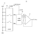
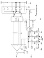
도 1은 종래기술의 일예에 의한 디지털아날로그변환기를 나타낸 도면으로서, 계조전압생성부(11)와 디코더(13), 스위치제어부(15) 및 증폭기(17)로 이루어져 있다. 1 is a diagram illustrating a digital analog converter according to an example of the prior art, and includes a
상기 계조전압생성부(11)는 복수의 저항들이 직렬로 연결되어 있어 각 저항에 걸리는 전압을 통해 서로 다른 계조전압을 생성하게 되며, 디코더(13)는 k비트 의 병렬 입력신호 중 상위 n비트의 신호를 입력받고 입력된 n비트에 해당되는 스위치를 선택하여 계조전압생성부(11)의 해당 계조전압을 제1 기준라인(VREFL)을 통해 출력하게 된다. 이때, 디코더(13)는 선택된 계조전압과 이웃하는 인접 계조전압도 선택하여 제2 기준라인(VREFH)을 통해 출력하게 된다.The gradation
스위치제어부(15)는 k비트의 병렬 입력신호 중 하위 m비트의 신호를 입력받고 m비트의 입력 데이터에 따라 복수의 내부스위치(미 도시함)를 제어하여 상기 제1 및 제2 기준라인(VREFL, VREFH)과 2m개의 출력라인을 상호 연결하고, 상기 제1 및 제2 기준라인(VREFL, VREFH)을 통해 입력된 신호를 멀티플렉싱하여 각 출력라인(2m개)으로 출력하도록 구성되어 있고, 증폭기(17)는 스위치제어부(15)를 통해 출력된 신호를 제공받아 보간을 실시하여 증폭한 후 최종 출력단으로 출력하게 된다. The
이와 같이 구성된 종래의 디지털아날로그변환기에서는 고계조를 표현하기 위해서는 계조전압생성부(11)의 저항이 디코더(13)로 입력되는 디지털데이터의 비트수를 승산한 2n(n은 비트수)개가 필요하며, 생성된 계조전압을 선택하기 위한 디코더의 스위치가 필요하다. 따라서, n비트의 해상도의 향상을 가져오려면 회로면적은 기하급수적(2n)으로 증가됨과 아울러 계조를 표현하는 동작 기준전압이 상당히 크고 정밀해야 하는 문제점이 있었다. In the conventional digital analog converter configured as described above, 2 n (n is the number of bits) in which the resistance of the
이러한 문제점을 극복하기 위하여 종래에는 2단의 디코더와 각각의 저항렬을 사용하여 디지털아날로그변환기를 구현하였는데, 이를 나타낸 것이 도 2이다. In order to overcome this problem, conventionally, a digital analog converter is implemented by using a two-stage decoder and a resistor row, which is illustrated in FIG. 2.
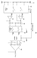
도 2는 종래의 다른 예에 의한 디지털아날로그변환기를 나타낸 도면으로서, 제1 계조전압생성부(51)와 제1 디코더(52), 버퍼(53, 54), 제2 계조전압생성부(55), 제2 디코더(56), 스위치제어부(57) 및 증폭기(58)로 이루어져 있다. 2 is a diagram illustrating a digital analog converter according to another conventional example, and includes a first
상기 제1 계조전압생성부(51)는 복수의 저항들이 직렬로 연결되어 있어 각 저항에 걸리는 전압을 통해 서로 다른 계조전압을 생성하게 되며, 제1 디코더(52)는 k비트의 병렬 입력신호 중 상위 n비트의 신호를 입력받고 입력된 n비트에 해당되는 스위치를 선택하여 제1 계조전압생성부(51)의 해당 계조전압을 제1 기준라인(V'REFL)을 통해 출력하게 된다. 이때, 제1 디코더(52)는 선택된 계조전압과 이웃하는 인접 계조전압도 선택하여 제2 기준라인(V'REFH)을 통해 출력하게 된다.Since the plurality of resistors are connected in series, the first
버퍼(53, 54)는 상기 제1 및 제2 기준라인(V'REFL, V'REFH)을 통해 출력되는 신호를 증폭하여 안정화시킨 후 제2 계조전압생성부(55)로 출력하게 된다.The
제2 디코더(56)는 k비트의 병렬 입력신호 중 하위 m비트의 신호를 입력받고 입력된 m비트에 해당되는 스위치와 그와 이웃하는 인접 스위치를 각기 선택하여 제2 계조전압생성부(55)의 해당 계조전압을 제3 및 제4 기준라인(V''REFL, V''REFH)을 통해 각기 출력하게 된다.The
스위치제어부(57)는 k비트의 병렬 입력신호 중 최하위 j비트의 신호를 입력받고 입력된 j비트 데이터에 따라 복수의 내부스위치(미 도시함)를 제어하여 상기 제3 및 제4 기준라인(V''REFL, V''REFH)과 복수의 출력라인(2j개)을 상호 연결하고, 상기 제3 및 제4 기준라인(V''REFL, V''REFH)을 통해 입력된 신호를 멀티플렉싱하여 각 출력라인(2j개)으로 출력하도록 구성되어 있고, 증폭기(58)는 스위치제어부(57)를 통해 출력된 신호를 제공받아 보간(Interpolation)을 실시하여 증폭한 후 소정의 계조전압을 최종 출력단(VOUT)으로 출력하게 된다. The
도 2에서 제1 및 제2 디코더(52, 56)는 인가된 전압을 분배(divide)하기 위한 저항렬과, 상기 저항렬에 의해 출력된 전압 중 디지털데이터에 대응하는 아날로그 전압을 출력하기 위한 스위치를 각각 구비한다. In FIG. 2, the first and
그리고, 제1 디코더(52)와 제2 디코더(56)는 버퍼(53, 54)에 의해 상호 연결되는데, 이는 제2 계조전압생성부(55)의 저항렬에 의해 제1 디코더(52)에서 분배된 전압레벨이 영향을 받지 않도록 하기 위한 것이다.In addition, the
즉, 도 2는 n비트와 m비트의 제1 및 제2 디코더(52, 56)를 통해 출력된 아날로그 값을 스위치제어부(57)로 인가하고, j비트 증폭기(58)의 보간 동작에 의해 최종적인 아날로그 계조전압을 최종 출력단(VOUT)을 통해 외부에 전달하게 된다.That is, FIG. 2 applies an analog value output through the first and
이와 같이 구성된 종래의 디지털아날로그변환기(50)는 채널당 2개의 버퍼(53, 54)가 추가로 들어가게 되어 회로면적이 증가되게 된다.In the conventional digital
또한, 버퍼(53, 54)를 이용하여 구현된 디지털아날로그변환기(50)는 버퍼(53, 54)가 갖는 오프셋전압 때문에, 버퍼의 오프셋전압 이상의 정확도를 갖는 고계조의 디지털아날로그변환기를 설계하는데 제약이 따르게 된다.In addition, the digital
이와 같은 종래기술은 처리해야 할 데이터의 비트 수가 늘어나면 날수록 계조전압생성부(51, 55)의 저항 개수와 디코더(52, 56)의 개수가 증가하게 되므로 디지털아날로그변환기의 사이즈가 기하급수적으로 커지게 된다. 일반적으로 상기 도 1 및 도 2와 같은 방식은 n비트가 증가될 때 2n만큼 사이즈가 증가하게 된다. In the conventional art, as the number of bits of data to be processed increases, the number of resistors of the
도 2의 경우에는 디코더를 n비트와 m비트를 나누어 데이터를 처리하였기 때문에 도 1에 비해서는 사이즈를 줄일 수 있었으나, 이 또한 추가적인 저항에 의한 전압분배 방식이 필요하고, 출력전압의 에러를 줄이기 위해 추가적인 버퍼가 필요하게 됨에 따라 디코더에서 줄어든 사이즈만큼 다시 커져서 사이즈를 줄인 이점이 없어지게 되는 것이다.In the case of FIG. 2, since the decoder processes data by dividing n bits and m bits, the size can be reduced compared to FIG. 1, but this also requires a voltage division method by an additional resistor, and in order to reduce an error in the output voltage. As additional buffers are needed, the size of the decoder is increased by the reduced size, so there is no advantage in reducing the size.
본 발명의 목적은 디지털아날로그변환기로 입력되는 디지털데이터를 비트별로 분리하여 처리하되 전압분배 방식과 전류조절 방식을 혼합하여 계조를 표현함으로써, 비트 수의 증가에 따라 기하급수적으로 증가되는 사이즈를 효율적으로 줄일 수 있음과 아울러 높은 해상도를 확보할 수 있는 디지털 디스플레이의 디지털 아날로그 변환장치를 제공하는 데 있다. An object of the present invention is to process the digital data input to the digital analog converter by bit, but expressing the gray scale by mixing the voltage distribution method and the current control method, efficiently increasing the size exponentially with the increase in the number of bits The present invention provides a digital-to-analog converter for a digital display that can be reduced and ensure high resolution.
본 발명의 다른 목적은 디지털아날로그변환기를 전압분배 방식과 전류조절 방식을 혼합하여 계조를 표현하되 디지털아날로그변환기를 선형으로 설계함으로써, 각 픽셀의 광투과율 특성에 따라 각 픽셀의 계조전압을 최적으로 조절하는 것이 가능한 디지털 디스플레이의 디지털 아날로그 변환장치를 제공하는 데 있다. Another object of the present invention is to express the gray scale by mixing the voltage distribution method and the current control method of the digital analog converter, but by designing the digital analog converter linearly, the gray voltage of each pixel is optimally adjusted according to the light transmittance characteristics of each pixel. It is to provide a digital analog converter of a digital display that can be.
상기 목적을 달성하기 위한 본 발명의 기술적 수단은, 복수의 저항이 직렬로 연결되어 각 저항에 걸리는 전압을 통해 서로 다른 계조전압을 생성하는 계조전압생성부; k비트의 병렬 입력데이터 중 상위 n비트에 대한 데이터를 입력받고 입력된 n비트에 해당되는 한 쌍의 스위치를 선택하여 계조전압생성부의 해당 계조전압을 제1 및 제2 기준라인을 통해 출력하는 디코더; 상기 k비트의 병렬 입력데이터 중 하위 m비트의 입력 데이터에 따라 복수의 내부스위치를 제어하여 상기 제1 및 제2 기준라인과 복수의 출력라인을 상호 연결하고, 상기 제1 및 제2 기준라인으로 입력된 데이터를 복수의 출력라인을 통해 출력하는 스위치제어부; 상기 스위치제어부를 통해 출력된 신호를 복수의 입력라인을 통해 제공받아 증폭한 후 소정의 계조전압을 출력하는 증폭기; 및 상기 k비트의 병렬 입력데이터 중 최하위 j비트의 입력데이터에 따라 작동되되, 상기 증폭기의 출력을 상기 입력데이터에 대응하여 미리 설정된 전류량만큼 접지전압으로 인가하여 증폭기의 계조전압을 조절하는 전류디코더;를 포함하는 것을 특징으로 한다. Technical means of the present invention for achieving the above object is, a plurality of resistors are connected in series to generate a different gray voltage through the voltage applied to each resistor; Decoder that receives data for upper n bits among parallel input data of k bits and selects a pair of switches corresponding to the input n bits and outputs the corresponding gray voltages of the gray voltage generator through the first and second reference lines ; A plurality of internal switches are controlled according to the lower m bits of input data of the k bits of parallel input data to interconnect the first and second reference lines and the plurality of output lines, and to the first and second reference lines. A switch controller for outputting input data through a plurality of output lines; An amplifier for amplifying the signal output through the switch control unit through a plurality of input lines and outputting a predetermined gray scale voltage; And a current decoder operated according to input data of the lowest j bits of the parallel input data of k bits, and controlling the gray voltage of the amplifier by applying the output of the amplifier to a ground voltage by a preset amount of current corresponding to the input data. Characterized in that it comprises a.
상기 전류디코더는, 증폭기의 출력단에서 반전입력단자로 피드백되는 전류통로에 설치된 피드백 저항; 상기 피드백 저항에 병렬로 연결된 스위칭소자; 및 상기 피드백 저항의 일측과 접지전압단 사이에 직렬 연결되되 최하위 비트의 입력 데이터에 따라 스위칭되어 미리 설정된 일정 전류를 접지전압 측으로 흘리는 정전류부;를 포함하여 구성된 것을 특징으로 한다.The current decoder may include: a feedback resistor installed in a current path fed back from the output terminal of the amplifier to the inverting input terminal; A switching element connected in parallel with the feedback resistor; And a constant current unit connected in series between one side of the feedback resistor and the ground voltage terminal and switched according to input data of the least significant bit to flow a predetermined current to the ground voltage side.
상기 정전류부는 최하위 비트의 비트 수에 대응되는 개수로 설치되되, 정전류부가 복수 개일 경우 피드백 저항의 일측과 접지전압단 사이에서 상호 병렬로 설치되는 것을 특징으로 하며, 상기 복수의 정전류부는 최하위 j비트 중 서로 다른 비트데이터를 각기 입력받아 작동하고, 상기 복수의 정전류부는 입력되는 비트 데이터에 따라 IREF×2p(단, p는 입력비트의 10진 자리값임)의 전류량을 접지전압으로 인가하는 것을 특징으로 한다.The constant current unit is installed in a number corresponding to the number of bits of the least significant bit, when there are a plurality of constant current unit is characterized in that they are installed in parallel between one side of the feedback resistor and the ground voltage terminal, wherein the plurality of constant current unit of the lowest j bits It operates by receiving different bit data respectively, and the plurality of constant current unit applies the current amount of I REF × 2 p (where p is the decimal place value of the input bit) as the ground voltage according to the input bit data. It is done.
상기 정전류부는, 상기 피드백 저항의 일측과 정전류원 사이의 전류통로에 직렬 연결되어 최하위 비트 중 특정 비트의 데이터를 입력받아 스위칭되는 스위칭수단; 및 상기 스위칭수단의 일측과 접지전압단 사이에 직렬 연결되어 스위칭수단의 도통에 따라 증폭기에서 출력되는 일정 전류를 접지전압으로 인가하는 정전류원;을 포함하여 구성된 것을 특징으로 한다. The constant current unit may include: switching means connected in series with a current path between one side of the feedback resistor and a constant current source and receiving data of a specific bit among the least significant bits; And a constant current source connected in series between one side of the switching means and the ground voltage terminal to apply a constant current output from the amplifier as the ground voltage according to the conduction of the switching means.
상기 목적을 달성하기 위한 본 발명의 다른 기술적 수단은, 복수의 저항이 직렬로 연결되어 각 저항에 걸리는 전압을 통해 서로 다른 계조전압을 생성하는 계조전압생성부; k비트의 병렬 입력데이터 중 상위 n비트에 대한 데이터를 입력받고 입력된 n비트에 해당되는 한 쌍의 스위치를 선택하여 계조전압생성부의 해당 계조전압을 제1 및 제2 기준라인을 통해 출력하는 디코더; 상기 k비트의 병렬 입력데이 터 중 하위 m비트의 입력 데이터에 따라 복수의 내부스위치를 제어하여 상기 제1 및 제2 기준라인과 복수의 출력라인을 상호 연결하고, 상기 제1 및 제2 기준라인으로 입력된 데이터를 복수의 출력라인을 통해 출력하는 스위치제어부; 상기 스위치제어부를 통해 출력된 신호를 복수의 입력라인을 통해 제공받아 증폭한 후 소정의 계조전압을 출력하는 증폭기; 및 상기 k비트의 병렬 입력데이터 중 최하위 j비트의 입력데이터에 따라 작동되되, 전원전압을 상기 입력데이터에 대응하여 미리 설정된 전류량만큼 증폭기의 출력단으로 인가하여 증폭기의 계조전압을 조절하는 전류디코더;를 포함하는 것을 특징으로 한다.Another technical means of achieving the above object is a gradation voltage generation unit for generating a different gradation voltage through the voltage applied to each resistor in series with a plurality of resistors; Decoder that receives data for upper n bits among parallel input data of k bits and selects a pair of switches corresponding to the input n bits and outputs the corresponding gray voltages of the gray voltage generator through the first and second reference lines ; A plurality of internal switches are controlled according to the lower m bits of input data of the k bits of parallel input data to interconnect the first and second reference lines and the plurality of output lines, and the first and second reference lines are connected to each other. A switch controller for outputting data input through the plurality of output lines; An amplifier for amplifying the signal output through the switch control unit through a plurality of input lines and outputting a predetermined gray scale voltage; And a current decoder operated according to the lowest j bits of input data of the k-bit parallel input data, and applying a power supply voltage to the output terminal of the amplifier according to the input data to adjust the gray voltage of the amplifier. It is characterized by including.
상기 전류디코더는, 증폭기의 출력단에서 반전입력단자로 피드백되는 전류통로에 설치된 피드백 저항; 상기 피드백 저항에 병렬로 연결된 스위칭소자; 및 상기 피드백 저항의 일측과 전원전압단 사이에 직렬 연결되되 최하위 비트의 입력 데이터에 따라 스위칭되어 미리 설정된 일정 전류를 증폭기의 출력단으로 인가하는 정전류부;를 포함하여 구성된 것을 특징으로 한다.The current decoder may include: a feedback resistor installed in a current path fed back from the output terminal of the amplifier to the inverting input terminal; A switching element connected in parallel with the feedback resistor; And a constant current unit connected in series between one side of the feedback resistor and a power supply voltage terminal and switched according to input data of a least significant bit to apply a predetermined constant current to an output terminal of the amplifier.
상기 정전류부는 최하위 비트의 비트 수에 대응되는 개수로 설치되되, 정전류부가 복수 개일 경우 피드백 저항의 일측과 전원전압단 사이에서 상호 병렬로 설치되며, 상기 복수의 정전류부는 최하위 j비트 중 서로 다른 비트데이터를 각기 입력받아 작동하고, 상기 복수의 정전류부는 입력되는 비트 데이터에 따라 IREF×2p(단, p는 입력비트의 10진 자리값임)의 전류량을 증폭기의 출력단으로 인가하는 것을 특징으로 한다.The constant current unit is installed in a number corresponding to the number of bits of the least significant bit, and when there are a plurality of constant current units, they are installed in parallel between one side of the feedback resistor and the power supply voltage terminal, and the plurality of constant current units have different bit data among the lowest j bits. Each of the plurality of constant current units is configured to apply an amount of current of I REF × 2 p (where p is a decimal place value of the input bit) to the output terminal of the amplifier according to the input bit data.
상기 정전류부는, 상기 피드백 저항의 일측과 정전류원 사이의 전류통로에 직렬 연결되어 최하위 비트 중 특정 비트의 데이터를 입력받아 스위칭되는 스위칭수단; 및 상기 스위칭수단의 일측과 전원전압단 사이에 직렬 연결되어 스위칭수단의 도통에 따라 전원전압을 피드백 저항을 통해 증폭기의 출력단으로 인가하는 정전류원;을 포함하여 구성된 것을 특징으로 한다.The constant current unit may include: switching means connected in series with a current path between one side of the feedback resistor and a constant current source and receiving data of a specific bit among the least significant bits; And a constant current source connected in series between one side of the switching means and the power supply voltage terminal to apply the power supply voltage to the output terminal of the amplifier through a feedback resistor in accordance with the conduction of the switching means.
이상에서 설명한 바와 같이 본 발명은 입력 디지털데이터에 대한 비트 수의 증가에 따라 기하급수적으로 증가되는 사이즈를 보다 효율적으로 줄일 수 있음과 아울러 전압분배와 전류조절 방식을 이용하여 고계조의 표현이 용이해짐에 따라 높은 해상도를 확보할 수 있는 이점이 있다.As described above, the present invention can more efficiently reduce the size that increases exponentially with the increase in the number of bits for the input digital data, and facilitate the expression of high gradation by using the voltage distribution and current control schemes. As a result, it is possible to secure a high resolution.
또한, 디지털아날로그변환기를 선형으로 설계하여 각 픽셀의 광투과율 특성에 따라 각 픽셀의 계조전압을 최적으로 조절하는 것이 가능함으로써, 디스플레이의 색감을 자연색에 가깝게 표현하여 고품위의 영상을 제공하는 것이 가능하고, 이에 따라 시장경쟁력을 향상시킬 수 있는 이점이 있다.In addition, by designing a digital analog converter linearly, it is possible to optimally adjust the gradation voltage of each pixel according to the light transmittance characteristics of each pixel, thereby providing a high quality image by expressing the color of the display close to natural colors. Therefore, there is an advantage that can improve market competitiveness.
이하, 첨부된 도면을 참조하여 본 발명의 실시예에 대하여 보다 상세하게 설명하고자 한다.Hereinafter, embodiments of the present invention will be described in detail with reference to the accompanying drawings.
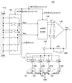
도 3은 본 발명의 일실시예에 의한 디지털 디스플레이의 디지털아날로그변환 기를 나타낸 회로블록도로서, 계조전압생성부(110)와 디코더(120), 스위치제어부(130), 증폭기(140) 및 전류디코더(150)로 이루어져 있다. 3 is a circuit block diagram illustrating a digital analog converter of a digital display according to an embodiment of the present invention, wherein a
상기 계조전압생성부(110)는 복수의 저항들이 직렬로 연결되어 있어 각 저항에 걸리는 전압을 통해 서로 다른 계조전압을 생성하게 된다.The
디코더(120)는 k비트(n+m+j비트)의 병렬 입력데이터(D<j+m+n:1>) 중 상위 n비트에 대한 데이터(D<j+m+n:j+m+1>)>를 입력받고 입력된 n비트에 해당되는 한 쌍의 스위치를 선택하여 계조전압생성부(110)의 해당 계조전압을 제1 및 제2 기준라인(VREFL, VREFH)을 통해 출력하도록 구성되어 있다. The
스위치제어부(130)는 k비트의 병렬 입력 데이터 중 하위 m비트의 입력 데이터(D<j+m:j+1>)에 따라 복수의 내부 스위치(미 도시함)를 제어하여 상기 제1 및 제2 기준라인(VREFL, VREFH)과 복수의 출력라인(2m개)을 상호 연결하고, 상기 제1 및 제2 기준라인(VREFL, VREFH)을 통해 입력된 신호를 멀티플렉싱하여 각 출력라인(2m개)을 통해 출력하도록 구성되어 있다. The
증폭기(140)는 상기 스위치제어부(130)를 통해 출력된 복수의 입력신호를 제공받아 보간(interpolation)을 실시하여 증폭한 후 액정패널의 해당 셀로 출력하도록 구성되어 있다.The
전류디코더(150)는 상기 k비트의 병렬 입력데이터 중 최하위 j비트의 입력 데이터(D<j:1>)에 따라 작동되어 상기 증폭기(140)를 통해 출력되는 전류를 피드백 루프를 통해 미리 설정된 전류량만큼 접지전압단(VSS)으로 인가하도록 구성되어 있다. The
또한, 상기 전류디코더(150)는 피드백 저항(FR1)과 스위칭소자(SW1) 및 정전류부(151)를 포함하여 구성되어 있다.In addition, the
상기 피드백 저항(FR1)은 증폭기(140)의 출력단(VOUT)에서 증폭기(140)의 반전입력단자(-)로 피드백되는 전류통로에 설치되어 있고, 스위칭소자(SW1)는 피드백 저항(FR1)에 병렬로 연결되어 있다. The feedback resistor FR1 is provided in a current path fed back from the output terminal V OUT of the
정전류부(151)는 피드백 저항(FR1)의 일측과 접지전압단(VSS) 사이에 직렬 연결되되 최하위 비트의 입력 데이터에 따라 스위칭되어 미리 설정된 일정 전류를 접지전압(VSS) 측으로 흘리도록 구성되어 있다.The constant
상기 정전류부(151)는 최하위 비트의 비트 수에 대응되는 개수로 설치되는 것이 바람직한 데, 예컨대 최하위 비트가 1비트일 경우에는 정전류부가 1개(151)로 구성되며, 최하위 비트가 2비트일 경우에는 정전류부가 2개(151, 152)로 구성되고, 최하위 비트가 3비트일 경우에는 정전류부가 3개(151, 152, 153)로 구성되는 것이 바람직하다. The constant
아울러, 정전류부(151)가 복수 개(151∼155)일 경우 피드백 저항(FR1)의 일측과 접지전압단(VSS) 사이에서 상호 병렬로 설치되어 서로 다른 비트의 데이터를 입력받아 작동하게 된다. 이때, 각 정전류부(151∼155)는 전류량이 서로 상이하게 설정되어 있다.In addition, when there are a plurality of constant
아울러, 상기 각 정전류부(151∼155)는 스위칭수단(NM)과 정전류원(CCS)을 포함하여 구성되어 있는 데, 상기 스위칭수단(NM)은 피드백 저항(FR1)의 일측과 정전류원(CCS) 사이의 전류통로에 직렬 연결되어 최하위 비트 중 특정 비트를 입력 데이터로 하여 스위칭되도록 구성되어 있고, 정전류원(CCS)은 스위칭수단(NM)의 일측과 접지전압단(VSS) 사이에 직렬 연결되어 스위칭수단(NM)의 도통에 따라 증폭기(140)에서 출력되는 일정 전류를 접지전압(VSS)으로 인가하도록 구성되어 있다.In addition, each of the constant
상기에서 각 정전류부(151∼155)의 스위칭수단(NM)은 최하위 j비트 중 특정 비트의 디지털데이터를 입력으로 하여 스위칭되는 데, 여기서 스위칭수단(NM)은 N모스 트랜지스터이다.The switching means NM of each of the constant
상기 정전류부(151)가 복수 개(151∼155)일 경우, 각 정전류부(151∼155)의 정전류원(CCS)은 해당 스위칭수단(NM)으로 입력되는 각 비트 데이터에 따라 IREF×2p(단, p는 입력비트의 10진 자리값임)의 전류량을 접지전압단(VSS)으로 인가하게 된다.When there are a plurality of constant
상기에서 피드백 저항(FR1)에 병렬로 설치된 스위칭소자(SW1)는 최하위 j비트의 디지털데이터가 모두 '0'일 경우에 턴온되도록 구성되어 있다.The switching device SW1 disposed in parallel to the feedback resistor FR1 is configured to be turned on when all of the lowest j bits of digital data are '0'.
이와 같이 구성된 디지털아날로그변환기(100)는 k비트로 이루어진 입력 디지털데이터를 상위비트(n비트)와 하위비트(m비트) 및 최하위비트(j비트)로 각각 나누고, 상기 상위비트(n비트)와 하위비트(m비트) 및 최하위비트(j비트)를 상호 직렬 연결된 다단의 아날로그변환수단(120, 130, 150)을 통해 아날로그 신호로 각각 변 환하되, 상기 상위비트(n비트)와 하위비트(m비트)는 전압분배 방식을 통해 아날로그 신호로 변환되고, 최하위비트(j비트)는 전류제어 방식을 통해 아날로그 신호로 변환되어 픽셀의 계조전압을 표현하게 된다.The
즉, k비트의 디지털데이터를 상위 n비트와 하위 m비트 및 최하위 j비트로 각각 나누고, 각 비트에 해당되는 디지털데이터를 디코더(120)와 스위치제어부(130) 및 전류디코더(150)로 각기 입력함에 따라 디지털아날로그변환기의 사이즈를 축소하고 해상도를 향상시키고자 한 것이다.That is, the k-bit digital data is divided into upper n bits, lower m bits, and lowest j bits, respectively, and digital data corresponding to each bit is input to the
이와 같이 구성된 디지털아날로그변환기(100)에서 k비트의 병렬 입력 데이터 중 상위 n비트의 데이터가 디코더(120)로 입력되면, 디코더(120)는 입력된 n비트에 해당되는 스위치를 선택하여 계조전압생성부(110)의 해당 계조전압을 제1 기준라인(VREFL)을 통해 출력하게 되는 데, 이때 디코더(120)는 선택된 계조전압과 이웃하는 인접 계조전압도 선택하여 제2 기준라인(VREFH)을 통해 출력하게 된다. When the high-order n bits of the k-bit parallel input data are input to the
상기에서 해당 계조전압과 그에 이웃하는 인접 계조전압에 대한 선택은 디스플레이의 그레이 스케일 구현 방식에 따라 그 적용이 달라진다. 즉, 디스플레이가 포지티브 그레이 스케일 방식인 경우에는 특정 저항의 하단에 걸리는 전압이 입력 디지털데이터에 해당하는 계조전압으로 제1 기준라인(VREFL)으로 출력되게 되고, 상기 저항의 상단에 걸리는 전압이 계조전압에 이웃하는 인접 계조전압에 해당되어 제2 기준라인(VREFH)으로 출력되게 된다.In the above, the selection of the corresponding gradation voltage and the neighboring gradation voltages adjacent thereto is different depending on the gray scale implementation method of the display. That is, when the display is a positive gray scale type, the voltage applied to the lower end of a specific resistor is output to the first reference line V REFL as the gray voltage corresponding to the input digital data, and the voltage applied to the upper end of the resistor is grayed out. The gray level voltage adjacent to the voltage is output to the second reference line V REFH .
물론, 네거티브 그레이 스케일 방식인 경우에는 저항의 상단에 걸리는 전압 이 입력 디지털데이터에 해당하는 계조전압으로 제2 기준라인(VREFH)으로 출력되게 되고, 상기 저항의 하단에 걸리는 전압이 계조전압에 이웃하는 인접 계조전압에 해당되어 제1 기준라인(VREFL)으로 출력되게 된다.Of course, in the case of the negative gray scale method, the voltage applied to the upper end of the resistor is output to the second reference line V REFH as the gray voltage corresponding to the input digital data, and the voltage applied to the lower end of the resistor is adjacent to the gray voltage. The corresponding gray level voltage is output to the first reference line V REFL .
스위치제어부(130)는 k비트의 병렬 입력데이터 중 하위 m비트의 데이터를 입력받고 입력된 m비트의 데이터에 따라 내부 스위치들(미 도시함)을 제어하여 제1 기준라인(VREFL)과 제2 기준라인(VREFH)을 통해 입력된 하한전압과 상한전압을 멀티플렉싱하여 복수의 출력라인(2m개)을 통해 출력하게 된다.The
도 4a 및 도 4b는 스위치제어부(130)로 입력되는 디지털데이터에 따라 제1 및 제2 기준라인(VREFL, VREFH)을 통해 입력되는 하한전압과 상한전압을 복수의 출력라인과 멀티플렉싱한 예를 나타낸 것이다.4A and 4B illustrate an example of multiplexing a lower limit voltage and an upper limit voltage with a plurality of output lines through the first and second reference lines V REFL and V REFH according to digital data input to the
예컨대, 스위치제어부(130)로 입력되는 디지털데이터가 2비트이고, 그 디지털데이터가 (1, 1)일 경우 도 4a와 같이 제1 기준라인(VREFL)에서 출력되는 하한전압에 1개의 출력라인이 결합되도록 내부 스위치(미 도시함)를 제어하고, 제2 기준라인(VREFL)에서 출력되는 상한전압에 3개의 출력라인이 결합되도록 내부 스위치를 제어하게 된다.For example, when the digital data input to the
이와 같이 내부 스위치를 제어할 경우 스위치제어부(130)는 아래 수학식 1과 같은 출력을 얻을 수 있다. In this way, when controlling the internal switch, the

즉, 제1 기준라인(VREFL)을 통해 출력되는 하한전압이 2V이고 제2 기준라인(VREFH)을 통해 출력되는 상한전압이 3V일 경우, 도 4a는 상기 수학식1에 의해 ![]()
![]()
도 4b의 경우에는 스위치제어부(130)로 입력되는 디지털데이터가 2비트이고, 그 디지털데이터가 (1, 0)일 경우 하한전압에 2개의 출력라인이 결합되도록 내부 스위치를 제어하고, 상한전압에도 2개의 출력라인이 결합되도록 내부 스위치를 제어하게 된다.In the case of FIG. 4B, when the digital data input to the
만일, 하한전압이 2V이고 상한전압이 3V일 경우, 도 4b는 상기 수학식1에 의해 ![]()
![]()
물론, 입력 디지털데이터에 따른 내부 스위치들의 결합 관계는 실시예에 불과할 뿐 설계에 따라 변경될 수 있는 것이다. Of course, the coupling relationship of the internal switches according to the input digital data is only an embodiment and can be changed according to design.
이와 같이 스위치제어부(130)의 복수의 출력라인을 통해 출력된 아날로그 신호는 증폭기(140)로 입력되고, 증폭기(140)는 입력된 아날로그 신호의 보간을 실시하여 증폭한 후 최종 출력단으로 소정의 계조전압을 출력하게 된다. As described above, the analog signals output through the plurality of output lines of the
그리고, 전류디코더(150)는 k비트의 병렬 입력데이터 중 최하위 j비트의 데 이터를 입력받고 입력된 j비트에 따라 정전류부(151∼155)의 특정 스위칭수단(NM)을 선택하여 증폭기(140)를 통해 출력되는 전류 중 미리 설정된 전류를 접지전압단(VSS)으로 인가하게 된다. The
예컨대, 상기 전류디코더(150)로 입력되는 최하위 j비트가 2비트일 경우에는 정전류부를 2j개(4개)가 아니라 j개(2개; 151, 152)로 구성하게 되는 데, 이때 각 정전류부(151, 152)의 스위칭수단(NM)으로 각각 입력된 디지털데이터가 모두 0일 경우에는 제1 및 제2 정전류부(151, 152)의 스위칭수단(NM)은 모두 턴오프됨과 아울러 전류디코더(150)는 피드백 저항(FR1)에 병렬로 연결된 스위칭소자(SW1)를 턴온시키게 된다. For example, when the lowest j bit input to the
그리고, 각 정전류부(151, 152)의 스위칭수단(NM)으로 각각 입력된 디지털데이터가 0과 1일 경우에는 제1 정전류부(151)의 스위칭수단(NM)은 턴온되고 제2 정전류부(152)의 스위칭수단(NM)은 턴오프됨과 아울러 스위칭소자(SW1)는 전류디코더(150)에 의해 턴오프되며, 각 정전류부(151, 152)의 스위칭수단(NM)으로 각각 입력된 디지털데이터가 1과 0일 경우에는 제1 정전류부(151)의 스위칭수단(NM)은 턴오프되고 제2 정전류부(152)의 스위칭수단(NM)은 턴온됨과 아울러 스위칭소자(SW1)는 전류디코더(150)에 의해 턴오프되며, 각 정전류부(151, 152)의 스위칭수단(NM)으로 각각 입력된 디지털데이터가 모두 1일 경우에는 제1 및 제2 정전류부(151, 152)의 스위칭수단(NM)은 모두 턴온됨과 아울러 스위칭소자(SW1)는 전류디코더(150)에 의해 턴오프된다.When the digital data input to the switching means NM of the constant
아래 표 1에서는 전류디코더(150)로 입력되는 디지털데이터가 3비트일 경우에 제1 정전류부(151)와 제2 정전류부(152) 및 제3 정전류부(153)의 각 스위칭수단(NM)과 스위치소자(SW1)의 온오프 동작 상태를 나타낸 것이다.Table 1 below shows the switching means NM of the first constant
상기 표 1에서와 같이 디지털데이터에 따라 각 정전류부(151∼153)를 조합하여 작동시킴에 따라 정전류부의 개수를 최소화할 수 있는 데, 이는 각 정전류부(151∼153)에 설정된 정전류량이 다르기 때문에 가능하며, 해상도를 높이더라도 디지털아날로그변환기의 사이즈를 최소화할 수 있게 된다.As shown in Table 1, the number of constant current units can be minimized by combining and operating the constant
즉, 도 3은 입력된 디지털데이터(D<j:1>)에 따라 전류디코더(150)에서 결정된 전류가 증폭기(140)의 피드백 저항(FR1)을 통해 접지전압단(VSS)으로 흐르면 증폭기(140)의 출력단(VOUT)에서는 그에 따른 전압 강하가 발생되며, 전류의 양에 따라 출력단(VOUT)의 전압 강하가 달라지기 때문에 선형적으로 전압을 나누어 계조를 표현할 수 있다. That is, FIG. 3 illustrates that when the current determined by the
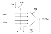
도 5는 도 3을 간략하게 나타낸 회로도로서, 전류디코더(150)로 입력되는 최하위 비트가 3비트일 경우를 예로 하여 설명하고자 한다. FIG. 5 is a circuit diagram briefly illustrating FIG. 3 and will be described by taking an example where the least significant bit input to the
스위치제어부(130)에서 출력되는 전압을 VA라고 가정하면, 증폭기(140)의 출력전압(VOUT)은 아래 수학식 2와 같다. Assuming that the voltage output from the

상기 수학식 2에서 식①의 VX에 식②를 대입하여 풀면 아래 수학식 3과 같이 나타난다.Solving by substituting Equation ② into V X of

상기 수학식 3에서 보는 바와 같이 스위치제어부(130)의 출력전압(VOUT)과 전류디코더(150)로 입력되는 디지털데이터(D<j:1>)에 따라 접지전압단(VSS)으로 흐르는 전류를 N배하여 가산함에 따라 결국 선형적으로 전압을 출력하게 된다.As shown in
전류디코더(150)로 입력되는 최하위 비트가 3비트일 경우 각 디지털데이터에 따른 증폭기(140)의 출력전압(VOUT)은 아래의 표 2와 같다. When the least significant bit input to the
아울러, 상기 표 2에서와 같이 전류디코더(150)로 입력되는 디지털데이터(D<j:1>)가 '000'일 경우에는 정전류부(151∼155)의 모든 스위칭수단(NM)이 턴오프되어 증폭기(140)의 출력전압(VOUT)이 접지전압단(VSS) 측으로 흐르지 않게 되며, 이때에는 피드백 저항(FR1)에 병렬로 연결된 스위칭소자(SW1)를 턴온시켜 증폭기(140)의 출력전압(VOUT)이 피드백 저항(FR1)에 의한 전압 손실이 없도록 하는 것이 바람직하다. In addition, as shown in Table 2, when the digital data D <j: 1> input to the
도 6은 본 발명의 다른 실시예에 의한 디지털아날로그변환기를 나타낸 회로도로서, 계조전압생성부(110)와 디코더(120), 스위치제어부(130), 증폭기(140) 및 전류디코더(160)로 이루어져 있다. 6 is a circuit diagram illustrating a digital analog converter according to another embodiment of the present invention, and includes a
도 6의 계조전압생성부(110)와 디코더(120), 스위치제어부(130) 및 증폭기(140)는 도 3의 구성과 동일하며, 전류디코더(160)의 구성이 도 3과 상이한 것이다. The
따라서, 도 3과 동일한 구성인 계조전압생성부(110)와 디코더(120), 스위치제어부(130) 및 증폭기(140)에 대해서는 구체적인 설명을 생략하도록 하겠으며, 전류디코더를 중심으로 설명하고자 한다.Therefore, a detailed description of the
즉, 전류디코더(160)는 k비트의 병렬 입력데이터 중 최하위 j비트의 입력 데이터에 따라 작동되어 전원전압을 증폭기(140)의 피드백 루프를 통해 미리 설정된 전류량만큼 증폭기(140)의 출력단(VOUT)으로 인가하도록 구성되어 있다. That is, the
상기 전류디코더(160)는 피드백 저항(FR2)과 스위칭소자(SW2) 및 정전류부(161)를 포함하여 구성되어 있다.The
상기 피드백 저항(FR2)은 증폭기(140)의 출력단(VOUT)에서 증폭기(140)의 반전입력단자(-)로 피드백되는 전류통로에 설치되어 있고, 스위칭소자(SW2)는 피드백 저항(FR2)에 병렬로 연결되어 있다. The feedback resistor FR2 is provided in a current path fed back from the output terminal V OUT of the
정전류부(161)는 피드백 저항(FR2)의 일측과 전원전압단(VDD) 사이에 직렬 연결되되 최하위 비트의 입력 데이터에 따라 스위칭되어 미리 설정된 일정 전류를 증폭기(140)의 출력단(VOUT)으로 인가하도록 구성되어 있다.The constant
상기 정전류부(161)는 최하위 비트의 비트 수에 대응되는 개수로 설치되는 것이 바람직한 데, 정전류부(161)가 복수 개(161∼165)일 경우 피드백 저항(FR2)의 일측과 전원전압단(VDD) 사이에서 상호 병렬로 설치되어 서로 다른 비트의 데이터를 입력받아 작동하게 된다.The constant
이때, 각 정전류부(161∼165)는 증폭기(140)의 출력단(VOUT)으로 인가하는 전류량이 서로 상이하도록 구성되어 있다.At this time, each of the constant
아울러, 상기 각 정전류부(161∼165)는 스위칭수단(PM)과 정전류원(CCS)을 포함하여 구성되어 있는 데, 상기 스위칭수단(PM)은 피드백 저항(FR2)의 일측과 정전류원(CCS) 사이의 전류통로에 직렬 연결되어 최하위 비트 중 특정 비트를 입력 데이터로 하여 스위칭되도록 구성되어 있고, 정전류원은 스위칭수단(PM)의 일측과 전원전압단(VDD) 사이에 직렬 연결되어 스위칭수단(PM)의 도통에 따라 일정 전류를 증폭기(140)의 출력단(VOUT)으로 인가하도록 구성되어 있다.In addition, each of the constant
상기에서 각 정전류부(161∼165)의 스위칭수단(PM)은 최하위 j비트 중 특정 비트의 디지털데이터를 입력으로 하여 스위칭되는 데, 여기서 스위칭수단(PM)은 P모스 트랜지스터이다.In the above, the switching means PM of each of the constant
상기 정전류부(161)가 복수 개(161∼165)일 경우, 각 정전류부(161∼165)의 정전류원(CCS)은 해당 스위칭수단(PM)으로 입력되는 각 비트 데이터에 따라 IREF×2p(단, p는 입력비트의 10진 자리값임)의 전류량을 증폭기(140)의 출력단(VOUT)으로 인가하게 된다.When there are a plurality of constant
상기에서 피드백 저항(FR2)에 병렬로 설치된 스위칭소자(SW2)는 최하위 j비트의 디지털데이터가 모두 '0'일 경우에 턴온되도록 구성되어 있다.The switching device SW2 provided in parallel to the feedback resistor FR2 is configured to be turned on when all of the lowest j bits of digital data are '0'.
도 7은 도 6을 간략하게 나타낸 회로도로서, 도 5와 같은 방법으로 회로를 해석할 수 있다. FIG. 7 is a circuit diagram schematically illustrating FIG. 6, and the circuit may be analyzed in the same manner as in FIG. 5.
도 7은 스위치제어부(130)의 출력전압인 VA를 기준으로, 전류디코더(160)에서 피드백 저항(FR2)을 통해 증폭기(140)의 출력단(VOUT)으로 인가되는 일정전류에 따라 증폭기(140)의 출력전압을 선형적으로 감산하는 회로로서, 아래 수학식 4 및 5와 같이 표현할 수 있다.FIG. 7 illustrates an amplifier according to a constant current applied from the

상기 수학식 4에서 식③의 VX에 식④를 대입하여 풀면 아래 수학식 5를 얻을 수 있다.Equation (4) can be obtained by substituting Equation (4) into V X of Equation (3) in Equation (4).

상기 수학식 5에서 보는 바와 같이 스위치제어부(130)의 출력전압에 전류디코더(160)로 입력되는 디지털데이터에 따라 증폭기(140)의 출력단(VOUT)으로 인가되는 전류를 N배하여 감산함에 따라 결국 선형적으로 전압을 출력하게 된다.As shown in Equation 5, the current applied to the output terminal V OUT of the
전류디코더(160)로 입력되는 최하위 비트가 3비트일 경우 각 디지털데이터에 따른 증폭기(140)의 출력전압은 아래의 표 3과 같다. When the least significant bit input to the
아울러, 상기 표 3에서와 같이 전류디코더(160)로 입력되는 디지털데이터(D<j:1>)가 '000'일 경우에는 정전류부(161∼165)의 모든 스위칭수단(PM)이 턴오프되어 전원전압이 증폭기(140)의 출력단(VOUT) 측으로 흐르지 않게 되며, 이때에는 피드백 저항(FR2)에 병렬로 연결된 스위칭소자(SW2)를 턴온시켜 증폭기(140)의 출력전압(VOUT)이 피드백 저항(FR2)에 의한 전압 손실이 없도록 하는 것이 바람직하다.In addition, as shown in Table 3 above, when the digital data D <j: 1> input to the
이와 같이, 본 발명에서는 하위 m비트에 대해서는 스위치제어부(130)에서 보간 적용하여 기존과 동일하게 계조전압을 결정하고, 최하위 j비트에 대해서는 전류디코더(160)를 이용하여 증폭기(140)에서 출력되는 출력전류를 조절함에 따라 아날로그 계조전압을 결정하는 것이다. As described above, in the present invention, the gray level voltage is determined in the same manner as before by applying interpolation in the
즉, 최하위 j비트에 대해서는 전류를 조절하여 증폭기(140)의 출력전압을 변경함에 따라 최종적으로 원하는 아날로그 값을 출력할 수 있다.That is, as the output voltage of the
이와 같이 본 발명에서는 전압분배 방식과 전류조절 방식을 혼합하여 디지털데이터를 아날로그신호로 변환함에 따라 디코더 부분의 사이즈를 줄일 수 있음과 아울러 전류조절 방식을 이용함에 따라 적은 전류량으로도 고계조를 표현하는 것이 가능하여 고해상도의 영상을 용이하게 구현할 수 있다.As described above, the present invention can reduce the size of the decoder part by converting digital data into an analog signal by mixing the voltage distribution method and the current control method, and express high gradations with a small amount of current by using the current control method. It is possible to easily implement a high resolution image.
한편, 본 발명의 실시예에서 디지털아날로그변환기를 선형으로 사용하는 것에 대해 설명하였지만, 계조전압생성부의 각 저항값을 비선형으로 설계하거나 전류디코더의 정전류를 비선형으로 설계하여 디지털아날로그변환기를 비선형으로도 사용할 수 있다.On the other hand, although the use of the digital analog converter in the embodiment of the present invention has been described as linear, the non-linear design of each resistance value of the gradation voltage generating unit or the non-linear design of the constant current of the current decoder to use the digital analog converter nonlinear Can be.
또한, 본 발명의 디지털아날로그변환기가 디지털 디스플레이에 적용되는 것으로 설명하였지만, 디스플레이 장치 뿐만 아니라 모든 디지털아날로그변환기에 적용 및 사용할 수 있음은 당연하다.In addition, although the digital analog converter of the present invention has been described as being applied to a digital display, it is natural that it can be applied to and used in all digital analog converters as well as display devices.
이러한 본 발명의 바람직한 실시예는 예시의 목적을 위해 개시된 것이고, 본 발명에 대한 통상의 지식을 가진 당업자라면 본 발명의 사상과 청구범위 내에서 다양한 수정, 변경 부가가 가능할 것이며, 이러한 수정, 변경 및 부가는 하기의 특허청구범위에 속하는 것으로 보아야 할 것이다.Such preferred embodiments of the present invention are disclosed for the purpose of illustration, and those skilled in the art having various ordinary knowledge of the present invention will be able to make various modifications, changes and additions within the spirit and claims of the present invention. Additions should be considered to be within the scope of the following claims.
도 1은 종래기술의 일예에 의한 디지털아날로그변환기를 나타낸 도면이다.1 is a view showing a digital analog converter according to an example of the prior art.
도 2는 종래기술의 다른 예에 의한 디지털아날로그변환기를 나타낸 도면이다.2 is a view showing a digital analog converter according to another example of the prior art.
도 3은 본 발명의 일실시예에 의한 디지털 디스플레이의 디지털아날로그변환기를 나타낸 회로블록도이다.3 is a circuit block diagram illustrating a digital analog converter of a digital display according to an embodiment of the present invention.
도 4a 및 도 4b는 본 발명에 적용된 스위치제어부의 입력과 출력라인의 멀티플렉싱의 예를 나타낸 도면이다.4A and 4B illustrate an example of multiplexing input and output lines of a switch control unit according to the present invention.
도 5는 도 3의 디지털아날로그변환기를 간략하게 나타낸 회로도이다.FIG. 5 is a circuit diagram schematically illustrating the digital analog converter of FIG. 3.
도 6은 본 발명의 다른 실시예에 의한 디지털 디스플레이의 디지털아날로그변환기를 나타낸 회로블록도이다.6 is a circuit block diagram illustrating a digital analog converter of a digital display according to another embodiment of the present invention.
도 7은 도 6의 디지털아날로그변환기를 간략하게 나타낸 회로도이다.FIG. 7 is a circuit diagram schematically illustrating the digital analog converter of FIG. 6.
* 도면의 주요 부분에 대한 부호의 설명DESCRIPTION OF THE REFERENCE NUMERALS
100: 디지털아날로그변환기 110: 계조전압생성부100: digital analog converter 110: gray voltage generator
120: 디코더 130: 스위치제어부120: decoder 130: switch control unit
140: 증폭기 150,160: 전류디코더140:
151∼155: 정전류부 FR1,FR2: 피드백 저항151 to 155: constant current sections FR1 and FR2: feedback resistors
SW1,SW2: 스위칭소자 NM,PM: 스위칭수단SW1, SW2: switching element NM, PM: switching means
CCS: 정전류원 VREFL,VREFH: 제1 및 제2 기준라인CCS: constant current source V REFL , V REFH : first and second reference lines
Claims (16)
Priority Applications (2)
| Application Number | Priority Date | Filing Date | Title |
|---|---|---|---|
| KR1020070079594A KR101361275B1 (en) | 2007-08-08 | 2007-08-08 | Digital-analog converter of digital display device |
| US12/222,379 US8344978B2 (en) | 2007-08-08 | 2008-08-07 | Digital-to-analog converter for display device |
Applications Claiming Priority (1)
| Application Number | Priority Date | Filing Date | Title |
|---|---|---|---|
| KR1020070079594A KR101361275B1 (en) | 2007-08-08 | 2007-08-08 | Digital-analog converter of digital display device |
Publications (2)
| Publication Number | Publication Date |
|---|---|
| KR20090015344A KR20090015344A (en) | 2009-02-12 |
| KR101361275B1 true KR101361275B1 (en) | 2014-02-11 |
Family
ID=40362610
Family Applications (1)
| Application Number | Title | Priority Date | Filing Date |
|---|---|---|---|
| KR1020070079594A KR101361275B1 (en) | 2007-08-08 | 2007-08-08 | Digital-analog converter of digital display device |
Country Status (2)
| Country | Link |
|---|---|
| US (1) | US8344978B2 (en) |
| KR (1) | KR101361275B1 (en) |
Families Citing this family (12)
| Publication number | Priority date | Publication date | Assignee | Title |
|---|---|---|---|---|
| TWI386908B (en) * | 2008-10-22 | 2013-02-21 | Au Optronics Corp | Gamma voltage conversion device |
| KR101534150B1 (en) * | 2009-02-13 | 2015-07-07 | 삼성전자주식회사 | Hybrid Digital to analog converter, source driver and liquid crystal display apparatus |
| TW201503101A (en) * | 2013-07-03 | 2015-01-16 | Integrated Solutions Technology Inc | Gamma reference voltages generating circuit with output offset and display apparatus |
| CN104821828B (en) * | 2015-04-24 | 2018-07-06 | 北京大学深圳研究生院 | Low pressure digital analogue signal conversion circuit, data drive circuit and display system |
| KR20170036176A (en) * | 2015-09-23 | 2017-04-03 | 삼성디스플레이 주식회사 | Display panel driving apparatus, method of driving display panel using the display panel driving apparatus and display apparatus having the display panel driving apparatus |
| FR3047380B1 (en) * | 2016-01-29 | 2018-05-18 | STMicroelectronics (Alps) SAS | DETECTION OF AN ANALOG CONNECTION IN A VIDEO DECODER |
| JP2017183658A (en) * | 2016-03-31 | 2017-10-05 | ソニー株式会社 | Solid state image pick-up device, imaging apparatus, and electronic apparatus |
| CN107038988B (en) * | 2017-06-19 | 2019-11-05 | 京东方科技集团股份有限公司 | Control circuit, display screen, the driving method of display screen and display device |
| KR102480630B1 (en) | 2018-03-30 | 2022-12-23 | 삼성전자주식회사 | Source driver and display driver including the same |
| KR20210006614A (en) * | 2019-07-09 | 2021-01-19 | 삼성전자주식회사 | Source driver and display device including thereof |
| KR20220012546A (en) * | 2020-07-23 | 2022-02-04 | 주식회사 엘엑스세미콘 | Display driving apparatus |
| KR20230159662A (en) * | 2022-05-11 | 2023-11-21 | 삼성디스플레이 주식회사 | Gamma voltage generator, display driver, display device and method of generating a gamma voltage |
Citations (3)
| Publication number | Priority date | Publication date | Assignee | Title |
|---|---|---|---|---|
| KR20070015827A (en) * | 2005-08-01 | 2007-02-06 | 한양대학교 산학협력단 | Data Driving Circuit and Driving Method of Organic Light Emitting Display Using the same |
| KR20070015822A (en) * | 2005-08-01 | 2007-02-06 | 한양대학교 산학협력단 | Data Driving Circuit and Driving Method of Light Emitting Display Using the same |
| KR20070077047A (en) * | 2006-01-20 | 2007-07-25 | 오끼 덴끼 고오교 가부시끼가이샤 | Digital-analog converter |
Family Cites Families (14)
| Publication number | Priority date | Publication date | Assignee | Title |
|---|---|---|---|---|
| US4978959A (en) * | 1987-10-08 | 1990-12-18 | University Of Toronto Innovations Foundation | Analog to digital converter, a digital to analog converter and an operational amplifier therefor |
| US5396245A (en) * | 1993-01-21 | 1995-03-07 | Linear Technology Corporation | Digital to analog converter |
| US5859606A (en) * | 1997-07-25 | 1999-01-12 | Linear Technology Corporation | Interpolation circuit for digital-to-analog converter |
| JP3506219B2 (en) * | 1998-12-16 | 2004-03-15 | シャープ株式会社 | DA converter and liquid crystal driving device using the same |
| US6246351B1 (en) * | 1999-10-07 | 2001-06-12 | Burr-Brown Corporation | LSB interpolation circuit and method for segmented digital-to-analog converter |
| JP3281621B2 (en) * | 1999-12-21 | 2002-05-13 | 松下電器産業株式会社 | High precision DA conversion circuit |
| US6617989B2 (en) * | 2001-12-21 | 2003-09-09 | Texas Instruments Incorporated | Resistor string DAC with current source LSBs |
| US6937178B1 (en) * | 2003-05-15 | 2005-08-30 | Linear Technology Corporation | Gradient insensitive split-core digital to analog converter |
| JP2005331709A (en) * | 2004-05-20 | 2005-12-02 | Renesas Technology Corp | Liquid crystal display driving apparatus and liquid crystal display system |
| JP4472507B2 (en) * | 2004-12-16 | 2010-06-02 | 日本電気株式会社 | DIFFERENTIAL AMPLIFIER, DATA DRIVER OF DISPLAY DEVICE USING SAME, AND METHOD FOR CONTROLLING DIFFERENTIAL AMPLIFIER |
| KR100790977B1 (en) * | 2006-01-13 | 2008-01-03 | 삼성전자주식회사 | Output buffer circuit with improved output deviation and source driver circuit for flat panel display having the same |
| JP4878249B2 (en) * | 2006-09-08 | 2012-02-15 | ルネサスエレクトロニクス株式会社 | Decoder circuit, display device drive circuit and display device using the same |
| JP4401378B2 (en) * | 2006-11-02 | 2010-01-20 | Necエレクトロニクス株式会社 | DIGITAL / ANALOG CONVERSION CIRCUIT, DATA DRIVER AND DISPLAY DEVICE USING THE SAME |
| US20090033589A1 (en) * | 2007-08-01 | 2009-02-05 | Toshifumi Ozaki | Image Display Device |
-
2007
- 2007-08-08 KR KR1020070079594A patent/KR101361275B1/en active IP Right Grant
-
2008
- 2008-08-07 US US12/222,379 patent/US8344978B2/en active Active
Patent Citations (3)
| Publication number | Priority date | Publication date | Assignee | Title |
|---|---|---|---|---|
| KR20070015827A (en) * | 2005-08-01 | 2007-02-06 | 한양대학교 산학협력단 | Data Driving Circuit and Driving Method of Organic Light Emitting Display Using the same |
| KR20070015822A (en) * | 2005-08-01 | 2007-02-06 | 한양대학교 산학협력단 | Data Driving Circuit and Driving Method of Light Emitting Display Using the same |
| KR20070077047A (en) * | 2006-01-20 | 2007-07-25 | 오끼 덴끼 고오교 가부시끼가이샤 | Digital-analog converter |
Also Published As
| Publication number | Publication date |
|---|---|
| US8344978B2 (en) | 2013-01-01 |
| KR20090015344A (en) | 2009-02-12 |
| US20090046083A1 (en) | 2009-02-19 |
Similar Documents
| Publication | Publication Date | Title |
|---|---|---|
| KR101361275B1 (en) | Digital-analog converter of digital display device | |
| US7425941B2 (en) | Source driver of liquid crystal display | |
| JP3950988B2 (en) | Driving circuit for active matrix electroluminescent device | |
| KR100339807B1 (en) | Da converter and liquid crystal driving device incorporating the same | |
| US7236114B2 (en) | Digital-to-analog converters including full-type and fractional decoders, and source drivers for display panels including the same | |
| US7486303B2 (en) | Circuit for adjusting gray-scale voltages of a self-emitting display device | |
| KR100743498B1 (en) | Current driven data driver and display device having the same | |
| JP4472507B2 (en) | DIFFERENTIAL AMPLIFIER, DATA DRIVER OF DISPLAY DEVICE USING SAME, AND METHOD FOR CONTROLLING DIFFERENTIAL AMPLIFIER | |
| JP2899969B2 (en) | LCD source driver | |
| JP4661324B2 (en) | Digital analog circuit, data driver and display device | |
| JP4936854B2 (en) | Display device and display panel driver | |
| US7880692B2 (en) | Driver circuit of AMOLED with gamma correction | |
| US7423572B2 (en) | Digital-to-analog converter | |
| KR20010062324A (en) | Gray scale display reference voltage generating circuit capable of changing gamma correction characteristic and lcd drive unit employing the same | |
| KR20050076707A (en) | Light emitting elements driving circuit | |
| US11488505B2 (en) | Data driving device and gamma voltage circuit for driving pixels arranged in display | |
| JPWO2012121087A1 (en) | DIGITAL / ANALOG CONVERSION CIRCUIT AND DISPLAY DEVICE DATA DRIVER | |
| KR20170087832A (en) | Source driver for display apparatus | |
| JP5506843B2 (en) | Self-luminous display drive circuit | |
| US20070052641A1 (en) | Gray scale voltage outputting device | |
| KR20070030129A (en) | Self-luminous display device | |
| KR20070014581A (en) | Programmable gamma compensation circuit using look-up table | |
| JP2007248723A (en) | Signal voltage generation circuit, driving circuit of display apparatus, and liquid crystal display apparatus | |
| US8723587B1 (en) | Voltage generator | |
| JP2024047657A (en) | Digital-to-analog conversion circuit, data driver and display device |
Legal Events
| Date | Code | Title | Description |
|---|---|---|---|
| A201 | Request for examination | ||
| E902 | Notification of reason for refusal | ||
| E701 | Decision to grant or registration of patent right | ||
| GRNT | Written decision to grant | ||
| FPAY | Annual fee payment |
Payment date: 20161206 Year of fee payment: 4 |
|
| FPAY | Annual fee payment |
Payment date: 20171204 Year of fee payment: 5 |
|
| FPAY | Annual fee payment |
Payment date: 20181204 Year of fee payment: 6 |
|
| FPAY | Annual fee payment |
Payment date: 20191210 Year of fee payment: 7 |