EP1750304A2 - Semiconductor device - Google Patents
Semiconductor device Download PDFInfo
- Publication number
- EP1750304A2 EP1750304A2 EP06016109A EP06016109A EP1750304A2 EP 1750304 A2 EP1750304 A2 EP 1750304A2 EP 06016109 A EP06016109 A EP 06016109A EP 06016109 A EP06016109 A EP 06016109A EP 1750304 A2 EP1750304 A2 EP 1750304A2
- Authority
- EP
- European Patent Office
- Prior art keywords
- semiconductor device
- substrate
- straight line
- semiconductor
- electrical connection
- Prior art date
- Legal status (The legal status is an assumption and is not a legal conclusion. Google has not performed a legal analysis and makes no representation as to the accuracy of the status listed.)
- Withdrawn
Links
Images


Classifications
-
- H—ELECTRICITY
- H10—SEMICONDUCTOR DEVICES; ELECTRIC SOLID-STATE DEVICES NOT OTHERWISE PROVIDED FOR
- H10W—GENERIC PACKAGES, INTERCONNECTIONS, CONNECTORS OR OTHER CONSTRUCTIONAL DETAILS OF DEVICES COVERED BY CLASS H10
- H10W72/00—Interconnections or connectors in packages
- H10W72/20—Bump connectors, e.g. solder bumps or copper pillars; Dummy bumps; Thermal bumps
-
- H—ELECTRICITY
- H10—SEMICONDUCTOR DEVICES; ELECTRIC SOLID-STATE DEVICES NOT OTHERWISE PROVIDED FOR
- H10W—GENERIC PACKAGES, INTERCONNECTIONS, CONNECTORS OR OTHER CONSTRUCTIONAL DETAILS OF DEVICES COVERED BY CLASS H10
- H10W70/00—Package substrates; Interposers; Redistribution layers [RDL]
- H10W70/60—Insulating or insulated package substrates; Interposers; Redistribution layers
- H10W70/62—Insulating or insulated package substrates; Interposers; Redistribution layers characterised by their interconnections
- H10W70/65—Shapes or dispositions of interconnections
- H10W70/654—Top-view layouts
-
- H—ELECTRICITY
- H10—SEMICONDUCTOR DEVICES; ELECTRIC SOLID-STATE DEVICES NOT OTHERWISE PROVIDED FOR
- H10W—GENERIC PACKAGES, INTERCONNECTIONS, CONNECTORS OR OTHER CONSTRUCTIONAL DETAILS OF DEVICES COVERED BY CLASS H10
- H10W70/00—Package substrates; Interposers; Redistribution layers [RDL]
- H10W70/60—Insulating or insulated package substrates; Interposers; Redistribution layers
- H10W70/62—Insulating or insulated package substrates; Interposers; Redistribution layers characterised by their interconnections
- H10W70/65—Shapes or dispositions of interconnections
- H10W70/654—Top-view layouts
- H10W70/656—Fan-in layouts
-
- H—ELECTRICITY
- H10—SEMICONDUCTOR DEVICES; ELECTRIC SOLID-STATE DEVICES NOT OTHERWISE PROVIDED FOR
- H10W—GENERIC PACKAGES, INTERCONNECTIONS, CONNECTORS OR OTHER CONSTRUCTIONAL DETAILS OF DEVICES COVERED BY CLASS H10
- H10W72/00—Interconnections or connectors in packages
- H10W72/20—Bump connectors, e.g. solder bumps or copper pillars; Dummy bumps; Thermal bumps
- H10W72/251—Materials
-
- H—ELECTRICITY
- H10—SEMICONDUCTOR DEVICES; ELECTRIC SOLID-STATE DEVICES NOT OTHERWISE PROVIDED FOR
- H10W—GENERIC PACKAGES, INTERCONNECTIONS, CONNECTORS OR OTHER CONSTRUCTIONAL DETAILS OF DEVICES COVERED BY CLASS H10
- H10W72/00—Interconnections or connectors in packages
- H10W72/90—Bond pads, in general
- H10W72/921—Structures or relative sizes of bond pads
- H10W72/922—Bond pads being integral with underlying chip-level interconnections
-
- H—ELECTRICITY
- H10—SEMICONDUCTOR DEVICES; ELECTRIC SOLID-STATE DEVICES NOT OTHERWISE PROVIDED FOR
- H10W—GENERIC PACKAGES, INTERCONNECTIONS, CONNECTORS OR OTHER CONSTRUCTIONAL DETAILS OF DEVICES COVERED BY CLASS H10
- H10W72/00—Interconnections or connectors in packages
- H10W72/90—Bond pads, in general
- H10W72/921—Structures or relative sizes of bond pads
- H10W72/923—Bond pads having multiple stacked layers
-
- H—ELECTRICITY
- H10—SEMICONDUCTOR DEVICES; ELECTRIC SOLID-STATE DEVICES NOT OTHERWISE PROVIDED FOR
- H10W—GENERIC PACKAGES, INTERCONNECTIONS, CONNECTORS OR OTHER CONSTRUCTIONAL DETAILS OF DEVICES COVERED BY CLASS H10
- H10W72/00—Interconnections or connectors in packages
- H10W72/90—Bond pads, in general
- H10W72/941—Dispositions of bond pads
- H10W72/9415—Dispositions of bond pads relative to the surface, e.g. recessed, protruding
-
- H—ELECTRICITY
- H10—SEMICONDUCTOR DEVICES; ELECTRIC SOLID-STATE DEVICES NOT OTHERWISE PROVIDED FOR
- H10W—GENERIC PACKAGES, INTERCONNECTIONS, CONNECTORS OR OTHER CONSTRUCTIONAL DETAILS OF DEVICES COVERED BY CLASS H10
- H10W72/00—Interconnections or connectors in packages
- H10W72/90—Bond pads, in general
- H10W72/941—Dispositions of bond pads
- H10W72/944—Dispositions of multiple bond pads
- H10W72/9445—Top-view layouts, e.g. mirror arrays
-
- H—ELECTRICITY
- H10—SEMICONDUCTOR DEVICES; ELECTRIC SOLID-STATE DEVICES NOT OTHERWISE PROVIDED FOR
- H10W—GENERIC PACKAGES, INTERCONNECTIONS, CONNECTORS OR OTHER CONSTRUCTIONAL DETAILS OF DEVICES COVERED BY CLASS H10
- H10W72/00—Interconnections or connectors in packages
- H10W72/90—Bond pads, in general
- H10W72/951—Materials of bond pads
- H10W72/952—Materials of bond pads comprising metals or metalloids, e.g. PbSn, Ag or Cu
Definitions
- the present invention relates to a semiconductor device.
- An electronic module has been known in which a semiconductor device is mounted on an interconnect substrate (e.g. JP-A-2-272737 ).
- an interconnect substrate e.g. JP-A-2-272737 .
- it is important to electrically connect an interconnect pattern of the interconnect substrate with electrical connection sections of the semiconductor device.
- a semiconductor device comprising:
- the invention may provide a semiconductor device exhibiting excellent mounting capability.
- FIGS. 1 to 3 are views illustrative of a semiconductor device according to an embodiment to which the invention is applied.
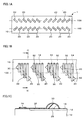
- FIG. 1A is a top view of a semiconductor device 1 according to an embodiment to which the invention is applied.
- an electrode 14 and an electrical connection section 30 are omitted for convenience of illustration.
- FIG. 1B is a partially enlarged view of FIG 1A
- FIG. 1C is a cross-sectional view along the line IC-IC in FIG. 1B.
- the semiconductor device includes a semiconductor substrate 10.
- the semiconductor substrate 10 may be a silicon substrate, for example.
- the semiconductor substrate 10 may be in the shape of a chip, as shown in FIG 1A.
- the semiconductor substrate 10 may be a semiconductor chip.
- the semiconductor substrate 10 may be in the shape of a wafer (not shown).
- the semiconductor substrate 10 may include regions in which semiconductor chips (semiconductor devices) are respectively formed.
- An integrated circuit 12 may be formed on the semiconductor substrate 10 (see FIG. 1C).
- the configuration of the integrated circuit 12 is not particularly limited.
- the integrated circuit 12 may include an active element such as a transistor and a passive element such as a resistor, coil, or capacitor.
- the surface (active surface) of the semiconductor substrate 10 on which the integrated circuit 12 is formed may be rectangular (see FIG. 1A).
- the active surface of the semiconductor substrate 10 may be square (not shown).
- a plurality of electrodes 14 are formed on the semiconductor substrate 10.
- the electrode 14 may be formed on the surface (active surface) of the semiconductor substrate 10 on which the integrated circuit 12 is formed, for example.
- the electrodes 14 may be arranged along one side of the semiconductor substrate 10.
- the electrodes 14 may be arranged along a plurality of sides of the semiconductor substrate 10. When the active surface of the semiconductor substrate 10 is rectangular, the electrodes 14 may be arranged on (only) two long sides of the active surface.
- the semiconductor device may also include electrodes arranged along the short side of the active surface of the semiconductor substrate 10 (not shown).
- the electrodes 14 may be arranged in one row along one side of the semiconductor substrate 10.
- the electrodes 14 may be arranged in a plurality of rows along one side of the semiconductor substrate 10 (not shown).
- the electrode 14 may be electrically connected with the integrated circuit 12.
- a conductor which is not electrically connected with the integrated circuit 12 may also be referred to as the electrode 14.
- the electrode 14 may be part of an internal interconnect (electrode) of the semiconductor substrate.
- the electrode 14 may be formed of a metal such as aluminum or copper.
- the semiconductor substrate 10 may include a passivation film 16.
- the passivation film 16 may be formed to expose the electrode 14.
- the passivation film 16 may have an opening which exposes the electrode 14.
- the passivation film may be an inorganic insulating film formed of SiO 2 , SiN, or the like.
- the passivation film 16 may be an organic insulating film formed of a polyimide resin or the like.
- the semiconductor device according to this embodiment includes a plurality of resin protrusions 20.
- the resin protrusion 20 is formed on the semiconductor substrate 10.
- the resin protrusions 20 are arranged along one straight line 100.
- the semiconductor device according to this embodiment may include a plurality of resin protrusions 20 which may be divided into groups, each of the groups including the resin protrusions 20 arranged along the straight line 100.
- the resin protrusions 20 may be provided so that the resin protrusions 20 are divided into one or more groups.
- the straight line 100 may be a straight line which extends along one side of the external shape of the semiconductor substrate 10 (semiconductor chip).
- the straight line 100 may extend along the long side of the surface of the semiconductor substrate 10.
- the resin protrusions 20 may be arranged along the long side of the semiconductor chip.
- the resin protrusions 20 may be arranged at intervals.
- Each resin protrusion 20 has a shape extending along the direction which intersects the straight line 100. As shown in FIGS. 1A and 1B, the resin protrusion 20 may have such a shape that the resin protrusion 20 diagonally intersect the straight line 100. The resin protrusion 20 may have such a shape that the resin protrusion 20 extends along a straight line radially extending from the center of the semiconductor substrate 10 (semiconductor chip).
- the material for the resin protrusion 20 is not particularly limited.
- a known material may be used as the material for the resin protrusion 20.
- the resin protrusion 20 may be formed using a resin such as a polyimide resin, silicone-modified polyimide resin, epoxy resin, silicone-modified epoxy resin, benzocyclobutene (BCB), polybenzoxazole (PBO), or phenol resin.
- a resin such as a polyimide resin, silicone-modified polyimide resin, epoxy resin, silicone-modified epoxy resin, benzocyclobutene (BCB), polybenzoxazole (PBO), or phenol resin.
- the semiconductor device includes a plurality of electrical connection sections 30.
- the electrical connection section 30 is formed on the resin protrusion 20.
- a plurality of electrical connection sections 30 may be formed on one resin protrusion 20 (see FIG. 1B). Or, only one electrical connection section 30 may be formed on one resin protrusion 20 (not shown).
- the electrical connection section 30 may be respectively electrically connected with the electrode 14.
- the electrical connection section 30 may refer to part (region overlapping the resin protrusion 20) of an interconnect 32 pulled out from the electrode 14 and extending over the resin protrusion 20.
- the electrical connection section 30 may refer to part of the interconnect 32 used as an external terminal.
- the interconnect 32 may be formed to contact the semiconductor substrate 10 (passivation film 16) on both sides of the resin protrusion 20.
- the interconnect 30 may extend in the direction which intersects the straight line 100.
- the structure and the material for the interconnect 32 are not particularly limited.
- the interconnect 32 may be formed of a single layer.
- the interconnect 32 may be formed of a plurality of layers.
- the interconnect 32 may include a first layer formed of titanium tungsten and a second layer formed of gold (not shown).
- the semiconductor device 1 may have the above-described configuration. According to the semiconductor device 1, a semiconductor device exhibiting excellent mounting capability can be provided. Specifically, according to the semiconductor device 1, a highly reliable electronic module 1000 (see FIG. 3) can be efficiently manufactured. The effects of the semiconductor device 1 are described below.
- a method of mounting the semiconductor device 1 on an interconnect substrate 40 is not particularly limited. An example of the mounting method is described below with reference to FIGS. 2A to 2C.
- the interconnect substrate 40 is described below.
- the interconnect substrate 40 may include a base substrate 42 and an interconnect pattern 44.
- the material for the base substrate 42 is not particularly limited.
- the material for the base substrate 42 may be an organic or inorganic material, or may be an organic-inorganic composite material.
- a substrate formed of an inorganic material may be used as the base substrate 42.
- the base substrate 42 may be a ceramic substrate or a glass substrate.
- the interconnect substrate 40 may be part of an electro-optical panel (e.g. liquid crystal panel or electroluminescent panel).
- the interconnection pattern 44 may be formed of a metal film or a metal compound film such as indium tin oxide (ITO), Cr, or Al, or a composite of such films.
- the interconnection pattern 44 may be electrically connected with an electrode which drives a liquid crystal (e.g. scan electrode, signal electrode, or common electrode).
- the base substrate 42 may be a substrate or a film formed of polyethylene terephthalate (PET).
- PET polyethylene terephthalate
- a flexible substrate formed of a polyimide resin may be used as the base substrate 42.
- a tape used in a flexible printed circuit (FPC) or tape automated bonding (TAB) technology may be used.
- the interconnect pattern 44 may be formed by stacking any of copper (Cu), chromium (Cr), titanium (Ti), nickel (Ni), and titanium tungsten (Ti-W), for example.
- the interconnect pattern 44 includes an electrical connection section 45.
- the electrical connection section 45 is the part of the interconnect pattern 44 used for electrical connection with another member.
- the interconnect pattern 44 may be formed to partially extend inside the base substrate 42 (not shown).
- a step of mounting the semiconductor device 1 on the interconnect substrate 40 is described below.
- the semiconductor device 1 is disposed on the interconnect substrate 40 and positioned so that the electrical connection section 30 (resin protrusion 20) of the semiconductor device 1 faces the interconnect pattern 44 (electrical connection section 45) of the interconnect substrate 40.
- an adhesive 50 may be provided between the semiconductor device 1 and the interconnect substrate 40.
- the adhesive 50 may be provided on the interconnect substrate 40.
- a film-shaped adhesive may be used as the adhesive 50, for example.
- a paste adhesive may also be used as the adhesive 50.
- the adhesive 50 may be an insulating adhesive.
- the adhesive 50 may be a resin adhesive.
- the semiconductor device 1 is pressed against the interconnect substrate 40.
- the adhesive 50 may be caused to flow utilizing the resin protrusion 20 (see FIG. 2B).
- the electrical connection section 30 is caused to contact the interconnect pattern 44 (electrical connection section 45) (see FIG 2C).
- This step may be performed with heating. In this case, the flowability of the adhesive 50 is increased.
- the resin protrusion 20 may be crushed between the semiconductor substrate 10 and the interconnect substrate 40 to elastically deform the resin protrusion 20 (see FIG. 2C). This allows the electrical connection section 30 to be pressed against the electrical connection section 45 (interconnect pattern 44) due to the elastic force of the resin protrusion 20, whereby an electronic module exhibiting high electrical connection reliability can be manufactured.
- the adhesive 50 may be cured to form an adhesive layer 52, as shown in FIG. 2C.
- the interval between the semiconductor substrate 10 and the interconnect substrate 40 may be maintained using the adhesive layer 52.
- the elastically deformed state of the resin protrusion 20 may be maintained using the adhesive layer 52.
- the resin protrusion 20 may be maintained in an elastically deformed state by curing the adhesive 50 in a state in which the resin protrusion 20 is crushed.
- the semiconductor device 1 may be mounted on the interconnect substrate 40 by the above steps. An inspection step and the like may be further performed to obtain the electronic module 1000 shown in FIG. 3.
- the electronic module 1000 may be a display device.
- the display device may be a liquid crystal display device, an electroluminescent (EL) display device, or the like.
- the semiconductor device 1 (semiconductor substrate 10) may be a driver IC which controls the display device.
- the adhesive 50 is caused to flow utilizing the resin protrusion 20 (electrical connection section 30), as described above.
- the adhesive 50 is caused to flow utilizing the resin protrusion 20 (electrical connection section 30), as described above.
- the adhesive 50 is important to mount the semiconductor device 1 so that the adhesive 50 does not remain between the electrical connection section 30 and the electrical connection section 45.
- a highly reliable electronic module can be efficiently manufactured.
- a highly reliable electronic module can be efficiently manufactured by efficiently causing the adhesive 50 to flow between the semiconductor device 1 and the interconnect substrate 40.
- the semiconductor device 1 includes the resin protrusions 20 arranged along the straight line 100.
- the resin protrusion 20 extends along the direction which intersects the straight line 100. Accordingly, the semiconductor device 1 allows the adhesive 50 to easily flow in the direction which intersects the straight line 100.
- the semiconductor device 1 allows the adhesive 50 to flow between two adjacent resin protrusions 20. Specifically, the adhesive 50 flows between the resin protrusions 20 in the direction which intersects the straight line 100.
- the resin protrusion 20 extends along the direction which intersects the straight line 100. Therefore, when the adhesive 50 flows in the direction which intersects the straight line 100, the adhesive 50 flows along the resin protrusion 20. Specifically, the flow direction of the adhesive 50 is controlled by the resin protrusion 20.
- the semiconductor device 1 reduces the flow resistance of the adhesive 50 during mounting. According to the semiconductor device 1, the adhesive 50 rarely remains between the resin protrusion 20 and the interconnect substrate 40 (electrical connection section 45) during mounting, whereby the electrical connection section 30 and the electrical connection section 45 can be reliably electrically connected. Moreover, since the flow resistance of the adhesive 50 is reduced, the semiconductor device 1 can be efficiently mounted.
- the semiconductor device according to this embodiment allows provision of a semiconductor device which allows efficient manufacture of a highly reliable electronic module.
- FIGS. 4 and 5 are views illustrative of semiconductor devices according to modifications of an embodiment to which the invention is applied.
- a resin protrusion 21 extends perpendicularly to the straight line 100.
- the electrodes 14 may be arranged along the direction which intersects the straight line 100.
- the electrodes 14 may be disposed so that the electrodes 14 are divided into a plurality of groups, in which the electrodes 14 are arranged in parallel along the direction which intersects the straight line 100.
- each group may be formed of a plurality of electrodes 14 arranged in parallel with the resin protrusion 21.
- a resin protrusion 22 extends along a tangent direction of virtual circles or ellipses (not shown) of which the centers coincide with the intersecting point of the diagonal lines of the semiconductor substrate 10.
- the effects of the semiconductor device 1 can also obtained by these semiconductor devices. Therefore, a highly reliable electronic module can be efficiently manufactured.
- the invention includes various other configurations substantially the same as the configurations described in the embodiments (in function, method and result, or in objective and result, for example).
- the invention also includes a configuration in which an unsubstantial portion in the described embodiments is replaced.
- the invention also includes a configuration having the same effects as the configurations described in the embodiments, or a configuration able to achieve the same objective.
- the invention includes a configuration in which a publicly known technique is added to the configurations in the embodiments.
Landscapes
- Internal Circuitry In Semiconductor Integrated Circuit Devices (AREA)
- Wire Bonding (AREA)
Abstract
A semiconductor device including: a semiconductor substrate (10) on which a plurality of electrodes (14) are formed; a plurality of resin protrusions (20) formed on the semiconductor substrate (10), arranged along a straight line, and extending in a direction which intersects the straight line; and a plurality of electrical connection sections (30) formed on the resin protrusions (20) and electrically connected to the electrodes (14).
Description
- The present invention relates to a semiconductor device.
- An electronic module has been known in which a semiconductor device is mounted on an interconnect substrate (e.g.
JP-A-2-272737 - According to one aspect of the invention, there is provided a semiconductor device comprising:
- a semiconductor substrate on which a plurality of electrodes are formed;
- a plurality of resin protrusions formed on the semiconductor substrate, arranged along a straight line, and extending in a direction which intersects the straight line; and
- a plurality of electrical connection sections formed on the resin protrusions and electrically connected to the electrodes.
-
- FIGS. 1A to 1C are views illustrative of a semiconductor device according to an embodiment of the invention.
- FIGS. 2A to 2C are views illustrative of a semiconductor device according to an embodiment of the invention.
- FIG. 3 is a view illustrative of a semiconductor device according to an embodiment of the invention.
- FIG. 4 is a view illustrative of a semiconductor device according to a modification of an embodiment of the invention.
- FIG. 5 is a view illustrative of a semiconductor device according to a modification of an embodiment of the invention.
- The invention may provide a semiconductor device exhibiting excellent mounting capability.
- (1) According to one embodiment of the invention, there is provided a semiconductor device comprising:
- a semiconductor substrate on which a plurality of electrodes are formed;
- a plurality of resin protrusions formed on the semiconductor substrate, arranged along a straight line, and extending in a direction which intersects the straight line; and
- a plurality of electrical connection sections formed on the resin protrusions and electrically connected to the electrodes.
- (2) In this semiconductor device, each of the resin protrusions may extend to diagonally intersects the straight line.
- (3) In this semiconductor device, each of the resin protrusions may extend to perpendicularly intersect the straight line.
- (4) In this semiconductor device,
the semiconductor substrate may be a semiconductor chip; and
the straight line may extend along a side of a surface of the semiconductor substrate on which the electrodes are formed. - (5) In this semiconductor device,
the surface of the semiconductor substrate on which the electrodes are formed may be rectangular; and
the straight line may extend along a long side of the rectangular surface. - (6) In this semiconductor device, the electrical connection sections may be formed on each of the resin protrusions.
- Embodiments to which the invention is applied are described below with reference to the drawings. Note that the invention is not limited to the following embodiments. The invention also includes a configuration in which the following embodiments and modifications are arbitrarily combined.
- FIGS. 1 to 3 are views illustrative of a semiconductor device according to an embodiment to which the invention is applied. FIG. 1A is a top view of a
semiconductor device 1 according to an embodiment to which the invention is applied. In FIG. 1A, anelectrode 14 and an electrical connection section 30 (interconnect 32) are omitted for convenience of illustration. FIG. 1B is a partially enlarged view of FIG 1A, and FIG. 1C is a cross-sectional view along the line IC-IC in FIG. 1B. - The semiconductor device according to this embodiment includes a
semiconductor substrate 10. Thesemiconductor substrate 10 may be a silicon substrate, for example. Thesemiconductor substrate 10 may be in the shape of a chip, as shown in FIG 1A. Specifically, thesemiconductor substrate 10 may be a semiconductor chip. Thesemiconductor substrate 10 may be in the shape of a wafer (not shown). In this case, thesemiconductor substrate 10 may include regions in which semiconductor chips (semiconductor devices) are respectively formed. Anintegrated circuit 12 may be formed on the semiconductor substrate 10 (see FIG. 1C). The configuration of the integratedcircuit 12 is not particularly limited. For example, theintegrated circuit 12 may include an active element such as a transistor and a passive element such as a resistor, coil, or capacitor. When thesemiconductor substrate 10 is in the shape of a chip, the surface (active surface) of thesemiconductor substrate 10 on which theintegrated circuit 12 is formed may be rectangular (see FIG. 1A). The active surface of thesemiconductor substrate 10 may be square (not shown). - As shown in FIGS. 1B and 1C, a plurality of
electrodes 14 are formed on thesemiconductor substrate 10. Theelectrode 14 may be formed on the surface (active surface) of thesemiconductor substrate 10 on which theintegrated circuit 12 is formed, for example. Theelectrodes 14 may be arranged along one side of thesemiconductor substrate 10. Theelectrodes 14 may be arranged along a plurality of sides of thesemiconductor substrate 10. When the active surface of thesemiconductor substrate 10 is rectangular, theelectrodes 14 may be arranged on (only) two long sides of the active surface. The semiconductor device may also include electrodes arranged along the short side of the active surface of the semiconductor substrate 10 (not shown). Theelectrodes 14 may be arranged in one row along one side of thesemiconductor substrate 10. Theelectrodes 14 may be arranged in a plurality of rows along one side of the semiconductor substrate 10 (not shown). - The
electrode 14 may be electrically connected with theintegrated circuit 12. A conductor which is not electrically connected with theintegrated circuit 12 may also be referred to as theelectrode 14. Theelectrode 14 may be part of an internal interconnect (electrode) of the semiconductor substrate. Theelectrode 14 may be formed of a metal such as aluminum or copper. - As shown in FIG. 1C, the
semiconductor substrate 10 may include apassivation film 16. Thepassivation film 16 may be formed to expose theelectrode 14. Thepassivation film 16 may have an opening which exposes theelectrode 14. The passivation film may be an inorganic insulating film formed of SiO2, SiN, or the like. Thepassivation film 16 may be an organic insulating film formed of a polyimide resin or the like. - As shown in FIGS. 1A to 1C, the semiconductor device according to this embodiment includes a plurality of
resin protrusions 20. Theresin protrusion 20 is formed on thesemiconductor substrate 10. The resin protrusions 20 are arranged along onestraight line 100. Specifically, the semiconductor device according to this embodiment may include a plurality ofresin protrusions 20 which may be divided into groups, each of the groups including theresin protrusions 20 arranged along thestraight line 100. In this case, theresin protrusions 20 may be provided so that theresin protrusions 20 are divided into one or more groups. Thestraight line 100 may be a straight line which extends along one side of the external shape of the semiconductor substrate 10 (semiconductor chip). When the external shape of the surface of thesemiconductor substrate 10 on which the electrode is formed is rectangular, thestraight line 100 may extend along the long side of the surface of thesemiconductor substrate 10. Specifically, theresin protrusions 20 may be arranged along the long side of the semiconductor chip. The resin protrusions 20 may be arranged at intervals. - Each
resin protrusion 20 has a shape extending along the direction which intersects thestraight line 100. As shown in FIGS. 1A and 1B, theresin protrusion 20 may have such a shape that theresin protrusion 20 diagonally intersect thestraight line 100. Theresin protrusion 20 may have such a shape that theresin protrusion 20 extends along a straight line radially extending from the center of the semiconductor substrate 10 (semiconductor chip). - The material for the
resin protrusion 20 is not particularly limited. A known material may be used as the material for theresin protrusion 20. For example, theresin protrusion 20 may be formed using a resin such as a polyimide resin, silicone-modified polyimide resin, epoxy resin, silicone-modified epoxy resin, benzocyclobutene (BCB), polybenzoxazole (PBO), or phenol resin. - The semiconductor device according to this embodiment includes a plurality of
electrical connection sections 30. Theelectrical connection section 30 is formed on theresin protrusion 20. In this case, a plurality ofelectrical connection sections 30 may be formed on one resin protrusion 20 (see FIG. 1B). Or, only oneelectrical connection section 30 may be formed on one resin protrusion 20 (not shown). Theelectrical connection section 30 may be respectively electrically connected with theelectrode 14. For example, theelectrical connection section 30 may refer to part (region overlapping the resin protrusion 20) of aninterconnect 32 pulled out from theelectrode 14 and extending over theresin protrusion 20. In this case, theelectrical connection section 30 may refer to part of theinterconnect 32 used as an external terminal. Theinterconnect 32 may be formed to contact the semiconductor substrate 10 (passivation film 16) on both sides of theresin protrusion 20. Theinterconnect 30 may extend in the direction which intersects thestraight line 100. - The structure and the material for the interconnect 32 (electrical connection section 30) are not particularly limited. For example, the
interconnect 32 may be formed of a single layer. Theinterconnect 32 may be formed of a plurality of layers. In this case, theinterconnect 32 may include a first layer formed of titanium tungsten and a second layer formed of gold (not shown). - The
semiconductor device 1 according to this embodiment may have the above-described configuration. According to thesemiconductor device 1, a semiconductor device exhibiting excellent mounting capability can be provided. Specifically, according to thesemiconductor device 1, a highly reliable electronic module 1000 (see FIG. 3) can be efficiently manufactured. The effects of thesemiconductor device 1 are described below. - A method of mounting the
semiconductor device 1 on aninterconnect substrate 40 is not particularly limited. An example of the mounting method is described below with reference to FIGS. 2A to 2C. Theinterconnect substrate 40 is described below. Theinterconnect substrate 40 may include abase substrate 42 and aninterconnect pattern 44. The material for thebase substrate 42 is not particularly limited. The material for thebase substrate 42 may be an organic or inorganic material, or may be an organic-inorganic composite material. A substrate formed of an inorganic material may be used as thebase substrate 42. In this case, thebase substrate 42 may be a ceramic substrate or a glass substrate. When thebase substrate 42 is a glass substrate, theinterconnect substrate 40 may be part of an electro-optical panel (e.g. liquid crystal panel or electroluminescent panel). Theinterconnection pattern 44 may be formed of a metal film or a metal compound film such as indium tin oxide (ITO), Cr, or Al, or a composite of such films. Theinterconnection pattern 44 may be electrically connected with an electrode which drives a liquid crystal (e.g. scan electrode, signal electrode, or common electrode). Thebase substrate 42 may be a substrate or a film formed of polyethylene terephthalate (PET). A flexible substrate formed of a polyimide resin may be used as thebase substrate 42. As the flexible substrate, a tape used in a flexible printed circuit (FPC) or tape automated bonding (TAB) technology may be used. In this case, theinterconnect pattern 44 may be formed by stacking any of copper (Cu), chromium (Cr), titanium (Ti), nickel (Ni), and titanium tungsten (Ti-W), for example. Theinterconnect pattern 44 includes anelectrical connection section 45. Theelectrical connection section 45 is the part of theinterconnect pattern 44 used for electrical connection with another member. Theinterconnect pattern 44 may be formed to partially extend inside the base substrate 42 (not shown). - A step of mounting the
semiconductor device 1 on theinterconnect substrate 40 is described below. As shown in FIG 2A, thesemiconductor device 1 is disposed on theinterconnect substrate 40 and positioned so that the electrical connection section 30 (resin protrusion 20) of thesemiconductor device 1 faces the interconnect pattern 44 (electrical connection section 45) of theinterconnect substrate 40. In this case, an adhesive 50 may be provided between thesemiconductor device 1 and theinterconnect substrate 40. As shown in FIG 2A, the adhesive 50 may be provided on theinterconnect substrate 40. A film-shaped adhesive may be used as the adhesive 50, for example. A paste adhesive may also be used as the adhesive 50. The adhesive 50 may be an insulating adhesive. The adhesive 50 may be a resin adhesive. As shown in FIG 2B, thesemiconductor device 1 is pressed against theinterconnect substrate 40. In this step, the adhesive 50 may be caused to flow utilizing the resin protrusion 20 (see FIG. 2B). Theelectrical connection section 30 is caused to contact the interconnect pattern 44 (electrical connection section 45) (see FIG 2C). This step may be performed with heating. In this case, the flowability of the adhesive 50 is increased. In this step, theresin protrusion 20 may be crushed between thesemiconductor substrate 10 and theinterconnect substrate 40 to elastically deform the resin protrusion 20 (see FIG. 2C). This allows theelectrical connection section 30 to be pressed against the electrical connection section 45 (interconnect pattern 44) due to the elastic force of theresin protrusion 20, whereby an electronic module exhibiting high electrical connection reliability can be manufactured. The adhesive 50 may be cured to form anadhesive layer 52, as shown in FIG. 2C. The interval between thesemiconductor substrate 10 and theinterconnect substrate 40 may be maintained using theadhesive layer 52. Specifically, the elastically deformed state of theresin protrusion 20 may be maintained using theadhesive layer 52. For example, theresin protrusion 20 may be maintained in an elastically deformed state by curing the adhesive 50 in a state in which theresin protrusion 20 is crushed. - The
semiconductor device 1 may be mounted on theinterconnect substrate 40 by the above steps. An inspection step and the like may be further performed to obtain theelectronic module 1000 shown in FIG. 3. Theelectronic module 1000 may be a display device. The display device may be a liquid crystal display device, an electroluminescent (EL) display device, or the like. The semiconductor device 1 (semiconductor substrate 10) may be a driver IC which controls the display device. - In the step of mounting the
semiconductor device 1 on theinterconnect substrate 40, when providing the adhesive 50 in advance between thesemiconductor device 1 and theinterconnect substrate 40, the adhesive 50 is caused to flow utilizing the resin protrusion 20 (electrical connection section 30), as described above. In order to electrically connect theelectrical connection section 30 of thesemiconductor device 1 with the interconnect pattern 44 (electrical connection section 45), it is important to mount thesemiconductor device 1 so that the adhesive 50 does not remain between theelectrical connection section 30 and theelectrical connection section 45. In other words, if the adhesive 50 can be efficiently removed from the space between theelectrical connection section 30 and theelectrical connection section 45 in the step of mounting thesemiconductor device 1 on theinterconnect substrate 40, a highly reliable electronic module can be efficiently manufactured. Specifically, a highly reliable electronic module can be efficiently manufactured by efficiently causing the adhesive 50 to flow between thesemiconductor device 1 and theinterconnect substrate 40. - As described above, the
semiconductor device 1 includes theresin protrusions 20 arranged along thestraight line 100. Theresin protrusion 20 extends along the direction which intersects thestraight line 100. Accordingly, thesemiconductor device 1 allows the adhesive 50 to easily flow in the direction which intersects thestraight line 100. In more detail, thesemiconductor device 1 allows the adhesive 50 to flow between twoadjacent resin protrusions 20. Specifically, the adhesive 50 flows between theresin protrusions 20 in the direction which intersects thestraight line 100. Theresin protrusion 20 extends along the direction which intersects thestraight line 100. Therefore, when the adhesive 50 flows in the direction which intersects thestraight line 100, the adhesive 50 flows along theresin protrusion 20. Specifically, the flow direction of the adhesive 50 is controlled by theresin protrusion 20. Therefore, thesemiconductor device 1 reduces the flow resistance of the adhesive 50 during mounting. According to thesemiconductor device 1, the adhesive 50 rarely remains between theresin protrusion 20 and the interconnect substrate 40 (electrical connection section 45) during mounting, whereby theelectrical connection section 30 and theelectrical connection section 45 can be reliably electrically connected. Moreover, since the flow resistance of the adhesive 50 is reduced, thesemiconductor device 1 can be efficiently mounted. - Specifically, the semiconductor device according to this embodiment allows provision of a semiconductor device which allows efficient manufacture of a highly reliable electronic module.
- FIGS. 4 and 5 are views illustrative of semiconductor devices according to modifications of an embodiment to which the invention is applied.
- In the example shown in FIG. 4, a
resin protrusion 21 extends perpendicularly to thestraight line 100. In the example shown in FIG. 4, theelectrodes 14 may be arranged along the direction which intersects thestraight line 100. In other words, theelectrodes 14 may be disposed so that theelectrodes 14 are divided into a plurality of groups, in which theelectrodes 14 are arranged in parallel along the direction which intersects thestraight line 100. In this case, each group may be formed of a plurality ofelectrodes 14 arranged in parallel with theresin protrusion 21. - In the example shown in FIG. 5, a
resin protrusion 22 extends along a tangent direction of virtual circles or ellipses (not shown) of which the centers coincide with the intersecting point of the diagonal lines of thesemiconductor substrate 10. - The effects of the
semiconductor device 1 can also obtained by these semiconductor devices. Therefore, a highly reliable electronic module can be efficiently manufactured. - The invention is not limited to the above-described embodiments, and various modifications can be made. For example, the invention includes various other configurations substantially the same as the configurations described in the embodiments (in function, method and result, or in objective and result, for example). The invention also includes a configuration in which an unsubstantial portion in the described embodiments is replaced. The invention also includes a configuration having the same effects as the configurations described in the embodiments, or a configuration able to achieve the same objective. Further, the invention includes a configuration in which a publicly known technique is added to the configurations in the embodiments.
- Although only some embodiments of the invention have been described in detail above, those skilled in the art will readily appreciate that many modifications are possible in the embodiments without materially departing from the novel teachings and advantages of this invention. Accordingly, all such modifications are intended to be included within the scope of this invention.
Claims (6)
- A semiconductor device comprising:a semiconductor substrate on which a plurality of electrodes are formed;a plurality of resin protrusions formed on the semiconductor substrate, arranged along a straight line, and extending in a direction which intersects the straight line; anda plurality of electrical connection sections formed on the resin protrusions and electrically connected to the electrodes.
- The semiconductor device as defined in claim 1,
wherein each of the resin protrusions extends to diagonally intersects the straight line. - The semiconductor device as defined in claim 1,
wherein each of the resin protrusions extends to perpendicularly intersect the straight line. - The semiconductor device as defined in any one of claims 1 to 3,
wherein the semiconductor substrate is a semiconductor chip; and
wherein the straight line extends along a side of a surface of the semiconductor substrate on which the electrodes are formed. - The semiconductor device as defined in claim 4,
wherein the surface of the semiconductor substrate on which the electrodes are formed is rectangular; and
wherein the straight line extends along a long side of the rectangular surface. - The semiconductor device as defined in any one of claims 1 to 5,
wherein the electrical connection sections are formed on each of the resin protrusions.
Applications Claiming Priority (1)
| Application Number | Priority Date | Filing Date | Title |
|---|---|---|---|
| JP2005225452A JP4273347B2 (en) | 2005-08-03 | 2005-08-03 | Semiconductor device |
Publications (1)
| Publication Number | Publication Date |
|---|---|
| EP1750304A2 true EP1750304A2 (en) | 2007-02-07 |
Family
ID=37106460
Family Applications (1)
| Application Number | Title | Priority Date | Filing Date |
|---|---|---|---|
| EP06016109A Withdrawn EP1750304A2 (en) | 2005-08-03 | 2006-08-02 | Semiconductor device |
Country Status (5)
| Country | Link |
|---|---|
| US (1) | US7576424B2 (en) |
| EP (1) | EP1750304A2 (en) |
| JP (1) | JP4273347B2 (en) |
| CN (1) | CN100452374C (en) |
| TW (1) | TWI309867B (en) |
Cited By (2)
| Publication number | Priority date | Publication date | Assignee | Title |
|---|---|---|---|---|
| WO2016139945A1 (en) * | 2015-03-04 | 2016-09-09 | Seiko Epson Corporation | Mems device, head and liquid jet device |
| EP3069881A3 (en) * | 2015-03-16 | 2016-12-28 | Seiko Epson Corporation | Electronic device |
Families Citing this family (1)
| Publication number | Priority date | Publication date | Assignee | Title |
|---|---|---|---|---|
| JP4353289B2 (en) | 2007-08-20 | 2009-10-28 | セイコーエプソン株式会社 | Electronic device and electronic equipment |
Citations (1)
| Publication number | Priority date | Publication date | Assignee | Title |
|---|---|---|---|---|
| JPH02272737A (en) | 1989-04-14 | 1990-11-07 | Citizen Watch Co Ltd | Projecting electrode structure of semiconductor and formation of projecting electrode |
Family Cites Families (19)
| Publication number | Priority date | Publication date | Assignee | Title |
|---|---|---|---|---|
| US5144823A (en) * | 1991-03-05 | 1992-09-08 | Robert Gene Smith | Bend angle indicator |
| JPH05144823A (en) | 1991-11-15 | 1993-06-11 | Tanaka Kikinzoku Kogyo Kk | High density bump forming method |
| US6284563B1 (en) * | 1995-10-31 | 2001-09-04 | Tessera, Inc. | Method of making compliant microelectronic assemblies |
| JP3336859B2 (en) | 1996-05-29 | 2002-10-21 | 松下電器産業株式会社 | Semiconductor device and method of manufacturing the same |
| EP1189271A3 (en) | 1996-07-12 | 2003-07-16 | Fujitsu Limited | Wiring boards and mounting of semiconductor devices thereon |
| TW324847B (en) * | 1996-12-13 | 1998-01-11 | Ind Tech Res Inst | The structure of composite bump |
| US6051489A (en) * | 1997-05-13 | 2000-04-18 | Chipscale, Inc. | Electronic component package with posts on the active side of the substrate |
| JPH10321631A (en) * | 1997-05-19 | 1998-12-04 | Oki Electric Ind Co Ltd | Semiconductor device and manufacturing method thereof |
| JP2001110831A (en) * | 1999-10-07 | 2001-04-20 | Seiko Epson Corp | External connection projection and method of forming the same, semiconductor chip, circuit board, and electronic device |
| JP2001127256A (en) * | 1999-10-29 | 2001-05-11 | Fuji Xerox Co Ltd | Semiconductor device |
| TW478089B (en) * | 1999-10-29 | 2002-03-01 | Hitachi Ltd | Semiconductor device and the manufacturing method thereof |
| US6710446B2 (en) * | 1999-12-30 | 2004-03-23 | Renesas Technology Corporation | Semiconductor device comprising stress relaxation layers and method for manufacturing the same |
| JP4465891B2 (en) | 2001-02-07 | 2010-05-26 | パナソニック株式会社 | Semiconductor device |
| US6759311B2 (en) * | 2001-10-31 | 2004-07-06 | Formfactor, Inc. | Fan out of interconnect elements attached to semiconductor wafer |
| JP3969295B2 (en) * | 2002-12-02 | 2007-09-05 | セイコーエプソン株式会社 | SEMICONDUCTOR DEVICE, ITS MANUFACTURING METHOD, CIRCUIT BOARD, ELECTRO-OPTICAL DEVICE, AND ELECTRONIC DEVICE |
| JP2005005306A (en) * | 2003-06-09 | 2005-01-06 | Seiko Epson Corp | Semiconductor device, semiconductor module, electronic device, electronic apparatus, and manufacturing method of semiconductor module |
| JP3938128B2 (en) | 2003-09-30 | 2007-06-27 | セイコーエプソン株式会社 | SEMICONDUCTOR DEVICE AND ITS MANUFACTURING METHOD, CIRCUIT BOARD, ELECTRO-OPTICAL DEVICE, AND ELECTRONIC DEVICE |
| JP4218622B2 (en) | 2003-10-09 | 2009-02-04 | セイコーエプソン株式会社 | Manufacturing method of semiconductor device |
| JP3994989B2 (en) * | 2004-06-14 | 2007-10-24 | セイコーエプソン株式会社 | Semiconductor device, circuit board, electro-optical device, and electronic apparatus |
-
2005
- 2005-08-03 JP JP2005225452A patent/JP4273347B2/en not_active Expired - Fee Related
-
2006
- 2006-08-01 CN CNB2006101009992A patent/CN100452374C/en not_active Expired - Fee Related
- 2006-08-02 EP EP06016109A patent/EP1750304A2/en not_active Withdrawn
- 2006-08-02 US US11/497,578 patent/US7576424B2/en not_active Expired - Fee Related
- 2006-08-03 TW TW095128496A patent/TWI309867B/en not_active IP Right Cessation
Patent Citations (1)
| Publication number | Priority date | Publication date | Assignee | Title |
|---|---|---|---|---|
| JPH02272737A (en) | 1989-04-14 | 1990-11-07 | Citizen Watch Co Ltd | Projecting electrode structure of semiconductor and formation of projecting electrode |
Cited By (4)
| Publication number | Priority date | Publication date | Assignee | Title |
|---|---|---|---|---|
| WO2016139945A1 (en) * | 2015-03-04 | 2016-09-09 | Seiko Epson Corporation | Mems device, head and liquid jet device |
| US10220619B2 (en) | 2015-03-04 | 2019-03-05 | Seiko Epson Corporation | MEMS device, head and liquid jet device |
| EP3069881A3 (en) * | 2015-03-16 | 2016-12-28 | Seiko Epson Corporation | Electronic device |
| US9941460B2 (en) | 2015-03-16 | 2018-04-10 | Seiko Epson Corporation | Electronic device |
Also Published As
| Publication number | Publication date |
|---|---|
| JP4273347B2 (en) | 2009-06-03 |
| TWI309867B (en) | 2009-05-11 |
| US20070029672A1 (en) | 2007-02-08 |
| TW200721334A (en) | 2007-06-01 |
| CN100452374C (en) | 2009-01-14 |
| US7576424B2 (en) | 2009-08-18 |
| JP2007042868A (en) | 2007-02-15 |
| CN1909222A (en) | 2007-02-07 |
Similar Documents
| Publication | Publication Date | Title |
|---|---|---|
| US7851912B2 (en) | Semiconductor device | |
| US8115309B2 (en) | Semiconductor device | |
| US8138612B2 (en) | Semiconductor device | |
| US7728424B2 (en) | Semiconductor device and method of manufacturing the same | |
| US7576424B2 (en) | Semiconductor device | |
| US7582967B2 (en) | Semiconductor device, electronic module, and method of manufacturing electronic module | |
| EP1763077A2 (en) | Semiconductor device | |
| EP1763076A2 (en) | Semiconductor device | |
| KR100755354B1 (en) | Semiconductor devices | |
| KR100773408B1 (en) | Semiconductor devices | |
| KR100759309B1 (en) | Semiconductor devices | |
| JP4720992B2 (en) | Semiconductor device | |
| JP4858161B2 (en) | Semiconductor device and method for manufacturing electronic device | |
| JP4894999B2 (en) | Semiconductor device | |
| JP2010171191A (en) | Semiconductor device, and semiconductor module and manufacturing method thereof |
Legal Events
| Date | Code | Title | Description |
|---|---|---|---|
| PUAI | Public reference made under article 153(3) epc to a published international application that has entered the european phase |
Free format text: ORIGINAL CODE: 0009012 |
|
| AK | Designated contracting states |
Kind code of ref document: A2 Designated state(s): AT BE BG CH CY CZ DE DK EE ES FI FR GB GR HU IE IS IT LI LT LU LV MC NL PL PT RO SE SI SK TR |
|
| AX | Request for extension of the european patent |
Extension state: AL BA HR MK YU |
|
| STAA | Information on the status of an ep patent application or granted ep patent |
Free format text: STATUS: THE APPLICATION HAS BEEN WITHDRAWN |
|
| 18W | Application withdrawn |
Effective date: 20090529 |