EP1746651A2 - IC chip mounting method - Google Patents
IC chip mounting method Download PDFInfo
- Publication number
- EP1746651A2 EP1746651A2 EP05257725A EP05257725A EP1746651A2 EP 1746651 A2 EP1746651 A2 EP 1746651A2 EP 05257725 A EP05257725 A EP 05257725A EP 05257725 A EP05257725 A EP 05257725A EP 1746651 A2 EP1746651 A2 EP 1746651A2
- Authority
- EP
- European Patent Office
- Prior art keywords
- base
- chips
- wafer
- mounting
- tape
- Prior art date
- Legal status (The legal status is an assumption and is not a legal conclusion. Google has not performed a legal analysis and makes no representation as to the accuracy of the status listed.)
- Granted
Links
Images



Classifications
-
- G—PHYSICS
- G06—COMPUTING OR CALCULATING; COUNTING
- G06K—GRAPHICAL DATA READING; PRESENTATION OF DATA; RECORD CARRIERS; HANDLING RECORD CARRIERS
- G06K19/00—Record carriers for use with machines and with at least a part designed to carry digital markings
- G06K19/06—Record carriers for use with machines and with at least a part designed to carry digital markings characterised by the kind of the digital marking, e.g. shape, nature, code
- G06K19/067—Record carriers with conductive marks, printed circuits or semiconductor circuit elements, e.g. credit or identity cards also with resonating or responding marks without active components
- G06K19/07—Record carriers with conductive marks, printed circuits or semiconductor circuit elements, e.g. credit or identity cards also with resonating or responding marks without active components with integrated circuit chips
- G06K19/077—Constructional details, e.g. mounting of circuits in the carrier
- G06K19/07749—Constructional details, e.g. mounting of circuits in the carrier the record carrier being capable of non-contact communication, e.g. constructional details of the antenna of a non-contact smart card
-
- H—ELECTRICITY
- H10—SEMICONDUCTOR DEVICES; ELECTRIC SOLID-STATE DEVICES NOT OTHERWISE PROVIDED FOR
- H10P—GENERIC PROCESSES OR APPARATUS FOR THE MANUFACTURE OR TREATMENT OF DEVICES COVERED BY CLASS H10
- H10P72/00—Handling or holding of wafers, substrates or devices during manufacture or treatment thereof
- H10P72/04—Apparatus for manufacture or treatment
- H10P72/0442—Apparatus for placing on an insulating substrate, e.g. tape
-
- H—ELECTRICITY
- H10—SEMICONDUCTOR DEVICES; ELECTRIC SOLID-STATE DEVICES NOT OTHERWISE PROVIDED FOR
- H10P—GENERIC PROCESSES OR APPARATUS FOR THE MANUFACTURE OR TREATMENT OF DEVICES COVERED BY CLASS H10
- H10P72/00—Handling or holding of wafers, substrates or devices during manufacture or treatment thereof
- H10P72/04—Apparatus for manufacture or treatment
- H10P72/0446—Apparatus for mounting on conductive members, e.g. leadframes or conductors on insulating substrates
-
- H—ELECTRICITY
- H10—SEMICONDUCTOR DEVICES; ELECTRIC SOLID-STATE DEVICES NOT OTHERWISE PROVIDED FOR
- H10P—GENERIC PROCESSES OR APPARATUS FOR THE MANUFACTURE OR TREATMENT OF DEVICES COVERED BY CLASS H10
- H10P72/00—Handling or holding of wafers, substrates or devices during manufacture or treatment thereof
- H10P72/70—Handling or holding of wafers, substrates or devices during manufacture or treatment thereof for supporting or gripping
- H10P72/74—Handling or holding of wafers, substrates or devices during manufacture or treatment thereof for supporting or gripping using temporarily an auxiliary support
-
- H—ELECTRICITY
- H10—SEMICONDUCTOR DEVICES; ELECTRIC SOLID-STATE DEVICES NOT OTHERWISE PROVIDED FOR
- H10P—GENERIC PROCESSES OR APPARATUS FOR THE MANUFACTURE OR TREATMENT OF DEVICES COVERED BY CLASS H10
- H10P72/00—Handling or holding of wafers, substrates or devices during manufacture or treatment thereof
- H10P72/70—Handling or holding of wafers, substrates or devices during manufacture or treatment thereof for supporting or gripping
- H10P72/74—Handling or holding of wafers, substrates or devices during manufacture or treatment thereof for supporting or gripping using temporarily an auxiliary support
- H10P72/7402—Wafer tapes, e.g. grinding or dicing support tapes
-
- H—ELECTRICITY
- H10—SEMICONDUCTOR DEVICES; ELECTRIC SOLID-STATE DEVICES NOT OTHERWISE PROVIDED FOR
- H10P—GENERIC PROCESSES OR APPARATUS FOR THE MANUFACTURE OR TREATMENT OF DEVICES COVERED BY CLASS H10
- H10P72/00—Handling or holding of wafers, substrates or devices during manufacture or treatment thereof
- H10P72/70—Handling or holding of wafers, substrates or devices during manufacture or treatment thereof for supporting or gripping
- H10P72/74—Handling or holding of wafers, substrates or devices during manufacture or treatment thereof for supporting or gripping using temporarily an auxiliary support
- H10P72/7416—Handling or holding of wafers, substrates or devices during manufacture or treatment thereof for supporting or gripping using temporarily an auxiliary support used during dicing or grinding
-
- H—ELECTRICITY
- H10—SEMICONDUCTOR DEVICES; ELECTRIC SOLID-STATE DEVICES NOT OTHERWISE PROVIDED FOR
- H10P—GENERIC PROCESSES OR APPARATUS FOR THE MANUFACTURE OR TREATMENT OF DEVICES COVERED BY CLASS H10
- H10P72/00—Handling or holding of wafers, substrates or devices during manufacture or treatment thereof
- H10P72/70—Handling or holding of wafers, substrates or devices during manufacture or treatment thereof for supporting or gripping
- H10P72/74—Handling or holding of wafers, substrates or devices during manufacture or treatment thereof for supporting or gripping using temporarily an auxiliary support
- H10P72/7428—Handling or holding of wafers, substrates or devices during manufacture or treatment thereof for supporting or gripping using temporarily an auxiliary support used to support diced chips prior to mounting
-
- H—ELECTRICITY
- H10—SEMICONDUCTOR DEVICES; ELECTRIC SOLID-STATE DEVICES NOT OTHERWISE PROVIDED FOR
- H10W—GENERIC PACKAGES, INTERCONNECTIONS, CONNECTORS OR OTHER CONSTRUCTIONAL DETAILS OF DEVICES COVERED BY CLASS H10
- H10W44/00—Electrical arrangements for controlling or matching impedance
- H10W44/20—Electrical arrangements for controlling or matching impedance at high-frequency [HF] or radio frequency [RF]
- H10W44/241—Electrical arrangements for controlling or matching impedance at high-frequency [HF] or radio frequency [RF] for passive devices or passive elements
- H10W44/248—Electrical arrangements for controlling or matching impedance at high-frequency [HF] or radio frequency [RF] for passive devices or passive elements for antennas
-
- H—ELECTRICITY
- H10—SEMICONDUCTOR DEVICES; ELECTRIC SOLID-STATE DEVICES NOT OTHERWISE PROVIDED FOR
- H10W—GENERIC PACKAGES, INTERCONNECTIONS, CONNECTORS OR OTHER CONSTRUCTIONAL DETAILS OF DEVICES COVERED BY CLASS H10
- H10W72/00—Interconnections or connectors in packages
- H10W72/01—Manufacture or treatment
- H10W72/0198—Manufacture or treatment batch processes
-
- H—ELECTRICITY
- H10—SEMICONDUCTOR DEVICES; ELECTRIC SOLID-STATE DEVICES NOT OTHERWISE PROVIDED FOR
- H10W—GENERIC PACKAGES, INTERCONNECTIONS, CONNECTORS OR OTHER CONSTRUCTIONAL DETAILS OF DEVICES COVERED BY CLASS H10
- H10W72/00—Interconnections or connectors in packages
- H10W72/071—Connecting or disconnecting
- H10W72/0711—Apparatus therefor
-
- H—ELECTRICITY
- H10—SEMICONDUCTOR DEVICES; ELECTRIC SOLID-STATE DEVICES NOT OTHERWISE PROVIDED FOR
- H10W—GENERIC PACKAGES, INTERCONNECTIONS, CONNECTORS OR OTHER CONSTRUCTIONAL DETAILS OF DEVICES COVERED BY CLASS H10
- H10W72/00—Interconnections or connectors in packages
- H10W72/071—Connecting or disconnecting
- H10W72/0711—Apparatus therefor
- H10W72/07141—Means for applying energy, e.g. ovens or lasers
-
- H—ELECTRICITY
- H10—SEMICONDUCTOR DEVICES; ELECTRIC SOLID-STATE DEVICES NOT OTHERWISE PROVIDED FOR
- H10W—GENERIC PACKAGES, INTERCONNECTIONS, CONNECTORS OR OTHER CONSTRUCTIONAL DETAILS OF DEVICES COVERED BY CLASS H10
- H10W72/00—Interconnections or connectors in packages
- H10W72/071—Connecting or disconnecting
- H10W72/0711—Apparatus therefor
- H10W72/07173—Means for moving chips, wafers or other parts, e.g. conveyor belts
-
- H—ELECTRICITY
- H10—SEMICONDUCTOR DEVICES; ELECTRIC SOLID-STATE DEVICES NOT OTHERWISE PROVIDED FOR
- H10W—GENERIC PACKAGES, INTERCONNECTIONS, CONNECTORS OR OTHER CONSTRUCTIONAL DETAILS OF DEVICES COVERED BY CLASS H10
- H10W72/00—Interconnections or connectors in packages
- H10W72/071—Connecting or disconnecting
- H10W72/0711—Apparatus therefor
- H10W72/07178—Means for aligning
-
- H—ELECTRICITY
- H10—SEMICONDUCTOR DEVICES; ELECTRIC SOLID-STATE DEVICES NOT OTHERWISE PROVIDED FOR
- H10W—GENERIC PACKAGES, INTERCONNECTIONS, CONNECTORS OR OTHER CONSTRUCTIONAL DETAILS OF DEVICES COVERED BY CLASS H10
- H10W72/00—Interconnections or connectors in packages
- H10W72/071—Connecting or disconnecting
- H10W72/072—Connecting or disconnecting of bump connectors
- H10W72/07202—Connecting or disconnecting of bump connectors using auxiliary members
- H10W72/07204—Connecting or disconnecting of bump connectors using auxiliary members using temporary auxiliary members, e.g. sacrificial coatings
-
- H—ELECTRICITY
- H10—SEMICONDUCTOR DEVICES; ELECTRIC SOLID-STATE DEVICES NOT OTHERWISE PROVIDED FOR
- H10W—GENERIC PACKAGES, INTERCONNECTIONS, CONNECTORS OR OTHER CONSTRUCTIONAL DETAILS OF DEVICES COVERED BY CLASS H10
- H10W72/00—Interconnections or connectors in packages
- H10W72/071—Connecting or disconnecting
- H10W72/072—Connecting or disconnecting of bump connectors
- H10W72/07202—Connecting or disconnecting of bump connectors using auxiliary members
- H10W72/07204—Connecting or disconnecting of bump connectors using auxiliary members using temporary auxiliary members, e.g. sacrificial coatings
- H10W72/07207—Temporary substrates, e.g. removable substrates
-
- H—ELECTRICITY
- H10—SEMICONDUCTOR DEVICES; ELECTRIC SOLID-STATE DEVICES NOT OTHERWISE PROVIDED FOR
- H10W—GENERIC PACKAGES, INTERCONNECTIONS, CONNECTORS OR OTHER CONSTRUCTIONAL DETAILS OF DEVICES COVERED BY CLASS H10
- H10W72/00—Interconnections or connectors in packages
- H10W72/071—Connecting or disconnecting
- H10W72/072—Connecting or disconnecting of bump connectors
- H10W72/07221—Aligning
- H10W72/07223—Active alignment, e.g. using optical alignment using marks or sensors
-
- H—ELECTRICITY
- H10—SEMICONDUCTOR DEVICES; ELECTRIC SOLID-STATE DEVICES NOT OTHERWISE PROVIDED FOR
- H10W—GENERIC PACKAGES, INTERCONNECTIONS, CONNECTORS OR OTHER CONSTRUCTIONAL DETAILS OF DEVICES COVERED BY CLASS H10
- H10W72/00—Interconnections or connectors in packages
- H10W72/071—Connecting or disconnecting
- H10W72/072—Connecting or disconnecting of bump connectors
- H10W72/07231—Techniques
-
- H—ELECTRICITY
- H10—SEMICONDUCTOR DEVICES; ELECTRIC SOLID-STATE DEVICES NOT OTHERWISE PROVIDED FOR
- H10W—GENERIC PACKAGES, INTERCONNECTIONS, CONNECTORS OR OTHER CONSTRUCTIONAL DETAILS OF DEVICES COVERED BY CLASS H10
- H10W72/00—Interconnections or connectors in packages
- H10W72/071—Connecting or disconnecting
- H10W72/072—Connecting or disconnecting of bump connectors
- H10W72/07231—Techniques
- H10W72/07232—Compression bonding, e.g. thermocompression bonding
-
- H—ELECTRICITY
- H10—SEMICONDUCTOR DEVICES; ELECTRIC SOLID-STATE DEVICES NOT OTHERWISE PROVIDED FOR
- H10W—GENERIC PACKAGES, INTERCONNECTIONS, CONNECTORS OR OTHER CONSTRUCTIONAL DETAILS OF DEVICES COVERED BY CLASS H10
- H10W72/00—Interconnections or connectors in packages
- H10W72/071—Connecting or disconnecting
- H10W72/072—Connecting or disconnecting of bump connectors
- H10W72/07231—Techniques
- H10W72/07236—Soldering or alloying
-
- H—ELECTRICITY
- H10—SEMICONDUCTOR DEVICES; ELECTRIC SOLID-STATE DEVICES NOT OTHERWISE PROVIDED FOR
- H10W—GENERIC PACKAGES, INTERCONNECTIONS, CONNECTORS OR OTHER CONSTRUCTIONAL DETAILS OF DEVICES COVERED BY CLASS H10
- H10W72/00—Interconnections or connectors in packages
- H10W72/071—Connecting or disconnecting
- H10W72/072—Connecting or disconnecting of bump connectors
- H10W72/07251—Connecting or disconnecting of bump connectors characterised by changes in properties of the bump connectors during connecting
-
- H—ELECTRICITY
- H10—SEMICONDUCTOR DEVICES; ELECTRIC SOLID-STATE DEVICES NOT OTHERWISE PROVIDED FOR
- H10W—GENERIC PACKAGES, INTERCONNECTIONS, CONNECTORS OR OTHER CONSTRUCTIONAL DETAILS OF DEVICES COVERED BY CLASS H10
- H10W72/00—Interconnections or connectors in packages
- H10W72/071—Connecting or disconnecting
- H10W72/073—Connecting or disconnecting of die-attach connectors
-
- H—ELECTRICITY
- H10—SEMICONDUCTOR DEVICES; ELECTRIC SOLID-STATE DEVICES NOT OTHERWISE PROVIDED FOR
- H10W—GENERIC PACKAGES, INTERCONNECTIONS, CONNECTORS OR OTHER CONSTRUCTIONAL DETAILS OF DEVICES COVERED BY CLASS H10
- H10W72/00—Interconnections or connectors in packages
- H10W72/20—Bump connectors, e.g. solder bumps or copper pillars; Dummy bumps; Thermal bumps
-
- H—ELECTRICITY
- H10—SEMICONDUCTOR DEVICES; ELECTRIC SOLID-STATE DEVICES NOT OTHERWISE PROVIDED FOR
- H10W—GENERIC PACKAGES, INTERCONNECTIONS, CONNECTORS OR OTHER CONSTRUCTIONAL DETAILS OF DEVICES COVERED BY CLASS H10
- H10W74/00—Encapsulations, e.g. protective coatings
- H10W74/10—Encapsulations, e.g. protective coatings characterised by their shape or disposition
- H10W74/15—Encapsulations, e.g. protective coatings characterised by their shape or disposition on active surfaces of flip-chip devices, e.g. underfills
-
- H—ELECTRICITY
- H10—SEMICONDUCTOR DEVICES; ELECTRIC SOLID-STATE DEVICES NOT OTHERWISE PROVIDED FOR
- H10W—GENERIC PACKAGES, INTERCONNECTIONS, CONNECTORS OR OTHER CONSTRUCTIONAL DETAILS OF DEVICES COVERED BY CLASS H10
- H10W90/00—Package configurations
- H10W90/701—Package configurations characterised by the relative positions of pads or connectors relative to package parts
- H10W90/721—Package configurations characterised by the relative positions of pads or connectors relative to package parts of bump connectors
- H10W90/724—Package configurations characterised by the relative positions of pads or connectors relative to package parts of bump connectors between a chip and a stacked insulating package substrate, interposer or RDL
Definitions
- the present invention relates to an IC chip mounting method for mounting two or more IC chips on a base.
- RFID tags which exchange information with an external apparatus typified by a reader writer in a noncontact manner through electric waves.
- an external apparatus typified by a reader writer in a noncontact manner through electric waves.
- RFID tags there has been proposed a structure in which antenna patterns for radio communication and IC chips are mounted on a base sheet formed out of plastic or paper.
- usage patterns such as article identification by attaching the tag onto an article or the like and exchanging information about the article with the external apparatus.
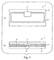
- Fig. 1 is an elevational view (A) and a sectional side elevation view (B) illustrating an example of a RFID tag.
- RFID tag 1 illustrated in Fig. 1 is constituted of an antenna 12 fitted onto a base 13 formed out of a sheet-like PET film or the like, an IC chip 11 connected to the antenna 12 through a bump 16 and a cover sheet 14 bonded to the base 13 using adhesives 15 with the antenna 12 and an IC chip 11 covered.
- An IC chip 11 constituting the RFID tag 1 can make radio communications with an external apparatus through the antenna 12 for information exchange.
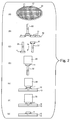
- Fig. 2 is a view illustrating a general IC chip mounting method, one of previously-proposed methods for RFID tags.
- one of a large amount of IC chips 11 on the wafer 10 is pulled and taken off from the tape 30 and held up using a picking jig 32.
- the IC chip 11 is transferred onto a bonding head 33.
- the bonding head 33 carries the IC chip 11 onto the base 13, places the chip on a proper position connected to the antenna 12 formed on the base 13 and, as illustrated in part (F) of Fig. 2, solders the IC chip 11 onto the base 13 by pressurizing and heating.
- the bonding head 33 is then moved from the IC chip 11, IC chip 11 mounting is completed as illustrated in part (G) of Fig. 2.
- Respective processes illustrated in parts (B) to (G) of Fig. 2 are sequentially repeated for a large amount of IC chips 11 on the wafer 10.
- this mounting method requires to sequentially perform, for each IC chip, a complicated process that the IC chips 11 on the wafer 10 are picked up one by one, inverted, delivered to another jig (bonding head) and mounted at the bonding head, thus impairing productivity and increasing manufacturing cost.
- Japanese Patent Laid-Open No. 2003-242472 has proposed that recessed portions for embedding IC chips are formed at intervals on a traveling web material (base), the IC chips are fitted into the recessed portions and antenna patterns are printed by means of an ink jet method so as to be connected with the IC chips fitted into the recessed portions.
- the method proposed by Japanese Patent Laid-Open No. 2003-242472 includes filling a tank with liquid to float the IC chips in the liquid and traveling the web material (base) through the tank inside to fit the IC chips into the recessed portions on the web material (base) in mounting the IC chips into the recessed portions on the web material (base) .
- the previously-proposed method has a problem of low process reliability of fitting the IC chips into the recessed portions because the IC chips are not always fitted exactly into the recessed portions in a proper direction and the recesses having no IC chips therein may pass through the tank inside. Even if the IC chips are properly fitted into the recessed portion, the antenna pattern needs to be positioned with high accuracy relative to the IC chips fitted into the recessed portions. Moreover, if a negligible error occurs at a position where the IC chips are fitted into the recessed portions, a printing position of the antenna pattern needs to be changed according to the error, which may not yield high productivity.
- An embodiment of a first aspect of IC chip mounting methods of the present invention is an IC chip mounting method for mounting two or more IC chips on a base, including the steps of:
- An embodiment of a second aspect of IC chip mounting methods of the present invention is an IC chip mounting method for mounting two or more IC chips on a base, including the steps of:
- An embodiment of a third aspect of IC chip mounting methods of the present invention is an IC chip mounting method for mounting two or more IC chips on a base, including the steps of:
- An embodiment of a fourth aspect of IC chip mounting methods of the present invention is an IC chip mounting method for mounting two or more IC chips on a base, including the steps of:
- the base is formed with two or more antennas for communication provided at prescribed intervals and each of the IC chips is mounted with a circuit for performing radio communication through each of the antennas positioned on the base.
- embodiments of the present invention may be applied to RFID tags.
- any one of the first to fourth IC chip mounting methods embodying the present invention it is preferable that mounting positions of the IC chips on the base and/or the IC chips themselves are shot with a camera and the IC chips are mounted on the base while position adjustment being made by image recognition.
- the first and the second IC chip mounting methods embodying the present invention respectively permit the IC chips to be sequentially mounted on the base at a high speed, thus enhancing productivity of IC chip mounting.
- the third and the fourth IC chip mounting methods embodying the present invention respectively permit two or more IC chips to be mounted on the base at a time or at a high speed sequentially because the IC chips are mounted on the base with intervals of the IC chips meeting intervals of mounting positions of the IC chips on the base, thus enhancing productivity of IC chip mounting.
- Fig. 3 is a view illustrating a relationship between a wafer and a base.
- the wafer 10 and the base 13 are prepared and are disposed at such positions that the wafer 10 and the base 13 face each other as illustrated in Fig. 3.
- the wafer 10 is divided into IC chips 11 by amounting a tape on a face (top face in Fig. 3) thereof which is the reverse of the wafer having a mounting surface (bottom face in Fig. 3) to be attached to the base 13, and leaving the tape 30 by dicing.
- the wafer 10, as illustrated in Fig. 3, is disposed at a position facing the base 13, in such a direction that the mounting surface to be attached to the base 13 faces the base 13.
- the wafer 10 is two-dimensionally moved in X and Y directions along the base 13.
- the base 13 is formed with two or more antennas 12 at prescribed intervals provided on a face (top face in Fig. 3) on the side facing the wafer 10 and is fed by a fixed amount in such a direction (indicated by arrow X in Fig. 3) that the antennas 12 align.
- the wafer 10 and the base 13 are disposed as illustrated in Fig. 3 and the IC chips 11 on the wafer 10 are mounted on the base 13 in the following way.
- Fig. 4 is a process diagram illustrating an IC chip mounting method according to the first embodiment of the present invention.
- the wafer 10 mounted with the tape 30 and divided into IC chips 11 is prepared for and is disposed facing the base 13 in such a direction that a mounting surface to the base 13 faces the base 13.
- the antennas 12 are arranged on the base 13 (part (A) of Fig. 4).
- Fig. 5 is a diagram showing a scene where IC chips 11 are positioned on the base 13.
- the IC chip 11 to be temporarily fixed is necessary to position at a prescribed position on the base 13.
- the IC chip 11 itself to be mounted and a mounting position of the IC chip 11 on the base 13 are shot with two cameras 71a, 71b and images thereof are recognized by respective image recognition sections 72a, 72b, respective deviation amounts are calculated by respective deviation amount calculation sections 73a, 73b.
- An XY correction section 74 exactly positions the IC chip to be mounted at a prescribed position on the base 13 by totalizing their deviation amounts. This permits the IC chip 11 to be exactly mounted at a prescribed position relative to the antenna 12 on the base 13.
- the wafer 10 is positioned by X-Y movement during feeding of the base 13 by a fixed amount (part (C) of Fig. 4), and the next IC chip 11b is pressed by the press-against jig 51 (part (D) of Fig. 4) and is temporarily fixed on the next antenna 12b positioned on the base 13 (part (E) of Fig. 4).
- the IC chip 11c is pressed against the antenna 12c positioned on the base 13 with the press-against jig 51 (part (F) of Fig. 4) in the same way and is temporarily fixed on the antenna 12c.
- a batch heating head 52 is placed on the IC chips 11, so that the IC chips 11 are heated and pressurized and solder-mounted on the respective antennas 12 positioned on the base 13 in a batch manner (part (G) of Fig. 4).
- the first embodiment permits two or more IC chips 11 to be temporarily fixed on the base 13 sequentially at a high speed and the IC chips 11 temporarily fixed on the base 13 to be solder-fixed in a batch manner by the batch heating head 52, thus accelerating mounting of the IC chips 11 on the base 13 for high productivity.
- Fig. 6 is a process diagram illustrating an IC chip mounting method according to the second embodiment of the present invention.
- the second embodiment uses the forms of arrangement and movement described referring to Fig. 3, which is left as it is.
- the wafer 10 mounted with the tape 30 and divided into IC chips 11 is prepared and is disposed so as to face the base 13 in such a direction that the mounting surface to be attached to the base 13 faces the base 13.
- the antennas 12 are arranged on the base 13 (part (A) of Fig. 6).
- Fig. 7 is a diagram showing a structure of the heating head 61.
- the heating head 61 includes a mounting head 611 at the central portion thereof.
- the mounting head 611 has a heater (not illustrated) therein and is so structured as to move vertically, retained by a head retainer 612.
- a sucking section 613 is provided so as to surround the mounting head 611. The sucking section 613 is sucked onto a periphery of the pressed-down IC chip 11 when the IC chip 11 is pressed down from the top of the tape 30 with the mounting head 611 as illustrated in part (B) of Fig. 7, so as to prevent an effect of the mounting head 611 pressing down the IC chip 11 to be pressed down from being exerted on a portion of the IC chip adjacent to the tape 30. This is because the effect exerted on the portion of the adjacent IC chip may cause an elongation of the tape to the portion of the adjacent IC chip to appear as a mounting position error at the time of mounting the IC chip.
- the wafer 10 side is positioned by X-Y movement during feeding of the base 13 by a fixed amount (part (C) of Fig. 6), and the next IC chip 11b is pressed by the heating head 61 (part (D) of Fig. 6) and is soldered onto the next antenna 12b positioned on the base 13 (part (E) of Fig. 6).
- the IC chip 11c is pressed against the antenna 12c positioned on the base 13 for heating and pressuring by the heating head 61 (part (F) of Fig. 6) in the same way and is soldered onto the antenna 12c.
- the second embodiment provides sequential and high-speed soldering of two or more IC chips 11 onto the two or more antennas 12 positioned on the base 13 respectively while the base 13 is delivered by a fixed amount and the wafer 10 is making X-Y movement, thus accelerating mounting of the IC chips 11 for high productivity.
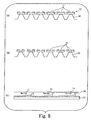
- Fig. 8 is a process diagram illustrating the third embodiment of the present invention.
- the tape 30 is in a contracted state by folding so that intervals between the IC chips 11 may meet intervals between mounting positions of the IC chips on the base 13 by development after dicing.
- Mounting the IC chips with the tape 30 contracting the wafer 10 is accomplished after positioning is performed so that each of top sections as ridges of folded sections of the tape 30 may meet each of the IC chips 11.
- the wafer 10 is diced so as to be divided into IC chips 11 (part (B) of Fig. 8).
- the IC chip 11 mounted with the tape 30 is made to face the base 13 in such a direction that the mounting surface (bottom face in part (C) of Fig. 8) of the IC chip 11 to the base 13 faces the base 13 under a developed state of the tape 30 (part (C) of Fig. 8).
- intervals between the IC chips 11 and intervals between the antennas 12 on the base 13 meet each other, thus eliminating need for individual positioning. Otherwise, even in the case of individual positioning as illustrated in Fig. 5, positioning may be slightly adjusted and the IC chips 11 may be fixed onto the respective antennas 12 on the base 13 in a batch manner or sequentially at a high speed.
- Fig. 9 is a process diagram illustrating the fourth embodiment of the present invention.
- the base 13 formed with the antennas 12 provided at equal intervals as illustrated in part (A) of Fig. 9 is contracted by folding as illustrated in part (B) of Fig. 9.
- the base 13 is mounted with IC chips 11 positioned on the wafer 10 on the base 13 by folding processing to develop the base 13, so that the base 13 is contracted in such a manner that intervals between the IC chips positioned on the base 13 may be equal to prescribed intervals between mounting positions of the IC chips 11 on the base 13, that is, intervals between the antennas 12.
- the wafer 10 is prepared such that a face of the wafer 10, which is the other side of the wafer 10 having a mounting surface to be attached to the base 13, is mounted with the tape 30; and the wafer is divided into IC chips 11 by dicing while leaving the tape 30.
- the wafer 10 is made to face the base 13 contracted in the above way in such a direction that the mounting surface to be attached to the base 13 faces the base 13 (part (C) of Fig. 9), and the IC chips 11 are mounted on the respective antennas 12 positioned on the base 13 (part (D) of Fig. 9).
- the IC chips 11 are mounted one by one on each of the antennas 12 formed on the base 13 at prescribed intervals (part (E) of Fig. 9).
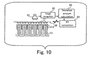
- Fig. 10 is a diagram showing a scene where the IC chips 11 are mounted on the base 13.
- a mounting portion of each of the IC chips is shot with a camera 81, an image thereof is recognized by an image recognition section 82, a deviation of the IC chip 11 from the antenna 12 on the base 13 is calculated by a deviation calculation section 83, and positioning of the IC chip 11 is adjusted by an XY correction section 84.
- the fourth embodiment provides mounting of the two or more IC chips 11 on the base 13 in a batch or sequentially at a high speed, thus accelerating IC chip mounting for mounting cost reduction.
Landscapes
- Engineering & Computer Science (AREA)
- Computer Hardware Design (AREA)
- Microelectronics & Electronic Packaging (AREA)
- Physics & Mathematics (AREA)
- General Physics & Mathematics (AREA)
- Theoretical Computer Science (AREA)
- Wire Bonding (AREA)
- Credit Cards Or The Like (AREA)
- Supply And Installment Of Electrical Components (AREA)
- Container, Conveyance, Adherence, Positioning, Of Wafer (AREA)
Abstract
Description
- The present invention relates to an IC chip mounting method for mounting two or more IC chips on a base.
- In recent years, various types of RFID tags have been proposed which exchange information with an external apparatus typified by a reader writer in a noncontact manner through electric waves. As one type of the RFID tags, there has been proposed a structure in which antenna patterns for radio communication and IC chips are mounted on a base sheet formed out of plastic or paper. For this type of RFID tags, there have been created usage patterns such as article identification by attaching the tag onto an article or the like and exchanging information about the article with the external apparatus.
- Fig. 1 is an elevational view (A) and a sectional side elevation view (B) illustrating an example of a RFID tag.
-
RFID tag 1 illustrated in Fig. 1 is constituted of anantenna 12 fitted onto abase 13 formed out of a sheet-like PET film or the like, anIC chip 11 connected to theantenna 12 through abump 16 and a cover sheet 14 bonded to thebase 13 usingadhesives 15 with theantenna 12 and anIC chip 11 covered. - An
IC chip 11 constituting theRFID tag 1 can make radio communications with an external apparatus through theantenna 12 for information exchange. - For the RFID tag, a wide range of usage patterns including the usage pattern described above have been created, however, use of the RFID tags in various types of usage patterns has a severe problem on manufacturing cost thereof, accordingly various efforts have been made for reduction in the manufacturing cost.
- Fig. 2 is a view illustrating a general IC chip mounting method, one of previously-proposed methods for RFID tags.
- As illustrated in part (A) of Fig. 2, the whole surface of a back side (the other face of a wafer having a mounting surface to be attached to a base sheet) of a
wafer 10 built out of various types of IC chips is mounted with atape 30 and further divided intoIC chips 11 leaving thetape 30 by dicing. - As illustrated in part (B) of Fig. 2, one of a large amount of
IC chips 11 on thewafer 10 is pulled and taken off from thetape 30 and held up using apicking jig 32. - As illustrated in part (C) of Fig. 2, the
picking jig 32 with theIC chip 11 sucked is turned upside down. - As illustrated in part (D) of Fig. 2, the
IC chip 11 is transferred onto abonding head 33. - Furthermore, as illustrated in part (E) of Fig. 2, the
bonding head 33 carries theIC chip 11 onto thebase 13, places the chip on a proper position connected to theantenna 12 formed on thebase 13 and, as illustrated in part (F) of Fig. 2, solders theIC chip 11 onto thebase 13 by pressurizing and heating. When thebonding head 33 is then moved from theIC chip 11,IC chip 11 mounting is completed as illustrated in part (G) of Fig. 2. - Respective processes illustrated in parts (B) to (G) of Fig. 2 are sequentially repeated for a large amount of
IC chips 11 on thewafer 10. - However, this mounting method requires to sequentially perform, for each IC chip, a complicated process that the
IC chips 11 on thewafer 10 are picked up one by one, inverted, delivered to another jig (bonding head) and mounted at the bonding head, thus impairing productivity and increasing manufacturing cost. - As one method for reducing the manufacturing cost,
Japanese Patent Laid-Open No. 2003-242472 - However, the method proposed by
Japanese Patent Laid-Open No. 2003-242472 - Accordingly, it is desirable to provide an IC chip mounting method capable of achieving high productivity.
- An embodiment of a first aspect of IC chip mounting methods of the present invention is an IC chip mounting method for mounting two or more IC chips on a base, including the steps of:
- preparing a wafer by mounting a tape on a face thereof, which is the reverse of the wafer having a mounting surface to be attached to the base, and by dividing the wafer into IC chips by dicing while leaving the tape;
- positioning the wafer to face the base in such a direction that the mounting surface to be attached to the base faces the base;
- sequentially pressing the IC chips on the wafer against the base and temporarily fixing the IC chips while the base is being fed in a prescribed one-dimensional direction along the wafer and while the wafer is being moved two-dimensionally along the base; and
- fixing the IC chips temporarily fixed on the base on the base by heating and pressurizing in a batch manner.
- An embodiment of a second aspect of IC chip mounting methods of the present invention is an IC chip mounting method for mounting two or more IC chips on a base, including the steps of:
- preparing a wafer by mounting a tape on a face thereof, which is the reverse of the wafer having a mounting surface to be attached to the base, and by dividing the wafer into IC chips by dicing while leaving the tape;
- positioning the wafer to face the base in such a direction that the mounting surface to be attached to the base faces the base; and
- sequentially fixing the IC chips on the base by pressing the IC chips on the wafer against the base for heating and pressurizing with a heating and pressurizing head which performs heating and pressurizing while the base is being fed in a prescribed one-dimensional direction along the wafer and while the wafer is being moved two-dimensionally along the base.
- An embodiment of a third aspect of IC chip mounting methods of the present invention is an IC chip mounting method for mounting two or more IC chips on a base, including the steps of:
- mounting a tape on a face of a wafer before the wafer is divided into IC chips by dicing, the face being the reverse of the wafer having a mounting surface to be attached to the base, and the tape being contracted by folding so that intervals between the IC chips may meet intervals between mounting positions of the IC chips onto the base by development after the dicing,
- dividing the wafer mounted with the contracted tape into IC chips by dicing while leaving the tape; and
- positioning the IC chip mounted with the tape to face the base under a developed state of the tape in such a direction that the mounting surface of the IC chip to the base faces the base; and
- mounting the IC chip on the base.
- An embodiment of a fourth aspect of IC chip mounting methods of the present invention is an IC chip mounting method for mounting two or more IC chips on a base, including the steps of:
- preparing a wafer by mounting a tape on a face, which is the reverse of the wafer having a mounting surface to be attached to the base, and by dividing the wafer into IC chips by dicing while leaving the tape, and contracting the base to be mounted with the IC chips by folding so that intervals between mounting positions of the IC chips on the base may be the same as prescribed intervals between mounting positions of the IC chips on the base by mounting the IC chips positioned on the wafer on the base and developing the base;
- positioning the wafer mounted with the tape to face the contracted base in such a direction that the mounting surface to be attached to the base faces the base;
- mounting the IC chips on the wafer on the contarcted base; and
- developing the base.
- In any one of the first to fourth IC chip mounting methods embodying the present invention, it is preferable that the base is formed with two or more antennas for communication provided at prescribed intervals and each of the IC chips is mounted with a circuit for performing radio communication through each of the antennas positioned on the base. In other words, embodiments of the present invention may be applied to RFID tags.
- In any one of the first to fourth IC chip mounting methods embodying the present invention, it is preferable that mounting positions of the IC chips on the base and/or the IC chips themselves are shot with a camera and the IC chips are mounted on the base while position adjustment being made by image recognition.
- The first and the second IC chip mounting methods embodying the present invention respectively permit the IC chips to be sequentially mounted on the base at a high speed, thus enhancing productivity of IC chip mounting.
- Moreover, the third and the fourth IC chip mounting methods embodying the present invention respectively permit two or more IC chips to be mounted on the base at a time or at a high speed sequentially because the IC chips are mounted on the base with intervals of the IC chips meeting intervals of mounting positions of the IC chips on the base, thus enhancing productivity of IC chip mounting.
-
- Fig. 1 is an elevational view (A) and a sectional side elevation view (B) illustrating an example of a RFID tag;
- Fig. 2 is a view illustrating a general IC chip mounting method, one of previously-proposed methods for RFID tags.
- Fig. 3 is a view illustrating a relationship between a wafer and a base;
- Fig. 4 is a process diagram illustrating an IC chip mounting method according to the first embodiment of the present invention;
- Fig. 5 is a diagram showing a scene where IC chips are mounted on a base;
- Fig. 6 is a process diagram illustrating an IC chip mounting method according to the second embodiment of the present invention;
- Fig. 7 is a diagram showing a structure of a heating head;
- Fig. 8 is a process diagram illustrating the third embodiment of the present invention;
- Fig. 9 is a process diagram illustrating the fourth embodiment of the present invention; and
- Fig. 10 is a diagram showing a scene where IC chips are mounted on a base.
- Embodiments of the present invention will be described below.
- Fig. 3 is a view illustrating a relationship between a wafer and a base.
- In the first embodiment described below, the
wafer 10 and thebase 13 are prepared and are disposed at such positions that thewafer 10 and thebase 13 face each other as illustrated in Fig. 3. Thewafer 10 is divided intoIC chips 11 by amounting a tape on a face (top face in Fig. 3) thereof which is the reverse of the wafer having a mounting surface (bottom face in Fig. 3) to be attached to thebase 13, and leaving thetape 30 by dicing. Thewafer 10, as illustrated in Fig. 3, is disposed at a position facing thebase 13, in such a direction that the mounting surface to be attached to the base 13 faces thebase 13. Thewafer 10 is two-dimensionally moved in X and Y directions along thebase 13. - The
base 13 is formed with two ormore antennas 12 at prescribed intervals provided on a face (top face in Fig. 3) on the side facing thewafer 10 and is fed by a fixed amount in such a direction (indicated by arrow X in Fig. 3) that theantennas 12 align. - In the first embodiment of the present invention, the
wafer 10 and the base 13 are disposed as illustrated in Fig. 3 and the IC chips 11 on thewafer 10 are mounted on the base 13 in the following way. - Fig. 4 is a process diagram illustrating an IC chip mounting method according to the first embodiment of the present invention.
- As described in reference to Fig. 3, first, the
wafer 10 mounted with thetape 30 and divided intoIC chips 11 is prepared for and is disposed facing the base 13 in such a direction that a mounting surface to the base 13 faces thebase 13. On the other hand, theantennas 12 are arranged on the base 13 (part (A) of Fig. 4). - By two-dimensionally moving the
wafer 10 in X and Y directions (refer to Fig. 3) under such a condition that while thebase 13 is being fed by a fixed amount in a direction of an arrow X (refer to Fig. 3), one (IC chip 11a) of a large amount ofIC chips 11 aligning on thewafer 10 is pressed from the top of thetape 30 with a press-againstjig 51 and theIC chip 11a is temporarily fixed on oneantenna 12a positioned on the base 13 (part (B) of Fig. 4). - Fig. 5 is a diagram showing a scene where IC chips 11 are positioned on the
base 13. - In temporarily fixing the IC chips 11 on the
base 13 by pressing each of the IC chips 11 with the press-againstjig 51, theIC chip 11 to be temporarily fixed is necessary to position at a prescribed position on thebase 13. TheIC chip 11 itself to be mounted and a mounting position of theIC chip 11 on thebase 13 are shot with twocameras image recognition sections amount calculation sections XY correction section 74 exactly positions the IC chip to be mounted at a prescribed position on thebase 13 by totalizing their deviation amounts. This permits theIC chip 11 to be exactly mounted at a prescribed position relative to theantenna 12 on thebase 13. - The description of this embodiment will be made, returning to Fig. 4.
- Next, the
wafer 10 is positioned by X-Y movement during feeding of the base 13 by a fixed amount (part (C) of Fig. 4), and thenext IC chip 11b is pressed by the press-against jig 51 (part (D) of Fig. 4) and is temporarily fixed on thenext antenna 12b positioned on the base 13 (part (E) of Fig. 4). - Next, the
IC chip 11c is pressed against theantenna 12c positioned on the base 13 with the press-against jig 51 (part (F) of Fig. 4) in the same way and is temporarily fixed on theantenna 12c. - After the IC chips 11 are temporarily fixed on the
antennas 12 positioned on the base 13 respectively in this way, abatch heating head 52 is placed on the IC chips 11, so that the IC chips 11 are heated and pressurized and solder-mounted on therespective antennas 12 positioned on the base 13 in a batch manner (part (G) of Fig. 4). - The first embodiment permits two or
more IC chips 11 to be temporarily fixed on the base 13 sequentially at a high speed and the IC chips 11 temporarily fixed on the base 13 to be solder-fixed in a batch manner by thebatch heating head 52, thus accelerating mounting of the IC chips 11 on thebase 13 for high productivity. - Fig. 6 is a process diagram illustrating an IC chip mounting method according to the second embodiment of the present invention.
- The second embodiment uses the forms of arrangement and movement described referring to Fig. 3, which is left as it is. In other words, as illustrated in Fig. 3, first, the
wafer 10 mounted with thetape 30 and divided intoIC chips 11 is prepared and is disposed so as to face the base 13 in such a direction that the mounting surface to be attached to the base 13 faces thebase 13. On the other hand, theantennas 12 are arranged on the base 13 (part (A) of Fig. 6). - By two-dimensionally moving the
wafer 10 in X and Y directions (refer to Fig. 3) under such a condition that while thebase 13 is being fed by a fixed amount in a direction of an arrow X (refer to Fig. 3), one (IC chip 11a) of a large amount ofIC chips 11 aligning on thewafer 10 is pressed from the top of thetape 30 with aheating head 61 for heating and pressurizing, and theIC chip 11a is soldered onto oneantenna 12a positioned on the base 13 (part (B) of Fig. 6). - Fig. 7 is a diagram showing a structure of the
heating head 61. - The
heating head 61 includes a mountinghead 611 at the central portion thereof. The mountinghead 611 has a heater (not illustrated) therein and is so structured as to move vertically, retained by ahead retainer 612. A suckingsection 613 is provided so as to surround the mountinghead 611. The suckingsection 613 is sucked onto a periphery of the pressed-downIC chip 11 when theIC chip 11 is pressed down from the top of thetape 30 with the mountinghead 611 as illustrated in part (B) of Fig. 7, so as to prevent an effect of the mountinghead 611 pressing down theIC chip 11 to be pressed down from being exerted on a portion of the IC chip adjacent to thetape 30. This is because the effect exerted on the portion of the adjacent IC chip may cause an elongation of the tape to the portion of the adjacent IC chip to appear as a mounting position error at the time of mounting the IC chip. - A description of this embodiment will be made, returning to Fig. 6.
- Next, the
wafer 10 side is positioned by X-Y movement during feeding of the base 13 by a fixed amount (part (C) of Fig. 6), and thenext IC chip 11b is pressed by the heating head 61 (part (D) of Fig. 6) and is soldered onto thenext antenna 12b positioned on the base 13 (part (E) of Fig. 6). - Next, the
IC chip 11c is pressed against theantenna 12c positioned on thebase 13 for heating and pressuring by the heating head 61 (part (F) of Fig. 6) in the same way and is soldered onto theantenna 12c. - In this way, the second embodiment provides sequential and high-speed soldering of two or
more IC chips 11 onto the two ormore antennas 12 positioned on the base 13 respectively while thebase 13 is delivered by a fixed amount and thewafer 10 is making X-Y movement, thus accelerating mounting of the IC chips 11 for high productivity. - Fig. 8 is a process diagram illustrating the third embodiment of the present invention.
- A face (top face in part (A) of Fig. 8) of the
wafer 10 before being divided into two ormore IC chips 11, which is the reverse of thewafer 10 having the mounting surface (bottom face in part (A) of Fig. 8) to be attached to the base 13 (refer to part (C) of Fig. 8), is mounted with the tape 30 (part (A) of Fig. 8). Thetape 30 is in a contracted state by folding so that intervals between the IC chips 11 may meet intervals between mounting positions of the IC chips on thebase 13 by development after dicing. - Mounting the IC chips with the
tape 30 contracting thewafer 10 is accomplished after positioning is performed so that each of top sections as ridges of folded sections of thetape 30 may meet each of the IC chips 11. - Subsequently, the
wafer 10 is diced so as to be divided into IC chips 11 (part (B) of Fig. 8). - The
IC chip 11 mounted with thetape 30 is made to face the base 13 in such a direction that the mounting surface (bottom face in part (C) of Fig. 8) of theIC chip 11 to the base 13 faces thebase 13 under a developed state of the tape 30 (part (C) of Fig. 8). - Under this state, intervals between the IC chips 11 and intervals between the
antennas 12 on the base 13 meet each other, thus eliminating need for individual positioning. Otherwise, even in the case of individual positioning as illustrated in Fig. 5, positioning may be slightly adjusted and the IC chips 11 may be fixed onto therespective antennas 12 on the base 13 in a batch manner or sequentially at a high speed. - Fig. 9 is a process diagram illustrating the fourth embodiment of the present invention.
- The base 13 formed with the
antennas 12 provided at equal intervals as illustrated in part (A) of Fig. 9 is contracted by folding as illustrated in part (B) of Fig. 9. Thebase 13 is mounted withIC chips 11 positioned on thewafer 10 on thebase 13 by folding processing to develop thebase 13, so that thebase 13 is contracted in such a manner that intervals between the IC chips positioned on thebase 13 may be equal to prescribed intervals between mounting positions of the IC chips 11 on thebase 13, that is, intervals between theantennas 12. - In addition to the base, the
wafer 10 is prepared such that a face of thewafer 10, which is the other side of thewafer 10 having a mounting surface to be attached to thebase 13, is mounted with thetape 30; and the wafer is divided intoIC chips 11 by dicing while leaving thetape 30. Thewafer 10 is made to face the base 13 contracted in the above way in such a direction that the mounting surface to be attached to the base 13 faces the base 13 (part (C) of Fig. 9), and the IC chips 11 are mounted on therespective antennas 12 positioned on the base 13 (part (D) of Fig. 9). Then, when thebase 13 is developed, the IC chips 11 are mounted one by one on each of theantennas 12 formed on the base 13 at prescribed intervals (part (E) of Fig. 9). - Fig. 10 is a diagram showing a scene where the IC chips 11 are mounted on the
base 13. - In mounting the IC chips 11 on the
base 13, a mounting portion of each of the IC chips is shot with acamera 81, an image thereof is recognized by animage recognition section 82, a deviation of theIC chip 11 from theantenna 12 on thebase 13 is calculated by adeviation calculation section 83, and positioning of theIC chip 11 is adjusted by anXY correction section 84. This permits theIC chip 11 to be exactly mounted at a prescribed position relative to theantenna 12 on thebase 13. - The fourth embodiment provides mounting of the two or more IC chips 11 on the base 13 in a batch or sequentially at a high speed, thus accelerating IC chip mounting for mounting cost reduction.
Claims (6)
- An IC chip mounting method which mounts two or more IC chips on a base, comprising the steps of:preparing a wafer by mounting a tape on a face thereof, which is the reverse of the wafer having a mounting surface to be attached to the base, and by dividing the wafer into IC chips by dicing while leaving the tape;positioning the wafer to face the base in such a direction that the mounting surface to be attached to the base faces the base;sequentially pressing the IC chips on the wafer against the base and temporarily fixing the IC chips while the base is being fed in a prescribed one-dimensional direction along the wafer and while the wafer is being moved two-dimensionally along the base; andfixing the IC chips temporarily fixed on the base on the base by heating and pressurizing in a batch manner.
- An IC chip mounting method which mounts two or more IC chips on a base, comprising the steps of:preparing a wafer by mounting a tape on a face thereof, which is the reverse of the wafer having a mounting surface to be attached to the base, and by dividing the wafer into IC chips by dicing while leaving the tape;positioning the wafer to face the base in such a direction that the mounting surface to be attached to the base faces the base; andsequentially fixing the IC chips on the base by pressing the IC chips on the wafer against the base for heating and pressurizing with a heating and pressurizing head which performs heating and pressurizing while the base is being fed in a prescribed one-dimensional direction along the wafer and while the wafer is being moved two-dimensionally along the base.
- An IC chip mounting method which mounts two or more IC chips on a base, comprising the steps of:mounting a tape on a face of a wafer before the wafer is divided into IC chips by dicing, the face being the reverse of the wafer having a mounting surface to be attached to the base, and the tape being contracted by folding so that intervals between the IC chips may meet intervals between mounting positions of the IC chips onto the base by development after the dicing,dividing the wafer mounted with the contracted tape into IC chips by dicing while leaving the tape; andpositioning the IC chip mounted with the tape to face the base under a developed state of the tape in such a direction that the mounting surface of the IC chip to the base faces the base; andmounting the IC chip on the base.
- An IC chip mounting method which mounts two or more IC chips on a base, comprising the steps of:preparing a wafer by mounting a tape on a face, which is the reverse of the wafer having a mounting surface to be attached to the base, and by dividing the wafer into IC chips by dicing while leaving the tape, and contracting the base to be mounted with the IC chips by folding so that intervals between mounting positions of the IC chips on the base may be the same as prescribed intervals between mounting positions of the IC chips on the base by mounting the IC chips positioned on the wafer on the base and developing the base;positioning the wafer mounted with the tape to face the contracted base in such a direction that the mounting surface to be attached to the base faces the base;mounting the IC chips on the wafer on the contarcted base; anddeveloping the base.
- An IC chip mounting method according to any preceding claim, wherein the base is formed with two or more antennas for communication provided at prescribed intervals, and
each of the IC chips is mounted with a circuit which performs radio communication through each of the antennas positioned on the base. - An IC chip mounting method according to any preceding claim, wherein mounting positions of the IC chips on the base and/or the IC chips themselves are shot with a camera and the IC chips are mounted on the base while position adjustment being made by image recognition, in mounting the IC chips facing the base on the base.
Applications Claiming Priority (1)
| Application Number | Priority Date | Filing Date | Title |
|---|---|---|---|
| JP2005209965A JP4750492B2 (en) | 2005-07-20 | 2005-07-20 | IC chip mounting method |
Publications (3)
| Publication Number | Publication Date |
|---|---|
| EP1746651A2 true EP1746651A2 (en) | 2007-01-24 |
| EP1746651A3 EP1746651A3 (en) | 2007-04-18 |
| EP1746651B1 EP1746651B1 (en) | 2016-09-28 |
Family
ID=37330695
Family Applications (1)
| Application Number | Title | Priority Date | Filing Date |
|---|---|---|---|
| EP05257725.1A Expired - Lifetime EP1746651B1 (en) | 2005-07-20 | 2005-12-15 | IC chip mounting method |
Country Status (6)
| Country | Link |
|---|---|
| US (1) | US7214563B2 (en) |
| EP (1) | EP1746651B1 (en) |
| JP (1) | JP4750492B2 (en) |
| KR (2) | KR100824083B1 (en) |
| CN (2) | CN100431125C (en) |
| TW (1) | TWI315052B (en) |
Cited By (1)
| Publication number | Priority date | Publication date | Assignee | Title |
|---|---|---|---|---|
| FR3118514A1 (en) * | 2020-12-31 | 2022-07-01 | Axem Technology | Method of manufacturing an RFID identifier |
Families Citing this family (23)
| Publication number | Priority date | Publication date | Assignee | Title |
|---|---|---|---|---|
| JP2011222639A (en) * | 2010-04-07 | 2011-11-04 | Disco Abrasive Syst Ltd | Bonding method |
| JP2012156473A (en) * | 2011-01-28 | 2012-08-16 | Adwelds:Kk | Component transfer device and component transfer method |
| KR101801264B1 (en) | 2011-06-13 | 2017-11-27 | 삼성전자주식회사 | Apparatus of manufacturing semiconductor and Method for packaging semiconductor using the same |
| KR101288165B1 (en) * | 2011-08-29 | 2013-07-18 | 삼성전기주식회사 | Stamping device for biochip and stamping method |
| JP2014033100A (en) * | 2012-08-03 | 2014-02-20 | Panasonic Corp | Implementation method |
| KR101488609B1 (en) * | 2013-07-22 | 2015-01-30 | 앰코 테크놀로지 코리아 주식회사 | Manufacturing method of semiconductor device |
| JP6367084B2 (en) * | 2014-10-30 | 2018-08-01 | 株式会社東芝 | Semiconductor chip bonding method and semiconductor chip bonding apparatus |
| JP6582975B2 (en) * | 2015-12-28 | 2019-10-02 | 富士通株式会社 | Semiconductor mounting apparatus, head of semiconductor mounting apparatus, and manufacturing method of laminated chip |
| US10672638B2 (en) * | 2017-01-27 | 2020-06-02 | International Business Machines Corporation | Picking up irregular semiconductor chips |
| US10694651B2 (en) * | 2017-06-20 | 2020-06-23 | Saul Tech Technology Co., Ltd. | Chip-placing method performing an image alignment for chip placement and chip-placing apparatus thereof |
| KR102077049B1 (en) * | 2017-12-21 | 2020-02-13 | 한국기계연구원 | Method of transferring micro device and apparatus for transferring micro device |
| WO2019177337A1 (en) | 2018-03-12 | 2019-09-19 | (주)큐엠씨 | Transfer apparatus and method for transferring light-emitting diode chip |
| KR102139571B1 (en) * | 2018-03-12 | 2020-07-29 | ㈜큐엠씨 | Method and apparatus for transfferring light emitting diode chip |
| KR102031603B1 (en) * | 2018-03-12 | 2019-11-08 | ㈜큐엠씨 | Method and apparatus for transfferring light emitting diode chip |
| JP6906586B2 (en) * | 2018-06-21 | 2021-07-21 | 株式会社東芝 | Semiconductor chip joining method and semiconductor chip joining device |
| US11069555B2 (en) * | 2018-09-03 | 2021-07-20 | Assembleon B.V. | Die attach systems, and methods of attaching a die to a substrate |
| KR20200109493A (en) * | 2019-03-13 | 2020-09-23 | (주)큐엠씨 | Apparatus and method for transferring semiconductor chip |
| CN109830453B (en) * | 2019-03-21 | 2023-10-03 | 深圳中科四合科技有限公司 | Method and device for transferring huge amount of chips |
| US11136202B2 (en) * | 2020-01-06 | 2021-10-05 | Asm Technology Singapore Pte Ltd | Direct transfer apparatus for electronic components |
| KR102391169B1 (en) * | 2020-03-11 | 2022-05-03 | 넥스타테크놀로지 주식회사 | Mounting head and apparatus for mounting component comprising the same |
| KR102436955B1 (en) * | 2020-03-11 | 2022-08-26 | 넥스타테크놀로지 주식회사 | Mounting head and apparatus for mounting component comprising the same |
| KR102271499B1 (en) * | 2020-10-16 | 2021-07-01 | 넥스타테크놀로지 주식회사 | Mounting head and apparatus for mounting component comprising the same |
| KR102880205B1 (en) * | 2021-06-21 | 2025-11-04 | 에스케이하이닉스 주식회사 | Semiconductor processing apparatus and method of manufacturing semiconductor device using the same |
Citations (1)
| Publication number | Priority date | Publication date | Assignee | Title |
|---|---|---|---|---|
| JP2003242472A (en) | 2002-02-14 | 2003-08-29 | Dainippon Printing Co Ltd | Method for forming antenna pattern and printed circuit on IC chip mounted on web, and package with IC tag |
Family Cites Families (15)
| Publication number | Priority date | Publication date | Assignee | Title |
|---|---|---|---|---|
| JPH0232548A (en) * | 1988-07-22 | 1990-02-02 | Hitachi Ltd | Pellet bonding of film package type semiconductor device |
| JPH06204267A (en) * | 1993-01-08 | 1994-07-22 | Nec Yamagata Ltd | Manufacture of semiconductor device |
| JP3955659B2 (en) * | 1997-06-12 | 2007-08-08 | リンテック株式会社 | Electronic component die bonding method and die bonding apparatus used therefor |
| JP3994498B2 (en) * | 1998-01-30 | 2007-10-17 | 日立化成工業株式会社 | Manufacturing method of semiconductor device |
| US6313522B1 (en) * | 1998-08-28 | 2001-11-06 | Micron Technology, Inc. | Semiconductor structure having stacked semiconductor devices |
| JP4137351B2 (en) * | 2000-06-29 | 2008-08-20 | 芝浦メカトロニクス株式会社 | Component mounting equipment |
| JP2002026071A (en) * | 2000-07-05 | 2002-01-25 | Seiko Epson Corp | Semiconductor device and its manufacturing method, circuit board, and electronic equipment |
| CN1149650C (en) * | 2001-04-16 | 2004-05-12 | 华瑞股份有限公司 | Flip chip mounting method of power field effect transistor for rechargeable battery protection circuit |
| DE10121578C2 (en) * | 2001-05-03 | 2003-04-10 | Infineon Technologies Ag | Method and assembly system for assembling a substrate with electronic components |
| JP4000791B2 (en) * | 2001-06-15 | 2007-10-31 | 株式会社日立製作所 | Manufacturing method of semiconductor device |
| US6940729B2 (en) * | 2001-10-26 | 2005-09-06 | Staktek Group L.P. | Integrated circuit stacking system and method |
| US6965160B2 (en) * | 2002-08-15 | 2005-11-15 | Micron Technology, Inc. | Semiconductor dice packages employing at least one redistribution layer |
| US7246431B2 (en) * | 2002-09-06 | 2007-07-24 | Tessera, Inc. | Methods of making microelectronic packages including folded substrates |
| US7575955B2 (en) * | 2004-01-06 | 2009-08-18 | Ismat Corporation | Method for making electronic packages |
| JP2006196526A (en) * | 2005-01-11 | 2006-07-27 | Omron Corp | Semiconductor chip mounting method, printed circuit board structure, and printed circuit board manufacturing method |
-
2005
- 2005-07-20 JP JP2005209965A patent/JP4750492B2/en not_active Expired - Fee Related
- 2005-12-14 TW TW094144237A patent/TWI315052B/en not_active IP Right Cessation
- 2005-12-15 EP EP05257725.1A patent/EP1746651B1/en not_active Expired - Lifetime
- 2005-12-29 US US11/319,652 patent/US7214563B2/en not_active Expired - Fee Related
-
2006
- 2006-01-04 KR KR1020060001010A patent/KR100824083B1/en not_active Expired - Fee Related
- 2006-01-09 CN CNB2006100036140A patent/CN100431125C/en not_active Expired - Fee Related
- 2006-01-09 CN CN2008100992976A patent/CN101303988B/en not_active Expired - Fee Related
-
2007
- 2007-11-13 KR KR1020070115728A patent/KR100811039B1/en not_active Expired - Fee Related
Patent Citations (1)
| Publication number | Priority date | Publication date | Assignee | Title |
|---|---|---|---|---|
| JP2003242472A (en) | 2002-02-14 | 2003-08-29 | Dainippon Printing Co Ltd | Method for forming antenna pattern and printed circuit on IC chip mounted on web, and package with IC tag |
Cited By (2)
| Publication number | Priority date | Publication date | Assignee | Title |
|---|---|---|---|---|
| FR3118514A1 (en) * | 2020-12-31 | 2022-07-01 | Axem Technology | Method of manufacturing an RFID identifier |
| WO2022144517A1 (en) * | 2020-12-31 | 2022-07-07 | Axem Technology | Process for manufacturing an rfid |
Also Published As
| Publication number | Publication date |
|---|---|
| CN100431125C (en) | 2008-11-05 |
| CN101303988A (en) | 2008-11-12 |
| EP1746651A3 (en) | 2007-04-18 |
| KR20070011066A (en) | 2007-01-24 |
| TW200705280A (en) | 2007-02-01 |
| KR100824083B1 (en) | 2008-04-21 |
| KR20070115835A (en) | 2007-12-06 |
| TWI315052B (en) | 2009-09-21 |
| EP1746651B1 (en) | 2016-09-28 |
| US7214563B2 (en) | 2007-05-08 |
| JP2007027549A (en) | 2007-02-01 |
| KR100811039B1 (en) | 2008-03-07 |
| JP4750492B2 (en) | 2011-08-17 |
| CN101303988B (en) | 2012-02-08 |
| CN1901147A (en) | 2007-01-24 |
| US20070020800A1 (en) | 2007-01-25 |
Similar Documents
| Publication | Publication Date | Title |
|---|---|---|
| EP1746651B1 (en) | IC chip mounting method | |
| US7595219B2 (en) | IC chip mounting method for mounting two or more IC chips by sequentially transferring the IC chips sucked onto a first roller to a second roller and mounting the IC chips transferred to the second roller on a traveling base | |
| CN101251903B (en) | radio frequency identification tag | |
| US11937375B2 (en) | Wireless communication device manufacturing method and wireless communication device manufacturing apparatus | |
| CN100538731C (en) | RFID tag manufacturing method and RFID tag | |
| KR100979736B1 (en) | Electronic device manufacturing system and electronic device manufacturing method | |
| JP2005209144A (en) | IC chip mounting body manufacturing method and manufacturing apparatus | |
| JP2017183378A (en) | Electronic component mounting equipment | |
| EP1703448A2 (en) | RFID tag, module component, and RFID tag fabrication method | |
| JP2003069294A (en) | IC chip mounting device | |
| KR100636657B1 (en) | Dual press punching device for punching each sheet constituting the IC card sheet | |
| JP2004014914A (en) | Substrate pasting device, substrate pasting method and card manufacturing device |
Legal Events
| Date | Code | Title | Description |
|---|---|---|---|
| PUAI | Public reference made under article 153(3) epc to a published international application that has entered the european phase |
Free format text: ORIGINAL CODE: 0009012 |
|
| AK | Designated contracting states |
Kind code of ref document: A2 Designated state(s): AT BE BG CH CY CZ DE DK EE ES FI FR GB GR HU IE IS IT LI LT LU LV MC NL PL PT RO SE SI SK TR |
|
| AX | Request for extension of the european patent |
Extension state: AL BA HR MK YU |
|
| PUAL | Search report despatched |
Free format text: ORIGINAL CODE: 0009013 |
|
| RTI1 | Title (correction) |
Free format text: IC CHIP MOUNTING METHOD |
|
| AK | Designated contracting states |
Kind code of ref document: A3 Designated state(s): AT BE BG CH CY CZ DE DK EE ES FI FR GB GR HU IE IS IT LI LT LU LV MC NL PL PT RO SE SI SK TR |
|
| AX | Request for extension of the european patent |
Extension state: AL BA HR MK YU |
|
| 17P | Request for examination filed |
Effective date: 20071015 |
|
| AKX | Designation fees paid |
Designated state(s): DE FR GB |
|
| 17Q | First examination report despatched |
Effective date: 20140618 |
|
| REG | Reference to a national code |
Ref country code: DE Ref legal event code: R079 Ref document number: 602005050300 Country of ref document: DE Free format text: PREVIOUS MAIN CLASS: H01L0023498000 Ipc: H01L0021000000 |
|
| GRAP | Despatch of communication of intention to grant a patent |
Free format text: ORIGINAL CODE: EPIDOSNIGR1 |
|
| RIC1 | Information provided on ipc code assigned before grant |
Ipc: G06K 19/077 20060101ALI20160404BHEP Ipc: H01L 21/00 20060101AFI20160404BHEP Ipc: H01L 23/00 20060101ALI20160404BHEP Ipc: H01L 21/683 20060101ALI20160404BHEP Ipc: H01L 21/67 20060101ALI20160404BHEP Ipc: H01L 23/498 20060101ALI20160404BHEP |
|
| INTG | Intention to grant announced |
Effective date: 20160426 |
|
| GRAS | Grant fee paid |
Free format text: ORIGINAL CODE: EPIDOSNIGR3 |
|
| GRAA | (expected) grant |
Free format text: ORIGINAL CODE: 0009210 |
|
| AK | Designated contracting states |
Kind code of ref document: B1 Designated state(s): DE FR GB |
|
| REG | Reference to a national code |
Ref country code: GB Ref legal event code: FG4D |
|
| REG | Reference to a national code |
Ref country code: DE Ref legal event code: R096 Ref document number: 602005050300 Country of ref document: DE |
|
| REG | Reference to a national code |
Ref country code: FR Ref legal event code: PLFP Year of fee payment: 12 |
|
| PGFP | Annual fee paid to national office [announced via postgrant information from national office to epo] |
Ref country code: DE Payment date: 20160929 Year of fee payment: 12 Ref country code: GB Payment date: 20161005 Year of fee payment: 12 |
|
| REG | Reference to a national code |
Ref country code: DE Ref legal event code: R097 Ref document number: 602005050300 Country of ref document: DE |
|
| PLBE | No opposition filed within time limit |
Free format text: ORIGINAL CODE: 0009261 |
|
| STAA | Information on the status of an ep patent application or granted ep patent |
Free format text: STATUS: NO OPPOSITION FILED WITHIN TIME LIMIT |
|
| 26N | No opposition filed |
Effective date: 20170629 |
|
| REG | Reference to a national code |
Ref country code: FR Ref legal event code: PLFP Year of fee payment: 13 |
|
| PGFP | Annual fee paid to national office [announced via postgrant information from national office to epo] |
Ref country code: FR Payment date: 20171113 Year of fee payment: 13 |
|
| REG | Reference to a national code |
Ref country code: DE Ref legal event code: R119 Ref document number: 602005050300 Country of ref document: DE |
|
| GBPC | Gb: european patent ceased through non-payment of renewal fee |
Effective date: 20171215 |
|
| PG25 | Lapsed in a contracting state [announced via postgrant information from national office to epo] |
Ref country code: DE Free format text: LAPSE BECAUSE OF NON-PAYMENT OF DUE FEES Effective date: 20180703 |
|
| PG25 | Lapsed in a contracting state [announced via postgrant information from national office to epo] |
Ref country code: GB Free format text: LAPSE BECAUSE OF NON-PAYMENT OF DUE FEES Effective date: 20171215 |
|
| PG25 | Lapsed in a contracting state [announced via postgrant information from national office to epo] |
Ref country code: FR Free format text: LAPSE BECAUSE OF NON-PAYMENT OF DUE FEES Effective date: 20181231 |