EP1746641A1 - Gruppe iii-nitrid-halbleiterbauelement und epitaktisches substrat - Google Patents
Gruppe iii-nitrid-halbleiterbauelement und epitaktisches substrat Download PDFInfo
- Publication number
- EP1746641A1 EP1746641A1 EP06715178A EP06715178A EP1746641A1 EP 1746641 A1 EP1746641 A1 EP 1746641A1 EP 06715178 A EP06715178 A EP 06715178A EP 06715178 A EP06715178 A EP 06715178A EP 1746641 A1 EP1746641 A1 EP 1746641A1
- Authority
- EP
- European Patent Office
- Prior art keywords
- epitaxial
- substrate
- epitaxial layer
- layer
- algan
- Prior art date
- Legal status (The legal status is an assumption and is not a legal conclusion. Google has not performed a legal analysis and makes no representation as to the accuracy of the status listed.)
- Granted
Links
Images


Classifications
-
- H—ELECTRICITY
- H10—SEMICONDUCTOR DEVICES; ELECTRIC SOLID-STATE DEVICES NOT OTHERWISE PROVIDED FOR
- H10D—INORGANIC ELECTRIC SEMICONDUCTOR DEVICES
- H10D30/00—Field-effect transistors [FET]
- H10D30/01—Manufacture or treatment
- H10D30/015—Manufacture or treatment of FETs having heterojunction interface channels or heterojunction gate electrodes, e.g. HEMT
-
- H—ELECTRICITY
- H10—SEMICONDUCTOR DEVICES; ELECTRIC SOLID-STATE DEVICES NOT OTHERWISE PROVIDED FOR
- H10P—GENERIC PROCESSES OR APPARATUS FOR THE MANUFACTURE OR TREATMENT OF DEVICES COVERED BY CLASS H10
- H10P10/00—Bonding of wafers, substrates or parts of devices
-
- H—ELECTRICITY
- H10—SEMICONDUCTOR DEVICES; ELECTRIC SOLID-STATE DEVICES NOT OTHERWISE PROVIDED FOR
- H10D—INORGANIC ELECTRIC SEMICONDUCTOR DEVICES
- H10D30/00—Field-effect transistors [FET]
- H10D30/40—FETs having zero-dimensional [0D], one-dimensional [1D] or two-dimensional [2D] charge carrier gas channels
- H10D30/47—FETs having zero-dimensional [0D], one-dimensional [1D] or two-dimensional [2D] charge carrier gas channels having two-dimensional [2D] charge carrier gas channels, e.g. nanoribbon FETs or high electron mobility transistors [HEMT]
- H10D30/471—High electron mobility transistors [HEMT] or high hole mobility transistors [HHMT]
- H10D30/475—High electron mobility transistors [HEMT] or high hole mobility transistors [HHMT] having wider bandgap layer formed on top of lower bandgap active layer, e.g. undoped barrier HEMTs such as i-AlGaN/GaN HEMTs
- H10D30/4755—High electron mobility transistors [HEMT] or high hole mobility transistors [HHMT] having wider bandgap layer formed on top of lower bandgap active layer, e.g. undoped barrier HEMTs such as i-AlGaN/GaN HEMTs having wide bandgap charge-carrier supplying layers, e.g. modulation doped HEMTs such as n-AlGaAs/GaAs HEMTs
-
- H—ELECTRICITY
- H10—SEMICONDUCTOR DEVICES; ELECTRIC SOLID-STATE DEVICES NOT OTHERWISE PROVIDED FOR
- H10P—GENERIC PROCESSES OR APPARATUS FOR THE MANUFACTURE OR TREATMENT OF DEVICES COVERED BY CLASS H10
- H10P14/00—Formation of materials, e.g. in the shape of layers or pillars
- H10P14/20—Formation of materials, e.g. in the shape of layers or pillars of semiconductor materials
- H10P14/29—Formation of materials, e.g. in the shape of layers or pillars of semiconductor materials characterised by the substrates
- H10P14/2901—Materials
- H10P14/2907—Materials being Group IIIA-VA materials
- H10P14/2908—Nitrides
-
- H—ELECTRICITY
- H10—SEMICONDUCTOR DEVICES; ELECTRIC SOLID-STATE DEVICES NOT OTHERWISE PROVIDED FOR
- H10P—GENERIC PROCESSES OR APPARATUS FOR THE MANUFACTURE OR TREATMENT OF DEVICES COVERED BY CLASS H10
- H10P14/00—Formation of materials, e.g. in the shape of layers or pillars
- H10P14/20—Formation of materials, e.g. in the shape of layers or pillars of semiconductor materials
- H10P14/32—Formation of materials, e.g. in the shape of layers or pillars of semiconductor materials characterised by intermediate layers between substrates and deposited layers
- H10P14/3202—Materials thereof
- H10P14/3214—Materials thereof being Group IIIA-VA semiconductors
- H10P14/3216—Nitrides
-
- H—ELECTRICITY
- H10—SEMICONDUCTOR DEVICES; ELECTRIC SOLID-STATE DEVICES NOT OTHERWISE PROVIDED FOR
- H10P—GENERIC PROCESSES OR APPARATUS FOR THE MANUFACTURE OR TREATMENT OF DEVICES COVERED BY CLASS H10
- H10P14/00—Formation of materials, e.g. in the shape of layers or pillars
- H10P14/20—Formation of materials, e.g. in the shape of layers or pillars of semiconductor materials
- H10P14/34—Deposited materials, e.g. layers
- H10P14/3402—Deposited materials, e.g. layers characterised by the chemical composition
- H10P14/3414—Deposited materials, e.g. layers characterised by the chemical composition being group IIIA-VIA materials
- H10P14/3416—Nitrides
-
- H—ELECTRICITY
- H10—SEMICONDUCTOR DEVICES; ELECTRIC SOLID-STATE DEVICES NOT OTHERWISE PROVIDED FOR
- H10P—GENERIC PROCESSES OR APPARATUS FOR THE MANUFACTURE OR TREATMENT OF DEVICES COVERED BY CLASS H10
- H10P14/00—Formation of materials, e.g. in the shape of layers or pillars
- H10P14/20—Formation of materials, e.g. in the shape of layers or pillars of semiconductor materials
- H10P14/34—Deposited materials, e.g. layers
- H10P14/3451—Structure
Definitions
- the present invention relates to Group III nitride semiconductor devices and epitaxial substrates.
- Non-Patent Document 1 high electron mobility transistors (HEMT) are disclosed.
- the high electron mobility transistors have an AlGaN/GaN heterostructure epitaxially grown on a sapphire substrate.
- an i -type GaN layer of 2 to 3 ⁇ m is formed.
- an i -type AlGaN layer of 7 nm, an n-type AlGaN layer of 15 nm, and an i -type AlGaN layer of 3 nm are formed in that order.
- the Schottky electrode is composed of Ni(3 nm)/Pt(300 nm)/Au(300 nm).
- Non-Patent Document 1 " Improvement of DC Characteristics of AlGaN/GaN High Electron Mobility Transistors Thermally Annealed Ni/Pt/Au Schottky Gate” Japanese Journal of Applied Physics Vol. 43, No. 4B, 2004, pp.1925-1929 .
- the Schottky gate is formed on the episurface of the AlGaN film. If the epitaxial substrates are utilized to manufacture the high electron mobility transistors, the withstand voltage between gate and drain is low and high output power is not attained. The cause is thought to be that the leakage current from the gate electrode is large.
- the AlGaN film includes groves as well as a number of screw dislocations. If a gate electrode is formed on a surface of the AlGaN film, an interface state is formed due to the screw dislocations and grooves, thereby lowering the Schottky barrier. As a result, the leakage current from the gate electrode becomes large.
- the inventors have conducted various experiments in order to investigate which kind of crystal quality of the AlGaN film is related to the leakage current from the gate electrode.
- the Group III nitride semiconductor device is furnished with (a) an A l x Ga 1- x N supporting substrate (0 ⁇ x ⁇ 1), (b) an Al y Ga 1- y N epitaxial layer (0 ⁇ y ⁇ 1) having a surface roughness (RMS) of 0.25 nm or less defined in a square area measuring 1 ⁇ m per side, (c) a GaN epitaxial layer provided between the gallium nitride supporting substrate and the Al y Ga 1- y N epitaxial layer, (d) a Schottky electrode provided on the Al y Ga 1- y N epitaxial layer, (e) a source electrode provided on the Al y Ga 1- y N epitaxial layer, and (f) a drain electrode provided on the Al y Ga 1- y N epitaxial layer.
- RMS surface roughness
- a Group III nitride semiconductor device is furnished with (a) an Al x Ga 1- x N supporting substrate (0 ⁇ x ⁇ 1), (b) an Al y Ga 1- y N epitaxial layer (0 ⁇ y ⁇ 1) having a surface roughness (RMS) of 0.25 nm or less defined in a square area measuring 1 ⁇ m per side, (c) a GaN epitaxial layer provided between the gallium nitride supporting substrate and the Al y Ga 1- y N epitaxial layer, (d) a Schottky electrode provided on the Al y Ga 1- y N epitaxial layer, (e) a source electrode provided on the GaN epitaxial layer, and (f) a drain electrode provided on the GaN epitaxial layer.
- RMS surface roughness
- the leakage current from the Schottky electrode in contact with the Al y Ga 1- y N epitaxial layer (0 ⁇ y ⁇ 1) is related to the surface roughness (RMS) defined by a square area measuring 1 ⁇ m per side.
- RMS surface roughness
- the leakage current from the Schottky electrode can be reduced.
- aluminum mole fraction y of the Al y Ga 1- y N epitaxial layer be between 0.1 and 0.7, inclusive.
- the band offset becomes small so that two-dimensional electron gas having enough density at the AlGaN/GaN interface is not formed. If the aluminum mole fraction yis more than 0.7, it is highly likely that cracks are generated in the AlGaN layer. The generation of the cracks prevents the two-dimensional electron gas from being formed at the AlGaN/GaN interface.
- the Al y Ga 1- y N epitaxial layer has a thickness between 5 nm and 50 nm, inclusive.
- the thickness of the Al y Ga 1- y N epitaxial layer is less than 5 nm, the distortion at the AlGaN/GaN interface becomes small so that the two-dimensional electron gas can not be formed. If the thickness of the Al y Ga 1- y N epitaxial layer is more than 50 nm, it is highly likely that the cracks are generated in the AlGaN layer. The generation of the cracks prevents the two-dimensional electron gas from being formed at the AlGaN/GaN interface.
- the supporting substrate be composed of gallium nitride.
- a Group III nitride semiconductor device can be provided using a supporting substrate having a low dislocation density.
- an epitaxial substrate for the Group III nitride semiconductor device is provided.
- the epitaxial substrate is furnished with (a) an Al x Ga 1- x N substrate (0 ⁇ x ⁇ 1), (b) an Al y Ga 1- y N epitaxial film (0 ⁇ y ⁇ 1) having a surface roughness (RMS) of 0.25 nm or less defined in a square area measuring 1 ⁇ m per side, and (c) a GaN epitaxial film provided between the Al x Ga 1- x N substrate and the Al y Ga 1- y N epitaxial film.
- RMS surface roughness
- the leakage current from the Schottky electrode in contact with the Al y Ga 1- y N epitaxial layer (0 ⁇ y ⁇ 1) is related to the surface roughness (RMS) defined by a square area measuring 1 ⁇ m per side.
- the Schottky electrode formed on the Al y Ga 1- y N epitaxial layer shows a small leakage current. Consequently, an epitaxial substrate preferable for a high electron mobility transistor can be provided.
- aluminum mole fraction y of the Al y Ga 1- y N epitaxial film be between 0.1 and 0.7, inclusive.
- the band offset becomes small so that two-dimensional electron gas having enough density at the AlGaN/GaN interface is not formed. If the aluminum mole fraction y of the Al y Ga 1- y N epitaxial film is more than 0.7, it is highly likely that cracks are generated in the AlGaN layer. The generation of the cracks prevents the two-dimensional electron gas from being formed at the AlGaN/GaN interface.
- the Al y Ga 1- y N epitaxial film has a thickness between 5 nm and 50 nm, inclusive.
- the thickness of the Al y Ga 1- y N epitaxial layer is less than 5 nm, the distortion at the AlGaN/GaN interface becomes small so that the two-dimensional electron gas can not be formed. If the thickness of the Al y Ga 1- y N epitaxial layer is more than 50 nm, it is highly likely that the cracks are generated in the AlGaN layer. The generation of the cracks prevents the two-dimensional electron gas from being formed at the AlGaN/GaN interface.
- the substrate be a gallium nitride substrate.
- an epitaxial substrate can be provided for a Group III nitride semiconductor device using a substrate having a low dislocation density.
- a Group III nitride semiconductor device can be afforded in which the leakage current from the Schottky electrode is decreased. Furthermore, according to the present invention, an epitaxial substrate can be afforded for manufacturing the Group III nitride semiconductor device.
- 1, 1a, 1b, 1c, 1d high electron mobility transistor; 3: supporting substrate; 4: additional gallium nitride semiconductor layer; 5, 5a: Al y Ga 1- y N epitaxial layer (0 ⁇ y ⁇ 1); 6: contact layer; 7: GaN epitaxial layer;9, 9a: Schottky electrode; 11, 11a, 11b: first ohmic electrode; 13, 13a, 13b: second ohmic electrode; 21: gallium nitride substrate; 23: gallium nitride layer; 25: AlGaN layer; A, B: epitaxial substrate; 27a: source electrode; 27b: drain electrode; 29: gate electrode; 31: sapphire substrate; 32: seed layer; 33: gallium nitride layer; 35: AlGaN layer; 37a: source electrode; 37b: drain electrode; 80: reactor; 83: gallium nitride freestanding substrate; 85: GaN epitaxial film; 87: AlGaN epitaxial film; 81: epi
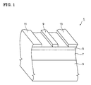
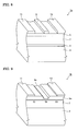
- Fig. 1 is a view representing a high electron mobility transistor according to Embodiment Mode 1.
- the high electron mobility transistor 1 includes a supporting substrate 3, an Al y Ga 1- y N epitaxial layer (0 ⁇ y ⁇ 1) 5, a GaN epitaxial layer 7, a Schottky electrode 9, a first ohmic electrode 11, and a second ohmic electrode 13.
- the supporting substrate 3 is composed of Al x Ga 1- x N (0 ⁇ x ⁇ 1), more specifically, AlN, AlGaN, or GaN.
- the Al y Ga 1- y N epitaxial layer 5 has a surface roughness (RMS) of 0.25 nm or less, and the surface roughness is defined by a square measuring 1 ⁇ m per side.
- RMS surface roughness
- the GaN epitaxial layer 7 is provided between the Al y Ga 1- y N supporting substrate 3 and the Al y Ga 1- y N epitaxial layer 5.
- the Schottky electrode 9 is provided on the Al y Ga 1- y N epitaxial layer 5.
- the first ohmic electrode 11 is provided on the Al y Ga 1- y N epitaxial layer 5.
- the second ohmic electrode 13 is provided on the Al y Ga 1- y N epitaxial layer 5.
- One of the first and second ohmic electrodes 11 and 13 constitutes a source electrode, and the other constitutes a drain electrode.
- the Schottky electrode 9 constitutes a gate electrode of the high electron mobility transistor 1.
- the inventors have found that the leakage current from the Schottky electrode 9 in contact with the Al y Ga 1- y N epitaxial layer (0 ⁇ y ⁇ 1) 5 is related to the surface roughness (RMS) of a square area measuring 1 ⁇ m per side. According to the present invention, since the surface roughness is 0.25 nm or less, the leakage current from the Schottky electrode 9 is reduced.
- Fig. 2A is a view representing the structure of the high electron mobility transistor (HEMT) according to Example.
- Fig. 2B is a view representing the structure of the HEMT according to Experiment.
- HEMT high electron mobility transistor
- a gallium nitride substrate 21 is placed in a reactor of an MOVPE device. After gases including hydrogen, nitrogen, and ammonia are supplied into the reactor, the gallium nitride substrate 21 undergoes a heat treatment. The heat treatment is performed at 1100 degrees Celsius for about 20 minutes, for example. Next, the temperature of the gallium nitride substrate 21 is increased to 1130 degrees Celsius, for example. Ammonia and trimethylgallium (TMG) are supplied into the reactor to grow a gallium nitride layer 23 of a thickness of 1.5 ⁇ m on the gallium nitride substrate 21. The gallium nitride layer 23 has a thickness of 1.5 ⁇ m, for example.
- Trimethyl aluminum (TMA), TMG, and ammonia are supplied into the reactor to grow an AlGaN layer 25 on the gallium nitride layer 23.
- the AlGaN layer 25 has a thickness of 30 nm, for example.
- an epitaxial substrate A is manufactured.
- a source electrode 27a and a drain electrode 27b of Ti/Al/Ti/Au are formed on a surface of the epitaxial substrate A, and a gate electrode 29 of Au/Ni is formed on the surface of the epitaxial substrate A.
- an HEMT-1 shown in Fig. 2A is manufactured.
- a sapphire substrate 31 is placed in the reactor of the MOVPE device. Gases including hydrogen, nitrogen, and ammonia are supplied into the reactor to heat-treat the sapphire substrate 31.
- the temperature of the heat treatment is 1170 degrees Celsius, and the heat treatment time is 10 minutes, for example.
- a seed layer 32 is grown on the sapphire substrate 31.
- a gallium nitride layer 33 and an AlGaN layer 35 are grown to manufacture an epitaxial substrate B.
- a source electrode 37a and a drain electrode 37b of Ti/Al/Ti/Au are formed, and a gate electrode 39 of Au/Ni is formed on the surface of the epitaxial substrate B.
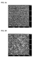
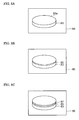
- Fig. 3A and Fig. 3B are views representing atomic force microscope (AFM) images of the surfaces of the AlGaN layers of the epitaxial substrate (sample A) and the epitaxial substrate (sample B) manufactured for the high electron mobility transistors, respectively.
- Figures show images of a square area measuring 1 ⁇ m per side.
- the sample A includes a GaN film and an AlGaN film formed on the gallium nitride substrate in this order.
- the sample B includes a seed film, a GaN film and an AlGaN film formed on the sapphire substrate in this order.
- the surface of the sample A is so flat that atomic layer steps can be observed, but the sample B has a number of grooves.
- a Schottky electrode is provided to measure the leakage current.
- An area of the Schottky electrode is 7.85 ⁇ 10 -5 cm 2 and the applied voltage is -5 volts, for example.
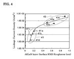
- Fig. 4 is a view of representing correspondences between the surface roughness (RMS) of the AlGaN layer and the leakage current density.
- Symbols indicated by reference marks 41a through 41d represent values obtained by measuring the structure in which the Schottky electrode is formed on the AlGaN layer that is fabricated by utilizing the gallium nitride substrate.
- Symbols indicated by reference marks 43a through 43c represent values obtained by measuring the structure in which Schottky electrode is formed on the AlGaN layer that is fabricated by utilizing the sapphire substrate.
- the supporting substrate 3 of nitride is composed of gallium nitride conductive or semi-insulating.
- the gallium nitride region is homoepitaxially grown on the gallium nitride supporting substrate.
- the carrier concentration of the gallium nitride supporting substrate is 1x10 19 cm -3 or less.
- the GaN layer 7 has a thickness between 0.1 ⁇ m and 1000 ⁇ m, inclusive.
- the GaN layer 7 has a carrier concentration of 1 ⁇ 10 17 cm -3 or less.
- the AlGaN layer 5 has a thickness between 5 nm and 50 nm, inclusive.
- the AlGaN layer 5 has a carrier concentration of 1x10 19 cm -3 or less.
- the aluminum mole fraction y of the Al y Ga 1- y N epitaxial layer 5 is preferably 0.1 or more. If the aluminum mole fraction y is less than 0.1, the band offset becomes small and two-dimensional electron gas having enough density can not be formed at the AlGaN/GaN interface.
- the aluminum mole fraction y is preferably 0.7 or less. If the aluminum mole fraction y is more than 0.7, it is highly likely that cracks are generated in the AlGaN layer. The generation of the cracks prevents the two-dimensional electron gas from being formed at the AlGaN/GaN interface.
- the Al y Ga 1- y N epitaxial layer 5 preferably has a thickness of 5 nm or more. If the thickness of the Al y Ga 1- y N epitaxial layer 5 is less than 5 nm, the distortion at the AlGaN/GaN interface becomes small and the two-dimensional electron gas is not formed.
- the Al y Ga 1- y N epitaxial layer 5 preferably has a thickness of 50 nm or less. If the thickness of the Al y Ga 1- y N epitaxial layer 5 is more than 50 nm, it is highly likely that cracks are generated in the AlGaN layer. The generation of the cracks prevents the two-dimensional electron gas from being formed at the AlGaN/GaN interface.
- the Al x Ga 1- x N supporting substrate for the high electron mobility transistor 1 is preferably composed of gallium nitride. Accordingly, Group III nitride semiconductor devices are provided using a supporting substrate of a low dislocation density.
- Fig. 5A, Fig. 5B, and Fig. 5C are views representing manufacture of the epitaxial substrate according to Embodiment Mode 2.
- a gallium nitride freestanding substrate 83 having conductivity is placed in a reactor 80.
- the following crystal growth is preferably performed by MOVPE method.
- the gallium nitride freestanding substrate 83 has a carrier concentration of 1x10 19 cm -3 or less.
- a GaN epitaxial film 85 is deposited on a first surface 83a of the gallium nitride freestanding substrate 83.
- the GaN epitaxial film 85 is preferably undoped.
- the GaN epitaxial film 85 is deposited at a temperature between 600 degrees Celsius and 1200 degrees Celsius, inclusive.
- the pressure in the reactor is between 1 kPa and 120 kPa, inclusive.
- the gallium nitride epitaxial film 85 has a thickness between 0.5 ⁇ m and 1000 ⁇ m, inclusive.
- the GaN epitaxial film 85 has a carrier concentration of 1 ⁇ 10 17 cm -3 or less. If necessary, in advance of the growth of the GaN epitaxial film 85, a buffer layer can be grown.
- the buffer layer may be composed of any of AlN, GaN, AlGaN, InGaN, and AlInGaN.
- the buffer layer restrains defects or impurities of the gallium nitride freestanding substrate 83 from affecting the GaN epitaxial layer 85, so that quality of the GaN epitaxial layer 85 can be improved.
- TMA, TMG and NH 3 are supplied to deposit an undoped or n-type AlGaN epitaxial film 87 onto the undoped GaN epitaxial film 85.
- the AlGaN epitaxial film 87 is deposited at a temperature between 600 degrees Celsius and 1200 degrees Celsius, inclusive.
- the pressure in the reactor is between 1 kPa and 120 kPa, inclusive.
- the aluminum composition of the AlGaN epitaxial film 87 is between 0.1 and 0.7, inclusive.
- the AlGaN epitaxial film 87 has a thickness of 5 nm and 50 nm, inclusive.
- the AlGaN epitaxial film 87 has a carrier concentration of 1 ⁇ 10 19 cm -3 or less. Accordingly, an epitaxial substrate 81 is obtained. By making use of this substrate, an HEMT according to Embodiment Mode 1 can be manufactured.
- the inventors have found that the leakage current from the Schottky electrode in contact with the Al y Ga 1- y N epitaxial film 87 (0 ⁇ y ⁇ 1) is related to the surface roughness (RMS) measured using the atomic force microscope. Since the square area measuring 1 ⁇ m per side is sufficiently larger for surface structures of the epitaxial layer such as atomic layer steps or grooves, it is possible to use the surface roughness (RMS) in a square area measuring 1 ⁇ m per side to indicate flatness of the surface of the epitaxial layer.
- RMS surface roughness
- the forward current in the gate electrode of the HEMT is about 1 A/cm 2 , therefore it is necessary to keep the leakage current 1 ⁇ 10 -4 A/cm 2 or less, i.e., 1/100000 or less of the forward current.
- the leakage current can be 1 ⁇ 10 -4 A/cm 2 or less.
- a Schottky electrode film for a gate electrode and the ohmic electrode films for a source electrode and a drain electrode are deposited.
- the Schottky electrode and ohmic electrodes are formed from the Schottky electrode film and the ohmic electrode films, respectively. It is possible to thin a portion of AlGaN epitaxial film 87 immediately under the Schottky electrode, and to form the Schottky electrode on the portion. This makes it possible to lower the source resistance, improve the mutual conductance, and carry out the normally off.
- n-type dopant can be added to form an n-type semiconductor region immediately under the source electrode and the drain electrode.
- an n-type semiconductor regions to which the n-type dopant is added may be grown as a contact layer on the surface of the AlGaN epitaxial film 87, and the source electrode and/or the drain electrode may be formed on the contact layer. Accordingly, the contact resistance can be reduced. Furthermore, a portion of the AlGaN layer can be thinned, and the source and/or the drain electrode can be formed on the thinned portion. Accordingly, the contact resistance can be reduced. Or the source and/or drain electrode can be formed to be in contact with the GaN layer, which has a band gap smaller than that of AlGaN, by removing the AlGaN layer. Accordingly, the contact resistance can be reduced.
- the surface roughness of the AlGaN region is used to indicate the crystal quality to monitor the quality of AlGaN film with which the Schottky electrode constitutes a Schottky junction, so that an epitaxial substrate can be provided for a semiconductor device in which a backward leak current that flows through the Schottky junction when a voltage is applied across the Schottky electrode and the ohmic electrode can be reduced.
- Fig. 6 is a view representing one example of locations of high dislocation regions and low dislocation regions in a gallium nitride freestanding substrate for Embodiment Modes 1 and 2.
- a first surface 82a of the gallium nitride freestanding substrate 82 for the epitaxial substrate 81 includes first areas where high dislocation regions 82c having a relatively large screw dislocation density appear, and a second area where a low dislocation region 82d having a relatively small screw dislocation density appears.
- the high dislocation regions 82c are surrounded by the low dislocation region 82d, and the first areas are randomly distributed in a dot-like pattern in the second area on the first surface 82a.
- the screw dislocation density is 1 ⁇ 10 8 cm -2 or less, for example.
- the epitaxial substrate 81 gives an epitaxial layer having a lowered dislocation density in the low dislocation region 82d. Consequently, the backward leak current is reduced and the backward breakdown voltage is improved.
- Fig. 7 is a view representing another example of locations of the high dislocation regions and the low dislocation regions in a gallium nitride freestanding substrate for Embodiment Modes 1 and 2.
- a first surface 84a of the gallium nitride freestanding substrate 84 for the epitaxial substrate 81 includes first areas where high dislocation regions 84c having a relatively large screw dislocation density appear, and second areas where low dislocation regions 84d having a relatively small screw dislocation density appear.
- the high dislocation regions 84c are surrounded by the low dislocation regions 84d, and the first areas are distributed in a striped pattern in the second area on the first surface 84a.
- the screw dislocation density is 1 ⁇ 10 8 cm -2 or less, for example.
- the epitaxial substrate 81 gives an epitaxial layer having a lowered dislocation density in the low dislocation regions 84d. Accordingly, the backward leak current is decreased, and the backward breakdown voltage is improved.
- the Al x Ga 1- x N (0 ⁇ x ⁇ 1) substrate can be used as a freestanding substrate. More specifically, the freestanding substrate can be composed of AlN, AlGaN or GaN.
- Fig. 8 is a view representing the high electron mobility transistor according to one modification of Embodiment Mode 1.
- an additional gallium nitride semiconductor layer 4 can be provided between the GaN epitaxial layer 7 and the gallium nitride supporting substrate 13.
- the gallium nitride semiconductor layer 4 is composed of AlN, GaN, AlGaN, InGaN, or AlInGaN, for example.
- the gallium nitride semiconductor layer 4 restrains the affect of defects of and impurities on the supporting substrate from propagating to the upper layers, thereby improving the quality of the GaN epitaxial layer 7.
- Fig. 9 is a view representing the high electron mobility transistor according to other modification of Embodiment Mode 1.
- a high electron mobility transistor 1b can be provided with an AlGaN layer 5a in place of the AlGaN layer 5 of the high electron mobility transistor 1a.
- the AlGaN layer 5a includes a first portion 5b, a second portion 5c and a third portion 5d.
- the first portion 5b is positioned between the second portion 5c and the third portion 5d.
- the thickens of the first portion 5b is smaller than that of the second portion 5c and that of the third portion 5d, thereby forming a recess structure in the AlGaN layer 5a.
- a gate electrode 9a is provided on the first portion 5b.
- the recess structure is formed by thinning the Al y Ga 1- y N epitaxial layer 15 by etching.
- the recess gate structure makes it possible to reduce the source resistance, improve the mutual conductance, and perform a normally off.
- Fig. 10 is a view representing the high electron mobility transistor according to other modification of Embodiment Mode 1.
- a high electron mobility transistor 1c can be provided with, in place of the AlGaN layer 5 of the high electron mobility transistor 1a, an AlGaN layer 5e.
- the AlGaN layer 5e includes a first portion 5f, a second portion 5g, and a third portion 5h.
- the first portion 5f is positioned between the second portion 5g and the third portion 5h.
- the thickness of the first portion 5f is larger than that of the second portion 5g and that of the third portion 5h, thereby forming a recess structure in the AlGaN layer 5e.
- the recess structure is formed by thinning the Al y Ga 1- y N epitaxial layer 15 by etching.
- a source electrode 11a is provided on the second portion 5g.
- a drain electrode 13a is provided on the third portion 5h.
- the recess ohmic structure can reduce the contact resistance.
- Fig. 11 is a view representing the high electron mobility transistor according to other modification of Embodiment Mode 1.
- a high electron mobility transistor 1d may be further provided with contact layers 6 on the AlGaN layer 5 of the high electron mobility transistor 1a for a source electrode and a drain electrode.
- the contact layers 6 can be composed of gallium nitride semiconductors such as GaN, InN, and InGaN.
- the band gap of the contact layer 6 is preferably smaller than that of the AlGaN layer 5.
- the carrier concentration of the contact layer 6 is preferably larger than that of the AlGaN layer 5.
- the gate electrode 9 constitutes a Schottky junction with the AlGaN layer 5, and a source electrode 11b and a drain electrode 13b constitute ohmic contacts with contact layers 6.
- the contact layers 6 are positioned between the source electrode 11b and the AlGaN layer 5, and between the drain electrode 13b and the AlGaN layer 5.
- the contact layer added structure can also reduce the contact resistance.
Landscapes
- Junction Field-Effect Transistors (AREA)
Applications Claiming Priority (3)
| Application Number | Priority Date | Filing Date | Title |
|---|---|---|---|
| JP2005073519 | 2005-03-15 | ||
| JP2006019502A JP2006295126A (ja) | 2005-03-15 | 2006-01-27 | Iii族窒化物半導体素子およびエピタキシャル基板 |
| PCT/JP2006/304095 WO2006098167A1 (ja) | 2005-03-15 | 2006-03-03 | Iii族窒化物半導体素子およびエピタキシャル基板 |
Publications (3)
| Publication Number | Publication Date |
|---|---|
| EP1746641A1 true EP1746641A1 (de) | 2007-01-24 |
| EP1746641A4 EP1746641A4 (de) | 2009-07-08 |
| EP1746641B1 EP1746641B1 (de) | 2011-08-24 |
Family
ID=36991515
Family Applications (1)
| Application Number | Title | Priority Date | Filing Date |
|---|---|---|---|
| EP06715178A Expired - Lifetime EP1746641B1 (de) | 2005-03-15 | 2006-03-03 | Herstellungsverfahren für ein Gruppe III-Nitrid-Halbleiterbauelement und epitaktisches Substrat |
Country Status (7)
| Country | Link |
|---|---|
| US (1) | US20080265258A1 (de) |
| EP (1) | EP1746641B1 (de) |
| JP (1) | JP2006295126A (de) |
| KR (1) | KR20070113093A (de) |
| CA (1) | CA2564423A1 (de) |
| TW (1) | TW200731352A (de) |
| WO (1) | WO2006098167A1 (de) |
Cited By (2)
| Publication number | Priority date | Publication date | Assignee | Title |
|---|---|---|---|---|
| WO2009123936A3 (en) * | 2008-03-31 | 2009-12-30 | Bridgelux, Inc. | Light emitting diodes with smooth surface for reflective electrode |
| EP2211376A4 (de) * | 2007-11-02 | 2012-04-04 | Sumitomo Electric Industries | Iii-nitridelektronikbauelement und iii-nitridhalbleiterepitaxialsubstrat |
Families Citing this family (15)
| Publication number | Priority date | Publication date | Assignee | Title |
|---|---|---|---|---|
| CA2483403A1 (en) * | 2002-04-30 | 2003-11-13 | Jeffrey S. Flynn | High voltage switching devices and process for forming same |
| RU2316076C1 (ru) * | 2006-11-14 | 2008-01-27 | Закрытое Акционерное Общество "Светлана-Рост" | Полупроводниковая гетероструктура полевого транзистора |
| US20100072518A1 (en) * | 2008-09-12 | 2010-03-25 | Georgia Tech Research Corporation | Semiconductor devices and methods of fabricating same |
| JP5564842B2 (ja) | 2009-07-10 | 2014-08-06 | サンケン電気株式会社 | 半導体装置 |
| JP2010045416A (ja) * | 2009-11-25 | 2010-02-25 | Sumitomo Electric Ind Ltd | Iii族窒化物電子デバイス |
| WO2014024310A1 (ja) * | 2012-08-10 | 2014-02-13 | 日本碍子株式会社 | 半導体素子、hemt素子、および半導体素子の製造方法 |
| JP6275817B2 (ja) * | 2013-03-15 | 2018-02-07 | クリスタル アイエス, インコーポレーテッドCrystal Is, Inc. | 仮像電子及び光学電子装置に対する平面コンタクト |
| EP3426147B1 (de) * | 2016-03-10 | 2020-06-17 | Epitronic Holdings Pte. Ltd. | Mikroelektronischer sensor für darmdiagnostika und überwachung der darmtätigkeit |
| US10932684B2 (en) * | 2016-03-10 | 2021-03-02 | Epitronic Holdings Pte Ltd. | Microelectronic sensor for air quality monitoring |
| US10945643B2 (en) * | 2016-03-10 | 2021-03-16 | Epitronic Holdings Pte. Ltd. | Microelectronic sensor for biometric authentication |
| CN109414175B (zh) * | 2016-03-10 | 2021-10-22 | 艾皮乔尼克控股有限公司 | 用于生理参数的非侵入式监测的微电子传感器 |
| US11000203B2 (en) * | 2016-03-10 | 2021-05-11 | Epitronic Holdings Pte Ltd. | Microelectronic sensor for intestinal and gut diagnostics and gut motility monitoring |
| EP3457916A1 (de) * | 2016-05-17 | 2019-03-27 | Epitronic Holdings Pte. Ltd. | Mikroelektronischer sensor zur biometrischen authentifizierung |
| US9865721B1 (en) * | 2016-06-15 | 2018-01-09 | Qorvo Us, Inc. | High electron mobility transistor (HEMT) device and method of making the same |
| US10720902B2 (en) * | 2016-08-16 | 2020-07-21 | Epitronic Holdings Pte. Ltd | Surface acoustic wave RFID sensor for chemical detection and (bio)molecular diagnostics |
Family Cites Families (11)
| Publication number | Priority date | Publication date | Assignee | Title |
|---|---|---|---|---|
| US6586781B2 (en) * | 2000-02-04 | 2003-07-01 | Cree Lighting Company | Group III nitride based FETs and HEMTs with reduced trapping and method for producing the same |
| JP2002289528A (ja) * | 2001-03-23 | 2002-10-04 | Yasuhiko Arakawa | 窒化ガリウム系化合物半導体の結晶成長法、および窒化ガリウム系化合物半導体を備えた電子デバイス |
| US7501023B2 (en) * | 2001-07-06 | 2009-03-10 | Technologies And Devices, International, Inc. | Method and apparatus for fabricating crack-free Group III nitride semiconductor materials |
| JP4906023B2 (ja) * | 2001-08-14 | 2012-03-28 | 古河電気工業株式会社 | GaN系半導体装置 |
| JP2003234356A (ja) * | 2002-02-07 | 2003-08-22 | Oki Electric Ind Co Ltd | 高電子移動度トランジスタ |
| JP3977659B2 (ja) * | 2002-02-21 | 2007-09-19 | 沖電気工業株式会社 | ヘテロ接合電界効果トランジスタ |
| US8089097B2 (en) * | 2002-12-27 | 2012-01-03 | Momentive Performance Materials Inc. | Homoepitaxial gallium-nitride-based electronic devices and method for producing same |
| WO2004061923A1 (en) * | 2002-12-27 | 2004-07-22 | General Electric Company | Gallium nitride crystal, homoepitaxial gallium-nitride-based devices and method for producing same |
| JP4179539B2 (ja) * | 2003-01-15 | 2008-11-12 | 富士通株式会社 | 化合物半導体装置及びその製造方法 |
| JP2004327882A (ja) * | 2003-04-28 | 2004-11-18 | Ngk Insulators Ltd | エピタキシャル基板、半導体素子および高電子移動度トランジスタ |
| US20050139838A1 (en) * | 2003-12-26 | 2005-06-30 | Matsushita Electric Industrial Co., Ltd. | Semiconductor device and method for manufacturing semiconductor device |
-
2006
- 2006-01-27 JP JP2006019502A patent/JP2006295126A/ja active Pending
- 2006-03-03 WO PCT/JP2006/304095 patent/WO2006098167A1/ja not_active Ceased
- 2006-03-03 CA CA002564423A patent/CA2564423A1/en not_active Abandoned
- 2006-03-03 EP EP06715178A patent/EP1746641B1/de not_active Expired - Lifetime
- 2006-03-03 KR KR1020067023823A patent/KR20070113093A/ko not_active Withdrawn
- 2006-03-03 US US11/569,066 patent/US20080265258A1/en not_active Abandoned
- 2006-03-10 TW TW095108062A patent/TW200731352A/zh unknown
Cited By (9)
| Publication number | Priority date | Publication date | Assignee | Title |
|---|---|---|---|---|
| EP2211376A4 (de) * | 2007-11-02 | 2012-04-04 | Sumitomo Electric Industries | Iii-nitridelektronikbauelement und iii-nitridhalbleiterepitaxialsubstrat |
| US8541816B2 (en) | 2007-11-02 | 2013-09-24 | Sumitomo Electric Industries, Ltd. | III nitride electronic device and III nitride semiconductor epitaxial substrate |
| WO2009123936A3 (en) * | 2008-03-31 | 2009-12-30 | Bridgelux, Inc. | Light emitting diodes with smooth surface for reflective electrode |
| US7781780B2 (en) | 2008-03-31 | 2010-08-24 | Bridgelux, Inc. | Light emitting diodes with smooth surface for reflective electrode |
| CN102150272A (zh) * | 2008-03-31 | 2011-08-10 | 普瑞光电股份有限公司 | 具供设置反射性电极的平滑表面的发光二极管 |
| US8163578B2 (en) | 2008-03-31 | 2012-04-24 | Bridgelux, Inc. | Light emitting diodes with smooth surface for reflective electrode |
| US8168984B2 (en) | 2008-03-31 | 2012-05-01 | Bridgelux, Inc. | Light emitting diodes with smooth surface for reflective electrode |
| CN102150272B (zh) * | 2008-03-31 | 2015-03-11 | 马帝斯Ip股份有限公司 | 具供设置反射性电极的平滑表面的发光二极管 |
| US9437776B2 (en) | 2008-03-31 | 2016-09-06 | Toshiba Corporation | Method for manufacturing light emitting diodes with smooth surface for reflective electrode |
Also Published As
| Publication number | Publication date |
|---|---|
| WO2006098167A1 (ja) | 2006-09-21 |
| JP2006295126A (ja) | 2006-10-26 |
| KR20070113093A (ko) | 2007-11-28 |
| US20080265258A1 (en) | 2008-10-30 |
| EP1746641B1 (de) | 2011-08-24 |
| TW200731352A (en) | 2007-08-16 |
| CA2564423A1 (en) | 2006-09-21 |
| EP1746641A4 (de) | 2009-07-08 |
Similar Documents
| Publication | Publication Date | Title |
|---|---|---|
| EP1746641A1 (de) | Gruppe iii-nitrid-halbleiterbauelement und epitaktisches substrat | |
| US10580646B2 (en) | Epitaxial substrate for semiconductor elements, semiconductor element, and manufacturing method for epitaxial substrates for semiconductor elements | |
| US8653561B2 (en) | III-nitride semiconductor electronic device, and method of fabricating III-nitride semiconductor electronic device | |
| CN101842884B (zh) | Ⅲ族氮化物电子器件及ⅲ族氮化物半导体外延衬底 | |
| JP3960957B2 (ja) | 半導体電子デバイス | |
| JP5465469B2 (ja) | エピタキシャル基板、半導体デバイス基板、およびhemt素子 | |
| EP1777737A1 (de) | Transistor mit hoher elektronenmobilität, feldeffekt-transistor, epitaxiales substrat, verfahren zur herstellung des epitaxialen substrats und verfahren zur herstellung eines gruppe-iii-nitrid-transistors | |
| US11430875B2 (en) | Method for manufacturing transistor | |
| EP2251464B1 (de) | Epitaxiesubstrat für Halbleiterbauelement, Halbleiterbauelement und Verfahren zur Herstellung eines Epitaxiesubstrats für ein Halbleiterbauelement | |
| US20100301393A1 (en) | Field effect transistor and manufacturing method therefor | |
| US20240363745A1 (en) | High-frequency group iii-nitride-based high electron mobility transistors with high-aluminum concentration barriers and recessed gates | |
| US9401402B2 (en) | Nitride semiconductor device and nitride semiconductor substrate | |
| EP1876649A1 (de) | Gruppe iii-nitrid-halbleiterbauelement und epitaktisches substrat | |
| US20110049573A1 (en) | Group iii nitride semiconductor wafer and group iii nitride semiconductor device | |
| JP5378128B2 (ja) | 電子デバイス用エピタキシャル基板およびiii族窒化物電子デバイス用エピタキシャル基板 | |
| US8410524B2 (en) | Group III nitride semiconductor device and epitaxial substrate | |
| US20240136180A1 (en) | Diamond-Capped Gallium Oxide Transistor | |
| JP2009246307A (ja) | 半導体装置及びその製造方法 | |
| JP4972879B2 (ja) | 電界効果トランジスタ、半導体素子、及びエピタキシャル基板 | |
| Mamun | Thermal Management of Power Electronic Devices Using Single Crystal Aln Heat Spreaders | |
| CN1977367A (zh) | Ⅲ族氮化物半导体器件和外延衬底 | |
| CN121419274A (zh) | 一种高电子迁移率晶体管的外延层及钝化层制备方法 | |
| Park et al. | GaN power switching device growth by plasma assisted molecular beam epitaxy | |
| Xie et al. | AlGaN/GaN MODFET regrown by rf-MBE on MOCVD templates |
Legal Events
| Date | Code | Title | Description |
|---|---|---|---|
| PUAI | Public reference made under article 153(3) epc to a published international application that has entered the european phase |
Free format text: ORIGINAL CODE: 0009012 |
|
| 17P | Request for examination filed |
Effective date: 20061108 |
|
| AK | Designated contracting states |
Kind code of ref document: A1 Designated state(s): AT BE BG CH CY CZ DE DK EE ES FI FR GB GR HU IE IS IT LI LT LU LV MC NL PL PT RO SE SI SK TR |
|
| AX | Request for extension of the european patent |
Extension state: AL BA HR MK YU |
|
| DAX | Request for extension of the european patent (deleted) | ||
| RBV | Designated contracting states (corrected) |
Designated state(s): DE FR GB NL |
|
| A4 | Supplementary search report drawn up and despatched |
Effective date: 20090605 |
|
| 17Q | First examination report despatched |
Effective date: 20100201 |
|
| GRAP | Despatch of communication of intention to grant a patent |
Free format text: ORIGINAL CODE: EPIDOSNIGR1 |
|
| RTI1 | Title (correction) |
Free format text: METHOD OF MANUFACTURING A GROUP III NITRIDE SEMICONDUCTOR DEVICE AND EPITAXIAL SUBSTRATE |
|
| GRAS | Grant fee paid |
Free format text: ORIGINAL CODE: EPIDOSNIGR3 |
|
| GRAA | (expected) grant |
Free format text: ORIGINAL CODE: 0009210 |
|
| AK | Designated contracting states |
Kind code of ref document: B1 Designated state(s): DE FR GB NL |
|
| REG | Reference to a national code |
Ref country code: GB Ref legal event code: FG4D |
|
| REG | Reference to a national code |
Ref country code: DE Ref legal event code: R096 Ref document number: 602006023993 Country of ref document: DE Effective date: 20111020 |
|
| REG | Reference to a national code |
Ref country code: NL Ref legal event code: VDEP Effective date: 20110824 |
|
| PG25 | Lapsed in a contracting state [announced via postgrant information from national office to epo] |
Ref country code: NL Free format text: LAPSE BECAUSE OF FAILURE TO SUBMIT A TRANSLATION OF THE DESCRIPTION OR TO PAY THE FEE WITHIN THE PRESCRIBED TIME-LIMIT Effective date: 20110824 |
|
| PGFP | Annual fee paid to national office [announced via postgrant information from national office to epo] |
Ref country code: FR Payment date: 20120319 Year of fee payment: 7 |
|
| PGFP | Annual fee paid to national office [announced via postgrant information from national office to epo] |
Ref country code: GB Payment date: 20120301 Year of fee payment: 7 |
|
| PLBE | No opposition filed within time limit |
Free format text: ORIGINAL CODE: 0009261 |
|
| STAA | Information on the status of an ep patent application or granted ep patent |
Free format text: STATUS: NO OPPOSITION FILED WITHIN TIME LIMIT |
|
| PGFP | Annual fee paid to national office [announced via postgrant information from national office to epo] |
Ref country code: DE Payment date: 20120404 Year of fee payment: 7 |
|
| 26N | No opposition filed |
Effective date: 20120525 |
|
| REG | Reference to a national code |
Ref country code: DE Ref legal event code: R097 Ref document number: 602006023993 Country of ref document: DE Effective date: 20120525 |
|
| GBPC | Gb: european patent ceased through non-payment of renewal fee |
Effective date: 20130303 |
|
| REG | Reference to a national code |
Ref country code: FR Ref legal event code: ST Effective date: 20131129 |
|
| REG | Reference to a national code |
Ref country code: DE Ref legal event code: R119 Ref document number: 602006023993 Country of ref document: DE Effective date: 20131001 |
|
| PG25 | Lapsed in a contracting state [announced via postgrant information from national office to epo] |
Ref country code: DE Free format text: LAPSE BECAUSE OF NON-PAYMENT OF DUE FEES Effective date: 20131001 Ref country code: GB Free format text: LAPSE BECAUSE OF NON-PAYMENT OF DUE FEES Effective date: 20130303 Ref country code: FR Free format text: LAPSE BECAUSE OF NON-PAYMENT OF DUE FEES Effective date: 20130402 |