EP1737282A1 - Circuit board, its manufacturing method, and joint box using circuit board - Google Patents
Circuit board, its manufacturing method, and joint box using circuit board Download PDFInfo
- Publication number
- EP1737282A1 EP1737282A1 EP05727833A EP05727833A EP1737282A1 EP 1737282 A1 EP1737282 A1 EP 1737282A1 EP 05727833 A EP05727833 A EP 05727833A EP 05727833 A EP05727833 A EP 05727833A EP 1737282 A1 EP1737282 A1 EP 1737282A1
- Authority
- EP
- European Patent Office
- Prior art keywords
- circuit
- resin plate
- foil
- circuit board
- terminals
- Prior art date
- Legal status (The legal status is an assumption and is not a legal conclusion. Google has not performed a legal analysis and makes no representation as to the accuracy of the status listed.)
- Withdrawn
Links
Images






Classifications
-
- H—ELECTRICITY
- H05—ELECTRIC TECHNIQUES NOT OTHERWISE PROVIDED FOR
- H05K—PRINTED CIRCUITS; CASINGS OR CONSTRUCTIONAL DETAILS OF ELECTRIC APPARATUS; MANUFACTURE OF ASSEMBLAGES OF ELECTRICAL COMPONENTS
- H05K3/00—Apparatus or processes for manufacturing printed circuits
- H05K3/10—Apparatus or processes for manufacturing printed circuits in which conductive material is applied to the insulating support in such a manner as to form the desired conductive pattern
- H05K3/20—Apparatus or processes for manufacturing printed circuits in which conductive material is applied to the insulating support in such a manner as to form the desired conductive pattern by affixing prefabricated conductor pattern
- H05K3/202—Apparatus or processes for manufacturing printed circuits in which conductive material is applied to the insulating support in such a manner as to form the desired conductive pattern by affixing prefabricated conductor pattern using self-supporting metal foil pattern
-
- H—ELECTRICITY
- H02—GENERATION; CONVERSION OR DISTRIBUTION OF ELECTRIC POWER
- H02G—INSTALLATION OF ELECTRIC CABLES OR LINES, OR OF COMBINED OPTICAL AND ELECTRIC CABLES OR LINES
- H02G3/00—Installations of electric cables or lines or protective tubing therefor in or on buildings, equivalent structures or vehicles
- H02G3/02—Details
- H02G3/08—Distribution boxes; Connection or junction boxes
-
- H—ELECTRICITY
- H01—ELECTRIC ELEMENTS
- H01R—ELECTRICALLY-CONDUCTIVE CONNECTIONS; STRUCTURAL ASSOCIATIONS OF A PLURALITY OF MUTUALLY-INSULATED ELECTRICAL CONNECTING ELEMENTS; COUPLING DEVICES; CURRENT COLLECTORS
- H01R12/00—Structural associations of a plurality of mutually-insulated electrical connecting elements, specially adapted for printed circuits, e.g. printed circuit boards [PCB], flat or ribbon cables, or like generally planar structures, e.g. terminal strips, terminal blocks; Coupling devices specially adapted for printed circuits, flat or ribbon cables, or like generally planar structures; Terminals specially adapted for contact with, or insertion into, printed circuits, flat or ribbon cables, or like generally planar structures
- H01R12/50—Fixed connections
- H01R12/51—Fixed connections for rigid printed circuits or like structures
- H01R12/52—Fixed connections for rigid printed circuits or like structures connecting to other rigid printed circuits or like structures
- H01R12/523—Fixed connections for rigid printed circuits or like structures connecting to other rigid printed circuits or like structures by an interconnection through aligned holes in the boards or multilayer board
-
- H—ELECTRICITY
- H01—ELECTRIC ELEMENTS
- H01R—ELECTRICALLY-CONDUCTIVE CONNECTIONS; STRUCTURAL ASSOCIATIONS OF A PLURALITY OF MUTUALLY-INSULATED ELECTRICAL CONNECTING ELEMENTS; COUPLING DEVICES; CURRENT COLLECTORS
- H01R9/00—Structural associations of a plurality of mutually-insulated electrical connecting elements, e.g. terminal strips or terminal blocks; Terminals or binding posts mounted upon a base or in a case; Bases therefor
- H01R9/22—Bases, e.g. strip, block, panel
- H01R9/24—Terminal blocks
- H01R9/2458—Electrical interconnections between terminal blocks
- H01R9/2466—Electrical interconnections between terminal blocks using a planar conductive structure, e.g. printed circuit board
-
- H—ELECTRICITY
- H02—GENERATION; CONVERSION OR DISTRIBUTION OF ELECTRIC POWER
- H02G—INSTALLATION OF ELECTRIC CABLES OR LINES, OR OF COMBINED OPTICAL AND ELECTRIC CABLES OR LINES
- H02G3/00—Installations of electric cables or lines or protective tubing therefor in or on buildings, equivalent structures or vehicles
- H02G3/02—Details
- H02G3/08—Distribution boxes; Connection or junction boxes
- H02G3/16—Distribution boxes; Connection or junction boxes structurally associated with support for line-connecting terminals within the box
-
- H—ELECTRICITY
- H05—ELECTRIC TECHNIQUES NOT OTHERWISE PROVIDED FOR
- H05K—PRINTED CIRCUITS; CASINGS OR CONSTRUCTIONAL DETAILS OF ELECTRIC APPARATUS; MANUFACTURE OF ASSEMBLAGES OF ELECTRICAL COMPONENTS
- H05K1/00—Printed circuits
- H05K1/02—Details
-
- H—ELECTRICITY
- H05—ELECTRIC TECHNIQUES NOT OTHERWISE PROVIDED FOR
- H05K—PRINTED CIRCUITS; CASINGS OR CONSTRUCTIONAL DETAILS OF ELECTRIC APPARATUS; MANUFACTURE OF ASSEMBLAGES OF ELECTRICAL COMPONENTS
- H05K13/00—Apparatus or processes specially adapted for manufacturing or adjusting assemblages of electric components
- H05K13/0061—Tools for holding the circuit boards during processing; handling transport of printed circuit boards
-
- H—ELECTRICITY
- H05—ELECTRIC TECHNIQUES NOT OTHERWISE PROVIDED FOR
- H05K—PRINTED CIRCUITS; CASINGS OR CONSTRUCTIONAL DETAILS OF ELECTRIC APPARATUS; MANUFACTURE OF ASSEMBLAGES OF ELECTRICAL COMPONENTS
- H05K3/00—Apparatus or processes for manufacturing printed circuits
- H05K3/02—Apparatus or processes for manufacturing printed circuits in which the conductive material is applied to the surface of the insulating support and is thereafter removed from such areas of the surface which are not intended for current conducting or shielding
- H05K3/04—Apparatus or processes for manufacturing printed circuits in which the conductive material is applied to the surface of the insulating support and is thereafter removed from such areas of the surface which are not intended for current conducting or shielding the conductive material being removed mechanically, e.g. by punching
- H05K3/041—Apparatus or processes for manufacturing printed circuits in which the conductive material is applied to the surface of the insulating support and is thereafter removed from such areas of the surface which are not intended for current conducting or shielding the conductive material being removed mechanically, e.g. by punching by using a die for cutting the conductive material
-
- H—ELECTRICITY
- H05—ELECTRIC TECHNIQUES NOT OTHERWISE PROVIDED FOR
- H05K—PRINTED CIRCUITS; CASINGS OR CONSTRUCTIONAL DETAILS OF ELECTRIC APPARATUS; MANUFACTURE OF ASSEMBLAGES OF ELECTRICAL COMPONENTS
- H05K3/00—Apparatus or processes for manufacturing printed circuits
- H05K3/10—Apparatus or processes for manufacturing printed circuits in which conductive material is applied to the insulating support in such a manner as to form the desired conductive pattern
- H05K3/20—Apparatus or processes for manufacturing printed circuits in which conductive material is applied to the insulating support in such a manner as to form the desired conductive pattern by affixing prefabricated conductor pattern
-
- H—ELECTRICITY
- H05—ELECTRIC TECHNIQUES NOT OTHERWISE PROVIDED FOR
- H05K—PRINTED CIRCUITS; CASINGS OR CONSTRUCTIONAL DETAILS OF ELECTRIC APPARATUS; MANUFACTURE OF ASSEMBLAGES OF ELECTRICAL COMPONENTS
- H05K2201/00—Indexing scheme relating to printed circuits covered by H05K1/00
- H05K2201/03—Conductive materials
- H05K2201/0332—Structure of the conductor
- H05K2201/0364—Conductor shape
- H05K2201/0376—Flush conductors, i.e. flush with the surface of the printed circuit
-
- H—ELECTRICITY
- H05—ELECTRIC TECHNIQUES NOT OTHERWISE PROVIDED FOR
- H05K—PRINTED CIRCUITS; CASINGS OR CONSTRUCTIONAL DETAILS OF ELECTRIC APPARATUS; MANUFACTURE OF ASSEMBLAGES OF ELECTRICAL COMPONENTS
- H05K2201/00—Indexing scheme relating to printed circuits covered by H05K1/00
- H05K2201/03—Conductive materials
- H05K2201/0332—Structure of the conductor
- H05K2201/0388—Other aspects of conductors
- H05K2201/0394—Conductor crossing over a hole in the substrate or a gap between two separate substrate parts
-
- H—ELECTRICITY
- H05—ELECTRIC TECHNIQUES NOT OTHERWISE PROVIDED FOR
- H05K—PRINTED CIRCUITS; CASINGS OR CONSTRUCTIONAL DETAILS OF ELECTRIC APPARATUS; MANUFACTURE OF ASSEMBLAGES OF ELECTRICAL COMPONENTS
- H05K2201/00—Indexing scheme relating to printed circuits covered by H05K1/00
- H05K2201/03—Conductive materials
- H05K2201/0332—Structure of the conductor
- H05K2201/0388—Other aspects of conductors
- H05K2201/0397—Tab
-
- H—ELECTRICITY
- H05—ELECTRIC TECHNIQUES NOT OTHERWISE PROVIDED FOR
- H05K—PRINTED CIRCUITS; CASINGS OR CONSTRUCTIONAL DETAILS OF ELECTRIC APPARATUS; MANUFACTURE OF ASSEMBLAGES OF ELECTRICAL COMPONENTS
- H05K2201/00—Indexing scheme relating to printed circuits covered by H05K1/00
- H05K2201/09—Shape and layout
- H05K2201/09009—Substrate related
- H05K2201/09036—Recesses or grooves in insulating substrate
-
- H—ELECTRICITY
- H05—ELECTRIC TECHNIQUES NOT OTHERWISE PROVIDED FOR
- H05K—PRINTED CIRCUITS; CASINGS OR CONSTRUCTIONAL DETAILS OF ELECTRIC APPARATUS; MANUFACTURE OF ASSEMBLAGES OF ELECTRICAL COMPONENTS
- H05K2201/00—Indexing scheme relating to printed circuits covered by H05K1/00
- H05K2201/09—Shape and layout
- H05K2201/09009—Substrate related
- H05K2201/09045—Locally raised area or protrusion of insulating substrate
-
- H—ELECTRICITY
- H05—ELECTRIC TECHNIQUES NOT OTHERWISE PROVIDED FOR
- H05K—PRINTED CIRCUITS; CASINGS OR CONSTRUCTIONAL DETAILS OF ELECTRIC APPARATUS; MANUFACTURE OF ASSEMBLAGES OF ELECTRICAL COMPONENTS
- H05K2201/00—Indexing scheme relating to printed circuits covered by H05K1/00
- H05K2201/09—Shape and layout
- H05K2201/09009—Substrate related
- H05K2201/091—Locally and permanently deformed areas including dielectric material
-
- H—ELECTRICITY
- H05—ELECTRIC TECHNIQUES NOT OTHERWISE PROVIDED FOR
- H05K—PRINTED CIRCUITS; CASINGS OR CONSTRUCTIONAL DETAILS OF ELECTRIC APPARATUS; MANUFACTURE OF ASSEMBLAGES OF ELECTRICAL COMPONENTS
- H05K2201/00—Indexing scheme relating to printed circuits covered by H05K1/00
- H05K2201/09—Shape and layout
- H05K2201/09209—Shape and layout details of conductors
- H05K2201/095—Conductive through-holes or vias
- H05K2201/096—Vertically aligned vias, holes or stacked vias
-
- H—ELECTRICITY
- H05—ELECTRIC TECHNIQUES NOT OTHERWISE PROVIDED FOR
- H05K—PRINTED CIRCUITS; CASINGS OR CONSTRUCTIONAL DETAILS OF ELECTRIC APPARATUS; MANUFACTURE OF ASSEMBLAGES OF ELECTRICAL COMPONENTS
- H05K2201/00—Indexing scheme relating to printed circuits covered by H05K1/00
- H05K2201/10—Details of components or other objects attached to or integrated in a printed circuit board
- H05K2201/10227—Other objects, e.g. metallic pieces
- H05K2201/10287—Metal wires as connectors or conductors
-
- H—ELECTRICITY
- H05—ELECTRIC TECHNIQUES NOT OTHERWISE PROVIDED FOR
- H05K—PRINTED CIRCUITS; CASINGS OR CONSTRUCTIONAL DETAILS OF ELECTRIC APPARATUS; MANUFACTURE OF ASSEMBLAGES OF ELECTRICAL COMPONENTS
- H05K2201/00—Indexing scheme relating to printed circuits covered by H05K1/00
- H05K2201/10—Details of components or other objects attached to or integrated in a printed circuit board
- H05K2201/10227—Other objects, e.g. metallic pieces
- H05K2201/10401—Eyelets, i.e. rings inserted into a hole through a circuit board
-
- H—ELECTRICITY
- H05—ELECTRIC TECHNIQUES NOT OTHERWISE PROVIDED FOR
- H05K—PRINTED CIRCUITS; CASINGS OR CONSTRUCTIONAL DETAILS OF ELECTRIC APPARATUS; MANUFACTURE OF ASSEMBLAGES OF ELECTRICAL COMPONENTS
- H05K2201/00—Indexing scheme relating to printed circuits covered by H05K1/00
- H05K2201/10—Details of components or other objects attached to or integrated in a printed circuit board
- H05K2201/10431—Details of mounted components
- H05K2201/1059—Connections made by press-fit insertion
-
- H—ELECTRICITY
- H05—ELECTRIC TECHNIQUES NOT OTHERWISE PROVIDED FOR
- H05K—PRINTED CIRCUITS; CASINGS OR CONSTRUCTIONAL DETAILS OF ELECTRIC APPARATUS; MANUFACTURE OF ASSEMBLAGES OF ELECTRICAL COMPONENTS
- H05K2201/00—Indexing scheme relating to printed circuits covered by H05K1/00
- H05K2201/10—Details of components or other objects attached to or integrated in a printed circuit board
- H05K2201/10431—Details of mounted components
- H05K2201/10598—Means for fastening a component, a casing or a heat sink whereby a pressure is exerted on the component towards the PCB
-
- H—ELECTRICITY
- H05—ELECTRIC TECHNIQUES NOT OTHERWISE PROVIDED FOR
- H05K—PRINTED CIRCUITS; CASINGS OR CONSTRUCTIONAL DETAILS OF ELECTRIC APPARATUS; MANUFACTURE OF ASSEMBLAGES OF ELECTRICAL COMPONENTS
- H05K2203/00—Indexing scheme relating to apparatus or processes for manufacturing printed circuits covered by H05K3/00
- H05K2203/08—Treatments involving gases
- H05K2203/081—Blowing of gas, e.g. for cooling or for providing heat during solder reflowing
-
- H—ELECTRICITY
- H05—ELECTRIC TECHNIQUES NOT OTHERWISE PROVIDED FOR
- H05K—PRINTED CIRCUITS; CASINGS OR CONSTRUCTIONAL DETAILS OF ELECTRIC APPARATUS; MANUFACTURE OF ASSEMBLAGES OF ELECTRICAL COMPONENTS
- H05K2203/00—Indexing scheme relating to apparatus or processes for manufacturing printed circuits covered by H05K3/00
- H05K2203/08—Treatments involving gases
- H05K2203/082—Suction, e.g. for holding solder balls or components
-
- H—ELECTRICITY
- H05—ELECTRIC TECHNIQUES NOT OTHERWISE PROVIDED FOR
- H05K—PRINTED CIRCUITS; CASINGS OR CONSTRUCTIONAL DETAILS OF ELECTRIC APPARATUS; MANUFACTURE OF ASSEMBLAGES OF ELECTRICAL COMPONENTS
- H05K2203/00—Indexing scheme relating to apparatus or processes for manufacturing printed circuits covered by H05K3/00
- H05K2203/16—Inspection; Monitoring; Aligning
- H05K2203/167—Using mechanical means for positioning, alignment or registration, e.g. using rod-in-hole alignment
-
- H—ELECTRICITY
- H05—ELECTRIC TECHNIQUES NOT OTHERWISE PROVIDED FOR
- H05K—PRINTED CIRCUITS; CASINGS OR CONSTRUCTIONAL DETAILS OF ELECTRIC APPARATUS; MANUFACTURE OF ASSEMBLAGES OF ELECTRICAL COMPONENTS
- H05K3/00—Apparatus or processes for manufacturing printed circuits
- H05K3/22—Secondary treatment of printed circuits
- H05K3/222—Completing of printed circuits by adding non-printed jumper connections
-
- H—ELECTRICITY
- H05—ELECTRIC TECHNIQUES NOT OTHERWISE PROVIDED FOR
- H05K—PRINTED CIRCUITS; CASINGS OR CONSTRUCTIONAL DETAILS OF ELECTRIC APPARATUS; MANUFACTURE OF ASSEMBLAGES OF ELECTRICAL COMPONENTS
- H05K3/00—Apparatus or processes for manufacturing printed circuits
- H05K3/30—Assembling printed circuits with electric components, e.g. with resistors
- H05K3/306—Assembling printed circuits with electric components, e.g. with resistors with lead-in-hole components
- H05K3/308—Adaptations of leads
-
- H—ELECTRICITY
- H05—ELECTRIC TECHNIQUES NOT OTHERWISE PROVIDED FOR
- H05K—PRINTED CIRCUITS; CASINGS OR CONSTRUCTIONAL DETAILS OF ELECTRIC APPARATUS; MANUFACTURE OF ASSEMBLAGES OF ELECTRICAL COMPONENTS
- H05K3/00—Apparatus or processes for manufacturing printed circuits
- H05K3/30—Assembling printed circuits with electric components, e.g. with resistors
- H05K3/32—Assembling printed circuits with electric components, e.g. with resistors electrically connecting electric components or wires to printed circuits
- H05K3/325—Assembling printed circuits with electric components, e.g. with resistors electrically connecting electric components or wires to printed circuits by abutting or pinching; Mechanical auxiliary parts therefor
- H05K3/326—Assembling printed circuits with electric components, e.g. with resistors electrically connecting electric components or wires to printed circuits by abutting or pinching; Mechanical auxiliary parts therefor the printed circuit having integral resilient or deformable parts, e.g. tabs or parts of flexible circuits
-
- H—ELECTRICITY
- H05—ELECTRIC TECHNIQUES NOT OTHERWISE PROVIDED FOR
- H05K—PRINTED CIRCUITS; CASINGS OR CONSTRUCTIONAL DETAILS OF ELECTRIC APPARATUS; MANUFACTURE OF ASSEMBLAGES OF ELECTRICAL COMPONENTS
- H05K3/00—Apparatus or processes for manufacturing printed circuits
- H05K3/30—Assembling printed circuits with electric components, e.g. with resistors
- H05K3/32—Assembling printed circuits with electric components, e.g. with resistors electrically connecting electric components or wires to printed circuits
- H05K3/328—Assembling printed circuits with electric components, e.g. with resistors electrically connecting electric components or wires to printed circuits by welding
-
- H—ELECTRICITY
- H05—ELECTRIC TECHNIQUES NOT OTHERWISE PROVIDED FOR
- H05K—PRINTED CIRCUITS; CASINGS OR CONSTRUCTIONAL DETAILS OF ELECTRIC APPARATUS; MANUFACTURE OF ASSEMBLAGES OF ELECTRICAL COMPONENTS
- H05K3/00—Apparatus or processes for manufacturing printed circuits
- H05K3/40—Forming printed elements for providing electric connections to or between printed circuits
- H05K3/4038—Through-connections; Vertical interconnect access [VIA] connections
- H05K3/4046—Through-connections; Vertical interconnect access [VIA] connections using auxiliary conductive elements, e.g. metallic spheres, eyelets, pieces of wire
-
- H—ELECTRICITY
- H05—ELECTRIC TECHNIQUES NOT OTHERWISE PROVIDED FOR
- H05K—PRINTED CIRCUITS; CASINGS OR CONSTRUCTIONAL DETAILS OF ELECTRIC APPARATUS; MANUFACTURE OF ASSEMBLAGES OF ELECTRICAL COMPONENTS
- H05K3/00—Apparatus or processes for manufacturing printed circuits
- H05K3/46—Manufacturing multilayer circuits
- H05K3/4611—Manufacturing multilayer circuits by laminating two or more circuit boards
-
- Y—GENERAL TAGGING OF NEW TECHNOLOGICAL DEVELOPMENTS; GENERAL TAGGING OF CROSS-SECTIONAL TECHNOLOGIES SPANNING OVER SEVERAL SECTIONS OF THE IPC; TECHNICAL SUBJECTS COVERED BY FORMER USPC CROSS-REFERENCE ART COLLECTIONS [XRACs] AND DIGESTS
- Y10—TECHNICAL SUBJECTS COVERED BY FORMER USPC
- Y10T—TECHNICAL SUBJECTS COVERED BY FORMER US CLASSIFICATION
- Y10T29/00—Metal working
- Y10T29/49—Method of mechanical manufacture
- Y10T29/49002—Electrical device making
- Y10T29/49117—Conductor or circuit manufacturing
- Y10T29/49124—On flat or curved insulated base, e.g., printed circuit, etc.
- Y10T29/49128—Assembling formed circuit to base
-
- Y—GENERAL TAGGING OF NEW TECHNOLOGICAL DEVELOPMENTS; GENERAL TAGGING OF CROSS-SECTIONAL TECHNOLOGIES SPANNING OVER SEVERAL SECTIONS OF THE IPC; TECHNICAL SUBJECTS COVERED BY FORMER USPC CROSS-REFERENCE ART COLLECTIONS [XRACs] AND DIGESTS
- Y10—TECHNICAL SUBJECTS COVERED BY FORMER USPC
- Y10T—TECHNICAL SUBJECTS COVERED BY FORMER US CLASSIFICATION
- Y10T29/00—Metal working
- Y10T29/49—Method of mechanical manufacture
- Y10T29/49002—Electrical device making
- Y10T29/49117—Conductor or circuit manufacturing
- Y10T29/49124—On flat or curved insulated base, e.g., printed circuit, etc.
- Y10T29/49155—Manufacturing circuit on or in base
-
- Y—GENERAL TAGGING OF NEW TECHNOLOGICAL DEVELOPMENTS; GENERAL TAGGING OF CROSS-SECTIONAL TECHNOLOGIES SPANNING OVER SEVERAL SECTIONS OF THE IPC; TECHNICAL SUBJECTS COVERED BY FORMER USPC CROSS-REFERENCE ART COLLECTIONS [XRACs] AND DIGESTS
- Y10—TECHNICAL SUBJECTS COVERED BY FORMER USPC
- Y10T—TECHNICAL SUBJECTS COVERED BY FORMER US CLASSIFICATION
- Y10T428/00—Stock material or miscellaneous articles
- Y10T428/24—Structurally defined web or sheet [e.g., overall dimension, etc.]
- Y10T428/24802—Discontinuous or differential coating, impregnation or bond [e.g., artwork, printing, retouched photograph, etc.]
- Y10T428/24917—Discontinuous or differential coating, impregnation or bond [e.g., artwork, printing, retouched photograph, etc.] including metal layer
Definitions
- the present invention relates to a circuit board for use in various electronic devices and joint boxes for connecting, dividing and joining various kinds of electric wires, a method of manufacturing such a circuit board, and also relates to a joint box including such circuit boards.
- a plurality of flat cable layers 3 are stacked one another and a plurality of common holes 4 are formed in such a manner that a conductive foil 1 of a given flat cable layer 3 is exposed within respective common holes 4. Then, an exposed portion of the relevant conductive foil 1 is fused to a lower end of a connection terminal 5 provided on the uppermost flat cable layer 3.
- the flat cable layers 3 could not be formed easily and a manufacturing cost is liable to increase. Furthermore, the operation for connecting the conductive foil 1 to the connection terminal 5 via the hole 4 is cumbersome and the electrical connection between the conductive foil 1 and the connection terminal 5 is liable to unstable.
- the present invention has for its object to provide a circuit board which can remove the above mentioned problems of the known circuit board and can be used for various electrical devices. It is another object of the invention to provide a method of manufacturing a circuit board in easy and less expensive manner. It is still another object of the invention to provide a joint box including such circuit boards.
- a circuit board comprises a resin plate formed by a three-dimensional mold of an electrically insulating synthetic resin; and a circuit pattern formed by a metal foil and placed on said resin plate.
- a circuit board comprises a resin plate formed by a three-dimensional mold of an electrically insulating synthetic resin; a circuit pattern formed by at least one foil circuit punched out of a metal foil into a given pattern and placed on said resin plate; and a plurality of reception terminals provided in a plurality of terminal receiving holes formed in said resin plate such that said reception terminals are connected to said circuit pattern.
- a circuit board comprises a resin plate formed by a three-dimensional mold of an electrically insulating synthetic resin; a circuit pattern formed by at least one foil circuit punched out of a metal foil into a given pattern and placed on said resin plate; and a plurality of tubular reception terminals clamped in a plurality of terminal receiving holes formed in said resin plate; whereby said metal foil of the circuit pattern has formed therein a plurality of cut portions at positions corresponding to said terminal receiving holes such that a plurality of connection terminals can be inserted into said reception terminals through said cut portions.
- the present invention also relates to a method of manufacturing a circuit board and provides a method of manufacturing a circuit board comprising a resin plate formed by a three-dimensional mold of an electrically insulating synthetic resin and a circuit pattern placed on said resin plate, comprising:
- Thee present invention also relates to a joint box including circuit boards, and provides a joint box comprising: a stack of circuit boards each of which includes a resin plate formed by a three-dimensional mold of an electrically insulating synthetic resin and a circuit pattern formed by at least one foil circuit punched out of a metal foil into a given pattern and placed on said resin plate; a plurality of terminal receiving holes commonly formed in the stacked circuit boards; a plurality of tubular metal reception terminals each of which includes a tab portion and is provided in a terminal receiving hole formed in a given layer circuit board of said stack, said tab portion being connected to a circuit pattern of the relevant circuit board; and a plurality of insertion terminals including pin-shaped inserting ends inserted into said terminal receiving holes such that the insertion terminals are connected to said reception terminals to establish electrically connection between said circuit patterns of the circuit boards.
- a joint box comprises:
- a thinner joint box can be manufactured even in a complex circuit.
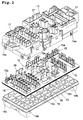
- Fig. 1 is an exploded perspective view showing an upper case, a circuit unit and a lower case of the joint box according to the invention
- Fig. 1 is an exploded perspective view showing an embodiment of the joint box including the circuit board according to the invention.
- the joint box is formed by composing an upper case 11, a circuit unit 12 and a lower case 13. That is to say, the circuit unit 12 is sandwiched between the upper case 11 and the lower case 13, and then the upper case 11 and lower case 13 are coupled with each other by means of locking portions 14a and 14b.
- a given circuit pattern is formed, but for the sake of clarity, the circuit pattern is not shown in the drawing.
- the block bodies 16 are clamped into frame portions 17 formed in the upper case 11 such that connecting portions such as flat blade ends 15a, reception ends 15b and pin ends 15c situate within the frame portions 17.
- connecting portions such as flat blade ends 15a, reception ends 15b and pin ends 15c situate within the frame portions 17.
- connectors accommodating fuse elements, switch elements and another connecting terminals may be connected to these connecting portions.
- connection terminals 15 are extended downward from block bodies 16 provided on a lower surface of the circuit unit 12 and similar electrical elements and connectors may be coupled with the lower surface of the lower case 13.
- electronic circuit units may be provided in the joint box.
- terminals may be provided to extend outwardly and adjacent joint boxes each including electronic circuit units may be coupled with each other by means of the terminals.
- the circuit unit 12 comprises a stack of five circuit boards 19 and each of the circuit boards 19 includes a resin plate 20 having a thickness of about 1.5 mm and a foil circuit 21 having a given circuit pattern as illustrated in Figs. 2 and 3, the foil circuit 21 being placed on the resin plate 20.
- the resin plate 20 may be formed by injection molding of synthetic resin.
- the foil circuit 21 may be formed by a copper foil having thickness of 120 ⁇ m.
- the five circuit boards 19 have respective foil circuits 21 having different circuit patterns.
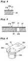
- the resin plate 20 have a plurality of anchor pins 20a extending upward at given positions on a surface thereof. These anchor pins 20a are inserted into pin receiving holes 21a formed in the foil circuit 21 as depicted in Fig. 4.
- the foil circuit 21 is fixed to the resin plate 20 by heating and pushing downward top portions of the anchor pins 20a.
- one or more foil circuits 21 may include two or more than two metal foils as shown in Fig. 5.
- two metal foils 21 are fixed to the resin plate 20 by means of anchor pin 20a' having a larger length.
- the stacked metal foils 21 are coupled with one another by inserting a welding electrode through a welding hole portion 20b.
- a plurality of circular terminal receiving holes 20c are formed in the resin plate 20 as illustrated in Figs. 2 and 3 such that in the stack of the circuit boards 19, these terminal receiving holes 20c are aligned with one another.
- each metal foil circuit 21 has formed therein a hole having an identical diameter as that of the terminal receiving hole 20c and a reception terminal 22 is provided in this hole. It should be noted that there are prepared various reception terminals 22 having different sizes depending upon a desired current capacity and, accordingly, the corresponding terminal receiving holes 20c having different diameters are prepared.
- the reception terminal 22 is made from a brass plate with a thickness of 0.2 mm and is formed by a forming press. As illustrated in Fig. 6, the reception terminal 22 comprises a tubular connecting portion 22a having a relatively small length, a flange portion 22b and a tab portion 22c extending from the flange portion 22b. Furthermore, a tapered guide portion 22d for guiding an insertion terminal is formed between the tubular connecting portion 22a and the flange portion 22b.
- Fig. 7 is a cross sectional view showing a major portion of the circuit unit 12 in which five circuit boards 19 are stacked one another and the reception terminals 22 are provided at given positions.
- An inner diameter of the terminal receiving holes 20c of the circuit boards 19 is substantially identical with an outer diameter of the tubular connecting portion 22a of the reception terminal 22.
- Peripheries of upper end portions of the terminal receiving holes 20c are raised outwardly to form circular ring portions 20d, and step portions 20e are formed in the circular ring portions 20d.
- a lower half of the terminal receiving hole 20c has a larger diameter such that a lower end of the tubular connecting portion 22a can be extended outwardly.
- the terminal receiving holes 20c into which the reception terminals 22 are not inserted have an inner diameter substantially identical with that of the reception terminal 22, but according to the invention, all the terminal receiving holes 20c may be formed to have an identical diameter.
- the tubular connecting portions 22a of the reception terminal 22 is situated within the terminal receiving hole 20c and a lower portion of the tubular connecting portion 22a is calked to the terminal receiving hole 20c by widening a lower end of the connecting portion 22a.
- a primary object of the of widening the lower end of the tubular connecting portion 22a is to fix the reception terminal 22 to the circuit board 19, but it also serves as a tapered guide portion 22e upon inserting a insertion terminal 15 into the reception terminal 22 from the bottom side.
- the tab portions 22c are fused onto the foil circuits 21 of the circuit boards 19. To this end, welding holes 20f are formed in given resin plates 20 at given positions corresponding to the tab portions 22c.
- the circular ring portions 20g provided in the uppermost circuit board 19 of the circuit unit 12 has a same level as the circular ring portions 20d provided at the terminal receiving holes 20c into which the reception terminals 22 are inserted, and therefore the block bodies 16 can be placed on the uppermost circuit board stably.
- the thermally fused top portions of the anchor pins 20a, circular ring portions 20d and reception terminals 22 are clamped into depressions formed in a lower surface of an upper resin plate 20 such that the circuit boards 19 in the stack are brought into intimate contact with one another and could not be deviated horizontally, i.e. laterally.
- the reception terminals 22 secured to a lower level circuit board 19 are clamped into depressions 20j shown in Fig. 3.
- each resin plate 20 there are formed through holes 201 at four corners, said through holes 201 serving as positioning holes for stacking the circuit boards 19.
- each of the circuit boards 19 further includes rectangular holes 20m for securing large current connection terminals 26 shown in Fig. 1 when only the reception terminals 22 could not share a required large current.
- the rectangular holes 20m are formed only in the uppermost circuit board 19 in the circuit unit 12.
- All the circuit boards 19 are not always stacked in such a fashion that the foil circuits 21 face upwardly.
- upper three circuit boards 19 are stacked with the foil circuits 21 facing upward and lower two circuit boards 19 are stacked such that the foil circuits 21 face downward.
- the third and fourth circuit boards 19 are partially clamped with each other not to deviate laterally.
- Fig. 8 is a perspective view depicting the insertion terminal 15 to be inserted into the reception terminal 22.
- a lower end of the insertion terminal 15 is formed as a substantially pin-shaped inserting end 15d which is inserted into the tubular connecting portion 22a of the reception terminal 22.
- the lower inserting end 15d extends via a middle portion 15e to an upper end which protrudes from the upper case 11.
- the upper portion is shaped in the form of a flat blade end 15a.
- the upper portion 15a of the insertion terminal 15 may be formed as the reception ends 15b or pin ends 15c shown in Fig. 1.
- the pin-shaped inserting end 15d of the insertion terminal 15 is formed by folding a thin metal plate into a rod-shaped body having a rectangular cross section without vacant space. Therefore, although use is made of a metal plate having a very small thickness, it is possible to form the inserting end 15d having a side sufficiently wider than a thickness of the metal plate. Therefore, the inserting end 15d could hardly bent or broken. Moreover, the upper flat blade end 15a of the insertion terminal 15 is formed by folding the metal plate such that a thickness of the flat blade end 15a is larger than a thickness of the metal plate by two times.
- plural steps may be formed in the inserting end 15d.
- Middle portions 15e of several insertion terminals 15 are inserted into terminal insertion holes formed in the block bodies 16 made of synthetic resin. As depicted in Fig. 1, all the inserting ends 15d of the insertion terminals 15 are inserted into the circuit boards 19. It should be noted that in order to fix the middle portions 15e of the insertion terminals 15 to the inserting holes, claw portions not shown in the drawings are provided on the middle portions 15e of the insertion terminals 15.
- a single or plural anchor pin 16a are formed to extend from the bottom of the block body 16 and are inserted into the pin receiving holes 21b formed in the foil circuits 21 as well as the pin receiving holes 20k commonly formed in the respective resin plates 20.
- a lower end of the anchor pin 16a projecting out of the lowermost circuit board 19 is melted and pushed against the lowermost circuit board 19. In this manner, the block body 16 can be fixed to the circuit unit 12 and a plurality of circuit boards 19 within the stack can be stably fixed one another.
- Fig. 10 shows another embodiment of the circuit board 19 according to the invention.
- a diameter of terminal receiving holes 20c formed in successive layer circuit boards 19 is gradually reduced, and a diameter of reception terminals 22 provided in successive layer circuit boards 19 is reduced accordingly.
- a diameter of pin-shaped inserting ends of 15d of insertion terminals 15 is gradually reduced as shown in Fig. 11. Therefore, the insertion terminals 15 secured to the block bodies 16 can be inserted into the stack of circuit boards 19.
- Fig. 12 is an explanatory diagram representing successive steps of the method of manufacturing the circuit board 19 according to the invention.
- a copper foil 41 used for the foil circuit 21 as a starting material is wound around a roller 42 in the form of a coil.
- the copper foil 41 is fed intermittently by means of a transporting device 43 such as a clamp. Top this end, pilot holes may be formed in the copper foil 41.
- the copper foil 41 is fed to a hole forming press section and a plurality of pin receiving holes 21a and 21b are formed at a plurality of given positions by means of a hole forming press 44. Then, the copper foil 41 is transported to a section for stacking copper foil onto a resin plate 20.
- the pin receiving holes 21a formed in the copper foil 41 are used to fix the foil circuit 21 to the resin plate 20, and thus the pin receiving holes 21a are formed in a portion of the copper foil 21 which is to be remained on the resin plate 20, said portion of the copper foil constituting the foil circuit 21.
- a number of resin plates 20 are held in a stocker 45 and are fed one by one in synchronism with the transportation of the copper foil 41.
- the resin plate 20 may be formed by the injection molding of a synthetic resin film or by hot pressing of a synthetic resin substrate.
- the resin plate 20 has formed therein anchor pins 20a, hole portions 20b, 20f, terminal receiving holes 20c, circular ring portions 20d, 20g, step portions 20e, electric wire holding recesses 20h, hole portions 20i, depressions 20j, pin receiving holes 20k, through holes 201 and so on.
- the stacking stand 46 moves upward toward the copper foil 41.
- Position of the stacking stand 46 is controlled in a three-dimensional manner by suitably processing an image signal supplied from an image pick-up camera system 47 such that the anchor pins 20a provided on the resin plate 20 are inserted into the pin receiving holes 21a formed in the copper foil 41.
- a heat press 48 situating above the stacking stand 46 is moved downward and top portions of the anchor pins 20a are fused to clamp the copper foil 41 onto the resin plate 20. Since the positioning has been performed, the pin receiving holes 21b formed in the copper foil 41 into which the anchor pins 16a of the block bodies 16 have been inserted are aligned with the pin receiving holes 20k formed in the resin plate 20.
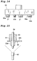
- the punching press 49 includes Thompson blades 49a and the foil circuit 21 can be punched out of the copper foil 41 without injuring the resin plate 20.
- the punching press 49 includes Thompson blades 49a and the foil circuit 21 can be punched out of the copper foil 41 without injuring the resin plate 20.
- the copper foil 41 is fed together with the resin plate 20, and wasted portions of the copper foil 41 which are not used in the foil circuit 21 are pealed off the resin plate 20 and are cut into pieces by a cutter 50. These pieces of copper foil 41 are thrown into a waste box 51.
- the resin plate 20 having the foil circuit 21 secured onto its surface constitutes a circuit board 19 and the thus formed circuit board 19 is fed in a given direction and is stacked in a stocker 52.
- Fig. 13 is an explanatory diagram showing another embodiment of the method of manufacturing the circuit board 19 according to the invention.
- similar portions to those shown in Fig. 12 are denoted by the same reference numerals used in Fig. 12.
- a copper foil 41 serving as a starting material of a foil circuit 21 is wound around a roller 42 in the shape of a coil.
- the copper foil 41 there are formed a number of pin receiving holes 21a, 21b by means of a hole forming press 44 .
- the copper foil 41 is fed into a circuit pattern punching section like as the embodiment illustrated in Fig. 12.
- the copper foil 41 is fed to a punching press 55 and a foil circuit 21 is punched out of the copper foil 41, while a suitable image processing is performed.
- the punching press 55 includes a number of Thompson blades 55a to cut the copper foil 41 into the foil circuit 21 having a given pattern. Between successive Thompson blades 55a, there are provided a plurality of suction pads 55b to suck and hold the punched out foil circuit 21. Then, the foil circuit 21 is fed into a given position by means of a Thompson blade transporting device not shown in the drawings.
- a remaining portion of the copper foil 41 is fed to a cutting blade 56 and is cut into pieces. These pieces of the copper foil 41 are thrown into a waste box 57.
- the resin plate 20 stacked within a stocker 45 are fed one by one onto a stacking stand 46.
- the feeding of the copper foil 41 is synchronized with the punching operation at the punching press 55.
- the foil circuit 21 held by the Thompson blades 55a is fed onto the resin plate 20 transported on the stacking stand 46.
- a position of a Thompson blade transporting device not shown in the drawings is controlled in a three-dimensional manner, while an image processing is performed using an image pick-up camera system 58 such that the anchor pins 20a are inserted into the pin receiving holes 21a formed in the foil circuit 21.
- the foil circuit 21 After inserting the anchor pins 20a into the pin receiving holes 21a of the foil circuit 21 to place the foil circuit 21 on the resin plate 20 at a given position, an air blows from the suction pads 55b against the foil circuit 21 to separate the foil circuit 21 from the Thompson blades 55a and to push the foil circuit 21 onto the resin plate 20. It should be noted that the foil circuit 21 may be pushed onto the resin plate 20 by means of pushing pins provided between successive Thompson blades 55a.
- the Thompson blades 55a are transported by the Thompson blade transporting device into the original position on the punching press 55.
- a heat press 48 is moved downward onto the resin plate 20 having the foil circuit 21 placed thereon and top portions of the anchor pins 20a are fused and then are pushed against the foil circuit 21 to fix the foil circuit 21 onto the resin plate 20.
- Figs. 15-17 are explanatory diagrams showing a process for fixing the reception terminal 22 to the circuit board 19.
- a number of reception terminals 22 are successively fed in an aligned manner by means of a parts feeder, and a reception terminal 22 is held by a robot hand 61 as shown in Fig. 15 and is fed into a given position above the circuit board 19, while an image processing is performed by treating an image signal supplied from an image pick-up camera system 62.
- the robot hand 61 includes a tubular member 63 and a hanging pin 64 which is arranged movably up and down through the tubular member 63. The hanging pin 64 is inserted into a tubular connecting portion 22a of a reception terminal 22 and the reception terminal 22 is held by the hanging pin 64 due to a frictional resistance.
- a mutual position of the robot hand 61 and a circuit board 19 is controlled by the image processing and the reception terminal 22 is inserted into a terminal receiving hole 20c such that a tab portion 22c of the reception terminal 22 is placed on a foil circuit 21 provided on the resin plate 20.
- the hanging pin 64 is moved upward.
- a press pin 65 having a conical tip is moved upward into the terminal receiving hole 20c to push and expand outwardly a lower end of the tubular connecting portion 22a to clamp the reception terminal 22 to the resin plate 20 as depicted in Fig. 16.
- the tab portion 22c is welled to the foil circuit 21 by means of electrodes 66 and 67 as illustrated in Fig. 17. Tips of the electrodes 66 and 67 are formed in the shape of a circular rod having a diameter of about 1 mm.
- the upper electrode 66 is brought into contact with the tab portion 22c and the lower electrode 67 is brought into contact with the lower surface of the foil circuit 21 through the welding hole 20f formed in the resin plate 20.
- the tab portions 22c of a plurality of reception terminals 22 may be welled to the foil circuit 21 successively using a robot hand or may be simultaneously welled to the foil circuit 21 by means of a plurality of welding electrodes.
- FIGs. 18-20 are explanatory diagrams representing a process of securing the rectangular electric wire 23 into the wire holding recess 20h formed in the resin plate 20.
- a rectangular electric wire 71 comprising a rectangular copper wire having a cross section of 0.3mmx3mm and an electrically insulating coating applied on the copper wire is wound on a roller 72 as depicted in Fig. 18.
- the rectangular electric wire 71 is rewound intermittently from the roller 72 and is first passed through correcting rollers 73 to remove undesired twist, while an amount of feeding of the electric wire 71 is measured by a length measuring rollers 74. After the rectangular electric wire 71 has been fed by a given length, the wire 71 is fixed by a chuck 75.
- the insulating coating applied on a given portion of the electric wire 71 is removed by a pealing machine 76.
- the electric wire 71 is fed again such that said portion of the electric wire 71 from which the insulating coating has been pealed off is fed into a cutter 77, and the electric wire 71 is cut at a middle of said portion while fixed by a chuck 78.
- both ends of the electric wire 23 are bent by means of a work pressing machine 79 as shown in Fig. 19.
- the rectangular electric wire 23 is held by a robot hand and is inserted into the electric wire holding recess 20h.
- both ends of the rectangular electric wire 23 from which the insulating coating has been removed are pushed against the rear surface of the foil circuit 21 through wire inserting holes 20i formed in the resin plate 20, while an image signal supplied from an image pick-up camera system 80 is suitably processed.
- the both ends of the rectangular electric wire 23 are welded to the foil circuit 21 by means of welding electrodes 81, 82.
- a plurality of the circuit boards 19 having different circuit patterns as stacked one another and the block bodies 16 are placed on the stack of the circuit boards 19 as shown in Fig. 9 to insert the inserting ends 15d of the insertion terminals 15 fixed to the block bodies 19 are inserted into the terminal receiving holes 20c formed in the circuit boards 19. Then, the inserting ends 15d of these insertion terminals 15 are inserted into the tubular connecting portions 22a of the reception terminals 22 secured to the circuit boards 19.
- the inserting end 15d of the insertion terminal 15 is formed to have a substantially square cross section, corner portions of the inserting end are brought into contact with the tubular connecting portion 22a of the reception terminal 22 in a sufficient manner and a good electrical connection can be attained between the insertion terminal 15 and at least one foil circuit 21 of one or more circuit boards 19.
- the block bodies 16 are mounted on the circuit unit 12 from a lower side.
- the anchor pins 16a extending from the block bodies 16 are passed through the pin receiving holes 20k formed in the stack of circuit boards 19. Then, tip portions of the anchor pins 16a projecting from the pin receiving holes 20k are fused to complete the manufacturing of the circuit unit 12.
- this formed circuit unit 12 is sandwiched between the upper case 11 and the lower case 13, and these cases are locked with each other by means of the locking portions 14a, 14b. Finally the above mentioned various kinds of elements and connectors are connected to the flat blade ends 15a, receiving ends 15b and pin ends 15c to form the joint box.
- Figs. 21-27 show another embodiment of the circuit board according to the invention.
- a respective circuit board 91 comprises a resin plate 92 formed by the injection molding of an electrically insulating synthetic resin and having a maximum thickness of about 1.5 mm, and foil circuits 93 formed by a copper foil having a thickness of 120 ⁇ m.
- the foil circuits 93 are formed to have given circuit patterns and are placed on the resin plate 92.
- depressed portions 94 In a top surface of the resin plate 92, there are formed depressed portions 94 having contour configuration corresponding to respective foil circuits 93 and having a depth identical with a thickness of the foil circuits 93. Therefore, the foil circuits 93 can be easily placed on the resin plate 92 at correct positions.
- the resin plate 92 has formed therein a plurality of anchor pins 92a extending upwardly.
- the anchor pins 92a are inserted into pin receiving holes 93a formed in the foil circuits 93.
- the foil circuits 93 can be fixed to the resin plate 92.
- two or more than two foil circuits 93 may be stacked like as the previous embodiment.
- reception ring 95 is formed as a circular ring, but may be formed as a rectangular or square ring. There are prepared various kinds of reception rings 95 having different sizes corresponding to different current capacities, and therefore the terminal receiving holes 92b have different sizes.
- the reception ring 95 is made of stainless steel and is formed by cutting a pipe having a circular or rectangular or square cross section. It should be noted that the reception ring 95 may include a flange portion 95a as illustrated in Fig. 23.
- the foil circuits 93 situating above the reception rings 95 clamped into the terminal receiving holes 92b, there are formed cross-wire cut portions 93b.
- the cut portion 93b is expanded and the foil circuit 93 is clamped between the reception ring 95 and the inserting end 96d of the connection terminal 96 to establish a good electrical connection between the inserting end 95d and the foil circuit 93.
- the reception ring 95 is not clamped, and in circuit patterns around the terminal receiving holes 92b, openings are formed or removed not to be electrically conductive.
- connection terminal 96 By sharpening the inserting end 96d as depicted in Fig. 21, the connection terminal 96 can be easily inserted. Furthermore, the inserting end 96d of the connection terminal 96 is formed to have a square cross section also as shown in Fig. 21, and therefore the cross-wire cut portion 93b can be easily expanded and a good contact can be attained between the inserting end 96d of the connection terminal 96 and the reception ring 95.
- a cross-wire cut portion 93b is formed in the foil circuit 93 as shown in Fig. 25(a), but according to the invention, a circular hole 93c shown in Fig. 25(b) or a rectangular hole 93d depicted in Fig. 25(c) may be formed in the foil circuit 93.
- Fig. 26 is a cross sectional view showing a major portion of a circuit unit 97 including a stack of five circuit boards 91. At four corners of respective circuit boards 91 there are formed protrusions and depressions by means of which the circuit boards 91 can be stacked stably.
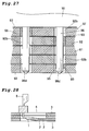
- a plurality of circuit boards 91 each having different circuit patterns are stacked one another and block bodies 16 are placed on the uppermost circuit board 91 as shown in Fig. 27 and inserting ends 96d of connection terminals 96 fixed to the block bodies 16 are inserted into terminal receiving holes 92b formed in the circuit boards 91. Then, the inserting ends 96d of the connection terminals 96 are brought into contact with the reception rings 95 provided in the circuit boards 91 and are electrically connected to the foil circuits 93 to form the three-dimensional circuit unit 97 using the stack of the circuit boards 91.
Landscapes
- Engineering & Computer Science (AREA)
- Microelectronics & Electronic Packaging (AREA)
- Manufacturing & Machinery (AREA)
- Architecture (AREA)
- Civil Engineering (AREA)
- Structural Engineering (AREA)
- Coupling Device And Connection With Printed Circuit (AREA)
- Combinations Of Printed Boards (AREA)
- Connection Or Junction Boxes (AREA)
- Manufacturing Of Printed Wiring (AREA)
- Structure Of Printed Boards (AREA)
- Printing Elements For Providing Electric Connections Between Printed Circuits (AREA)
- Production Of Multi-Layered Print Wiring Board (AREA)
Abstract
A circuit board with a simple structure is manufactured. A circuit board 19 has thereon a foil circuit 21 provided on a synthetic resin plate 20 formed by injection molding, made of a copper foil, and having a pattern different for circuit board 19. Anchor pins 20a projecting upward are provided on the resin plate 20 and passed through pinholes made in the foil circuit 21. The foil circuit 21 are positioned and secured to the resin plate 20. In a required portion of the resin plate 20, a terminal insertion hole 20c is provided, and receiving terminal 22 is secured to the required portion of the terminal insertion hole 20c and connected to the foil circuit 21.
Description
- The present invention relates to a circuit board for use in various electronic devices and joint boxes for connecting, dividing and joining various kinds of electric wires, a method of manufacturing such a circuit board, and also relates to a joint box including such circuit boards.
- There have been known various types of joint boxes. For instant, in Document 1 (
Japanese Patent Publication Kokai Hei 10-243526 insulating sheets 2 to form aflat cable layer 3 as illustrated in Fig. 28. - A plurality of
flat cable layers 3 are stacked one another and a plurality ofcommon holes 4 are formed in such a manner that a conductive foil 1 of a givenflat cable layer 3 is exposed within respectivecommon holes 4. Then, an exposed portion of the relevant conductive foil 1 is fused to a lower end of aconnection terminal 5 provided on the uppermostflat cable layer 3. - Document 1:
Japanese Patent Application Kokai Hei 10-243526 - In the above-mentioned known joint box, the
flat cable layers 3 could not be formed easily and a manufacturing cost is liable to increase. Furthermore, the operation for connecting the conductive foil 1 to theconnection terminal 5 via thehole 4 is cumbersome and the electrical connection between the conductive foil 1 and theconnection terminal 5 is liable to unstable. - The present invention has for its object to provide a circuit board which can remove the above mentioned problems of the known circuit board and can be used for various electrical devices. It is another object of the invention to provide a method of manufacturing a circuit board in easy and less expensive manner. It is still another object of the invention to provide a joint box including such circuit boards.
- According to one aspect of the invention, a circuit board comprises a resin plate formed by a three-dimensional mold of an electrically insulating synthetic resin; and a circuit pattern formed by a metal foil and placed on said resin plate.
- According to another aspect of the present invention, a circuit board comprises a resin plate formed by a three-dimensional mold of an electrically insulating synthetic resin; a circuit pattern formed by at least one foil circuit punched out of a metal foil into a given pattern and placed on said resin plate; and a plurality of reception terminals provided in a plurality of terminal receiving holes formed in said resin plate such that said reception terminals are connected to said circuit pattern.
- According to another aspect of the invention, a circuit board comprises a resin plate formed by a three-dimensional mold of an electrically insulating synthetic resin; a circuit pattern formed by at least one foil circuit punched out of a metal foil into a given pattern and placed on said resin plate; and a plurality of tubular reception terminals clamped in a plurality of terminal receiving holes formed in said resin plate; whereby said metal foil of the circuit pattern has formed therein a plurality of cut portions at positions corresponding to said terminal receiving holes such that a plurality of connection terminals can be inserted into said reception terminals through said cut portions.
- The present invention also relates to a method of manufacturing a circuit board and provides a method of manufacturing a circuit board comprising a resin plate formed by a three-dimensional mold of an electrically insulating synthetic resin and a circuit pattern placed on said resin plate, comprising:
- punching said circuit pattern out of a metal foil into a given pattern by means of Thompson blades;
- holding said circuit pattern between said Thompson blades;
- transporting said circuit pattern onto said resin plate; and
- fixing said circuit pattern to said resin plate.
- Thee present invention also relates to a joint box
including circuit boards, and provides a joint box comprising:
a stack of circuit boards each of which includes a resin plate formed by a three-dimensional mold of an electrically insulating synthetic resin and a circuit pattern formed by at least one foil circuit punched out of a metal foil into a given pattern and placed on said resin plate;
a plurality of terminal receiving holes commonly formed in the stacked circuit boards;
a plurality of tubular metal reception terminals each of which includes a tab portion and is provided in a terminal receiving hole formed in a given layer circuit board of said stack, said tab portion being connected to a circuit pattern of the relevant circuit board; and
a plurality of insertion terminals including pin-shaped inserting ends inserted into said terminal receiving holes such that the insertion terminals are connected to said reception terminals to establish electrically connection between said circuit patterns of the circuit boards. - According to another aspect of the invention, a joint box comprises:
- a stack of circuit boards each of which includes a resin plate formed by a three-dimensional mold of an electrically insulating synthetic resin and a circuit pattern formed by at least one foil circuit punched out of a metal foil into a given pattern and placed on said resin plate;
- a plurality of terminal receiving holes commonly formed in resin plates of the stacked circuit boards;
- a plurality of cut portions formed in said circuit patterns;
- a plurality of tubular metal reception terminals provided in said terminal receiving holes formed in given layer circuit boards; and
- a plurality of insertion terminals having pin-shaped inserting ends inserted into said terminal receiving holes through said cut portions such that the insertion terminals are connected to said reception terminals to establish electrically connection between said circuit patterns of the circuit boards.
- According to a method of manufacturing a circuit board in the invention, since a circuit pattern formed by a metal foil and placed on said resin plate, simple formation and manufacturing of a circuit board is feasible.
- According to a joint box in the invention, since a stack of circuit boards comprising a circuit pattern formed by a foil circuit punched out of a metal foil, a thinner joint box can be manufactured even in a complex circuit.
- Fig. 1 is an exploded perspective view showing an upper case, a circuit unit and a lower case of the joint box according to the invention;
- Fig. 2 is a plan view illustrating the circuit board according to the invention;
- Fig. 3 is a bottom view of the circuit board;
- Fig. 4 is a cross sectional view depicting a part of the circuit board;
- Fig. 5 is a cross sectional view showing a part of the circuit board comprising two metal foils stacked one on the other;
- Fig. 6 is a perspective view illustrating a reception terminal;
- Fig. 7 is a cross sectional view depicting a major portion of the circuit board having reception terminals fixed thereto;
- Fig. 8 is a perspective view showing an insertion terminal;
- Fig. 9 is a cross sectional view illustrating the circuit board and block body;
- Fig. 10 is across sectional view depicting a major portion of another embodiment of the stacked circuit boards having reception terminals fixed thereto;
- Fig. 11 is a perspective view showing another embodiment of the insertion terminal;
- Fig. 12 is an explanatory diagram illustrating successive processes of the method of manufacturing the circuit board according to the invention;
- Fig. 13 is an explanatory diagram illustrating successive processes of another embodiment of the method of manufacturing the circuit board according to the invention;
- Fig. 14 is a cross sectional view showing a step of holding a foil circuit with a Thompson blade;
- Fig. 15 is an explanatory diagram illustrating a step of holding a reception terminal with a robot hand;
- Fig. 16 is an explanatory diagram of a step of fixing a reception terminal to a circuit board;
- Fig. 17 is an explanatory diagram of a step of fusing a reception terminal to a foil circuit;
- Fig. 18 is an explanatory diagram of a step in which a rectangular electric wire is formed;
- Fig. 19 is an explanatory diagram of a step of folding a rectangular electric wire;
- Fig. 20 is an explanatory diagram of a step of fusing a rectangular electric wire to a foil circuit;
- Fig. 21 is a perspective view showing a process of assembling another embodiment of the circuit board according to the invention;
- Fig. 22 is an expanded perspective view illustrating a reception ring;
- Fig. 23 is a perspective view depicting another embodiment of the reception ring;
- Fig. 24 is a cross sectional view showing a condition in which an insertion end is inserted into the reception ring via a foil circuit;
- Figs. 25(a), 25(b) and 25(c) are plan views depicting several embodiments of the cut portion;
- Fig. 26 is a cross sectional view illustrating a major part of the circuit unit formed by a stack of circuit boards;
- Fig. 27 is a cross sectional view showing a condition in which an insertion end is inserted into the stacked circuit boards; and
- Fig. 28 is a cross sectional view depicting a portion of a known circuit board.
-
- 12, 97
- Circuit unit
- 15
- Insertion terminal
- 16
- Block body
- 19, 91
- Circuit board
- 20, 92
- Resin plate
- 20c, 92b
- Terminal receiving hole
- 21, 93
- Metal foil circuit
- 22
- Reception terminal
- 23
- Rectangular electric wire
- 41
- Copper foil
- 49, 55
- Punching press
- 49a, 55a
- Thompson blade
- 55b
- Suction pad
- 71
- ctric wire
- 95
- Roller
- 96
- Connecting terminal
- A present invention will be explained in detail according to embodiments shown in Fig.1 to Fig. 27.
- Fig. 1 is an exploded perspective view showing an embodiment of the joint box including the circuit board according to the invention. The joint box is formed by composing an
upper case 11, acircuit unit 12 and alower case 13. That is to say, thecircuit unit 12 is sandwiched between theupper case 11 and thelower case 13, and then theupper case 11 andlower case 13 are coupled with each other by means of lockingportions - On an upper surface of the
circuit unit 12, a given circuit pattern is formed, but for the sake of clarity, the circuit pattern is not shown in the drawing. On the upper surface of thecircuit unit 12, there are arranged a plurality ofblock bodies 16 made of a synthetic resin and a plurality ofinsertion terminals 15 are secured to eachblock bodies 16. Theblock bodies 16 are clamped intoframe portions 17 formed in theupper case 11 such that connecting portions such as flat blade ends 15a, reception ends 15b and pin ends 15c situate within theframe portions 17. It should be noted that connectors accommodating fuse elements, switch elements and another connecting terminals may be connected to these connecting portions. - In the
lower case 13 there are also formedframe portions 18, and connecting ends of theconnection terminals 15 are extended downward fromblock bodies 16 provided on a lower surface of thecircuit unit 12 and similar electrical elements and connectors may be coupled with the lower surface of thelower case 13. - It should be noted that electronic circuit units may be provided in the joint box. Furthermore, terminals may be provided to extend outwardly and adjacent joint boxes each including electronic circuit units may be coupled with each other by means of the terminals.
- The
circuit unit 12 comprises a stack of fivecircuit boards 19 and each of thecircuit boards 19 includes aresin plate 20 having a thickness of about 1.5 mm and afoil circuit 21 having a given circuit pattern as illustrated in Figs. 2 and 3, thefoil circuit 21 being placed on theresin plate 20. Theresin plate 20 may be formed by injection molding of synthetic resin. Thefoil circuit 21 may be formed by a copper foil having thickness of 120 µm. The fivecircuit boards 19 haverespective foil circuits 21 having different circuit patterns. - The
resin plate 20 have a plurality of anchor pins 20a extending upward at given positions on a surface thereof. These anchor pins 20a are inserted intopin receiving holes 21a formed in thefoil circuit 21 as depicted in Fig. 4. Thefoil circuit 21 is fixed to theresin plate 20 by heating and pushing downward top portions of the anchor pins 20a. - Depending upon a current capacity, one or
more foil circuits 21 may include two or more than two metal foils as shown in Fig. 5. In the embodiment shown in Fig. 5, two metal foils 21 are fixed to theresin plate 20 by means ofanchor pin 20a' having a larger length. The stacked metal foils 21 are coupled with one another by inserting a welding electrode through awelding hole portion 20b. - A plurality of circular
terminal receiving holes 20c are formed in theresin plate 20 as illustrated in Figs. 2 and 3 such that in the stack of thecircuit boards 19, theseterminal receiving holes 20c are aligned with one another. In acircuit board 19 of a given layer within the stack of circuit boards, eachmetal foil circuit 21 has formed therein a hole having an identical diameter as that of theterminal receiving hole 20c and areception terminal 22 is provided in this hole. It should be noted that there are preparedvarious reception terminals 22 having different sizes depending upon a desired current capacity and, accordingly, the correspondingterminal receiving holes 20c having different diameters are prepared. - The
reception terminal 22 is made from a brass plate with a thickness of 0.2 mm and is formed by a forming press. As illustrated in Fig. 6, thereception terminal 22 comprises atubular connecting portion 22a having a relatively small length, aflange portion 22b and atab portion 22c extending from theflange portion 22b. Furthermore, atapered guide portion 22d for guiding an insertion terminal is formed between the tubular connectingportion 22a and theflange portion 22b. - Fig. 7 is a cross sectional view showing a major portion of the
circuit unit 12 in which fivecircuit boards 19 are stacked one another and thereception terminals 22 are provided at given positions. An inner diameter of theterminal receiving holes 20c of thecircuit boards 19 is substantially identical with an outer diameter of thetubular connecting portion 22a of thereception terminal 22. Peripheries of upper end portions of theterminal receiving holes 20c are raised outwardly to formcircular ring portions 20d, andstep portions 20e are formed in thecircular ring portions 20d. A lower half of theterminal receiving hole 20c has a larger diameter such that a lower end of thetubular connecting portion 22a can be extended outwardly. - It should be noted that in the present embodiment, the
terminal receiving holes 20c into which thereception terminals 22 are not inserted have an inner diameter substantially identical with that of thereception terminal 22, but according to the invention, all theterminal receiving holes 20c may be formed to have an identical diameter. - The tubular connecting
portions 22a of thereception terminal 22 is situated within theterminal receiving hole 20c and a lower portion of thetubular connecting portion 22a is calked to theterminal receiving hole 20c by widening a lower end of the connectingportion 22a. A primary object of the of widening the lower end of thetubular connecting portion 22a is to fix thereception terminal 22 to thecircuit board 19, but it also serves as atapered guide portion 22e upon inserting ainsertion terminal 15 into thereception terminal 22 from the bottom side. Thetab portions 22c are fused onto thefoil circuits 21 of thecircuit boards 19. To this end,welding holes 20f are formed in givenresin plates 20 at given positions corresponding to thetab portions 22c. - Around upper ends of terminal receiving
holes 20c into which noreception terminals 22 of thecircuit boards 19 are not inserted, there are formedcircular ring proportions 20g such that theinsertion terminals 15 are not contacted with thefoil circuits 21 although thefoil circuits 21 are existent around theseterminal receiving holes 20c. Thecircular ring portions 20g provided in theuppermost circuit board 19 of thecircuit unit 12 has a same level as thecircular ring portions 20d provided at theterminal receiving holes 20c into which thereception terminals 22 are inserted, and therefore theblock bodies 16 can be placed on the uppermost circuit board stably. - As shown in Figs. 2 and 3, in the lower surfaces of the
resin plates 20, there are formed electricwire receiving recesses 20h into which rectangularelectric wires 23 having electrically insulating coatings applied thereon are inserted. Both ends of each rectangularelectric wire 23 are bent upwardly through electricwire inserting holes 20i and are fused to lower surfaces offoil circuits 21. Then, the rectangularelectric wires 23 serve as a jumper for electrically connecting circuit patterns of thefoil circuits 21 which could not be connected to each other on the surface of theresin plate 20. It should be noted that there are prepared various kinds of the rectangularelectric wires 23 having different cross sectional areas depending on the current capacity. - The thermally fused top portions of the anchor pins 20a,
circular ring portions 20d andreception terminals 22 are clamped into depressions formed in a lower surface of anupper resin plate 20 such that thecircuit boards 19 in the stack are brought into intimate contact with one another and could not be deviated horizontally, i.e. laterally. For instance, thereception terminals 22 secured to a lowerlevel circuit board 19 are clamped intodepressions 20j shown in Fig. 3. In eachresin plate 20 there are formed throughholes 201 at four corners, said throughholes 201 serving as positioning holes for stacking thecircuit boards 19. - As depicted in Figs. 2 and 3, each of the
circuit boards 19 further includesrectangular holes 20m for securing largecurrent connection terminals 26 shown in Fig. 1 when only thereception terminals 22 could not share a required large current. Therectangular holes 20m are formed only in theuppermost circuit board 19 in thecircuit unit 12. - All the
circuit boards 19 are not always stacked in such a fashion that thefoil circuits 21 face upwardly. In Fig. 7, upper threecircuit boards 19 are stacked with thefoil circuits 21 facing upward and lower twocircuit boards 19 are stacked such that thefoil circuits 21 face downward. Although not shown in the drawings, the third andfourth circuit boards 19 are partially clamped with each other not to deviate laterally. - Fig. 8 is a perspective view depicting the
insertion terminal 15 to be inserted into thereception terminal 22. A lower end of theinsertion terminal 15 is formed as a substantially pin-shaped insertingend 15d which is inserted into thetubular connecting portion 22a of thereception terminal 22. The lower insertingend 15d extends via amiddle portion 15e to an upper end which protrudes from theupper case 11. In order to connect the upper portion of theinsertion terminal 15 to other connecting terminal, the upper portion is shaped in the form of aflat blade end 15a. It should be noted that theupper portion 15a of theinsertion terminal 15 may be formed as the reception ends 15b or pin ends 15c shown in Fig. 1. - The pin-shaped inserting
end 15d of theinsertion terminal 15 is formed by folding a thin metal plate into a rod-shaped body having a rectangular cross section without vacant space. Therefore, although use is made of a metal plate having a very small thickness, it is possible to form the insertingend 15d having a side sufficiently wider than a thickness of the metal plate. Therefore, the insertingend 15d could hardly bent or broken. Moreover, the upperflat blade end 15a of theinsertion terminal 15 is formed by folding the metal plate such that a thickness of theflat blade end 15a is larger than a thickness of the metal plate by two times. - In order to attain a feeling of click upon inserting the
insertion terminal 15 into thereception terminal 22 as well as a good electrical connection, plural steps may be formed in the insertingend 15d. There are prepared various kinds of theinsertion holes 15d having the inserting ends of different sizes corresponding to sizes of thereception terminals 22. -
Middle portions 15e ofseveral insertion terminals 15 are inserted into terminal insertion holes formed in theblock bodies 16 made of synthetic resin. As depicted in Fig. 1, all the inserting ends 15d of theinsertion terminals 15 are inserted into thecircuit boards 19. It should be noted that in order to fix themiddle portions 15e of theinsertion terminals 15 to the inserting holes, claw portions not shown in the drawings are provided on themiddle portions 15e of theinsertion terminals 15. - As shown in Fig. 9, a single or
plural anchor pin 16a are formed to extend from the bottom of theblock body 16 and are inserted into thepin receiving holes 21b formed in thefoil circuits 21 as well as thepin receiving holes 20k commonly formed in therespective resin plates 20. A lower end of theanchor pin 16a projecting out of thelowermost circuit board 19 is melted and pushed against thelowermost circuit board 19. In this manner, theblock body 16 can be fixed to thecircuit unit 12 and a plurality ofcircuit boards 19 within the stack can be stably fixed one another. - Fig. 10 shows another embodiment of the
circuit board 19 according to the invention. In the stack ofcircuit boards 19, a diameter of terminal receivingholes 20c formed in successivelayer circuit boards 19 is gradually reduced, and a diameter ofreception terminals 22 provided in successivelayer circuit boards 19 is reduced accordingly. At the same time, a diameter of pin-shaped inserting ends of 15d ofinsertion terminals 15 is gradually reduced as shown in Fig. 11. Therefore, theinsertion terminals 15 secured to theblock bodies 16 can be inserted into the stack ofcircuit boards 19. - Fig. 12 is an explanatory diagram representing successive steps of the method of manufacturing the
circuit board 19 according to the invention. Acopper foil 41 used for thefoil circuit 21 as a starting material is wound around aroller 42 in the form of a coil. Thecopper foil 41 is fed intermittently by means of a transportingdevice 43 such as a clamp. Top this end, pilot holes may be formed in thecopper foil 41. At first thecopper foil 41 is fed to a hole forming press section and a plurality ofpin receiving holes hole forming press 44. Then, thecopper foil 41 is transported to a section for stacking copper foil onto aresin plate 20. It should be noted that thepin receiving holes 21a formed in thecopper foil 41 are used to fix thefoil circuit 21 to theresin plate 20, and thus thepin receiving holes 21a are formed in a portion of thecopper foil 21 which is to be remained on theresin plate 20, said portion of the copper foil constituting thefoil circuit 21. - A number of
resin plates 20 are held in astocker 45 and are fed one by one in synchronism with the transportation of thecopper foil 41. Theresin plate 20 may be formed by the injection molding of a synthetic resin film or by hot pressing of a synthetic resin substrate. Theresin plate 20 has formed therein anchor pins 20a,hole portions terminal receiving holes 20c,circular ring portions step portions 20e, electricwire holding recesses 20h,hole portions 20i, depressions 20j, pin receivingholes 20k, throughholes 201 and so on. - After a
resin plate 20 has been transported from thestocker 45 onto a stackingstand 46, the stackingstand 46 moves upward toward thecopper foil 41. Position of the stackingstand 46 is controlled in a three-dimensional manner by suitably processing an image signal supplied from an image pick-upcamera system 47 such that the anchor pins 20a provided on theresin plate 20 are inserted into thepin receiving holes 21a formed in thecopper foil 41. - When a large current capacity is required, two sheets of the
copper foil 41 are stacked on theresin plate 20 to reduce an electric resistance for a current passing through thefoil circuit 21. In this case, the above explained process is repeated twice, and then the stacked copper sheets are mutually fused using the fusingholes 20b formed in theresin plate 20 as shown in Fig. 5. - After inserting the anchor pins 20a into the
pin receiving holes 21a to stack thecopper foil 41 on theresin plate 20, aheat press 48 situating above the stackingstand 46 is moved downward and top portions of the anchor pins 20a are fused to clamp thecopper foil 41 onto theresin plate 20. Since the positioning has been performed, thepin receiving holes 21b formed in thecopper foil 41 into which the anchor pins 16a of theblock bodies 16 have been inserted are aligned with thepin receiving holes 20k formed in theresin plate 20. - Next, the assembly of the
resin plate 20 andcopper foil 41 is fed into a punchingpress 49 and thecopper foil 41 is punched into a given pattern to form thefoil circuit 21. The punchingpress 49 includesThompson blades 49a and thefoil circuit 21 can be punched out of thecopper foil 41 without injuring theresin plate 20. Upon punching thefoil circuit 21, when a portion of thecopper foil 41 which will be connected to one ormore reception terminals 22 in thefinal circuit board 19, one or more terminal receiving holes having a diameter identical with an inner diameter of thereception circuit 22 are formed. When a portion of thecopper foil 41 which will be not connected to anyreception terminal 22, one or more holes having a diameter identical with an outer diameter of a peripheral portion of thecircuit ring portion 20g are formed. - Furthermore, the
copper foil 41 is fed together with theresin plate 20, and wasted portions of thecopper foil 41 which are not used in thefoil circuit 21 are pealed off theresin plate 20 and are cut into pieces by acutter 50. These pieces ofcopper foil 41 are thrown into awaste box 51. Theresin plate 20 having thefoil circuit 21 secured onto its surface constitutes acircuit board 19 and the thus formedcircuit board 19 is fed in a given direction and is stacked in astocker 52. - Fig. 13 is an explanatory diagram showing another embodiment of the method of manufacturing the
circuit board 19 according to the invention. In the present embodiment, similar portions to those shown in Fig. 12 are denoted by the same reference numerals used in Fig. 12. Acopper foil 41 serving as a starting material of afoil circuit 21 is wound around aroller 42 in the shape of a coil. In thecopper foil 41 there are formed a number ofpin receiving holes hole forming press 44 . Thecopper foil 41 is fed into a circuit pattern punching section like as the embodiment illustrated in Fig. 12. - Next, the
copper foil 41 is fed to a punchingpress 55 and afoil circuit 21 is punched out of thecopper foil 41, while a suitable image processing is performed. As illustrated in Fig. 14, the punchingpress 55 includes a number ofThompson blades 55a to cut thecopper foil 41 into thefoil circuit 21 having a given pattern. Betweensuccessive Thompson blades 55a, there are provided a plurality ofsuction pads 55b to suck and hold the punched outfoil circuit 21. Then, thefoil circuit 21 is fed into a given position by means of a Thompson blade transporting device not shown in the drawings. - A remaining portion of the
copper foil 41 is fed to acutting blade 56 and is cut into pieces. These pieces of thecopper foil 41 are thrown into awaste box 57. - The
resin plate 20 stacked within astocker 45 are fed one by one onto a stackingstand 46. The feeding of thecopper foil 41 is synchronized with the punching operation at the punchingpress 55. Then, thefoil circuit 21 held by theThompson blades 55a is fed onto theresin plate 20 transported on the stackingstand 46. During this operation, a position of a Thompson blade transporting device not shown in the drawings is controlled in a three-dimensional manner, while an image processing is performed using an image pick-upcamera system 58 such that the anchor pins 20a are inserted into thepin receiving holes 21a formed in thefoil circuit 21. - After inserting the anchor pins 20a into the
pin receiving holes 21a of thefoil circuit 21 to place thefoil circuit 21 on theresin plate 20 at a given position, an air blows from thesuction pads 55b against thefoil circuit 21 to separate thefoil circuit 21 from theThompson blades 55a and to push thefoil circuit 21 onto theresin plate 20. It should be noted that thefoil circuit 21 may be pushed onto theresin plate 20 by means of pushing pins provided betweensuccessive Thompson blades 55a. - After that, the
Thompson blades 55a are transported by the Thompson blade transporting device into the original position on the punchingpress 55. Aheat press 48 is moved downward onto theresin plate 20 having thefoil circuit 21 placed thereon and top portions of the anchor pins 20a are fused and then are pushed against thefoil circuit 21 to fix thefoil circuit 21 onto theresin plate 20. - Figs. 15-17 are explanatory diagrams showing a process for fixing the
reception terminal 22 to thecircuit board 19. A number ofreception terminals 22 are successively fed in an aligned manner by means of a parts feeder, and areception terminal 22 is held by arobot hand 61 as shown in Fig. 15 and is fed into a given position above thecircuit board 19, while an image processing is performed by treating an image signal supplied from an image pick-upcamera system 62. Therobot hand 61 includes atubular member 63 and a hangingpin 64 which is arranged movably up and down through thetubular member 63. The hangingpin 64 is inserted into atubular connecting portion 22a of areception terminal 22 and thereception terminal 22 is held by the hangingpin 64 due to a frictional resistance. A mutual position of therobot hand 61 and acircuit board 19 is controlled by the image processing and thereception terminal 22 is inserted into aterminal receiving hole 20c such that atab portion 22c of thereception terminal 22 is placed on afoil circuit 21 provided on theresin plate 20. - While the
reception terminal 22 is urged against astep portion 20e of theresin plate 20 by thetubular member 63, the hangingpin 64 is moved upward. Next, apress pin 65 having a conical tip is moved upward into theterminal receiving hole 20c to push and expand outwardly a lower end of thetubular connecting portion 22a to clamp thereception terminal 22 to theresin plate 20 as depicted in Fig. 16. - Then, the
tab portion 22c is welled to thefoil circuit 21 by means ofelectrodes electrodes upper electrode 66 is brought into contact with thetab portion 22c and thelower electrode 67 is brought into contact with the lower surface of thefoil circuit 21 through thewelding hole 20f formed in theresin plate 20. It should be noted that thetab portions 22c of a plurality ofreception terminals 22 may be welled to thefoil circuit 21 successively using a robot hand or may be simultaneously welled to thefoil circuit 21 by means of a plurality of welding electrodes. - Figs. 18-20 are explanatory diagrams representing a process of securing the rectangular
electric wire 23 into thewire holding recess 20h formed in theresin plate 20. A rectangularelectric wire 71 comprising a rectangular copper wire having a cross section of 0.3mmx3mm and an electrically insulating coating applied on the copper wire is wound on aroller 72 as depicted in Fig. 18. The rectangularelectric wire 71 is rewound intermittently from theroller 72 and is first passed through correctingrollers 73 to remove undesired twist, while an amount of feeding of theelectric wire 71 is measured by alength measuring rollers 74. After the rectangularelectric wire 71 has been fed by a given length, thewire 71 is fixed by achuck 75. While theelectric wire 71 is fixed, the insulating coating applied on a given portion of theelectric wire 71 is removed by a pealingmachine 76. When theelectric wire 71 is fed again such that said portion of theelectric wire 71 from which the insulating coating has been pealed off is fed into acutter 77, and theelectric wire 71 is cut at a middle of said portion while fixed by achuck 78. - In this manner, it is possible to obtain a rectangular
electric wire 23 having a given length; while the insulating coating applied on both ends of theelectric wire 23 have been removed. Then, both ends of theelectric wire 23 are bent by means of awork pressing machine 79 as shown in Fig. 19. After turning theresin plate 20 up side down, the rectangularelectric wire 23 is held by a robot hand and is inserted into the electricwire holding recess 20h. Then, as shown in Fig. 20, both ends of the rectangularelectric wire 23 from which the insulating coating has been removed are pushed against the rear surface of thefoil circuit 21 throughwire inserting holes 20i formed in theresin plate 20, while an image signal supplied from an image pick-upcamera system 80 is suitably processed. Then, the both ends of the rectangularelectric wire 23 are welded to thefoil circuit 21 by means ofwelding electrodes - A plurality of the
circuit boards 19 having different circuit patterns as stacked one another and theblock bodies 16 are placed on the stack of thecircuit boards 19 as shown in Fig. 9 to insert the inserting ends 15d of theinsertion terminals 15 fixed to theblock bodies 19 are inserted into theterminal receiving holes 20c formed in thecircuit boards 19. Then, the inserting ends 15d of theseinsertion terminals 15 are inserted into the tubular connectingportions 22a of thereception terminals 22 secured to thecircuit boards 19. - Since the inserting
end 15d of theinsertion terminal 15 is formed to have a substantially square cross section, corner portions of the inserting end are brought into contact with thetubular connecting portion 22a of thereception terminal 22 in a sufficient manner and a good electrical connection can be attained between theinsertion terminal 15 and at least onefoil circuit 21 of one ormore circuit boards 19. As a case may be, theblock bodies 16 are mounted on thecircuit unit 12 from a lower side. - When the inserting ends 15d are inserted, the anchor pins 16a extending from the
block bodies 16 are passed through thepin receiving holes 20k formed in the stack ofcircuit boards 19. Then, tip portions of the anchor pins 16a projecting from thepin receiving holes 20k are fused to complete the manufacturing of thecircuit unit 12. - Next, the this formed
circuit unit 12 is sandwiched between theupper case 11 and thelower case 13, and these cases are locked with each other by means of the lockingportions - Figs. 21-27 show another embodiment of the circuit board according to the invention. As illustrated in Fig. 21, a
respective circuit board 91 comprises aresin plate 92 formed by the injection molding of an electrically insulating synthetic resin and having a maximum thickness of about 1.5 mm, and foilcircuits 93 formed by a copper foil having a thickness of 120 µm. Thefoil circuits 93 are formed to have given circuit patterns and are placed on theresin plate 92. In a top surface of theresin plate 92, there are formeddepressed portions 94 having contour configuration corresponding torespective foil circuits 93 and having a depth identical with a thickness of thefoil circuits 93. Therefore, thefoil circuits 93 can be easily placed on theresin plate 92 at correct positions. - The
resin plate 92 has formed therein a plurality of anchor pins 92a extending upwardly. When thefoil circuits 93 are placed on theresin plate 92, the anchor pins 92a are inserted intopin receiving holes 93a formed in thefoil circuits 93. By fusing tips of the anchor pins 92a, thefoil circuits 93 can be fixed to theresin plate 92. When a large current capacity is required, two or more than twofoil circuits 93 may be stacked like as the previous embodiment. - In
resin plates 92 stacked one another, there are commonly formed circularterminal receiving holes 92b and circular reception rings 95 shown in Fig. 22 are inserted intoterminal receiving holes 92b formed in givencircuit board 91. Thereception ring 95 is formed as a circular ring, but may be formed as a rectangular or square ring. There are prepared various kinds of reception rings 95 having different sizes corresponding to different current capacities, and therefore theterminal receiving holes 92b have different sizes. Thereception ring 95 is made of stainless steel and is formed by cutting a pipe having a circular or rectangular or square cross section. It should be noted that thereception ring 95 may include aflange portion 95a as illustrated in Fig. 23. - In the
foil circuits 93 situating above the reception rings 95 clamped into theterminal receiving holes 92b, there are formedcross-wire cut portions 93b. When an insertingend 96d of aconnection terminal 96 is inserted into thecross-wire cut portion 93b as illustrated in Fig. 24, thecut portion 93b is expanded and thefoil circuit 93 is clamped between thereception ring 95 and the insertingend 96d of theconnection terminal 96 to establish a good electrical connection between the inserting end 95d and thefoil circuit 93. At the inserting end 95d which is not required to be electrically conductive, thereception ring 95 is not clamped, and in circuit patterns around theterminal receiving holes 92b, openings are formed or removed not to be electrically conductive. - By sharpening the inserting
end 96d as depicted in Fig. 21, theconnection terminal 96 can be easily inserted. Furthermore, the insertingend 96d of theconnection terminal 96 is formed to have a square cross section also as shown in Fig. 21, and therefore thecross-wire cut portion 93b can be easily expanded and a good contact can be attained between the insertingend 96d of theconnection terminal 96 and thereception ring 95. - In the present embodiment, a
cross-wire cut portion 93b is formed in thefoil circuit 93 as shown in Fig. 25(a), but according to the invention, acircular hole 93c shown in Fig. 25(b) or arectangular hole 93d depicted in Fig. 25(c) may be formed in thefoil circuit 93. - Fig. 26 is a cross sectional view showing a major portion of a
circuit unit 97 including a stack of fivecircuit boards 91. At four corners ofrespective circuit boards 91 there are formed protrusions and depressions by means of which thecircuit boards 91 can be stacked stably. - A plurality of
circuit boards 91 each having different circuit patterns are stacked one another and blockbodies 16 are placed on theuppermost circuit board 91 as shown in Fig. 27 and insertingends 96d ofconnection terminals 96 fixed to theblock bodies 16 are inserted intoterminal receiving holes 92b formed in thecircuit boards 91. Then, the inserting ends 96d of theconnection terminals 96 are brought into contact with the reception rings 95 provided in thecircuit boards 91 and are electrically connected to thefoil circuits 93 to form the three-dimensional circuit unit 97 using the stack of thecircuit boards 91.
Claims (22)
- A circuit board comprising a resin plate formed by a three-dimensional mold of an electrically insulating synthetic resin; and a circuit pattern formed by a metal foil and placed on said resin plate.
- The circuit board according to claim 1, wherein said circuit pattern is formed by at least one foil circuit punched out of a metal foil into a given pattern, said foil circuit being fixed onto said resin plate.
- The circuit board according to claim 2, wherein said circuit pattern includes a plurality of pin receiving holes into which anchor pins extending from the resin plate are inserted to fix said circuit pattern onto the resin plate.
- The circuit board according claim 1, wherein said resin plate has at least one recess formed in a rear surface thereof, and both ends of a jumper wire held in said recess are connected to said circuit pattern.
- The circuit board according to claim 2, wherein said circuit pattern is formed by a plurality of metal foils which are stacked on said resin plate.
- A circuit board comprising a resin plate formed by a three-dimensional mold of an electrically insulating synthetic resin; a circuit pattern formed by at least one foil circuit punched out of a metal foil into a given pattern and placed on said resin plate; and a plurality of reception terminals provided in a plurality of terminal receiving holes formed in said resin plate such that said reception terminals are connected to said circuit pattern.
- The circuit board according to claim 6, wherein said reception terminal includes a tab portion which is welded to said circuit pattern.
- A circuit board comprising a resin plate formed by a three-dimensional mold of an electrically insulating synthetic resin; a circuit pattern formed by at least one foil circuit punched out of a metal foil into a given pattern and placed on said resin plate; and a plurality of tubular reception terminals clamped in a plurality of terminal receiving holes formed in said resin plate; whereby said metal foil of the circuit pattern has formed therein a plurality of cut portions at positions corresponding to said terminal receiving holes such that a plurality of connection terminals can be inserted into said reception terminals through said cut portions.
- The circuit board according to claim 8, wherein inserting ends of said connection terminals are inserted into said reception terminals through said cut portions formed in said metal foil to electrically connect said metal foil to said insertion terminals.
- The circuit board according to claim 8 or 9, wherein said cut portions are formed as a cross-wire cut.
- A method of manufacturing a circuit board comprising a resin plate formed by a three-dimensional mold of an electrically insulating synthetic resin and a circuit pattern placed on said resin plate, comprising:punching said circuit pattern out of a metal foil into a given pattern by means of Thompson blades;holding said circuit pattern between said Thompson blades;transporting said circuit pattern onto said resin plate; andfixing said circuit pattern to said resin plate.
- The method according to claim 11, wherein said circuit pattern is held between the Thompson blades by air suction nozzles provided between successive Thompson blades.
- The method according to claim 11, wherein said circuit pattern is placed onto said resin plate by air blowing portions provided between successive Thompson blades.
- The method according to claim 11, wherein said circuit pattern is placed onto said resin plate by a plurality of pin-shaped pushing rods provided between successive Thompson blades.
- A joint box comprising:a stack of circuit boards each of which includes a resin plate formed by a three-dimensional mold of an electrically insulating synthetic resin and a circuit pattern formed by at least one foil circuit punched out of a metal foil into a given pattern and placed on said resin plate;a plurality of terminal receiving holes commonly formed in the stacked circuit boards;a plurality of tubular metal reception terminals each of which includes a tab portion and is provided in a terminal receiving hole formed in a given layer circuit board of said stack, said tab portion being connected to a circuit pattern of the relevant circuit board; anda plurality of insertion terminals including pin-shaped inserting ends inserted into said terminal receiving holes such that the insertion terminals are connected to said reception terminals to establish electrically connection between said circuit patterns of the circuit boards.
- The joint box according to claim 15, wherein said tab portions of the reception terminals are connected to said circuit patterns by welding.
- A joint box comprising:a stack of circuit boards each of which includes a resin plate formed by a three-dimensional mold of an electrically insulating synthetic resin and a circuit pattern formed by at least one foil circuit punched out of a metal foil into a given pattern and placed on said resin plate;a plurality of terminal receiving holes commonly formed in resin plates of the stacked circuit boards;a plurality of cut portions formed in said circuit patterns;a plurality of tubular metal reception terminals provided in said terminal receiving holes formed in given layer circuit boards; anda plurality of insertion terminals having pin-shaped inserting ends inserted into said terminal receiving holes through said cut portions such that the insertion terminals are connected to said reception terminals to establish electrically connection between said circuit patterns of the circuit boards.
- The joint box according to claim 15 or 17, wherein said circuit boards include protrusions and depressions and are stacked by clamping corresponding protrusions and depressions one another.
- The joint box according to claim 15 or 17, wherein one end of said insertion terminal constitutes said pin-shaped inserting end and the other end constitutes a connecting terminal having such a shape that another connecting terminal is clamped into said connecting terminal.
- The joint box according to claim 19, wherein said inserting end has a rectangular cross section.
- The joint box according to claim 19, wherein said insertion terminals are secured to at least one block body made of electrically insulating synthetic resin by fixing middle portions of the insertion terminals between the inserting ends and connecting ends to fitting holes formed in said block body, and said block body is placed on one surface of the stack of circuit boards to insert simultaneously said inserting ends of the insertion terminals into said terminal receiving holes formed in the circuit boards.
- The joint box according to claim 21, wherein a plurality of anchor pins are provided on a bottom surface of said block body and are inserted into pin receiving holes formed in the stack of circuit boards, and the circuit boards in the stack are fixed to one another by fusing end portions of the anchor pings extending from the other surface of the stack of circuit boards.
Applications Claiming Priority (4)
| Application Number | Priority Date | Filing Date | Title |
|---|---|---|---|
| JP2004105997 | 2004-03-31 | ||
| JP2004239707 | 2004-08-19 | ||
| JP2004381266 | 2004-12-28 | ||
| PCT/JP2005/005811 WO2005096683A1 (en) | 2004-03-31 | 2005-03-29 | Circuit board, its manufacturing method, and joint box using circuit board |
Publications (2)
| Publication Number | Publication Date |
|---|---|
| EP1737282A1 true EP1737282A1 (en) | 2006-12-27 |
| EP1737282A4 EP1737282A4 (en) | 2010-05-05 |
Family
ID=35064168
Family Applications (1)
| Application Number | Title | Priority Date | Filing Date |
|---|---|---|---|
| EP05727833A Withdrawn EP1737282A4 (en) | 2004-03-31 | 2005-03-29 | Circuit board, its manufacturing method, and joint box using circuit board |
Country Status (6)
| Country | Link |
|---|---|
| US (3) | US7943859B2 (en) |
| EP (1) | EP1737282A4 (en) |
| JP (4) | JPWO2005096683A1 (en) |
| KR (3) | KR101208823B1 (en) |
| CN (2) | CN100594757C (en) |
| WO (1) | WO2005096683A1 (en) |
Cited By (3)
| Publication number | Priority date | Publication date | Assignee | Title |
|---|---|---|---|---|
| EP2007178A3 (en) * | 2007-06-21 | 2013-12-11 | Robert Bosch Gmbh | Electronic device with at least one electric connected element and method for producing a connected element |
| GB2566943A (en) * | 2017-09-25 | 2019-04-03 | Ge Aviat Systems Ltd | Surface mount connector and method of forming a printed circuit board |
| EP2716143B1 (en) * | 2011-05-24 | 2019-09-04 | JUMATECH GmbH | Printed circuit board having a molded part and method for the production thereof |
Families Citing this family (29)
| Publication number | Priority date | Publication date | Assignee | Title |
|---|---|---|---|---|
| CN100594757C (en) * | 2004-03-31 | 2010-03-17 | 三菱电线工业株式会社 | Circuit board, method for manufacturing the same, and junction box using the same |
| DE102008008278A1 (en) * | 2008-02-07 | 2009-08-13 | Dr. Johannes Heidenhain Gmbh | Angle measuring device |
| JP2010027957A (en) * | 2008-07-23 | 2010-02-04 | Mitsubishi Cable Ind Ltd | Circuit structure, joint box, and method of manufacturing circuit structure |
| JP5255365B2 (en) * | 2008-08-09 | 2013-08-07 | 古河電気工業株式会社 | Relay terminal member, circuit structure including the same, and electronic unit |
| JP5497389B2 (en) * | 2009-09-17 | 2014-05-21 | 三菱マテリアル株式会社 | Electrical junction box |
| JP5758584B2 (en) | 2010-03-18 | 2015-08-05 | 本田技研工業株式会社 | Junction box |
| CN101958521A (en) * | 2010-09-19 | 2011-01-26 | 淮南润成科技有限公司 | Distributing box for mine substantial security circuit |
| JP5610285B2 (en) * | 2010-09-29 | 2014-10-22 | 本田技研工業株式会社 | Wiring structure and joint box including the same |
| US8491315B1 (en) * | 2011-11-29 | 2013-07-23 | Plastronics Socket Partners, Ltd. | Micro via adapter socket |
| US9536798B2 (en) * | 2012-02-22 | 2017-01-03 | Cyntec Co., Ltd. | Package structure and the method to fabricate thereof |
| JP5952039B2 (en) * | 2012-03-15 | 2016-07-13 | 住友精密工業株式会社 | Discharge cell and ozone gas generator |
| DE102012009651A1 (en) * | 2012-05-14 | 2013-11-14 | Robert Bosch Gmbh | Connection unit for drive device, has terminal pins that are provided at injection molding structure for electrically connecting electrical terminal of electrical loads to an electrical energy source |
| DE202012010075U1 (en) * | 2012-10-22 | 2012-11-13 | Truma Gerätetechnik GmbH & Co. KG | Central unit for shunting drive |
| JP2015049053A (en) * | 2013-08-29 | 2015-03-16 | アルプス・グリーンデバイス株式会社 | Current detector |
| CN104953011B (en) * | 2015-06-26 | 2016-05-11 | 深圳市峻泽科技有限公司 | A substrate with a metal layer and its manufacturing method |
| US10104784B2 (en) | 2015-11-06 | 2018-10-16 | Nxp B.V. | Method for making an electronic product with flexible substrate |
| US9994407B2 (en) | 2015-11-06 | 2018-06-12 | Nxp B.V. | System and method for processing a flexible substrate |
| US20170223816A1 (en) * | 2016-02-01 | 2017-08-03 | Ibiden Co., Ltd. | Flexible printed wiring board, electronic device having flexible printed wiring board, and method for manufacturing electronic device having flexible printed wiring board |
| WO2018114688A1 (en) * | 2016-12-19 | 2018-06-28 | Abb Schweiz Ag | Laminated busbar for plug-in modules |
| JP2019029535A (en) * | 2017-07-31 | 2019-02-21 | イビデン株式会社 | Flexible printed wiring board, electronic device having flexible printed wiring board, method for manufacturing electronic device having flexible printed wiring board |
| JP6666320B2 (en) | 2017-11-21 | 2020-03-13 | ファナック株式会社 | Mounting structure of resin molded board and capacitor |
| JP7094619B2 (en) * | 2018-01-29 | 2022-07-04 | 矢崎総業株式会社 | Route structure and method |
| CN108901134B (en) * | 2018-07-12 | 2023-07-25 | 深圳智慧者机器人科技有限公司 | Copper plate assembling device |
| JP7289706B2 (en) * | 2019-04-08 | 2023-06-12 | 矢崎エナジーシステム株式会社 | joint box |
| US11374366B2 (en) | 2020-06-19 | 2022-06-28 | Lear Corporation | System and method for providing an electrical ground connection for a circuit assembly |
| JP2022026387A (en) * | 2020-07-31 | 2022-02-10 | 日本電産エレシス株式会社 | Motor control device and electric power steering device |
| US11646514B2 (en) | 2020-08-10 | 2023-05-09 | Lear Corporation | Surface mount technology terminal header and method for providing an electrical connection to a printed circuit board |
| US11706867B2 (en) | 2021-01-27 | 2023-07-18 | Lear Corporation | System and method for providing an electrical ground connection for a circuit assembly |
| CN113161948B (en) * | 2021-02-09 | 2022-12-09 | 国网福建省电力有限公司明溪县供电公司 | Extrusion type self-sealing type junction box |
Family Cites Families (67)
| Publication number | Priority date | Publication date | Assignee | Title |
|---|---|---|---|---|
| US3674914A (en) * | 1968-02-09 | 1972-07-04 | Photocircuits Corp | Wire scribed circuit boards and method of manufacture |
| US3688248A (en) * | 1968-08-13 | 1972-08-29 | Henry John Modrey | Roller metal pin for use as electric connector or fastener |
| FR2217906B3 (en) * | 1973-02-15 | 1976-02-13 | Radiall Fr | |
| JPS5575294A (en) * | 1978-12-02 | 1980-06-06 | Sumitomo Electric Industries | Method of connecting back and front surfaces of bothhside printed circuit board |
| US4333233A (en) * | 1979-02-19 | 1982-06-08 | Guardall Limited | Machines and method applicable to the manufacture of electrical and like devices |
| US4435741A (en) * | 1980-09-03 | 1984-03-06 | Canon Kabushiki Kaisha | Electrical circuit elements combination |
| JPS58106971U (en) * | 1982-01-14 | 1983-07-21 | 棚沢 日佐司 | printed wiring board |
| US4487463A (en) * | 1983-02-22 | 1984-12-11 | Gulf & Western Manufacturing Company | Multiple contact header assembly |
| JPS59230741A (en) * | 1983-06-15 | 1984-12-25 | 株式会社日立製作所 | shape memory composite material |
| JPS618960U (en) * | 1984-06-22 | 1986-01-20 | 日本航空電子工業株式会社 | Elastic pin for press-fitting |
| US4641426A (en) * | 1985-06-21 | 1987-02-10 | Associated Enterprises, Inc. | Surface mount compatible connector system with mechanical integrity |
| DE3581940D1 (en) * | 1985-12-11 | 1991-04-04 | Burndy Electra Nv | CONTACT PEN. |
| JPS63127222U (en) * | 1987-02-09 | 1988-08-19 | ||
| JPS63229897A (en) * | 1987-03-19 | 1988-09-26 | 古河電気工業株式会社 | Manufacture of rigid type multilayer printed circuit board |
| US4937932A (en) * | 1987-04-10 | 1990-07-03 | Ishii Hyoki Co., Ltd. | Membrane panel switch |
| US4769907A (en) * | 1987-07-27 | 1988-09-13 | Northern Telecom Limited | Method of making a circuit board pin |
| US4948375A (en) * | 1987-08-25 | 1990-08-14 | Howard Lawrence | Adaptor assembly for circuit boards |
| US4867691A (en) * | 1987-10-29 | 1989-09-19 | E. I. Du Pont De Nemours And Company | Connector having expansible barrel with a layer of reflowable solder material thereon |
| JP2582142B2 (en) * | 1988-04-27 | 1997-02-19 | 日本電信電話株式会社 | Matrix switch board, matrix switch board connection pin, and method of manufacturing matrix board |
| US4950170A (en) * | 1988-06-23 | 1990-08-21 | Ltv Aerospace & Defense Company | Minimal space printed circuit board and electrical connector system |
| US4996629A (en) * | 1988-11-14 | 1991-02-26 | International Business Machines Corporation | Circuit board with self-supporting connection between sides |
| JPH02239684A (en) * | 1989-03-14 | 1990-09-21 | Yazaki Corp | Formation of circuit pattern on resin compact |
| JPH0744041Y2 (en) * | 1990-04-30 | 1995-10-09 | 古河電気工業株式会社 | Printed wiring board for large current |
| JP2573531B2 (en) * | 1991-05-22 | 1997-01-22 | 三菱電機株式会社 | Large current wiring board |
| JP2827621B2 (en) * | 1991-10-23 | 1998-11-25 | 三菱電機株式会社 | High current substrate and method of manufacturing the same |
| JPH05167207A (en) | 1991-12-13 | 1993-07-02 | Okuma Mach Works Ltd | Printed board for power circuit wiring and manufacture thereof |
| US5373626A (en) * | 1993-01-06 | 1994-12-20 | Elco Corporation | Removable pin carrier |
| JP2849888B2 (en) * | 1993-02-02 | 1999-01-27 | 矢崎総業株式会社 | Wiring junction box |
| JP3163592B2 (en) * | 1993-04-01 | 2001-05-08 | 矢崎総業株式会社 | Composite circuit board |
| US5456608A (en) * | 1993-08-25 | 1995-10-10 | Conx Corporation | Cross-connect system |
| US6031349A (en) * | 1993-08-25 | 2000-02-29 | Con-X Corporation | Cross-connect method and apparatus |
| JPH07122825A (en) * | 1993-10-22 | 1995-05-12 | Sharp Corp | Three-dimensional molded circuit board and manufacturing method thereof |
| JP3170124B2 (en) * | 1993-12-07 | 2001-05-28 | 矢崎総業株式会社 | Circuit body multi-layer connection structure and circuit body multi-layer connection method |
| WO1995015919A1 (en) * | 1993-12-08 | 1995-06-15 | Massachusetts Institute Of Technology | Casting tooling |
| US5836582A (en) * | 1994-04-04 | 1998-11-17 | Canon Kabushiki Kaisha | Sheet feeding device with air injectors for separating sheets |
| EP0708046A1 (en) * | 1994-10-21 | 1996-04-24 | Maschinenfabrik Gietz Ag | Register and feeding device |
| JPH08153425A (en) | 1994-11-28 | 1996-06-11 | Furukawa Electric Co Ltd:The | Method for manufacturing flat circuit body |
| US5788513A (en) * | 1995-01-11 | 1998-08-04 | Enplas Corporation | IC socket |
| JPH08222825A (en) * | 1995-02-13 | 1996-08-30 | Nec Corp | Connecting structure of printed board |
| JP2953335B2 (en) | 1995-02-14 | 1999-09-27 | 住友電装株式会社 | Branch junction box |
| JPH08322127A (en) * | 1995-05-23 | 1996-12-03 | Sumitomo Wiring Syst Ltd | Laminated structure of bus bar and insulating plate contained in electric connection case |
| JPH09153516A (en) | 1995-11-30 | 1997-06-10 | Sumitomo Bakelite Co Ltd | Semiconductor device and IC chip inspection method |
| JPH09163516A (en) * | 1995-12-06 | 1997-06-20 | Yazaki Corp | Wiring board and manufacturing method thereof |
| US5914534A (en) * | 1996-05-03 | 1999-06-22 | Ford Motor Company | Three-dimensional multi-layer molded electronic device and method for manufacturing same |
| JPH10243526A (en) | 1997-02-21 | 1998-09-11 | Ryosei Denso Kk | Joint box |
| DE19707709C1 (en) | 1997-02-26 | 1998-04-16 | Siemens Ag | Relay modules circuit board e.g. for automobile |
| DE19709551A1 (en) * | 1997-03-07 | 1998-09-10 | Wuerth Elektronik Gmbh & Co Kg | Electrical printed circuit board |
| JP3201516B2 (en) * | 1997-07-18 | 2001-08-20 | ユーエイチティー株式会社 | Perforator |
| JP2001127242A (en) * | 1999-10-22 | 2001-05-11 | Seiko Epson Corp | Semiconductor chip, multi-chip package, semiconductor device, electronic device, and manufacturing method thereof |
| US6483041B1 (en) * | 1999-11-12 | 2002-11-19 | Emc Corporation | Micro soldered connection |
| JP2001145241A (en) | 1999-11-15 | 2001-05-25 | Sumitomo Wiring Syst Ltd | Wiring board assembly |
| FR2806249B1 (en) * | 2000-03-13 | 2002-05-10 | Axo Scintex Cie Equip Automobi | MOUNTING OF CUT-OUT CIRCUITS ON LAMP SUPPORTS |
| JP2001264276A (en) * | 2000-03-21 | 2001-09-26 | Polyplastics Co | Sensor having a circuit formed by metal foil transfer |
| JP2001307795A (en) * | 2000-04-18 | 2001-11-02 | Yazaki Corp | Wiring unit and electrical junction box |
| JP2001343906A (en) * | 2000-05-31 | 2001-12-14 | Internatl Business Mach Corp <Ibm> | Display device, liquid crystal display device, method of production and connection for liquid crystal display device |
| JP2001359222A (en) * | 2000-06-13 | 2001-12-26 | Yazaki Corp | Electrical junction box |
| JP2002034126A (en) | 2000-07-19 | 2002-01-31 | Yazaki Corp | Wiring unit |
| JP2002374049A (en) * | 2001-06-13 | 2002-12-26 | Densei Lambda Kk | Mounting structure for power-supply device |
| JP2003017163A (en) * | 2001-06-27 | 2003-01-17 | Gunma Denki Kk | Multi-pin connector for mounting on sub-board and mounting method of parts on printed circuit board |
| JP3884931B2 (en) * | 2001-08-31 | 2007-02-21 | アルプス電気株式会社 | Electronic device FPC connection structure |
| JP2003142178A (en) * | 2001-11-07 | 2003-05-16 | Matsushita Electric Ind Co Ltd | Printed wiring board |
| JP2003249755A (en) * | 2002-02-22 | 2003-09-05 | Kyocera Corp | Method for manufacturing ceramic multilayer wiring board, and ceramic multilayer wiring board |
| JP2004030936A (en) * | 2002-06-21 | 2004-01-29 | Mitsubishi Cable Ind Ltd | Manufacturing method of flat wiring body and conductive foil punching device |
| JP3976627B2 (en) * | 2002-06-25 | 2007-09-19 | 矢崎総業株式会社 | Manufacturing method of electrical junction box |
| JP4141213B2 (en) * | 2002-09-17 | 2008-08-27 | アルプス電気株式会社 | Electrical component and its mounting structure |
| US7099155B2 (en) * | 2003-02-14 | 2006-08-29 | Autonetworks Technologies, Ltd. | Distribution unit and electric connection box including the same |
| CN100594757C (en) * | 2004-03-31 | 2010-03-17 | 三菱电线工业株式会社 | Circuit board, method for manufacturing the same, and junction box using the same |
-
2005
- 2005-03-29 CN CN200580009958A patent/CN100594757C/en not_active Expired - Fee Related
- 2005-03-29 EP EP05727833A patent/EP1737282A4/en not_active Withdrawn
- 2005-03-29 KR KR1020117026550A patent/KR101208823B1/en not_active Expired - Fee Related
- 2005-03-29 KR KR1020117026551A patent/KR101208751B1/en not_active Expired - Fee Related
- 2005-03-29 JP JP2006511657A patent/JPWO2005096683A1/en active Pending
- 2005-03-29 KR KR1020067019950A patent/KR101183336B1/en not_active Expired - Fee Related
- 2005-03-29 WO PCT/JP2005/005811 patent/WO2005096683A1/en not_active Ceased
- 2005-03-29 US US10/593,796 patent/US7943859B2/en not_active Expired - Fee Related
- 2005-03-29 CN CN2009101404406A patent/CN101568227B/en not_active Expired - Fee Related
-
2008
- 2008-03-21 JP JP2008073718A patent/JP4823262B2/en not_active Expired - Fee Related
- 2008-03-21 JP JP2008073717A patent/JP4719759B2/en not_active Expired - Fee Related
-
2009
- 2009-04-14 JP JP2009097640A patent/JP4938046B2/en not_active Expired - Fee Related
-
2011
- 2011-01-13 US US13/006,222 patent/US8362366B2/en not_active Expired - Fee Related
- 2011-01-13 US US13/006,122 patent/US20110120756A1/en not_active Abandoned
Cited By (5)
| Publication number | Priority date | Publication date | Assignee | Title |
|---|---|---|---|---|
| EP2007178A3 (en) * | 2007-06-21 | 2013-12-11 | Robert Bosch Gmbh | Electronic device with at least one electric connected element and method for producing a connected element |
| EP2716143B1 (en) * | 2011-05-24 | 2019-09-04 | JUMATECH GmbH | Printed circuit board having a molded part and method for the production thereof |
| US10736214B2 (en) | 2011-05-24 | 2020-08-04 | Jumatech Gmbh | Printed circuit board having a molded part and method for the production thereof |
| GB2566943A (en) * | 2017-09-25 | 2019-04-03 | Ge Aviat Systems Ltd | Surface mount connector and method of forming a printed circuit board |
| GB2566943B (en) * | 2017-09-25 | 2020-09-02 | Ge Aviat Systems Ltd | Surface mount connector and method of forming a printed circuit board |
Also Published As
| Publication number | Publication date |
|---|---|
| CN1939101A (en) | 2007-03-28 |
| KR20070034460A (en) | 2007-03-28 |
| JP4719759B2 (en) | 2011-07-06 |
| KR101183336B1 (en) | 2012-09-14 |
| JPWO2005096683A1 (en) | 2008-02-21 |
| US20110116248A1 (en) | 2011-05-19 |
| CN101568227B (en) | 2011-09-28 |
| JP2008160156A (en) | 2008-07-10 |
| CN100594757C (en) | 2010-03-17 |
| WO2005096683A1 (en) | 2005-10-13 |
| KR20120003481A (en) | 2012-01-10 |
| KR20110129490A (en) | 2011-12-01 |
| KR101208751B1 (en) | 2012-12-05 |
| US8362366B2 (en) | 2013-01-29 |
| JP2009164632A (en) | 2009-07-23 |
| JP4938046B2 (en) | 2012-05-23 |
| JP4823262B2 (en) | 2011-11-24 |
| CN101568227A (en) | 2009-10-28 |
| KR101208823B1 (en) | 2012-12-06 |
| US7943859B2 (en) | 2011-05-17 |
| US20070218257A1 (en) | 2007-09-20 |
| JP2008220165A (en) | 2008-09-18 |
| US20110120756A1 (en) | 2011-05-26 |
| EP1737282A4 (en) | 2010-05-05 |
Similar Documents
| Publication | Publication Date | Title |
|---|---|---|
| US8362366B2 (en) | Circuit board, its manufacturing method, and joint box using circuit board | |
| US3427715A (en) | Printed circuit fabrication | |
| US5434749A (en) | Hybrid printed circuit board | |
| US4316320A (en) | Method of manufacturing electronic circuit apparatus | |
| US4121044A (en) | Flexible through-contacted printed circuits | |
| TW452946B (en) | Tape carrier and the manufacturing method thereof, tape carrier manufacturing device and manufacturing method for semiconductor device | |
| EP0893945B1 (en) | Printed board and manufacturing method therefor | |
| US4187606A (en) | Flexible electrical jumper and method of making same | |
| US4049334A (en) | Wire preparation and termination means and method | |
| JP2008146944A (en) | Planar wiring body connection portion processing method and planar wiring body and terminal connection portion | |
| JPH0634446B2 (en) | Circuit board soldering method | |
| US6241549B1 (en) | Pressure-contact terminal and electric connection box containing pressure-contact terminals | |
| JP4939634B2 (en) | Circuit board connection terminals | |
| JP4578843B2 (en) | Circuit board connection terminals | |
| JP3375571B2 (en) | Electrical connector and method of soldering cable to this connector | |
| JPH0673868U (en) | Cable connection structure for electronic components | |
| JP2011114159A (en) | Printed board laminate and connection terminal coupler | |
| JP2991324B2 (en) | Connection between circuit conductors and method of connecting circuit conductors | |
| JPH08222332A (en) | Multi-pin contact apparatus of card connector and manufacture thereof | |
| JPH07201433A (en) | Flexible flat conductor cable connection method | |
| JPH0355007B2 (en) | ||
| JPS6199285A (en) | Tape connector and connection method | |
| JP2000350336A (en) | Solderless terminal |
Legal Events
| Date | Code | Title | Description |
|---|---|---|---|
| PUAI | Public reference made under article 153(3) epc to a published international application that has entered the european phase |
Free format text: ORIGINAL CODE: 0009012 |
|
| 17P | Request for examination filed |
Effective date: 20060929 |
|
| AK | Designated contracting states |
Kind code of ref document: A1 Designated state(s): DE FR GB |
|
| DAX | Request for extension of the european patent (deleted) | ||
| RBV | Designated contracting states (corrected) |
Designated state(s): DE FR GB |
|
| A4 | Supplementary search report drawn up and despatched |
Effective date: 20100406 |
|
| 17Q | First examination report despatched |
Effective date: 20110706 |
|
| RAP1 | Party data changed (applicant data changed or rights of an application transferred) |
Owner name: FURUKAWA AUTOMOTIVE SYSTEMS INC. |
|
| STAA | Information on the status of an ep patent application or granted ep patent |
Free format text: STATUS: THE APPLICATION HAS BEEN WITHDRAWN |
|
| 18W | Application withdrawn |
Effective date: 20160525 |