EP1734568A2 - Verfahren zur Herstellung eines isolierten Transistors mit einem verspannten Kanal - Google Patents
Verfahren zur Herstellung eines isolierten Transistors mit einem verspannten Kanal Download PDFInfo
- Publication number
- EP1734568A2 EP1734568A2 EP06115549A EP06115549A EP1734568A2 EP 1734568 A2 EP1734568 A2 EP 1734568A2 EP 06115549 A EP06115549 A EP 06115549A EP 06115549 A EP06115549 A EP 06115549A EP 1734568 A2 EP1734568 A2 EP 1734568A2
- Authority
- EP
- European Patent Office
- Prior art keywords
- layer
- zones
- drain
- source
- channel
- Prior art date
- Legal status (The legal status is an assumption and is not a legal conclusion. Google has not performed a legal analysis and makes no representation as to the accuracy of the status listed.)
- Granted
Links
Images



Classifications
-
- H—ELECTRICITY
- H10—SEMICONDUCTOR DEVICES; ELECTRIC SOLID-STATE DEVICES NOT OTHERWISE PROVIDED FOR
- H10D—INORGANIC ELECTRIC SEMICONDUCTOR DEVICES
- H10D30/00—Field-effect transistors [FET]
- H10D30/60—Insulated-gate field-effect transistors [IGFET]
- H10D30/791—Arrangements for exerting mechanical stress on the crystal lattice of the channel regions
-
- H—ELECTRICITY
- H10—SEMICONDUCTOR DEVICES; ELECTRIC SOLID-STATE DEVICES NOT OTHERWISE PROVIDED FOR
- H10D—INORGANIC ELECTRIC SEMICONDUCTOR DEVICES
- H10D30/00—Field-effect transistors [FET]
- H10D30/60—Insulated-gate field-effect transistors [IGFET]
- H10D30/67—Thin-film transistors [TFT]
- H10D30/6704—Thin-film transistors [TFT] having supplementary regions or layers in the thin films or in the insulated bulk substrates for controlling properties of the device
- H10D30/6713—Thin-film transistors [TFT] having supplementary regions or layers in the thin films or in the insulated bulk substrates for controlling properties of the device characterised by the properties of the source or drain regions, e.g. compositions or sectional shapes
-
- H—ELECTRICITY
- H10—SEMICONDUCTOR DEVICES; ELECTRIC SOLID-STATE DEVICES NOT OTHERWISE PROVIDED FOR
- H10D—INORGANIC ELECTRIC SEMICONDUCTOR DEVICES
- H10D62/00—Semiconductor bodies, or regions thereof, of devices having potential barriers
- H10D62/01—Manufacture or treatment
- H10D62/021—Forming source or drain recesses by etching e.g. recessing by etching and then refilling
-
- H—ELECTRICITY
- H10—SEMICONDUCTOR DEVICES; ELECTRIC SOLID-STATE DEVICES NOT OTHERWISE PROVIDED FOR
- H10D—INORGANIC ELECTRIC SEMICONDUCTOR DEVICES
- H10D62/00—Semiconductor bodies, or regions thereof, of devices having potential barriers
- H10D62/10—Shapes, relative sizes or dispositions of the regions of the semiconductor bodies; Shapes of the semiconductor bodies
- H10D62/17—Semiconductor regions connected to electrodes not carrying current to be rectified, amplified or switched, e.g. channel regions
- H10D62/213—Channel regions of field-effect devices
- H10D62/221—Channel regions of field-effect devices of FETs
- H10D62/235—Channel regions of field-effect devices of FETs of IGFETs
-
- H—ELECTRICITY
- H10—SEMICONDUCTOR DEVICES; ELECTRIC SOLID-STATE DEVICES NOT OTHERWISE PROVIDED FOR
- H10P—GENERIC PROCESSES OR APPARATUS FOR THE MANUFACTURE OR TREATMENT OF DEVICES COVERED BY CLASS H10
- H10P90/00—Preparation of wafers not covered by a single main group of this subclass, e.g. wafer reinforcement
- H10P90/19—Preparing inhomogeneous wafers
- H10P90/1904—Preparing vertically inhomogeneous wafers
- H10P90/1906—Preparing SOI wafers
-
- H—ELECTRICITY
- H10—SEMICONDUCTOR DEVICES; ELECTRIC SOLID-STATE DEVICES NOT OTHERWISE PROVIDED FOR
- H10P—GENERIC PROCESSES OR APPARATUS FOR THE MANUFACTURE OR TREATMENT OF DEVICES COVERED BY CLASS H10
- H10P90/00—Preparation of wafers not covered by a single main group of this subclass, e.g. wafer reinforcement
- H10P90/19—Preparing inhomogeneous wafers
- H10P90/1904—Preparing vertically inhomogeneous wafers
- H10P90/1906—Preparing SOI wafers
- H10P90/191—Preparing SOI wafers using full isolation by porous oxide silicon [FIPOS]
-
- H—ELECTRICITY
- H10—SEMICONDUCTOR DEVICES; ELECTRIC SOLID-STATE DEVICES NOT OTHERWISE PROVIDED FOR
- H10W—GENERIC PACKAGES, INTERCONNECTIONS, CONNECTORS OR OTHER CONSTRUCTIONAL DETAILS OF DEVICES COVERED BY CLASS H10
- H10W10/00—Isolation regions in semiconductor bodies between components of integrated devices
- H10W10/01—Manufacture or treatment
- H10W10/011—Manufacture or treatment of isolation regions comprising dielectric materials
- H10W10/014—Manufacture or treatment of isolation regions comprising dielectric materials using trench refilling with dielectric materials, e.g. shallow trench isolations
-
- H—ELECTRICITY
- H10—SEMICONDUCTOR DEVICES; ELECTRIC SOLID-STATE DEVICES NOT OTHERWISE PROVIDED FOR
- H10W—GENERIC PACKAGES, INTERCONNECTIONS, CONNECTORS OR OTHER CONSTRUCTIONAL DETAILS OF DEVICES COVERED BY CLASS H10
- H10W10/00—Isolation regions in semiconductor bodies between components of integrated devices
- H10W10/01—Manufacture or treatment
- H10W10/061—Manufacture or treatment using SOI processes together with lateral isolation, e.g. combinations of SOI and shallow trench isolations
-
- H—ELECTRICITY
- H10—SEMICONDUCTOR DEVICES; ELECTRIC SOLID-STATE DEVICES NOT OTHERWISE PROVIDED FOR
- H10W—GENERIC PACKAGES, INTERCONNECTIONS, CONNECTORS OR OTHER CONSTRUCTIONAL DETAILS OF DEVICES COVERED BY CLASS H10
- H10W10/00—Isolation regions in semiconductor bodies between components of integrated devices
- H10W10/10—Isolation regions comprising dielectric materials
- H10W10/17—Isolation regions comprising dielectric materials formed using trench refilling with dielectric materials, e.g. shallow trench isolations
-
- H—ELECTRICITY
- H10—SEMICONDUCTOR DEVICES; ELECTRIC SOLID-STATE DEVICES NOT OTHERWISE PROVIDED FOR
- H10W—GENERIC PACKAGES, INTERCONNECTIONS, CONNECTORS OR OTHER CONSTRUCTIONAL DETAILS OF DEVICES COVERED BY CLASS H10
- H10W10/00—Isolation regions in semiconductor bodies between components of integrated devices
- H10W10/10—Isolation regions comprising dielectric materials
- H10W10/181—Semiconductor-on-insulator [SOI] isolation regions, e.g. buried oxide regions of SOI wafers
Definitions
- the invention relates to the field of the semiconductor industry and more specifically the microelectronics industry.
- Integrated circuits are usually built on silicon substrates. These substrates may consist, on the surface, of one or more layers of different nature, one of them being electrically insulating. Substrates of the "silicon on insulator” type, also called “SOI” substrates, which stands for “Silicon On Insulator”, are thus commonly used in the microelectronics industry, among other things for the fabrication of transistors, because they allow a reduction of the capacitors. interference and a decrease in volume leakage currents thereby improving the electrical characteristics of the components.
- SOI silicon on Insulator
- a constraint or a deformation stresses and deformations being connected by a linear law for a so-called elastic material, one of these two terms is used indifferently thereafter) applied to a semiconductor material induces a modification of the crystalline mesh and therefore the band structure, which will result in a change in the mobility of the carriers: the mobility of the electrons is increased (respectively decreased) by a stress in tension (respectively in compression) of the silicon in which they pass while the mobility of the holes will be increased (or decreased) when the semiconductor is compressed (or stretched).
- a MOS transistor built on the surface of a substrate 1, comprises the following functional elements: a gate 4, a few tens of nanometers wide (and for example, a hundred nanometers in height ) separated from the channel (so-called "transport" zone 2a in Figure 1) by an insulating said gate insulator (zone 3 in Figure 1).
- Source, channel and drain are typically formed in a semiconductor material, most often silicon.
- the sources and drain are conventionally defined in the silicon by ion implantation in it: the channel 2a is here only a region of the initial silicon doped differently from the source regions 2b and 2c drain.
- the nature of the implanted ionic species defines the nature of the formed transistor (respectively NMOS or PMOS) and the mechanical stress to which the channel must be subjected to improve its performance.
- An NMOS (or PMOS) type transistor will therefore have its electrical characteristics improved by stressing the transport area in tension (or in compression).
- the source 2b and the drain 2c can be found spacers (referenced 5a and 5b in Figure 1) which can consist of two layers: the The first layer, in contact with the gate, may consist of amorphous silicon dioxide while the second layer is often formed of silicon nitride (Si3N4).
- this spacer assembly is schematized in one block (5a and 5b).
- the insulating layer which isolates the channel from the substrate, can be obtained by oxidation of a porous material, itself resulting from a transformation of the same dense material.
- the insulating layer may result from the oxidation of an Si and Ge alloy previously rendered porous, the source and drain zones then being made of silicon.
- the insulating layer may result from the oxidation of an alloy Si x Ge 1-x (0 ⁇ x ⁇ 1), the source and drain regions can then be Si y Ge 1-y (0 ⁇ y ⁇ 1 ).
- the insulating layer may be continuous and extend over the entire surface of the substrate, its thickness being able to vary from one zone to another of the substrate; the drain and source zones being formed in cavities which, in the end, do not open into the substrate but stop at the surface or in the thickness of the insulating layer.
- the source and drain zones can be obtained by epitaxy. This epitaxy, when it is implemented from the porous material, obstructs the pores opening on the surface of said porous layer without filling them.
- the insulating layer may be discontinuous, the drain and source areas being formed in cavities opening into the substrate.
- the insulating layer may be discontinuous, the drain and source areas being formed in cavities opening into the insulating layer.
- Zones can be kept dense (and therefore non-insulating) between the source and / or the drain and the insulating sidewalls, to amplify the stresses applied by the source and the drain on the channel.
- the constituent material of the drain and source zones may have a mesh parameter and / or thermal expansion coefficient different from the mesh parameter and / or the thermal expansion coefficient of the layer material. which will subsequently be oxidized to form the insulating layer, if ultimately these areas open out at the surface or in the thickness of the insulating layer, or the mesh parameter and / or the coefficient of thermal expansion of the substrate, if these areas are formed on the substrate.
- the channel can therefore be in compression or in tension.
- a transistor according to the invention may be of the NMOS or PMOS type.
- the gate insulator it can be in HfO 2 .
- the grid may in turn comprise a stack of TiN and a polycrystalline silicon layer.
- the spacers may be in Si 3 N 4 or have a stack of SiO 2 and SiN.
- the channel zone can be implanted N +.
- the invention also provides a method of manufacturing a transistor which comprises the manufacture of a specific substrate.
- Such a method makes it possible to obtain a deformation of the channel while offering the possibility of having an electrically insulating layer, continuous or otherwise, under the entire device.
- the invention therefore also relates to a method for obtaining a transistor type component, for example MOS type, channel constrained and isolated from the substrate and surrounding components.
- a transistor type component for example MOS type
- a mechanical biasing effect makes it possible to modify the characteristics of the electronic transport, which makes it possible to obtain improved electrical characteristics compared to that of an unconstrained device.
- the constrained component or at least the component channel, is electrically isolated from the substrate on which it is manufactured; this insulation may extend under all or part of the component.
- This preparation of a specific technological stack can be made from a silicon substrate (optionally doped).
- Such a starting architecture then makes it possible to implement an electrochemical step making it possible to porous a buried zone of the substrate.
- This electrochemical step is only selective with respect to the lightly doped N zones (concentration less than 10 17 atoms / cm 3 ): the technological stack thus constructed leads to the formation of weakly doped N zones which delimit P or N + doped zones. these zones N serve as stop zones for the electrochemical transformation.
- the formation of the porous insulating layer may comprise a step of oxidation of a porous layer.
- the first layer can then be rendered insulating by oxidation.
- the first layer can be made porous, then insulating, before forming the second layer, in which the channel is then made.
- the first layer can be made porous after formation of the second layer, in which the channel is then made.
- a prior step may include forming windows or doped areas or trenches in the second layer.
- the gate insulator can be made of HfO 2 , and the grid in a stack of TiN and a polycrystalline silicon layer.
- the spacers may be made of Si 3 N 4 , or of a stack of silicon dioxide and Si 3 N 4 silicon nitride.
- a step of etching the second layer can be performed, on either side of the channel zone.
- a step of etching at least a portion of the thickness of the first layer, on either side of the portion of the first layer located under the channel zone, may to be realized.
- a method according to the invention may further comprise etching the entire thickness of the first layer, on either side of the portion of the first layer located under the channel zone.
- An area of the first layer, not engraved, may remain between the etched area of the second layer and windows or doped areas in the second layer.
- the source and drain zones can be formed by epitaxy in the engraved areas of the second and / or the first layer, of a mesh parameter material different from the mesh parameter of the material on which it is epitaxially grown and / or thermal expansion coefficient different from that on which it is epitaxially grown.
- the porous zones can be produced by electrochemical transformation, for example by electrolysis, in particular in a solution containing hydrofluoric acid.
- the second layer can be epitaxially grown on the first layer.
- N + doping It may initially be partially N-doped, then an implantation may be performed in this first layer to form N + doping.
- a doping step of the channel zone may further be provided.
- FIG. 2a illustrates the preparation of a semiconductor material substrate 1 over its entire surface
- FIG. 2b illustrates the formation on the same substrate of localized zones 14, N + doped (P doping can also be achieved) which are intended to be then made porous.
- doped doped silicon epitaxy lightly doped N, less than 10 17 at / cm 3 so as not to be rendered porous in a subsequent step for the formation of a first layer 10.
- Part 15 of layer 10 may be obtained by implantation or epitaxy with in situ doping.
- the portion of the layer 10 formed by the indexed zones 100, 102 and 14 is obtained during the same epitaxial step as that which allowed the formation of the layer 10.
- This part of the layer 10, comprising the zones 100, 102 and 14, is initially weakly N-doped.
- the upper part 15 of the layer 10 (FIG. 2a), or a portion or zone 14 (FIG. 2b) laterally limited of this layer 10, is then implanted N +. P doping is also feasible.
- the zone 14 is initially slightly N-doped uniformly and therefore, in order to dopate only this zone, an implantation mask is used. This mask is removed before the formation of a second layer 12, which may itself be formed of several layers, the layer in contact with the layer or zone 14 being slightly doped N.
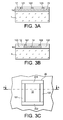
- An optional step may consist in creating, in this layer 12, doped areas N + (or P) 121, 122, 123, as illustrated in Figures 3a and 3b respectively from the structures of Figures 2a and 2b.
- the formation of these doped windows 121, 122, etc., passing right through the layer 12 over its thickness, and which will only dope the indexed areas 121, 122; 123 ... etc, is performed by implantation using a mask implantation.
- zones or windows 121, 122, 123 will allow the subsequent formation of lateral insulation, by preferential oxidation of these same zones or windows. They will also make it possible, in the case of a continuous zone or layer, to carry out the porosification of this zone 15, if this porosification is carried out after formation of the second layer 12.
- the plates then undergo, optionally, an annealing of recrystallization and activation of the implanted dopants: if the implantation N + (to form the layer 15 or the zone 14) generates amorphization of the implanted layer 14, the amorphized zone is annealed at high temperature. Annealing at 1050 ° C for a few seconds may be sufficient for the atoms to diffuse and the amorphous zone to recrystallize. Such a step uses very high speeds of rise and fall in temperature, typically of the order of 80 K / s.
- the thicknesses of the layers 10, 12, 100 and 102 are preferably such that, during the high temperature technological steps that the substrate may possibly have to undergo, before the electrochemical transformation step of the zones 14, 15, these layers do not lose no, or little, their role of "stop layer” vis-à-vis this same transformation.
- the thicknesses of these layers are greater than the diffusion length of the species considered during the high temperature annealing times that they can be subjected to, which length is itself dependent on the temperature, the duration of the annealing, the chemical species that diffuses and the material in which the species diffuses.
- These layers have for example a thickness between 10 nm and 30 nm or 50 nm or 100 nm.
- this length is of the order of 8 nm for a layer 15 or a zone 14 doped at 10 18 atoms / cm 3 and of the order of 22 nm for a layer 15 or a zone 14 doped with 10 21 atoms / cm 3 .
- FIGS. 2a and 2b Other methods for producing the structures illustrated in FIGS. 2a and 2b can be proposed.
- an electrochemical treatment which leads to the transformation, in porous semiconductor material, of the zones 14, 15 located in the first layer 10, can be implemented before the formation of the second layer 12.
- This transformation porous material may for example be made by electrolysis in a solution comprising, at least, hydrofluoric acid.
- the formation of porous silicon is for example explained in the book Properties of Porous Silicon (IEE, EMIS datareview series No. 18, edited by L.Canham, 1997 ).
- the porous Si layer is subsequently oxidized, preferably after any epitaxial step for which the porous silicon is the support (it is sought to maintain the crystalline character for the purpose of epitaxy to give rise to a single crystal, this is the case of porous Si).
- Other materials than silicon can be used, for example SiGe or Ge, with a low temperature recipe for the latter.
- the porosity of the layer transformed by such a process is equal to the ratio of the molar volumes of SiO 2 and silicon, ie of the order of 56%, if it is desired that the oxidation of the silicon remaining after conversion into Si porous is equal to the volume of Si before conversion to porous Si. If the porosity occupies less than 56% (respectively more than 56%) of the initial volume of silicon, the oxide formed will be dense (respectively still porous) and likely to mechanically stress the materials of its environment by putting them in compression. For an upper (or lower) porosity at 0.56, oxidation results in a reduction (or an increase) in volume.
- the porous Si being a crystalline material (which is also the case if using a semiconductor other than Si, for example SiGe or Ge), it can be used as a substrate for epitaxial growth of silicon or another semiconductor material (an alloy of silicon - germanium for example), in order to achieve the layer 12.
- a semiconductor other than Si for example SiGe or Ge
- another semiconductor material an alloy of silicon - germanium for example
- the epitaxial growth of this layer 12 is carried out using equipment such as CVD (Chemical Vapor Deposition) or MBE (Molecular Beam Epitaxy) equipment.
- the growth temperature is below 700 ° C in order to avoid a restructuring of the porous layer; in addition, the deposition rate is relatively high (greater than 1 nm / min) in order to avoid the filling of the open pores of the zones 14 or 15.
- This epitaxy can for example be carried out at 650 ° C. using silane (SiH 4 ) at a pressure of 60 Torr.
- the same electrochemical treatment (which has just been explained above) making it possible to porous the zones 14, 15 can also be carried out after the formation of the second layer 12, by transforming the first layer 10 (which has become buried layer) from implanted windows 121, 122, 123 shown in FIGS. 3a and 3b.
- An advantage is then to have prepared zones for the formation of isolation zones lateral through the areas 121, 122, 123, ... etc which may be oxidized preferentially in the following process. These areas 121, 122, etc. are converted into porous zones at the same time as the zones 13, 15, or before, to allow access to the latter.
- the transformation into insulating zones can take place from the moment when these zones have played their role of epitaxial support.
- FIG. 3a A view from above of the structure illustrated in FIG. 3a can be that of FIG. 3c, in which the zones 121, 122 define two sides of a frame which surrounds a portion of the film 12. Two other sides 221, 222, of same nature as the zones 121, 122, may have been made in the same way as the latter.
- the pattern thus defined in the layer 12 is then surrounded by a box 20 delimited by the edges 121, 122, 221, 222 strongly N + doped.
- Figures 3a and 3b then show sections along the axis AA of Figure 3c.
- the temperature of the following technological steps preferably remains below about 650 ° C., in order to avoid the risk that porous silicon can redensify itself.
- the semiconductor semiconductor ⁇ porous semiconductor transformation is preferably carried out during the step of preparation of the specific substrate (so before formation of the second layer 12), to avoid the loss of selectivity with respect to the electrochemical transformation of the buried layer 12. If the channel is N + or P doped it is capable of being converted into porous Si.
- the doping of the channel 2a can then be done during the epitaxial step of the layer 12 itself, without altering the dense character of the layer 12.
- the epitaxy is made from a surface in which the pores open, it is in ranges of growth rates high enough to obscure these pores without filling them.
- the layer 12 is then a monocrystal respecting the crystalline orientation of the silicon of the layer 10.
- the dose of the doping can be adjusted by the ratio of gas mixtures introduced into the epitaxy chamber. This doping can also be carried out after epitaxy by a standard implantation step.
- Si or SiGe or Ge whether porous or dense, are crystalline. They can therefore be the support for epitaxial growth, each with its own epitaxy conditions: the epitaxial rate on a porous surface, or surface to which the pores open, is chosen high enough to obscure the pores without filling them.
- this zone 14 is still dense (not yet porosified), it is preferably implemented materials that resist the electrochemical step that will subsequently transform the dense semiconductor material into porous semiconductor.
- This electrochemical step may involve a chemical solution containing, inter alia, hydrofluoric acid (FH), the materials likely to be attacked by this solution will preferably be avoided or protected.
- the gate dielectric 3 (FIG. 1) may be formed from a layer 30 made of a high permittivity dielectric material, such as hafnium dioxide (HfO 2 ), or alumina Al 2 O 3 or zirconium oxide ZrO 2 , or in a stack of these materials, rather than SiO 2 .
- the material in contact with the HF will resist this acid (it will be for example HfO 2 ).
- the gate 4 will preferably be obtained from a stack of a TiN layer and a polycrystalline silicon layer (FIG. ). If layer 14 is already porous, the gate oxide may be SiO 2 and the gate may consist only of polycrystalline silicon.
- the spacers 5a, 5b may be formed of Si 3 N 4 nitride and, in this case, the top of the gate 4 is protected by a layer in which the etching of the spacers will stop.
- This layer may itself be a nitride layer and is indexed 60 in FIG. 4, which illustrates the technological stack constructed before the etching of the grid.
- FIG. 5 illustrates the topology of the component after the etching of the gate 4 and the etching of the spacers 5a, 5b.
- the layer or zone 40 is the gate layer (polycrystalline Si or TiN + Si-polycrystalline).
- the layer 60 represents the stop layer or hard mask which remains at the top of the gate in FIG. 5 after etching the spacers: it protects the gate from a subsequent etching step.
- the layer or zone 14 or 15 is already porous, low temperature processes and associated materials are preferably used, preferably avoiding the formation of thermal oxide SiO 2 as a gate dielectric. It is possible, for example, to deposit HfO 2 (at about 650 ° C.) over a few nanometers in thickness to form the layer 30.
- gate dielectric 3 makes it possible to produce a gate stack 3 of a TiN layer and of a polycrystalline silicon layer.
- the spacers 5a, 5b may be formed of a stack of silicon dioxide deposited at low temperature and a silicon nitride silicon deposited also at low temperature.
- the oxide layer 30 then serves as a stop layer for etching the spacers and there is no need for the layer 60 illustrated in FIG. 4.
- FIG. 4 illustrates the architecture that can be implemented before the engraving of the grid while Figure 5 illustrates the configuration obtained after the etchings of the grid 4 and the spacers 5a, 5b, the pedestal oxide 30 being preserved.
- the deposition conditions of the oxide layer 3 and the gate dielectric 30 are preferably selected in order to obscure the pores emerging from these zones 121 - 123 without filling them. . This condition makes it possible to re-access the buried zone 14. If these conditions are not satisfied, these access zones can be cleared by etching located at these access zones 121 - 123 at the buried layer 14.
- This implantation of the layer 12 is intended to form the so-called extension zones of the source and drain, the channel being masked by the grid.
- the implementation conditions will take into account the future thermal budget, so that the layer 12 is not made porous, since it will be the place of electronic transport when the transistor will be functional.
- the implantation profiles are chosen such that, at the stage of the electrochemical transformation semiconductor dense ⁇ porous semiconductor, it remains between the layer 14 and the layer 12 , whose surface layers have just been doped, a zone whose doping is of N type and the dopant concentration is less than 10 17 atoms / cm 3 .
- the layer 12 is thickened so that, in the end, this condition is verified.
- a sequence of steps of masking and removal of the dielectric then makes it possible to access the surface of the lightly doped silicon layer 12 while preserving the dielectric 30 in line with the zones 121 - 123 (if they exist). It is thus possible to define lateral zones 70 and 72 on either side of the spacers, as shown in FIG. 6, on which the etching mask has been removed.
- the etching of the oxide in the zones 70 and 72 is carried out so as not to damage the oxide 6 at the top of the gate 4: a masking of the grid 4 is then made, while the layer 6 illustrated in Figure 5a serves as a natural mask.
- dielectric gate layer 30 serving as a natural mask in the places where it remains.
- This etching is stopped in the layer 15 or 14, as illustrated in FIG. 7 on which are represented the cavities 80 and 82 thus formed on either side of the grid, between the indexed zones 121 and 123.
- a thickness 1 of non-etched semiconductor material 90, 92 located between the cavity and the possible zones 121, 123 may be sized to provide a certain elastic rigidity to the silicon frame which will thus surround the cavities 80 and 82.
- the rectangular geometry of the cavities 80 and 82, visible in FIG. 7, is only indicative: the vertical blanks of these cavities may actually have a certain inclination and / or a certain curvature.
- An epitaxial recovery can then be implemented in the cavities 80 and 82, for example an epitaxy of an alloy 100, 102 of silicon and germanium on the silicon can be carried out: this step leads to the compression of this epitaxial alloy, whose natural mesh parameter is larger than that of silicon or the semiconductor material 14, 15 on which it grows.
- This state of stress of the epitaxial material in the cavities 80 and 82 will affect the stress state of the zone 2a (channel) of the layer 10 which remains under the gate 4.
- the zone in question is put into compression when the overall mechanical equilibrium of the structure is established.
- zones 14 and 15 are in Si, it is possible to use a SiGeC alloy, whose carbon contents are such that the SiGeC mesh parameter is lower than that of the silicon.
- the filling material of cavities 80 and 82 may also be a material with a coefficient of expansion different from that of silicon: when returning to ambient temperature from the temperature at which the material in question is deposited, this material does not shrink. in the same way as the substrate and so it is constrained. It will be compressed (or put in tension) if its coefficient of expansion is lower (or higher) than that the silicon substrate: the channel 2a of the transistor will itself be put into compression (or voltage).
- FIG. 8 illustrates the topology obtained from the state presented in FIG. 7, taking into account an epitaxy step and a step of removing the gate dielectric 30 directly above the access zones. 121 - 123.
- the cavities 80 and 82 can also open into the layer 10 or even into the substrate 1. In this case, the layer 14 or 15 is broken in different non-connected areas. The final function of these zones being to isolate the device from the substrate, they are then made porous (if they are not yet) and then oxidized.
- This oxidation also leads to an oxidation of the bottom and the blanks of the cavities 80, 82, which can be freed of this oxide by a hydrofluoric acid etching step.
- the epitaxial parameters are preferably chosen to block the pores opening at the bottom of the cavities, without filling these pores.
- the dense silicon frame defined by the portions 90, 92 in FIG. 7, makes it possible to surround the epitaxial zones in a more rigid frame. that the frame simply made of porous silicon. The constraint towards the canal of transistor is then transmitted more efficiently. The more these areas 90, 92 have a large width 1, the more the transfer of stress to the channel 2a will be effective.
- the layer or zone 14, 15 is not yet porous, it can be made porous according to the electrochemical method described in the book "Properties of Porous Silicon” already cited here. -above. If the spacers 5a, 5b are a bilayer SiO 2 / Si 3 N 4 , a masking of the grid will avoid the consumption of the oxide during this step. For this reason, nitride spacers 5a, 5b, with protection of the top of the grid by a nitride, are preferable.
- the invention thus makes it possible to obtain a constrained channel device surrounded by a porous silicon box, whatever the moment at which the transformation of the zones 121 - 123 and 14, 15 into porous semiconductor material has been carried out.
- a final oxidation step makes it possible to preferentially oxidize the porous silicon.
- the final structure is that shown in FIG. 9 where the zone 10 is formed of a porous electrical insulator (SiO 2 ) and surrounds a constrained MOS transistor type device. This zone results from the oxidation of the zones 121 - 123 and 14, 15 previously made porous.
- the final structure in section corresponds to that presented in FIG.
- the channel 2a is well constrained and isolated from the substrate by the zone 140, the drain and source areas 100, 102 resting on the substrate.
- the device is particularly interesting for a PMOS type component, since the channel is in compression and that, therefore, the mobility of the holes is increased compared to a unconstrained case.
- this architecture is particularly advantageous for an NMOS-type component, since the voltage channel increases the electron mobility.
- FIG. 11 a schematic view from above of the device thus constructed is illustrated in FIG. 11, FIG. 10 being able to represent a section of this top view taken along the sectional plane BB defined in FIG. 11.
- access to the buried layer 14, 15 can be obtained by an opening in the layer 12, trench called STI for "Shallow trench insulation"". This trench must open into the buried layer 14, 15 to allow its transformation into porous semiconductor material and / or its oxidation.
- the trench can then be filled by an electrical insulator (SiO 2 ).
- SiO 2 electrical insulator
- the material rendered porous during the process has degraded mechanical stiffness relative to the dense material.
- the frame (FIG. 11) formed by the zones 90 and 92 makes it possible to ensure a better transfer of the constraints of the sources and the drain towards the channel (this one is dense). At the end, the insulating material is no longer porous.
- a device and a method according to the invention make it possible to obtain a stress which is exerted over the entire thickness of the channel 2a, which homogenizes the state of constraint of the channel.
Landscapes
- Insulated Gate Type Field-Effect Transistor (AREA)
- Thin Film Transistor (AREA)
Applications Claiming Priority (1)
| Application Number | Priority Date | Filing Date | Title |
|---|---|---|---|
| FR0551664A FR2887370B1 (fr) | 2005-06-17 | 2005-06-17 | Procede de fabrication d'un transistor isole a canal contraint |
Publications (3)
| Publication Number | Publication Date |
|---|---|
| EP1734568A2 true EP1734568A2 (de) | 2006-12-20 |
| EP1734568A3 EP1734568A3 (de) | 2009-12-09 |
| EP1734568B1 EP1734568B1 (de) | 2015-10-14 |
Family
ID=35539486
Family Applications (1)
| Application Number | Title | Priority Date | Filing Date |
|---|---|---|---|
| EP06115549.5A Not-in-force EP1734568B1 (de) | 2005-06-17 | 2006-06-15 | Isolierter Transistor mit einem verspannten Kanal und Herstellungsverfahren |
Country Status (3)
| Country | Link |
|---|---|
| US (1) | US7635615B2 (de) |
| EP (1) | EP1734568B1 (de) |
| FR (1) | FR2887370B1 (de) |
Cited By (3)
| Publication number | Priority date | Publication date | Assignee | Title |
|---|---|---|---|---|
| WO2007053382A1 (en) * | 2005-10-31 | 2007-05-10 | Advanced Micro Devices, Inc. | An embedded strain layer in thin soi transistors and a method of forming the same |
| US7399663B2 (en) | 2005-10-31 | 2008-07-15 | Advanced Micro Devices, Inc. | Embedded strain layer in thin SOI transistors and a method of forming the same |
| KR20180127333A (ko) * | 2016-04-01 | 2018-11-28 | 인텔 코포레이션 | 열 성능 부스트를 갖는 트랜지스터 |
Families Citing this family (4)
| Publication number | Priority date | Publication date | Assignee | Title |
|---|---|---|---|---|
| US7569434B2 (en) * | 2006-01-19 | 2009-08-04 | International Business Machines Corporation | PFETs and methods of manufacturing the same |
| FR2921754B1 (fr) * | 2007-09-28 | 2009-11-27 | Stmicroelectronics Crolles Sas | Procede de fabrication d'un subtrat semiconducteur localise sur une couche isolante |
| US8652929B2 (en) * | 2011-12-23 | 2014-02-18 | Peking University | CMOS device for reducing charge sharing effect and fabrication method thereof |
| TW202113928A (zh) * | 2019-06-06 | 2021-04-01 | 英商Iqe有限公司 | 分層結構中的可調應力補償 |
Family Cites Families (14)
| Publication number | Priority date | Publication date | Assignee | Title |
|---|---|---|---|---|
| US4104090A (en) * | 1977-02-24 | 1978-08-01 | International Business Machines Corporation | Total dielectric isolation utilizing a combination of reactive ion etching, anodic etching, and thermal oxidation |
| JP2762215B2 (ja) * | 1993-08-12 | 1998-06-04 | 株式会社半導体エネルギー研究所 | 薄膜トランジスタおよび半導体装置の作製方法 |
| FR2779006B1 (fr) * | 1998-05-19 | 2003-01-24 | St Microelectronics Sa | Procede de formation de silicium poreux dans un substrat de silicium, en particulier pour l'amelioration des performances d'un circuit inductif |
| JP2002043576A (ja) * | 2000-07-24 | 2002-02-08 | Univ Tohoku | 半導体装置 |
| US6541356B2 (en) * | 2001-05-21 | 2003-04-01 | International Business Machines Corporation | Ultimate SIMOX |
| US6621131B2 (en) * | 2001-11-01 | 2003-09-16 | Intel Corporation | Semiconductor transistor having a stressed channel |
| FR2838237B1 (fr) | 2002-04-03 | 2005-02-25 | St Microelectronics Sa | Procede de fabrication d'un transistor a effet de champ a grille isolee a canal contraint et circuit integre comprenant un tel transistor |
| US7074623B2 (en) * | 2002-06-07 | 2006-07-11 | Amberwave Systems Corporation | Methods of forming strained-semiconductor-on-insulator finFET device structures |
| US6717216B1 (en) * | 2002-12-12 | 2004-04-06 | International Business Machines Corporation | SOI based field effect transistor having a compressive film in undercut area under the channel and a method of making the device |
| WO2004073043A2 (en) * | 2003-02-13 | 2004-08-26 | Massachusetts Institute Of Technology | Semiconductor-on-insulator article and method of making same |
| US6909186B2 (en) * | 2003-05-01 | 2005-06-21 | International Business Machines Corporation | High performance FET devices and methods therefor |
| TWI242232B (en) * | 2003-06-09 | 2005-10-21 | Canon Kk | Semiconductor substrate, semiconductor device, and method of manufacturing the same |
| JP2007500936A (ja) * | 2003-07-31 | 2007-01-18 | アドバンスト・マイクロ・ディバイシズ・インコーポレイテッド | ゲートの枯渇を低減した注入ゲート電極を有する電界効果型トランジスタ、及び、このトランジスタを製造する方法 |
| US6939751B2 (en) * | 2003-10-22 | 2005-09-06 | International Business Machines Corporation | Method and manufacture of thin silicon on insulator (SOI) with recessed channel |
-
2005
- 2005-06-17 FR FR0551664A patent/FR2887370B1/fr not_active Expired - Fee Related
-
2006
- 2006-06-15 EP EP06115549.5A patent/EP1734568B1/de not_active Not-in-force
- 2006-06-16 US US11/454,398 patent/US7635615B2/en not_active Expired - Fee Related
Cited By (3)
| Publication number | Priority date | Publication date | Assignee | Title |
|---|---|---|---|---|
| WO2007053382A1 (en) * | 2005-10-31 | 2007-05-10 | Advanced Micro Devices, Inc. | An embedded strain layer in thin soi transistors and a method of forming the same |
| US7399663B2 (en) | 2005-10-31 | 2008-07-15 | Advanced Micro Devices, Inc. | Embedded strain layer in thin SOI transistors and a method of forming the same |
| KR20180127333A (ko) * | 2016-04-01 | 2018-11-28 | 인텔 코포레이션 | 열 성능 부스트를 갖는 트랜지스터 |
Also Published As
| Publication number | Publication date |
|---|---|
| EP1734568A3 (de) | 2009-12-09 |
| FR2887370A1 (fr) | 2006-12-22 |
| US20070001227A1 (en) | 2007-01-04 |
| EP1734568B1 (de) | 2015-10-14 |
| FR2887370B1 (fr) | 2007-12-28 |
| US7635615B2 (en) | 2009-12-22 |
Similar Documents
| Publication | Publication Date | Title |
|---|---|---|
| EP1837916B1 (de) | Verfahren zum Herstellen eines Transistors mit einem Germanium enthaltenden Kanal | |
| EP2075826B1 (de) | Verfahren zur Herstellung eines Halbleiter-auf-Isolator-Substrats, das eine Anreicherungsetappe mit lokalisiertem Germanium umfasst | |
| FR2795554A1 (fr) | Procede de gravure laterale par trous pour fabriquer des dis positifs semi-conducteurs | |
| FR2838237A1 (fr) | Procede de fabrication d'un transistor a effet de champ a grille isolee a canal contraint et circuit integre comprenant un tel transistor | |
| FR2821483A1 (fr) | Procede de fabrication d'un transistor a grille isolee et a architecture du type substrat sur isolant, et transistor correspondant | |
| FR3060850A1 (fr) | Procede de fabrication d’un transistor a nanocouches a canal vertical | |
| EP3261124B1 (de) | Verfahren zur bildung von abstandhaltern eines gates eines transistors | |
| EP2610915A1 (de) | Transistor und Herstellungsverfahren eines Transistors | |
| FR3019373A1 (fr) | Procede de fabrication d'une plaque de semi-conducteur adaptee pour la fabrication d'un substrat soi et plaque de substrat ainsi obtenue | |
| EP3142151B1 (de) | Herstellungsverfahren einer einachsig verspannten transistorkanalstruktur | |
| FR3005372A1 (fr) | Procede de realisation d'un film en silicium-germanium a teneur en germanium variable | |
| FR2860919A1 (fr) | Structures et procedes de fabrication de regions semiconductrices sur isolant | |
| EP3503175A1 (de) | Herstellungsverfahren eines halbleitersubstrats mit mindestens einem unter druckspannung stehenden halbleiterbereich | |
| EP1734568B1 (de) | Isolierter Transistor mit einem verspannten Kanal und Herstellungsverfahren | |
| FR3088481A1 (fr) | Procede de fabrication d’un transistor a effet de champ a jonction alignee avec des espaceurs | |
| EP1638149A2 (de) | Verfahren zur Herstellung eines Feldefekttransistors mit isoliertem Gatter und Heterostruktur-Kanal und entsprechender Transistor | |
| EP1788635B1 (de) | Verfahren zum Herstellen eines Transistors mit selbst justierten Doppel-Gates durch Schrumpfung der Gatestruktur | |
| EP2562803B1 (de) | Herstellungsverfahren für ein Bauelement mit mit Hilfe einer externen Schicht verspannten Transistoren, und Bauelement | |
| FR3046492A1 (fr) | Procede de realisation de transistors mos contraints | |
| FR3048815A1 (fr) | Procede de co-realisation de zones sous contraintes uniaxiales differentes | |
| EP3667715B1 (de) | Verfahren zur herstellung eines halbleitersubstrates mit einem verspannten halbleitergebiet | |
| EP3671826B1 (de) | Verbessertes herstellungsverfahren eines integrierten schaltkreises, der einen nmos- und einen pmos-transistor umfasst | |
| EP3961721A1 (de) | Verbessertes verfahren zur germaniumanreicherung um den kanal eines transistors | |
| EP3961720B1 (de) | Germaniumanreicherung um den kanal herum durch erhöhte blöcke | |
| EP3035386B1 (de) | Herstellungsverfahren einer verbesserten feldeffektvorrichtung |
Legal Events
| Date | Code | Title | Description |
|---|---|---|---|
| PUAI | Public reference made under article 153(3) epc to a published international application that has entered the european phase |
Free format text: ORIGINAL CODE: 0009012 |
|
| AK | Designated contracting states |
Kind code of ref document: A2 Designated state(s): AT BE BG CH CY CZ DE DK EE ES FI FR GB GR HU IE IS IT LI LT LU LV MC NL PL PT RO SE SI SK TR |
|
| AX | Request for extension of the european patent |
Extension state: AL BA HR MK YU |
|
| PUAL | Search report despatched |
Free format text: ORIGINAL CODE: 0009013 |
|
| AK | Designated contracting states |
Kind code of ref document: A3 Designated state(s): AT BE BG CH CY CZ DE DK EE ES FI FR GB GR HU IE IS IT LI LT LU LV MC NL PL PT RO SE SI SK TR |
|
| AX | Request for extension of the european patent |
Extension state: AL BA HR MK RS |
|
| RAP1 | Party data changed (applicant data changed or rights of an application transferred) |
Owner name: STMICROELECTRONICS (CROLLES 2) SAS Owner name: COMMISSARIAT A L'ENERGIE ATOMIQUE ET AUX ENERGIES |
|
| 17P | Request for examination filed |
Effective date: 20100607 |
|
| 17Q | First examination report despatched |
Effective date: 20100705 |
|
| AKX | Designation fees paid |
Designated state(s): AT BE BG CH CY CZ DE DK EE ES FI FR GB GR HU IE IS IT LI LT LU LV MC NL PL PT RO SE SI SK TR |
|
| GRAP | Despatch of communication of intention to grant a patent |
Free format text: ORIGINAL CODE: EPIDOSNIGR1 |
|
| INTG | Intention to grant announced |
Effective date: 20150508 |
|
| RIN1 | Information on inventor provided before grant (corrected) |
Inventor name: BARBE, JEAN-CHARLES Inventor name: GALLON, CLAIRE Inventor name: BARRAUD, SYLVAIN Inventor name: FENOUILLET-BERANGER, CLAIRE Inventor name: HALIMAOUI, AOMAR |
|
| GRAS | Grant fee paid |
Free format text: ORIGINAL CODE: EPIDOSNIGR3 |
|
| GRAA | (expected) grant |
Free format text: ORIGINAL CODE: 0009210 |
|
| AK | Designated contracting states |
Kind code of ref document: B1 Designated state(s): AT BE BG CH CY CZ DE DK EE ES FI FR GB GR HU IE IS IT LI LT LU LV MC NL PL PT RO SE SI SK TR |
|
| REG | Reference to a national code |
Ref country code: GB Ref legal event code: FG4D Free format text: NOT ENGLISH |
|
| REG | Reference to a national code |
Ref country code: AT Ref legal event code: REF Ref document number: 755683 Country of ref document: AT Kind code of ref document: T Effective date: 20151015 Ref country code: CH Ref legal event code: EP |
|
| REG | Reference to a national code |
Ref country code: IE Ref legal event code: FG4D Free format text: LANGUAGE OF EP DOCUMENT: FRENCH |
|
| REG | Reference to a national code |
Ref country code: DE Ref legal event code: R096 Ref document number: 602006046907 Country of ref document: DE |
|
| REG | Reference to a national code |
Ref country code: NL Ref legal event code: MP Effective date: 20151014 |
|
| REG | Reference to a national code |
Ref country code: LT Ref legal event code: MG4D |
|
| REG | Reference to a national code |
Ref country code: AT Ref legal event code: MK05 Ref document number: 755683 Country of ref document: AT Kind code of ref document: T Effective date: 20151014 |
|
| PG25 | Lapsed in a contracting state [announced via postgrant information from national office to epo] |
Ref country code: NL Free format text: LAPSE BECAUSE OF FAILURE TO SUBMIT A TRANSLATION OF THE DESCRIPTION OR TO PAY THE FEE WITHIN THE PRESCRIBED TIME-LIMIT Effective date: 20151014 Ref country code: IT Free format text: LAPSE BECAUSE OF FAILURE TO SUBMIT A TRANSLATION OF THE DESCRIPTION OR TO PAY THE FEE WITHIN THE PRESCRIBED TIME-LIMIT Effective date: 20151014 Ref country code: LT Free format text: LAPSE BECAUSE OF FAILURE TO SUBMIT A TRANSLATION OF THE DESCRIPTION OR TO PAY THE FEE WITHIN THE PRESCRIBED TIME-LIMIT Effective date: 20151014 Ref country code: ES Free format text: LAPSE BECAUSE OF FAILURE TO SUBMIT A TRANSLATION OF THE DESCRIPTION OR TO PAY THE FEE WITHIN THE PRESCRIBED TIME-LIMIT Effective date: 20151014 Ref country code: IS Free format text: LAPSE BECAUSE OF FAILURE TO SUBMIT A TRANSLATION OF THE DESCRIPTION OR TO PAY THE FEE WITHIN THE PRESCRIBED TIME-LIMIT Effective date: 20160214 |
|
| PG25 | Lapsed in a contracting state [announced via postgrant information from national office to epo] |
Ref country code: PT Free format text: LAPSE BECAUSE OF FAILURE TO SUBMIT A TRANSLATION OF THE DESCRIPTION OR TO PAY THE FEE WITHIN THE PRESCRIBED TIME-LIMIT Effective date: 20160215 Ref country code: PL Free format text: LAPSE BECAUSE OF FAILURE TO SUBMIT A TRANSLATION OF THE DESCRIPTION OR TO PAY THE FEE WITHIN THE PRESCRIBED TIME-LIMIT Effective date: 20151014 Ref country code: LV Free format text: LAPSE BECAUSE OF FAILURE TO SUBMIT A TRANSLATION OF THE DESCRIPTION OR TO PAY THE FEE WITHIN THE PRESCRIBED TIME-LIMIT Effective date: 20151014 Ref country code: FI Free format text: LAPSE BECAUSE OF FAILURE TO SUBMIT A TRANSLATION OF THE DESCRIPTION OR TO PAY THE FEE WITHIN THE PRESCRIBED TIME-LIMIT Effective date: 20151014 Ref country code: AT Free format text: LAPSE BECAUSE OF FAILURE TO SUBMIT A TRANSLATION OF THE DESCRIPTION OR TO PAY THE FEE WITHIN THE PRESCRIBED TIME-LIMIT Effective date: 20151014 Ref country code: GR Free format text: LAPSE BECAUSE OF FAILURE TO SUBMIT A TRANSLATION OF THE DESCRIPTION OR TO PAY THE FEE WITHIN THE PRESCRIBED TIME-LIMIT Effective date: 20160115 Ref country code: SE Free format text: LAPSE BECAUSE OF FAILURE TO SUBMIT A TRANSLATION OF THE DESCRIPTION OR TO PAY THE FEE WITHIN THE PRESCRIBED TIME-LIMIT Effective date: 20151014 |
|
| REG | Reference to a national code |
Ref country code: FR Ref legal event code: PLFP Year of fee payment: 11 |
|
| REG | Reference to a national code |
Ref country code: DE Ref legal event code: R097 Ref document number: 602006046907 Country of ref document: DE |
|
| PG25 | Lapsed in a contracting state [announced via postgrant information from national office to epo] |
Ref country code: CZ Free format text: LAPSE BECAUSE OF FAILURE TO SUBMIT A TRANSLATION OF THE DESCRIPTION OR TO PAY THE FEE WITHIN THE PRESCRIBED TIME-LIMIT Effective date: 20151014 |
|
| PLBE | No opposition filed within time limit |
Free format text: ORIGINAL CODE: 0009261 |
|
| STAA | Information on the status of an ep patent application or granted ep patent |
Free format text: STATUS: NO OPPOSITION FILED WITHIN TIME LIMIT |
|
| PG25 | Lapsed in a contracting state [announced via postgrant information from national office to epo] |
Ref country code: RO Free format text: LAPSE BECAUSE OF FAILURE TO SUBMIT A TRANSLATION OF THE DESCRIPTION OR TO PAY THE FEE WITHIN THE PRESCRIBED TIME-LIMIT Effective date: 20151014 Ref country code: EE Free format text: LAPSE BECAUSE OF FAILURE TO SUBMIT A TRANSLATION OF THE DESCRIPTION OR TO PAY THE FEE WITHIN THE PRESCRIBED TIME-LIMIT Effective date: 20151014 Ref country code: DK Free format text: LAPSE BECAUSE OF FAILURE TO SUBMIT A TRANSLATION OF THE DESCRIPTION OR TO PAY THE FEE WITHIN THE PRESCRIBED TIME-LIMIT Effective date: 20151014 Ref country code: SK Free format text: LAPSE BECAUSE OF FAILURE TO SUBMIT A TRANSLATION OF THE DESCRIPTION OR TO PAY THE FEE WITHIN THE PRESCRIBED TIME-LIMIT Effective date: 20151014 |
|
| 26N | No opposition filed |
Effective date: 20160715 |
|
| PG25 | Lapsed in a contracting state [announced via postgrant information from national office to epo] |
Ref country code: SI Free format text: LAPSE BECAUSE OF FAILURE TO SUBMIT A TRANSLATION OF THE DESCRIPTION OR TO PAY THE FEE WITHIN THE PRESCRIBED TIME-LIMIT Effective date: 20151014 |
|
| PG25 | Lapsed in a contracting state [announced via postgrant information from national office to epo] |
Ref country code: BE Free format text: LAPSE BECAUSE OF NON-PAYMENT OF DUE FEES Effective date: 20160630 |
|
| REG | Reference to a national code |
Ref country code: DE Ref legal event code: R119 Ref document number: 602006046907 Country of ref document: DE |
|
| PG25 | Lapsed in a contracting state [announced via postgrant information from national office to epo] |
Ref country code: MC Free format text: LAPSE BECAUSE OF FAILURE TO SUBMIT A TRANSLATION OF THE DESCRIPTION OR TO PAY THE FEE WITHIN THE PRESCRIBED TIME-LIMIT Effective date: 20151014 |
|
| REG | Reference to a national code |
Ref country code: CH Ref legal event code: PL |
|
| GBPC | Gb: european patent ceased through non-payment of renewal fee |
Effective date: 20160615 |
|
| REG | Reference to a national code |
Ref country code: IE Ref legal event code: MM4A |
|
| PG25 | Lapsed in a contracting state [announced via postgrant information from national office to epo] |
Ref country code: LI Free format text: LAPSE BECAUSE OF NON-PAYMENT OF DUE FEES Effective date: 20160630 Ref country code: DE Free format text: LAPSE BECAUSE OF NON-PAYMENT OF DUE FEES Effective date: 20170103 Ref country code: CH Free format text: LAPSE BECAUSE OF NON-PAYMENT OF DUE FEES Effective date: 20160630 |
|
| PG25 | Lapsed in a contracting state [announced via postgrant information from national office to epo] |
Ref country code: IE Free format text: LAPSE BECAUSE OF NON-PAYMENT OF DUE FEES Effective date: 20160615 Ref country code: GB Free format text: LAPSE BECAUSE OF NON-PAYMENT OF DUE FEES Effective date: 20160615 |
|
| REG | Reference to a national code |
Ref country code: FR Ref legal event code: PLFP Year of fee payment: 12 |
|
| PG25 | Lapsed in a contracting state [announced via postgrant information from national office to epo] |
Ref country code: CY Free format text: LAPSE BECAUSE OF FAILURE TO SUBMIT A TRANSLATION OF THE DESCRIPTION OR TO PAY THE FEE WITHIN THE PRESCRIBED TIME-LIMIT Effective date: 20151014 Ref country code: HU Free format text: LAPSE BECAUSE OF FAILURE TO SUBMIT A TRANSLATION OF THE DESCRIPTION OR TO PAY THE FEE WITHIN THE PRESCRIBED TIME-LIMIT; INVALID AB INITIO Effective date: 20060615 |
|
| REG | Reference to a national code |
Ref country code: FR Ref legal event code: PLFP Year of fee payment: 13 |
|
| PG25 | Lapsed in a contracting state [announced via postgrant information from national office to epo] |
Ref country code: LU Free format text: LAPSE BECAUSE OF NON-PAYMENT OF DUE FEES Effective date: 20160615 Ref country code: TR Free format text: LAPSE BECAUSE OF FAILURE TO SUBMIT A TRANSLATION OF THE DESCRIPTION OR TO PAY THE FEE WITHIN THE PRESCRIBED TIME-LIMIT Effective date: 20151014 |
|
| PG25 | Lapsed in a contracting state [announced via postgrant information from national office to epo] |
Ref country code: BG Free format text: LAPSE BECAUSE OF FAILURE TO SUBMIT A TRANSLATION OF THE DESCRIPTION OR TO PAY THE FEE WITHIN THE PRESCRIBED TIME-LIMIT Effective date: 20151014 |
|
| PGFP | Annual fee paid to national office [announced via postgrant information from national office to epo] |
Ref country code: FR Payment date: 20200630 Year of fee payment: 15 |
|
| PG25 | Lapsed in a contracting state [announced via postgrant information from national office to epo] |
Ref country code: FR Free format text: LAPSE BECAUSE OF NON-PAYMENT OF DUE FEES Effective date: 20210630 |