EP1732117A2 - Semiconductor device packaging substrate and semiconductor device packaging structure - Google Patents
Semiconductor device packaging substrate and semiconductor device packaging structure Download PDFInfo
- Publication number
- EP1732117A2 EP1732117A2 EP06011898A EP06011898A EP1732117A2 EP 1732117 A2 EP1732117 A2 EP 1732117A2 EP 06011898 A EP06011898 A EP 06011898A EP 06011898 A EP06011898 A EP 06011898A EP 1732117 A2 EP1732117 A2 EP 1732117A2
- Authority
- EP
- European Patent Office
- Prior art keywords
- packaging substrate
- underfill resin
- semiconductor device
- opening portion
- solder resist
- Prior art date
- Legal status (The legal status is an assumption and is not a legal conclusion. Google has not performed a legal analysis and makes no representation as to the accuracy of the status listed.)
- Withdrawn
Links
Images







Classifications
-
- H—ELECTRICITY
- H10—SEMICONDUCTOR DEVICES; ELECTRIC SOLID-STATE DEVICES NOT OTHERWISE PROVIDED FOR
- H10W—GENERIC PACKAGES, INTERCONNECTIONS, CONNECTORS OR OTHER CONSTRUCTIONAL DETAILS OF DEVICES COVERED BY CLASS H10
- H10W72/00—Interconnections or connectors in packages
- H10W72/30—Die-attach connectors
-
- H—ELECTRICITY
- H10—SEMICONDUCTOR DEVICES; ELECTRIC SOLID-STATE DEVICES NOT OTHERWISE PROVIDED FOR
- H10W—GENERIC PACKAGES, INTERCONNECTIONS, CONNECTORS OR OTHER CONSTRUCTIONAL DETAILS OF DEVICES COVERED BY CLASS H10
- H10W70/00—Package substrates; Interposers; Redistribution layers [RDL]
- H10W70/60—Insulating or insulated package substrates; Interposers; Redistribution layers
- H10W70/67—Insulating or insulated package substrates; Interposers; Redistribution layers characterised by their insulating layers or insulating parts
- H10W70/69—Insulating materials thereof
-
- H—ELECTRICITY
- H10—SEMICONDUCTOR DEVICES; ELECTRIC SOLID-STATE DEVICES NOT OTHERWISE PROVIDED FOR
- H10W—GENERIC PACKAGES, INTERCONNECTIONS, CONNECTORS OR OTHER CONSTRUCTIONAL DETAILS OF DEVICES COVERED BY CLASS H10
- H10W74/00—Encapsulations, e.g. protective coatings
- H10W74/01—Manufacture or treatment
- H10W74/012—Manufacture or treatment of encapsulations on active surfaces of flip-chip devices, e.g. forming underfills
-
- H—ELECTRICITY
- H10—SEMICONDUCTOR DEVICES; ELECTRIC SOLID-STATE DEVICES NOT OTHERWISE PROVIDED FOR
- H10W—GENERIC PACKAGES, INTERCONNECTIONS, CONNECTORS OR OTHER CONSTRUCTIONAL DETAILS OF DEVICES COVERED BY CLASS H10
- H10W74/00—Encapsulations, e.g. protective coatings
- H10W74/10—Encapsulations, e.g. protective coatings characterised by their shape or disposition
- H10W74/15—Encapsulations, e.g. protective coatings characterised by their shape or disposition on active surfaces of flip-chip devices, e.g. underfills
-
- H—ELECTRICITY
- H10—SEMICONDUCTOR DEVICES; ELECTRIC SOLID-STATE DEVICES NOT OTHERWISE PROVIDED FOR
- H10W—GENERIC PACKAGES, INTERCONNECTIONS, CONNECTORS OR OTHER CONSTRUCTIONAL DETAILS OF DEVICES COVERED BY CLASS H10
- H10W72/00—Interconnections or connectors in packages
- H10W72/071—Connecting or disconnecting
- H10W72/072—Connecting or disconnecting of bump connectors
-
- H—ELECTRICITY
- H10—SEMICONDUCTOR DEVICES; ELECTRIC SOLID-STATE DEVICES NOT OTHERWISE PROVIDED FOR
- H10W—GENERIC PACKAGES, INTERCONNECTIONS, CONNECTORS OR OTHER CONSTRUCTIONAL DETAILS OF DEVICES COVERED BY CLASS H10
- H10W72/00—Interconnections or connectors in packages
- H10W72/071—Connecting or disconnecting
- H10W72/073—Connecting or disconnecting of die-attach connectors
-
- H—ELECTRICITY
- H10—SEMICONDUCTOR DEVICES; ELECTRIC SOLID-STATE DEVICES NOT OTHERWISE PROVIDED FOR
- H10W—GENERIC PACKAGES, INTERCONNECTIONS, CONNECTORS OR OTHER CONSTRUCTIONAL DETAILS OF DEVICES COVERED BY CLASS H10
- H10W72/00—Interconnections or connectors in packages
- H10W72/851—Dispositions of multiple connectors or interconnections
- H10W72/853—On the same surface
- H10W72/856—Bump connectors and die-attach connectors
-
- H—ELECTRICITY
- H10—SEMICONDUCTOR DEVICES; ELECTRIC SOLID-STATE DEVICES NOT OTHERWISE PROVIDED FOR
- H10W—GENERIC PACKAGES, INTERCONNECTIONS, CONNECTORS OR OTHER CONSTRUCTIONAL DETAILS OF DEVICES COVERED BY CLASS H10
- H10W72/00—Interconnections or connectors in packages
- H10W72/90—Bond pads, in general
-
- H—ELECTRICITY
- H10—SEMICONDUCTOR DEVICES; ELECTRIC SOLID-STATE DEVICES NOT OTHERWISE PROVIDED FOR
- H10W—GENERIC PACKAGES, INTERCONNECTIONS, CONNECTORS OR OTHER CONSTRUCTIONAL DETAILS OF DEVICES COVERED BY CLASS H10
- H10W72/00—Interconnections or connectors in packages
- H10W72/90—Bond pads, in general
- H10W72/921—Structures or relative sizes of bond pads
- H10W72/923—Bond pads having multiple stacked layers
-
- H—ELECTRICITY
- H10—SEMICONDUCTOR DEVICES; ELECTRIC SOLID-STATE DEVICES NOT OTHERWISE PROVIDED FOR
- H10W—GENERIC PACKAGES, INTERCONNECTIONS, CONNECTORS OR OTHER CONSTRUCTIONAL DETAILS OF DEVICES COVERED BY CLASS H10
- H10W72/00—Interconnections or connectors in packages
- H10W72/90—Bond pads, in general
- H10W72/941—Dispositions of bond pads
- H10W72/9415—Dispositions of bond pads relative to the surface, e.g. recessed, protruding
-
- H—ELECTRICITY
- H10—SEMICONDUCTOR DEVICES; ELECTRIC SOLID-STATE DEVICES NOT OTHERWISE PROVIDED FOR
- H10W—GENERIC PACKAGES, INTERCONNECTIONS, CONNECTORS OR OTHER CONSTRUCTIONAL DETAILS OF DEVICES COVERED BY CLASS H10
- H10W90/00—Package configurations
- H10W90/701—Package configurations characterised by the relative positions of pads or connectors relative to package parts
- H10W90/721—Package configurations characterised by the relative positions of pads or connectors relative to package parts of bump connectors
- H10W90/724—Package configurations characterised by the relative positions of pads or connectors relative to package parts of bump connectors between a chip and a stacked insulating package substrate, interposer or RDL
-
- H—ELECTRICITY
- H10—SEMICONDUCTOR DEVICES; ELECTRIC SOLID-STATE DEVICES NOT OTHERWISE PROVIDED FOR
- H10W—GENERIC PACKAGES, INTERCONNECTIONS, CONNECTORS OR OTHER CONSTRUCTIONAL DETAILS OF DEVICES COVERED BY CLASS H10
- H10W90/00—Package configurations
- H10W90/701—Package configurations characterised by the relative positions of pads or connectors relative to package parts
- H10W90/731—Package configurations characterised by the relative positions of pads or connectors relative to package parts of die-attach connectors
- H10W90/734—Package configurations characterised by the relative positions of pads or connectors relative to package parts of die-attach connectors between a chip and a stacked insulating package substrate, interposer or RDL
Definitions
- the present invention relates to a semiconductor device packaging substrate and a semiconductor device packaging structure, and more particularly, a semiconductor device packaging substrate and a semiconductor device packaging structure in which an underfill resin is filled between the packaging substrate and a semiconductor device mounted to the packaging substrate in flip-chip bonding.
- the semiconductor device As a method of packaging a semiconductor device which is high in density onto a packaging substrate, flip-chip bonding is used frequently. According to this flip-chip bonding, the semiconductor device is mounted by providing solder bumps on the bottom surface of the semiconductor device as external connection terminals, then setting this semiconductor device in a face-down state to the packaging substrate, and then bonding the solder bumps to electrodes formed on the packaging substrate.
- FIG.1 shows an example of a packaging substrate 1 on which a semiconductor device (semiconductor element) 5 is mounted by the flip-chip bonding in the related art.
- a semiconductor device semiconductor element
- FIG.1 an example in which the semiconductor device 5, such as DRAM, having a center pad structure is mounted on the packaging substrate 1 is shown.
- the packaging substrate 1 is a printed-wiring board, and predetermined wiring patterns, electrodes, etc. are formed on its surface. Also, a solder resist 2 for protecting the wiring patterns, the electrodes, etc. is provided on the surface of the packaging substrate 1.
- the solder resist 2 is a resin that has insulating performance and also has a function of preventing adhesion of the solder.
- An opening portion 3 is formed in a portion, in which the electrodes to be bonded to the solder bumps formed on the semiconductor device 5 are formed, of a packaging area 6 of the solder resist 2, in which the semiconductor device 5 is mounted. Therefore, the electrodes (not shown) bonded to the bumps formed on the packaging substrate 1 are exposed to the outside via the opening portion 3.
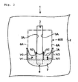
- FIG.2 is a plan view showing a process of providing the underfill resin 7 between the packaging substrate 1 and the semiconductor device 5. Because the underfill resin 7 is provided between the packaging substrate 1 and the semiconductor device 5, illustration of the semiconductor device 5 is omitted herein and only its packaging area 6 is illustrated, for convenience of illustration.
- a liquid underfill resin 7 is injected between the packaging substrate 1 and the semiconductor device 5 from an injection starting position 9.
- the injection starting position 9 is set in a position of the bottom portion of the opening portion 3 in FIG.2.
- the underfill resin 7 when injected from the injection starting position 9 flows upward in FIG.2 to spread into a space between the packaging substrate 1 and the semiconductor device 5.
- a flow end surface 7A as a top end portion of the underfill resin 7 is not formed as a linear end but a curved end shown in FIG.2. This is caused due to the fact that a flow speed of the liquid underfill resin 7 in areas that are located along edge portions 3A of the opening portion 3 and outer peripheral portions 6A of the semiconductor device 5 is higher than that in other areas. More concretely, a flow speed V2 at the edge portion 3A and a flow speed V3 at the outer peripheral portion 6A is higher than a flow speed of the underfill resin 7 on the solder resist 2 indicated with an arrow V1 in FIG.2 (V1 ⁇ V2, V1 ⁇ V3).
- FIG.4 shows an example in which two opening portions 3, 4 are formed in the solder resist 2 to mount the semiconductor device having the pad structure in two rows.
- the opening portions 3, 4 are formed in parallel and then the underfill resin 7 is injected in the direction that is perpendicular to the opening portions 3, 4, particularly the underfill resin 7 goes around fast conspicuously.
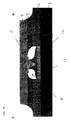
- FIG. 6A shows an SAT (Scanning Acoustic Tomography) image in which voids 8 are generated in the inside of the underfill resin 7 when the underfill resin 7 is injected between the packaging substrate 1 and the semiconductor device 5 as the first related art.
- FIG. 6B shows an image when surface grinding is performed in the state shown in FIG. 6A.
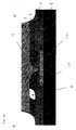
- FIG. 6C is a cross-sectional view of a semiconductor device packaging structure along the line A-A' of FIG. 6A.
- an Au stud bump 11 formed on the semiconductor device 5 and a substrate conductor (electrode) 13 formed on the packaging substrate 1 is connected via a solder 12.
- voids are not generated.
- FIG. 6D is a cross-sectional view of the semiconductor device packaging structure along the line B-B' of FIG. 6A.
- the void 8 is generated in the inside of the underfill resin 7 around the solder 12 between the semiconductor device 5 and the packaging substrate 1.
- FIG. 6E is a cross-sectional view of the semiconductor device packaging structure along the line C-C' of FIG. 6A.
- the void 8 is generated in the inside of the underfill resin 7 above the packaging substrate 1 between the semiconductor device 5 and the packaging substrate 1.
- the present invention has been made in view of the above circumstances, and provides a semiconductor device packaging substrate and a semiconductor device packaging structure, capable of preventing generation of voids in an underfill resin.
- a packaging substrate of the invention for a semiconductor device comprises:
- the underfill resin moves over the adjusting section and is filled between the semiconductor device and the semiconductor device packaging substrate when providing the underfill resin.
- the adjusting section adjusts a flow speed of the underfill resin, the underfill resin can move uniformly and also generation of the voids in the underfill resin can be prevented.
- the adjusting section includes a second opening portion formed in the solder resist.
- the adjusting section is formed by the second opening portion formed in the solder resist, such adjusting section can be formed simultaneously with the first opening portion, and thus the adjusting section can be formed easily.
- the adjusting section includes a convex portion formed on the solder resist.
- the adjusting section is formed by the convex portion formed on the solder resist, such adjusting section can be formed simultaneously when the solder resist is formed, and thus the adjusting section can be formed easily.
- the adjusting section is rectangular-shaped when viewed from a top.
- the adjusting section is shaped into a rectangular shape as a simple shape, the formation of the adjusting section can be executed simply.
- the adjusting section is polygonal-shaped when viewed from a top.
- the adjusting section is shaped into a polygonal shape, a flow speed of the underfill resin can be decreased largely with a small space.
- the adjusting section is provided on one side of the first opening portion, the side that is opposite to an injection starting position of the underfill resin.
- the adjusting section is formed in a position partially covering an outer periphery of a region in which the semiconductor device is mounted.
- the underfill resin can be provided in further uniform state.
- a packaging structure of the invention comprises:
- the underfill resin moves over the adjusting section when providing the underfill resin, the flow speed is adjusted and therefore generation of the voids in the underfill resin can be prevented. Also, since the underfill resin is provided in the region including the adjusting section, after the underfill resin is provided, the underfill resin can be secured without fail on the semiconductor device packaging substrate by an anchor effect of the adjusting section.
- the adjusting section adjusts the flow speed of the underfill resin, the underfill resin can move uniformly, and also generation of the voids in the underfill resin can be prevented.
- the invention is also directed to an apparatus for carrying out the disclosed methods and including apparatus parts for performing each described method steps. These method steps may be performed by way of hardware components, a computer programmed by appropriate software, by any combination of the two or in any other manner. Furthermore, the invention is also directed to methods by which the described apparatus operates. It includes method steps for carrying out every function of the apparatus.
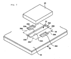
- FIG. 7 shows a semiconductor device packaging substrate 20 (referred to as the packaging substrate 20 hereinafter) as a first embodiment of the present invention.
- a semiconductor device (semiconductor element) 25 is mounted on this packaging substrate 20 by the flip-chip bonding.
- the semiconductor element 25 such as DRAM, having a center pad structure is mounted is shown.
- the packaging substrate 20 is a single-layer or multi-layer printed wiring board, and also predetermined wiring patterns, electrodes, etc. (not shown) made of copper, for example, are formed on its surface. Also, in order to protect the wiring patterns, the electrodes, etc., a solder resist 22 is provided on the surface to improve the soldering described later.
- the solder resist 22 is a resin that has insulating performance and also has a function of preventing adhesion of the solder.
- An opening portion 23 (a first opening portion) is formed in a portion, in which the electrodes to be bonded to the solder bumps formed on the semiconductor device 25 are formed, of a packaging area 26 of the solder resist 22, in which the semiconductor device 25 is mounted. Therefore, the electrodes bonded to the bumps formed on the packaging substrate 20 are exposed to the outside via the opening portion 23.
- the solder resist 22 is formed on the packaging substrate 20 by screen-printing method or photographic method.
- the photographic method is applied to form desired patterns by applying exposing/developing processes using ultraviolet rays, for example, after the solder resist 22 containing a photosensitizer is applied on the packaging substrate 20.
- the solder resist 22 can be formed easily by either of the screen-printing method and the photographic method.
- opening portions 30A as a second opening portion are formed on peripheral portions of the opening portion 23 in the solder resist 22. As described later, the opening portion 30A performs a function of adjusting a flow speed when providing underfill resin 27 (This opening portion 30A is referred to as the speed adjusting opening portion 30A hereinafter).
- a profile of the speed adjusting opening portion 30A is set like a rectangular shape when the packaging substrate 20 is viewed from the top. Also, arranging positions of the speed adjusting opening portions 30A are set in positions facing long sides of the opening portion 23, and partially cover (overlap with) outer peripheral portions 26A of a packaging area 26 for the semiconductor device 25.
- the speed adjusting opening portions 30A can be formed simultaneously when the opening portion 23 is formed in the solder resist 22 by the screen-printing method or the photographic method. Thus, such speed adjusting opening portions 30A can be formed easily, not making manufacturing steps complicated. Also, the profile of the speed adjusting opening portions 30A can be changed easily by changing a mask used in the screen-printing method or the photographic method. In particular, since the profile of the speed adjusting opening portions 30A is the rectangular shape as a simple shape in the present embodiment, the speed adjusting opening portions 30A can be formed simply.
- the semiconductor device 25 is flip-chip bonded to the packaging substrate 20 constructed as above.
- various bumps such as solder bumps and gold bumps (not shown in Fig. 7) are arranged on a bottom surface (circuit formed surface) of the semiconductor device 25, and then the semiconductor device 25 is mounted on the packaging substrate 20 by bonding the bumps to the electrodes formed on the packaging substrate 20 and exposed from the opening portion 23.
- FIG. 8 to FIG. 11 are plan views showing a flow of the underfill resin 27 when the underfill resin 27 is injected between the packaging substrate 20 and the semiconductor device 25.
- underfill resin 27 is provided between the packaging substrate 20 and the semiconductor device 25, illustration of the semiconductor device 25 is omitted herein and only its packaging area 26 is illustrated, for convenience of illustration.
- a liquid underfill resin 27 is injected in a space between the packaging substrate 20 and the semiconductor device 25 from an injection starting position 29.
- the injection starting position 29 is set in a position of the bottom portion of the opening portion 23.
- the underfill resin 27 when injected from the injection starting position 29 flows upward in FIG. 8 because of a capillarity (in the direction indicated with an arrow X in FIG. 8) to spread into a space between the packaging substrate 20 and the semiconductor device 25.
- a flow of the underfill resin 27 is not changed from the related art, as shown in FIG. 8, until such flow of the underfill resin 27 reaches the speed adjusting opening portion 30A. That is, a flow end surface 27A as a top end portion of the underfill resin 27 is not formed as a linear end but a curved end shown in FIG. 8.
- the underfill resin 27 that entered into the speed adjusting opening portion 30A flows such that the flow end surface 27A moves along the outer periphery of the speed adjusting opening portion 30A, a distance in which the underfill resin 27 flows (distance of the outer periphery) becomes longer. Also, since the underfill resin 27 flows in the speed adjusting opening portion 30A constructed as a recessed area, such underfill resin 27 does not go forward in the X direction to exceed the speed adjusting opening portion 30A until the speed adjusting opening portion 30A is filled with the underfill resin 27.
- the flow speed of the underfill resin 27 passing through the speed adjusting opening portion 30A can be made slow rather than the flow speed in other portions.
- the flow end surface 27A of the underfill resin 27 gives an almost uniform and smooth end, as shown in FIG. 9, at a point of time when the underfill resin 27 passes through the speed adjusting opening portion 30A.
- FIG. 10 shows a situation that the underfill resin 27 goes forward further in the X direction.
- the opening portion 23 is present in the center of the packaging area 26, the flow speed of the underfill resin 27 on the long side is increased by the edge portion 23A, while the flow speed of the underfill resin 27 on the outer peripheral portion 26A is decreased by the presence of the speed adjusting opening portion 30A. Therefore, as shown in FIG. 10, the underfill resin 27 goes forward in an egg-shaped end as a whole (the flow end surface 27A gives a curve whose center portion is protruded upwards).
- FIG. 11 shows a situation that a process of providing the underfill resin 27 is ended.
- a flow distribution of the underfill resin 27 gives such a distribution that the flow end surface 27A constitutes an almost uniform and smooth end.
- the underfill resin 27 flows in such a manner that a center portion goes ahead for some amount and both side portions follow the center portion slightly late.
- the underfill resin shows such a flow that the underfill resin goes around fast while leaving the center portion, and also it can be prevented that the voids are generated in the underfill resin 27.
- the packaging reliability in mounting the semiconductor device 25 on the packaging substrate 20 can be increased.
- the underfill resin 27 still remains in the speed adjusting opening portion 30A after the providing process is ended. Therefore, since the underfill resin 27 in the speed adjusting opening portion 30A has an anchor effect with respect to the packaging substrate 20, the underfill resin 27 can be secured to the packaging substrate 20 without fail. As a result, the packaging reliability in mounting the semiconductor device 25 on the packaging substrate 20 can be increased further.
- two speed adjusting opening portions 30A are provided to face the long sides of the opening portion 23, and the opening portion 23 is provided between them.
- a number of the speed adjusting opening portions 30A being arranged is not limited to two, and a plurality of speed adjusting opening portions may be employed.
- the arranging position is not limited to the positions shown in the present embodiment.
- the position may be selected appropriately to correspond to the flow of the underfill resin 27.
- the speed adjusting opening portion may be provided on the opposite side to the injection starting position 29 of the opening portion 23. With this configuration, it can be prevented that the underfill resin 27 flows out excessively from the packaging area 26 to the outside.
- the shape of the speed adjusting opening portion is not limited to the rectangular shape when viewed from the top.
- the speed adjusting opening portion may be in any shape as long as the underfill resin 27 is filled inside so as to prevent that the underfill resin goes around fast while leaving the center portion.
- FIG. 12 to FIG. 17 the same reference symbols are affixed to the same configurations as those shown in FIG. 7 to FIG. 11 used in the explanation in the first embodiment, and their explanation will be omitted herein.
- FIG. 12 shows the packaging substrate 20 as a second embodiment of the present invention.
- an example in which two opening portions 23, 24 are formed in the solder resist 22 to mount the semiconductor device having the pad structure in two rows is illustrated.
- the opening portions 23, 24 are arranged in parallel with each other, and the underfill resin 27 is injected in the direction that is perpendicular to the extending direction (the lateral direction in FIG. 12) of the opening portions 23, 24.
- the present embodiment is constructed such that the speed adjusting opening portion 30A is formed between the opening portion 23 and the opening portion 24.
- the speed adjusting opening portion 30A is formed between the opening portion 23 and the opening portion 24.
- FIG. 13 and FIG. 14 show the packaging substrates 20 as third and fourth embodiments of the present invention.
- the adjusting section for adjusting the flow speed of the underfill resin 27 is shaped into a polygonal shape when viewed from the top.
- FIG. 13 shows an example in which a cross-like shaped speed adjusting opening portion 30B is applied to the packaging substrate 20 having one opening portion 23.
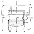
- FIG. 14 shows an example in which the cross-like shaped speed adjusting opening portion 30B is applied to the packaging substrate 20 having two opening portions 23, 24.
- the speed adjusting opening portion 30B is shaped into the polygonal shape, the flow speed of the underfill resin 27 can be reduced largely. Therefore, the flow speed of the underfill resin 27 can be decreased largely by a small space, and it can be prevented that a dead space is generated on the packaging substrate 20 when the speed adjusting opening portion 30B is provided.
- a cross-like shape is used as an example of a polygonal shape, but the polygonal shape is not limited to this shape.
- FIG. 15 to FIG. 17 show the packaging substrates 20 as fifth and sixth embodiments of the present invention.
- the flow speed of the underfill resin 27 is made slow by forming the opening portions 23, 24 in the solder resist 22 and forming the recess portion on the surface of the packaging substrate 20.
- speed adjusting convex portions 31 are formed on the solder resist 22 as the adjusting section to adjust the flow speed of the underfill resin 27.
- the speed adjusting convex portions 31 are convex portions that are formed integrally with the solder resist 22, as shown in FIG. 15, and are formed simultaneously when the solder resist 22 is formed. Concretely, the speed adjusting convex portions 31 are formed by providing the convex solder resist on the solder resist 22 by screen printing, or the like. Also, a height of the speed adjusting convex portions 31 is set almost equal to or slightly lower than a clearance between the semiconductor device 25 and the packaging substrate 20 when normally the semiconductor device 25 is flip-chip bonded to the packaging substrate 20.
- FIG. 15 and FIG. 16 show an example in which the speed adjusting convex portions 31 are applied to the packaging substrate 20 having one opening portion 23.
- FIG. 17 show an example in which the speed adjusting convex portions 31 are applied to the packaging substrate 20 having two opening portions 23, 24.
- the speed adjusting convex portions 31 since the speed adjusting convex portions 31 are formed on the solder resist 22, the speed adjusting convex portions 31 serve as a dam to prevent the flow of the underfill resin 27 when the underfill resin 27 comes up to the speed adjusting convex portions 31. Accordingly, the flow speed of the underfill resin 27 can be decreased, and also generation of the voids in the underfill resin 27 can be prevented.
Landscapes
- Encapsulation Of And Coatings For Semiconductor Or Solid State Devices (AREA)
- Wire Bonding (AREA)
- Structures Or Materials For Encapsulating Or Coating Semiconductor Devices Or Solid State Devices (AREA)
- Non-Metallic Protective Coatings For Printed Circuits (AREA)
- Electric Connection Of Electric Components To Printed Circuits (AREA)
Abstract
Description
- This application claims foreign priority based on
Japanese Patent application No. 2005-169894, filed June 9, 2005 - The present invention relates to a semiconductor device packaging substrate and a semiconductor device packaging structure, and more particularly, a semiconductor device packaging substrate and a semiconductor device packaging structure in which an underfill resin is filled between the packaging substrate and a semiconductor device mounted to the packaging substrate in flip-chip bonding.
- As a method of packaging a semiconductor device which is high in density onto a packaging substrate, flip-chip bonding is used frequently. According to this flip-chip bonding, the semiconductor device is mounted by providing solder bumps on the bottom surface of the semiconductor device as external connection terminals, then setting this semiconductor device in a face-down state to the packaging substrate, and then bonding the solder bumps to electrodes formed on the packaging substrate.
- FIG.1 shows an example of a
packaging substrate 1 on which a semiconductor device (semiconductor element) 5 is mounted by the flip-chip bonding in the related art. In FIG.1, an example in which thesemiconductor device 5, such as DRAM, having a center pad structure is mounted on thepackaging substrate 1 is shown. - The
packaging substrate 1 is a printed-wiring board, and predetermined wiring patterns, electrodes, etc. are formed on its surface. Also, a solder resist 2 for protecting the wiring patterns, the electrodes, etc. is provided on the surface of thepackaging substrate 1. - The
solder resist 2 is a resin that has insulating performance and also has a function of preventing adhesion of the solder. Anopening portion 3 is formed in a portion, in which the electrodes to be bonded to the solder bumps formed on thesemiconductor device 5 are formed, of apackaging area 6 of thesolder resist 2, in which thesemiconductor device 5 is mounted. Therefore, the electrodes (not shown) bonded to the bumps formed on thepackaging substrate 1 are exposed to the outside via theopening portion 3. - In the meanwhile, in a case where a difference in thermal expansion between the
packaging substrate 1 and thesemiconductor device 5 is large, a stress caused due to such difference in thermal expansion in heating is applied to the solder bumps when thesemiconductor device 5 is flip-chip bonded to thepackaging substrate 1. Thus, a problem arises in packaging reliability. Therefore, in the related art, a stress caused due to a difference in thermal expansion is suppressed by providing anunderfill resin 7 between thesemiconductor device 5 and thepackaging substrate 1 after thesemiconductor device 5 is flip-chip mounted on thepackaging substrate 1, and thus the packaging reliability is improved (seeJP-A-2002-329744 - FIG.2 is a plan view showing a process of providing the
underfill resin 7 between thepackaging substrate 1 and thesemiconductor device 5. Because theunderfill resin 7 is provided between thepackaging substrate 1 and thesemiconductor device 5, illustration of thesemiconductor device 5 is omitted herein and only itspackaging area 6 is illustrated, for convenience of illustration. - In order to provide the
underfill resin 7, aliquid underfill resin 7 is injected between thepackaging substrate 1 and thesemiconductor device 5 from aninjection starting position 9. In an example shown in FIG.2, theinjection starting position 9 is set in a position of the bottom portion of theopening portion 3 in FIG.2. The underfill resin 7 when injected from theinjection starting position 9 flows upward in FIG.2 to spread into a space between thepackaging substrate 1 and thesemiconductor device 5. - In this injection, a
flow end surface 7A as a top end portion of theunderfill resin 7 is not formed as a linear end but a curved end shown in FIG.2. This is caused due to the fact that a flow speed of the liquid underfill resin 7 in areas that are located alongedge portions 3A of theopening portion 3 and outerperipheral portions 6A of thesemiconductor device 5 is higher than that in other areas. More concretely, a flow speed V2 at theedge portion 3A and a flow speed V3 at the outerperipheral portion 6A is higher than a flow speed of theunderfill resin 7 on thesolder resist 2 indicated with an arrow V1 in FIG.2 (V1<V2, V1<V3). - Also, FIG.4 shows an example in which two
opening portions opening portions underfill resin 7 is injected in the direction that is perpendicular to theopening portions underfill resin 7 goes around fast conspicuously. - In this manner, a flow speed of the
underfill resin 7 is not uniform on thepackaging substrate 1, nevertheless this problem was not handled properly in the related art. For this reason, a curved shape of theflow end surface 7A becomes prominent based on a difference in speed when theunderfill resin 7 flows from theinjection starting position 9 to the opposite side. Then, because the portion of theunderfill resin 7 whose flow speed is fast flows to go around the portion whose flow speed is slow,voids 8 are generated in the inside of theunderfill resin 7 under certain circumstances, as shown in FIG.3 and FIG.5. - FIG. 6A shows an SAT (Scanning Acoustic Tomography) image in which
voids 8 are generated in the inside of theunderfill resin 7 when theunderfill resin 7 is injected between thepackaging substrate 1 and thesemiconductor device 5 as the first related art. FIG. 6B shows an image when surface grinding is performed in the state shown in FIG. 6A. - FIG. 6C is a cross-sectional view of a semiconductor device packaging structure along the line A-A' of FIG. 6A. In this case, an
Au stud bump 11 formed on thesemiconductor device 5 and a substrate conductor (electrode) 13 formed on thepackaging substrate 1 is connected via asolder 12. In FIG. 6C, voids are not generated. - FIG. 6D is a cross-sectional view of the semiconductor device packaging structure along the line B-B' of FIG. 6A. In this case, the
void 8 is generated in the inside of theunderfill resin 7 around thesolder 12 between thesemiconductor device 5 and thepackaging substrate 1. - FIG. 6E is a cross-sectional view of the semiconductor device packaging structure along the line C-C' of FIG. 6A. In this case, the
void 8 is generated in the inside of theunderfill resin 7 above thepackaging substrate 1 between thesemiconductor device 5 and thepackaging substrate 1. - In this manner, in case the
voids 8 are generated in the inside of theunderfill resin 7, it is possible that an air in thevoids 8 is expanded by the later heating resulting a breakage of theunderfill resin 7, or theunderfill resin 7 cannot sufficiently absorb a stress caused between thepackaging substrate 1 and thesemiconductor device 5. Thus, such a problem is caused that the packaging reliability is deteriorated. - The aforementioned problems are at least partly solved by a packaging substrate for a semiconductor device as laid out in
claim 1, a packaging structure as laid out inclaim 10, and a method as laid out inclaim 11. Further aspects, details, features and embodiments are evident from the dependent claims, the description and the accompanying drawings. - The present invention has been made in view of the above circumstances, and provides a semiconductor device packaging substrate and a semiconductor device packaging structure, capable of preventing generation of voids in an underfill resin.
- In some implementations, a packaging substrate of the invention for a semiconductor device comprises:
- a solder resist on a surface of the packaging substrate, the solder resist having a first opening portion for mounting the semiconductor device; and
- an adjusting section for adjusting a flow speed of an underfill resin when the underfill resin is provided, the adjusting section being positioned in vicinity of the first opening portion of the solder resist.
- Accordingly, since the adjusting section is provided in the peripheral portion of the first opening portion of the solder resist, the underfill resin moves over the adjusting section and is filled between the semiconductor device and the semiconductor device packaging substrate when providing the underfill resin. In this movement, since the adjusting section adjusts a flow speed of the underfill resin, the underfill resin can move uniformly and also generation of the voids in the underfill resin can be prevented.
- In the packaging substrate of an embodiment of the invention, the adjusting section includes a second opening portion formed in the solder resist.
- Accordingly, since the adjusting section is formed by the second opening portion formed in the solder resist, such adjusting section can be formed simultaneously with the first opening portion, and thus the adjusting section can be formed easily.
- In the packaging substrate of an embodiment of the invention, the adjusting section includes a convex portion formed on the solder resist.
- Accordingly, since the adjusting section is formed by the convex portion formed on the solder resist, such adjusting section can be formed simultaneously when the solder resist is formed, and thus the adjusting section can be formed easily.
- In the packaging substrate of an embodiment of the invention, the adjusting section is rectangular-shaped when viewed from a top.
- Accordingly, since the adjusting section is shaped into a rectangular shape as a simple shape, the formation of the adjusting section can be executed simply.
- In the packaging substrate of an embodiment of the invention, the adjusting section is polygonal-shaped when viewed from a top.
- Accordingly, since the adjusting section is shaped into a polygonal shape, a flow speed of the underfill resin can be decreased largely with a small space.
- In the packaging substrate of an embodiment of the invention, the adjusting section is provided on one side of the first opening portion, the side that is opposite to an injection starting position of the underfill resin.
- Accordingly, it can be prevented that the underfill resin flows out excessively from the opposite side of the first opening portion.
- In the packaging substrate of an embodiment of the invention, the adjusting section is formed in a position partially covering an outer periphery of a region in which the semiconductor device is mounted.
- Accordingly, since the adjusting section is provided in the outer periphery, in which a flow speed of the underfill resin is fast, of the region, the underfill resin can be provided in further uniform state.
- In some implementations, a packaging structure of the invention comprises:
- a packaging substrate;
- a semiconductor device mounted in the packaging substrate in flip-chip bonding; and
- an underfill resin provided between the semiconductor device and the packaging substrate,
- wherein the packaging substrate includes:
- a solder resist on a surface of the packaging substrate, the solder resist having a first opening portion for mounting the semiconductor device; and
- an adjusting section for adjusting a flow speed of the underfill resin when the underfill resin is provided, the adjusting section being positioned in vicinity of the first opening portion of the solder resist, and
- the underfill resin is provided in a region including the first opening portion and the adjusting section.
- Accordingly, since the underfill resin moves over the adjusting section when providing the underfill resin, the flow speed is adjusted and therefore generation of the voids in the underfill resin can be prevented. Also, since the underfill resin is provided in the region including the adjusting section, after the underfill resin is provided, the underfill resin can be secured without fail on the semiconductor device packaging substrate by an anchor effect of the adjusting section.
- Accordingly, since the adjusting section adjusts the flow speed of the underfill resin, the underfill resin can move uniformly, and also generation of the voids in the underfill resin can be prevented.
- The invention is also directed to an apparatus for carrying out the disclosed methods and including apparatus parts for performing each described method steps. These method steps may be performed by way of hardware components, a computer programmed by appropriate software, by any combination of the two or in any other manner. Furthermore, the invention is also directed to methods by which the described apparatus operates. It includes method steps for carrying out every function of the apparatus.
- The accompanying drawings relate to embodiments of the invention and are described in the following:
- FIG.1 is a perspective view showing a first related art of a packaging substrate.
- FIG.2 is a view explaining a flow of an underfill resin in the packaging substrate according to the first related art.
- FIG.3 is a view explaining a problem that is caused in the packaging substrate according to the first related art.
- FIG.4 is a view explaining a flow of the underfill resin in a packaging substrate according to a second related art.
- FIG.5 is a view explaining a problem that is caused in the packaging substrate according to the second related art.
- FIG. 6A shows an SAT image in which voids are generated in the inside of an underfill resin when the underfill resin is injected between the packaging substrate and the semiconductor device as the first related art.
- FIG. 6B shows an image when surface grinding is performed in the state shown in FIG. 6A.
- FIG. 6C is a cross-sectional view of a semiconductor device packaging structure along the line A-A' of FIG. 6A.
- FIG. 6D is a cross-sectional view of the semiconductor device packaging structure along the line B-B' of FIG. 6A.
- FIG. 6E is a cross-sectional view of the semiconductor device packaging structure along the line C-C' of FIG. 6A.
- FIG. 7 is a perspective view showing a packaging substrate as a first embodiment of the present invention.
- FIG. 8 is a view (#1) explaining a flow of the underfill resin in the packaging substrate as a first embodiment of the present invention.
- FIG. 9 is a view (#2) explaining a flow of the underfill resin in the packaging substrate as a first embodiment of the present invention.
- FIG. 10 is a view (#3) explaining a flow of the underfill resin in the packaging substrate as a first embodiment of the present invention.
- FIG. 11 is a view (#4) explaining a flow of the underfill resin in the packaging substrate as a first embodiment of the present invention.
- FIG. 12 is a plan view of a packaging substrate as a second embodiment of the present invention.
- FIG. 13 is a plan view of a packaging substrate as a third embodiment of the present invention.
- FIG. 14 is a plan view of a packaging substrate as a fourth embodiment of the present invention.
- FIG. 15 is a perspective view of a packaging substrate as a fifth embodiment of the present invention.
- FIG. 16 is a plan view of the packaging substrate as the fifth embodiment of the present invention.
- FIG. 17 is a plan view of a packaging substrate as a sixth embodiment of the present invention.
- Next, a best mode for carrying out the present invention will be explained with reference to the drawings hereinafter.
- FIG. 7 shows a semiconductor device packaging substrate 20 (referred to as the
packaging substrate 20 hereinafter) as a first embodiment of the present invention. A semiconductor device (semiconductor element) 25 is mounted on thispackaging substrate 20 by the flip-chip bonding. In FIG. 7, an example in which thesemiconductor element 25, such as DRAM, having a center pad structure is mounted is shown. - The
packaging substrate 20 is a single-layer or multi-layer printed wiring board, and also predetermined wiring patterns, electrodes, etc. (not shown) made of copper, for example, are formed on its surface. Also, in order to protect the wiring patterns, the electrodes, etc., a solder resist 22 is provided on the surface to improve the soldering described later. - The solder resist 22 is a resin that has insulating performance and also has a function of preventing adhesion of the solder. An opening portion 23 (a first opening portion) is formed in a portion, in which the electrodes to be bonded to the solder bumps formed on the
semiconductor device 25 are formed, of apackaging area 26 of the solder resist 22, in which thesemiconductor device 25 is mounted. Therefore, the electrodes bonded to the bumps formed on thepackaging substrate 20 are exposed to the outside via the openingportion 23. - The solder resist 22 is formed on the
packaging substrate 20 by screen-printing method or photographic method. Here, the photographic method is applied to form desired patterns by applying exposing/developing processes using ultraviolet rays, for example, after the solder resist 22 containing a photosensitizer is applied on thepackaging substrate 20. The solder resist 22 can be formed easily by either of the screen-printing method and the photographic method. - Also, in the present embodiment, opening
portions 30A as a second opening portion are formed on peripheral portions of the openingportion 23 in the solder resist 22. As described later, theopening portion 30A performs a function of adjusting a flow speed when providing underfill resin 27 (Thisopening portion 30A is referred to as the speed adjustingopening portion 30A hereinafter). - In the present embodiment, a profile of the speed adjusting
opening portion 30A is set like a rectangular shape when thepackaging substrate 20 is viewed from the top. Also, arranging positions of the speed adjustingopening portions 30A are set in positions facing long sides of the openingportion 23, and partially cover (overlap with) outerperipheral portions 26A of apackaging area 26 for thesemiconductor device 25. - The speed adjusting
opening portions 30A can be formed simultaneously when the openingportion 23 is formed in the solder resist 22 by the screen-printing method or the photographic method. Thus, such speed adjustingopening portions 30A can be formed easily, not making manufacturing steps complicated. Also, the profile of the speed adjustingopening portions 30A can be changed easily by changing a mask used in the screen-printing method or the photographic method. In particular, since the profile of the speed adjustingopening portions 30A is the rectangular shape as a simple shape in the present embodiment, the speed adjustingopening portions 30A can be formed simply. - The
semiconductor device 25 is flip-chip bonded to thepackaging substrate 20 constructed as above. In other words, various bumps such as solder bumps and gold bumps (not shown in Fig. 7) are arranged on a bottom surface (circuit formed surface) of thesemiconductor device 25, and then thesemiconductor device 25 is mounted on thepackaging substrate 20 by bonding the bumps to the electrodes formed on thepackaging substrate 20 and exposed from the openingportion 23. - In the meanwhile, in the case where a difference in thermal expansion between the
packaging substrate 20 and thesemiconductor device 25 is large, a stress caused due to such difference in thermal expansion in heating is applied to the bumps when thesemiconductor device 25 is flip-chip bonded to thepackaging substrate 20. Thus, as described above, a problem arises in packaging reliability. Therefore, in the present embodiment, a stress caused due to a difference in thermal expansion is suppressed by providing theunderfill resin 27 between thesemiconductor device 25 and thepackaging substrate 20 after thesemiconductor device 25 is flip-chip mounted on thepackaging substrate 20, and thus improvement of the packaging reliability can be achieved. - Then, a process of providing the
underfill resin 27 when thepackaging substrate 20 according to the present embodiment is employed will be explained hereunder. FIG. 8 to FIG. 11 are plan views showing a flow of theunderfill resin 27 when theunderfill resin 27 is injected between thepackaging substrate 20 and thesemiconductor device 25. - Here, because the
underfill resin 27 is provided between thepackaging substrate 20 and thesemiconductor device 25, illustration of thesemiconductor device 25 is omitted herein and only itspackaging area 26 is illustrated, for convenience of illustration. - In order to provide the
underfill resin 27, aliquid underfill resin 27 is injected in a space between thepackaging substrate 20 and thesemiconductor device 25 from aninjection starting position 29. In an example shown in FIG. 8, theinjection starting position 29 is set in a position of the bottom portion of the openingportion 23. Theunderfill resin 27 when injected from theinjection starting position 29 flows upward in FIG. 8 because of a capillarity (in the direction indicated with an arrow X in FIG. 8) to spread into a space between thepackaging substrate 20 and thesemiconductor device 25. - In this injection, a flow of the
underfill resin 27 is not changed from the related art, as shown in FIG. 8, until such flow of theunderfill resin 27 reaches the speed adjustingopening portion 30A. That is, aflow end surface 27A as a top end portion of theunderfill resin 27 is not formed as a linear end but a curved end shown in FIG. 8. - As described above, this is caused due to the fact that a flow speed of the
liquid underfill resin 27 in areas that are located alongedge portions 23A of the openingportion 23 and outerperipheral portions 26A of thesemiconductor device 25 is higher than that in other areas. Therefore, a flow speed V2 at theedge portion 23A and a flow speed V3 at the outerperipheral portion 26A is higher than a flow speed of theunderfill resin 27 on the solder resist 22 indicated with an arrow V1 in FIG. 8 (V1<V2, V1<V3). - When the
underfill resin 27 goes past the position shown in FIG. 8 and reaches the speed adjustingopening portion 30A,such underfill resin 27 enters into the speed adjustingopening portion 30A. At this time, in the present embodiment, because the speed adjustingopening portion 30A is formed in the position containing the outerperipheral portion 26A in which the flow speed of theunderfill resin 27 is fast, theunderfill resin 27 having the fast flow speed flows into the speed adjustingopening portion 30A. - Since the
underfill resin 27 that entered into the speed adjustingopening portion 30A flows such that theflow end surface 27A moves along the outer periphery of the speed adjustingopening portion 30A, a distance in which theunderfill resin 27 flows (distance of the outer periphery) becomes longer. Also, since theunderfill resin 27 flows in the speed adjustingopening portion 30A constructed as a recessed area,such underfill resin 27 does not go forward in the X direction to exceed the speed adjustingopening portion 30A until the speed adjustingopening portion 30A is filled with theunderfill resin 27. - In other words, because the speed adjusting
opening portion 30A is formed, the flow speed of theunderfill resin 27 passing through the speed adjustingopening portion 30A can be made slow rather than the flow speed in other portions. In this manner, since the flow speed of theunderfill resin 27 is adjusted by the speed adjustingopening portion 30A, theflow end surface 27A of theunderfill resin 27 gives an almost uniform and smooth end, as shown in FIG. 9, at a point of time when theunderfill resin 27 passes through the speed adjustingopening portion 30A. - FIG. 10 shows a situation that the
underfill resin 27 goes forward further in the X direction. As shown in FIG. 10, because the openingportion 23 is present in the center of thepackaging area 26, the flow speed of theunderfill resin 27 on the long side is increased by theedge portion 23A, while the flow speed of theunderfill resin 27 on the outerperipheral portion 26A is decreased by the presence of the speed adjustingopening portion 30A. Therefore, as shown in FIG. 10, theunderfill resin 27 goes forward in an egg-shaped end as a whole (theflow end surface 27A gives a curve whose center portion is protruded upwards). - FIG. 11 shows a situation that a process of providing the
underfill resin 27 is ended. As shown in FIG. 10, in the present embodiment, because the speed adjustingopening portion 30A is provided in thepackaging substrate 20, a flow distribution of theunderfill resin 27 gives such a distribution that theflow end surface 27A constitutes an almost uniform and smooth end. - More concretely, as shown in FIG. 10, the
underfill resin 27 flows in such a manner that a center portion goes ahead for some amount and both side portions follow the center portion slightly late. As a result, unlike the related art, it can be prevented that the underfill resin shows such a flow that the underfill resin goes around fast while leaving the center portion, and also it can be prevented that the voids are generated in theunderfill resin 27. In this manner, since generation of the voids in theunderfill resin 27 can be suppressed, the packaging reliability in mounting thesemiconductor device 25 on thepackaging substrate 20 can be increased. - In addition, the
underfill resin 27 still remains in the speed adjustingopening portion 30A after the providing process is ended. Therefore, since theunderfill resin 27 in the speed adjustingopening portion 30A has an anchor effect with respect to thepackaging substrate 20, theunderfill resin 27 can be secured to thepackaging substrate 20 without fail. As a result, the packaging reliability in mounting thesemiconductor device 25 on thepackaging substrate 20 can be increased further. - In the present embodiment, two speed adjusting
opening portions 30A are provided to face the long sides of the openingportion 23, and the openingportion 23 is provided between them. But a number of the speed adjustingopening portions 30A being arranged is not limited to two, and a plurality of speed adjusting opening portions may be employed. - Also, the arranging position is not limited to the positions shown in the present embodiment. The position may be selected appropriately to correspond to the flow of the
underfill resin 27. For example, the speed adjusting opening portion may be provided on the opposite side to theinjection starting position 29 of the openingportion 23. With this configuration, it can be prevented that theunderfill resin 27 flows out excessively from thepackaging area 26 to the outside. - Furthermore, the shape of the speed adjusting opening portion is not limited to the rectangular shape when viewed from the top. The speed adjusting opening portion may be in any shape as long as the
underfill resin 27 is filled inside so as to prevent that the underfill resin goes around fast while leaving the center portion. - Next, second to sixth embodiments of the present invention will be explained with FIG. 12 to FIG. 17 hereunder. In FIG. 12 to FIG. 17, the same reference symbols are affixed to the same configurations as those shown in FIG. 7 to FIG. 11 used in the explanation in the first embodiment, and their explanation will be omitted herein.
- FIG. 12 shows the
packaging substrate 20 as a second embodiment of the present invention. In the present embodiment, an example in which two openingportions portions underfill resin 27 is injected in the direction that is perpendicular to the extending direction (the lateral direction in FIG. 12) of the openingportions - Also, the present embodiment is constructed such that the speed adjusting
opening portion 30A is formed between the openingportion 23 and the openingportion 24. As in the present embodiment, even in the configuration that two openingportions underfill resin 27 and theunderfill resin 27 is subject to go around along edges, the going-around of theunderfill resin 27 can be suppressed and also generation of the voids can be prevented since the flow speed of theunderfill resin 27 is adjusted by the speed adjustingopening portion 30A. - FIG. 13 and FIG. 14 show the
packaging substrates 20 as third and fourth embodiments of the present invention. In thepackaging substrates 20 according to the third and fourth embodiments, the adjusting section for adjusting the flow speed of theunderfill resin 27 is shaped into a polygonal shape when viewed from the top. FIG. 13 shows an example in which a cross-like shaped speed adjustingopening portion 30B is applied to thepackaging substrate 20 having one openingportion 23. Also, FIG. 14 shows an example in which the cross-like shaped speed adjustingopening portion 30B is applied to thepackaging substrate 20 having two openingportions - In this manner, because the speed adjusting
opening portion 30B is shaped into the polygonal shape, the flow speed of theunderfill resin 27 can be reduced largely. Therefore, the flow speed of theunderfill resin 27 can be decreased largely by a small space, and it can be prevented that a dead space is generated on thepackaging substrate 20 when the speed adjustingopening portion 30B is provided. - Accordingly, improvement of the packaging reliability can be achieved while attaining a size reduction of the
packaging substrate 20. In the present embodiment, a cross-like shape is used as an example of a polygonal shape, but the polygonal shape is not limited to this shape. - FIG. 15 to FIG. 17 show the
packaging substrates 20 as fifth and sixth embodiments of the present invention. - In the above embodiments, the flow speed of the
underfill resin 27 is made slow by forming the openingportions packaging substrate 20. In contrast, in thepackaging substrates 20 as the fifth and sixth embodiments, speed adjustingconvex portions 31 are formed on the solder resist 22 as the adjusting section to adjust the flow speed of theunderfill resin 27. - The speed adjusting
convex portions 31 are convex portions that are formed integrally with the solder resist 22, as shown in FIG. 15, and are formed simultaneously when the solder resist 22 is formed. Concretely, the speed adjustingconvex portions 31 are formed by providing the convex solder resist on the solder resist 22 by screen printing, or the like. Also, a height of the speed adjustingconvex portions 31 is set almost equal to or slightly lower than a clearance between thesemiconductor device 25 and thepackaging substrate 20 when normally thesemiconductor device 25 is flip-chip bonded to thepackaging substrate 20. - FIG. 15 and FIG. 16 show an example in which the speed adjusting
convex portions 31 are applied to thepackaging substrate 20 having one openingportion 23. Also, FIG. 17 show an example in which the speed adjustingconvex portions 31 are applied to thepackaging substrate 20 having two openingportions convex portions 31 are formed on the solder resist 22, the speed adjustingconvex portions 31 serve as a dam to prevent the flow of theunderfill resin 27 when theunderfill resin 27 comes up to the speed adjustingconvex portions 31. Accordingly, the flow speed of theunderfill resin 27 can be decreased, and also generation of the voids in theunderfill resin 27 can be prevented. - Also, as shown FIG. 15 and FIG. 16, since the speed adjusting
convex portions 31 are formed at corner portions on the opposite side to theinjection starting position 29 of thepackaging area 26, it can be prevented that theunderfill resin 27 flows out unnecessarily to the outside from thepackaging area 26. - It will be apparent to those skilled in the art that various modifications and variations can be made to the described preferred embodiments of the present invention without departing from the spirit or scope of the invention. Thus, it is intended that the present invention cover all modifications and variations of this invention consistent with the scope of the appended claims and their equivalents.
Claims (11)
- A packaging substrate for a semiconductor device, the packaging substrate comprising:a solder resist on a surface of the packaging substrate, the solder resist having a first opening portion for mounting the semiconductor device; andan adjusting section for adjusting a flow speed of an underfill resin when the underfill resin is provided, the adjusting section being positioned in vicinity of the first opening portion of the solder resist.
- The packaging substrate according to claim 1, wherein the adjusting section includes a second opening portion formed in the solder resist.
- The packaging substrate according to claim 1, wherein the adjusting section includes a convex portion formed on the solder resist.
- The packaging substrate according to claim 2, wherein the adjusting section is rectangular-shaped when viewed from a top.
- The packaging substrate according to claim 3, wherein the adjusting section is rectangular-shaped when viewed from a top.
- The packaging substrate according to claim 2, wherein the adjusting section is polygonal-shaped when viewed from a top.
- The packaging substrate according to claim 3, wherein the adjusting section is polygonal-shaped when viewed from a top.
- The packaging substrate according to claim 1, wherein the adjusting section is provided on one side of the first opening portion, the side that is opposite to an injection starting position of the underfill resin.
- The packaging substrate according to claim 1, wherein the adjusting section is formed in a position partially covering an outer periphery of a region in which the semiconductor device is mounted.
- A packaging structure comprising:a packaging substrate;a semiconductor device mounted in the packaging substrate in flip-chip bonding; andan underfill resin provided between the semiconductor device and the packaging substrate,wherein the packaging substrate includes:a solder resist on a surface of the packaging substrate, the solder resist having a first opening portion for mounting the semiconductor device; andan adjusting section for adjusting a flow speed of the underfill resin when the underfill resin is provided, the adjusting section being positioned in vicinity of the first opening portion of the solder resist, andthe underfill resin is provided in a region including the first opening portion and the adjusting section.
- A method for manufacturing a packaging substrate for a semiconductor device, comprising the steps of:a) providing a solder resist on a surface of the packaging substrate, the solder resist having a first opening for mounting the semiconductor device;b) positioning an adjusting section for adjusting a flow speed of an underfill resin when the underfill resin is provided in the vicinity of the first opening portion of the solder resist.
Applications Claiming Priority (1)
| Application Number | Priority Date | Filing Date | Title |
|---|---|---|---|
| JP2005169894A JP4536603B2 (en) | 2005-06-09 | 2005-06-09 | Manufacturing method of semiconductor device, mounting substrate for semiconductor device, and semiconductor device |
Publications (2)
| Publication Number | Publication Date |
|---|---|
| EP1732117A2 true EP1732117A2 (en) | 2006-12-13 |
| EP1732117A3 EP1732117A3 (en) | 2010-03-31 |
Family
ID=36942285
Family Applications (1)
| Application Number | Title | Priority Date | Filing Date |
|---|---|---|---|
| EP06011898A Withdrawn EP1732117A3 (en) | 2005-06-09 | 2006-06-09 | Semiconductor device packaging substrate and semiconductor device packaging structure |
Country Status (6)
| Country | Link |
|---|---|
| US (1) | US7375433B2 (en) |
| EP (1) | EP1732117A3 (en) |
| JP (1) | JP4536603B2 (en) |
| KR (1) | KR101212661B1 (en) |
| CN (1) | CN100521184C (en) |
| TW (1) | TWI390685B (en) |
Cited By (1)
| Publication number | Priority date | Publication date | Assignee | Title |
|---|---|---|---|---|
| WO2013036395A1 (en) * | 2011-09-10 | 2013-03-14 | Ati Technologies Ulc | Solder mask with anchor structures |
Families Citing this family (17)
| Publication number | Priority date | Publication date | Assignee | Title |
|---|---|---|---|---|
| US8106521B2 (en) * | 2006-10-19 | 2012-01-31 | Panasonic Corporation | Semiconductor device mounted structure with an underfill sealing-bonding resin with voids |
| JP5331303B2 (en) * | 2006-11-09 | 2013-10-30 | ルネサスエレクトロニクス株式会社 | Manufacturing method of semiconductor device |
| DE102007044620A1 (en) * | 2007-09-19 | 2009-04-16 | Semikron Elektronik Gmbh & Co. Kg | Arrangement with a connection device and at least one semiconductor component |
| JP5446867B2 (en) * | 2007-10-10 | 2014-03-19 | 日本電気株式会社 | Semiconductor device |
| JP4971243B2 (en) * | 2008-05-15 | 2012-07-11 | 新光電気工業株式会社 | Wiring board |
| JP5280139B2 (en) * | 2008-09-19 | 2013-09-04 | ルネサスエレクトロニクス株式会社 | Semiconductor device manufacturing method and mounting substrate |
| JP5117371B2 (en) * | 2008-12-24 | 2013-01-16 | 新光電気工業株式会社 | Semiconductor device and manufacturing method thereof |
| JP5472726B2 (en) * | 2009-02-24 | 2014-04-16 | 日立化成株式会社 | Wiring board, electronic component package and manufacturing method thereof |
| KR101630394B1 (en) * | 2010-03-08 | 2016-06-24 | 삼성전자주식회사 | Package substrate, semiconductor package comprising the same and method for fabricating the semiconductor package |
| WO2012060034A1 (en) * | 2010-11-04 | 2012-05-10 | アルプス電気株式会社 | Electronic component module |
| KR101197846B1 (en) | 2010-11-30 | 2012-11-05 | 삼성전기주식회사 | An array for manufacturing a printed circuit board and method of manufacturing flip chip on printed circuit board by using the same |
| KR101388739B1 (en) * | 2012-04-27 | 2014-04-25 | 삼성전기주식회사 | Semiconductor package |
| JP5954075B2 (en) * | 2012-09-21 | 2016-07-20 | ソニー株式会社 | Semiconductor device and manufacturing method of semiconductor device |
| JP2019029459A (en) * | 2017-07-27 | 2019-02-21 | 豊田合成株式会社 | Light emitting device and manufacturing method thereof |
| US11282717B2 (en) * | 2018-03-30 | 2022-03-22 | Intel Corporation | Micro-electronic package with substrate protrusion to facilitate dispense of underfill between a narrow die-to-die gap |
| JP7021625B2 (en) * | 2018-09-28 | 2022-02-17 | 豊田合成株式会社 | Luminescent device |
| JP7178978B2 (en) * | 2019-10-24 | 2022-11-28 | 三菱電機株式会社 | Semiconductor device and method for manufacturing semiconductor device |
Citations (4)
| Publication number | Priority date | Publication date | Assignee | Title |
|---|---|---|---|---|
| US5647123A (en) | 1995-10-16 | 1997-07-15 | Motorola, Inc. | Method for improving distribution of underfill between a flip chip die and a circuit board |
| JPH11284032A (en) | 1998-03-26 | 1999-10-15 | Ricoh Co Ltd | Flip chip connection method and flip chip connection structure |
| US6011312A (en) | 1996-07-30 | 2000-01-04 | Kabushiki Kaisha Toshiba | Flip-chip semiconductor package |
| US6094354A (en) | 1996-12-03 | 2000-07-25 | Nec Corporation | Chip component mounting board, chip component mounting structure, and method of manufacturing chip component mounting board |
Family Cites Families (4)
| Publication number | Priority date | Publication date | Assignee | Title |
|---|---|---|---|---|
| JP2571024B2 (en) * | 1994-09-28 | 1997-01-16 | 日本電気株式会社 | Multi-chip module |
| JP3581111B2 (en) | 2001-05-01 | 2004-10-27 | 新光電気工業株式会社 | Semiconductor device mounting substrate and mounting structure |
| US6815831B2 (en) * | 2001-12-12 | 2004-11-09 | Intel Corporation | Flip-chip device with multi-layered underfill having graded coefficient of thermal expansion |
| JP3964911B2 (en) * | 2004-09-03 | 2007-08-22 | 松下電器産業株式会社 | Manufacturing method of substrate with bumps |
-
2005
- 2005-06-09 JP JP2005169894A patent/JP4536603B2/en not_active Expired - Fee Related
-
2006
- 2006-06-07 KR KR1020060050913A patent/KR101212661B1/en not_active Expired - Fee Related
- 2006-06-08 US US11/423,056 patent/US7375433B2/en not_active Expired - Fee Related
- 2006-06-09 EP EP06011898A patent/EP1732117A3/en not_active Withdrawn
- 2006-06-09 CN CNB2006100828027A patent/CN100521184C/en not_active Expired - Fee Related
- 2006-06-09 TW TW095120623A patent/TWI390685B/en not_active IP Right Cessation
Patent Citations (4)
| Publication number | Priority date | Publication date | Assignee | Title |
|---|---|---|---|---|
| US5647123A (en) | 1995-10-16 | 1997-07-15 | Motorola, Inc. | Method for improving distribution of underfill between a flip chip die and a circuit board |
| US6011312A (en) | 1996-07-30 | 2000-01-04 | Kabushiki Kaisha Toshiba | Flip-chip semiconductor package |
| US6094354A (en) | 1996-12-03 | 2000-07-25 | Nec Corporation | Chip component mounting board, chip component mounting structure, and method of manufacturing chip component mounting board |
| JPH11284032A (en) | 1998-03-26 | 1999-10-15 | Ricoh Co Ltd | Flip chip connection method and flip chip connection structure |
Cited By (2)
| Publication number | Priority date | Publication date | Assignee | Title |
|---|---|---|---|---|
| WO2013036395A1 (en) * | 2011-09-10 | 2013-03-14 | Ati Technologies Ulc | Solder mask with anchor structures |
| US8772083B2 (en) | 2011-09-10 | 2014-07-08 | Ati Technologies Ulc | Solder mask with anchor structures |
Also Published As
| Publication number | Publication date |
|---|---|
| JP2006344822A (en) | 2006-12-21 |
| US7375433B2 (en) | 2008-05-20 |
| JP4536603B2 (en) | 2010-09-01 |
| TWI390685B (en) | 2013-03-21 |
| KR20060128681A (en) | 2006-12-14 |
| EP1732117A3 (en) | 2010-03-31 |
| TW200709379A (en) | 2007-03-01 |
| KR101212661B1 (en) | 2012-12-14 |
| CN1945820A (en) | 2007-04-11 |
| US20060281220A1 (en) | 2006-12-14 |
| CN100521184C (en) | 2009-07-29 |
Similar Documents
| Publication | Publication Date | Title |
|---|---|---|
| US7375433B2 (en) | Semiconductor device packaging substrate and semiconductor device packaging structure | |
| JP4438006B2 (en) | Semiconductor device and manufacturing method of semiconductor device | |
| US7911050B2 (en) | Semiconductor device and method for manufacturing the same | |
| CN100508177C (en) | Semiconductor device | |
| US6734557B2 (en) | Semiconductor device | |
| KR101578175B1 (en) | Wiring board and semiconductor device | |
| US7102239B2 (en) | Chip carrier for semiconductor chip | |
| US20050103516A1 (en) | Flip-chip mounting circuit board, manufacturing method thereof and integrated circuit device | |
| US7049687B2 (en) | Tape carrier package having stacked semiconductor elements, and short and long leads | |
| WO2011102100A1 (en) | Semiconductor device and stacked-type semiconductor device | |
| US5707714A (en) | Printed circuit board for flow soldering | |
| JP2004349399A (en) | Component mounting board | |
| KR20160022603A (en) | Flip chip package and method for manufacturing thereof | |
| KR20130122218A (en) | Method for manufacturing underfill flip chip package | |
| JP2009188275A (en) | Semiconductor chip, semiconductor device, semiconductor device manufacturing method, and liquid crystal module | |
| JP3147162B2 (en) | Bump arrangement method for flip chip integrated circuit and flip chip integrated circuit | |
| JP2010205946A (en) | Printed wiring board | |
| JP2005209991A (en) | Semiconductor device | |
| JP2007234988A (en) | Semiconductor element mounting substrate and mounting method | |
| KR20160140174A (en) | Electrical apparatus having electrical pattern capable of preventing solder bridge | |
| JP2004319692A (en) | Electronic circuit board | |
| US20250336857A1 (en) | Semiconductor Package | |
| JP2001267452A (en) | Semiconductor device | |
| JP4577686B2 (en) | Semiconductor device and manufacturing method thereof | |
| JP2001358253A (en) | BGA type semiconductor device |
Legal Events
| Date | Code | Title | Description |
|---|---|---|---|
| PUAI | Public reference made under article 153(3) epc to a published international application that has entered the european phase |
Free format text: ORIGINAL CODE: 0009012 |
|
| AK | Designated contracting states |
Kind code of ref document: A2 Designated state(s): AT BE BG CH CY CZ DE DK EE ES FI FR GB GR HU IE IS IT LI LT LU LV MC NL PL PT RO SE SI SK TR |
|
| AX | Request for extension of the european patent |
Extension state: AL BA HR MK YU |
|
| PUAL | Search report despatched |
Free format text: ORIGINAL CODE: 0009013 |
|
| AK | Designated contracting states |
Kind code of ref document: A3 Designated state(s): AT BE BG CH CY CZ DE DK EE ES FI FR GB GR HU IE IS IT LI LT LU LV MC NL PL PT RO SE SI SK TR |
|
| AX | Request for extension of the european patent |
Extension state: AL BA HR MK RS |
|
| 17P | Request for examination filed |
Effective date: 20100922 |
|
| AKX | Designation fees paid |
Designated state(s): DE FI FR NL |
|
| 17Q | First examination report despatched |
Effective date: 20110311 |
|
| STAA | Information on the status of an ep patent application or granted ep patent |
Free format text: STATUS: THE APPLICATION HAS BEEN WITHDRAWN |
|
| 18W | Application withdrawn |
Effective date: 20150415 |