EP1729348A2 - Junction box for a solar cell modul - Google Patents
Junction box for a solar cell modul Download PDFInfo
- Publication number
- EP1729348A2 EP1729348A2 EP06010045A EP06010045A EP1729348A2 EP 1729348 A2 EP1729348 A2 EP 1729348A2 EP 06010045 A EP06010045 A EP 06010045A EP 06010045 A EP06010045 A EP 06010045A EP 1729348 A2 EP1729348 A2 EP 1729348A2
- Authority
- EP
- European Patent Office
- Prior art keywords
- clamping
- connection
- conductor
- clamping device
- solar cell
- Prior art date
- Legal status (The legal status is an assumption and is not a legal conclusion. Google has not performed a legal analysis and makes no representation as to the accuracy of the status listed.)
- Granted
Links
Images

Classifications
-
- H—ELECTRICITY
- H02—GENERATION; CONVERSION OR DISTRIBUTION OF ELECTRIC POWER
- H02S—GENERATION OF ELECTRIC POWER BY CONVERSION OF INFRARED RADIATION, VISIBLE LIGHT OR ULTRAVIOLET LIGHT, e.g. USING PHOTOVOLTAIC [PV] MODULES
- H02S40/00—Components or accessories in combination with PV modules, not provided for in groups H02S10/00 - H02S30/00
- H02S40/30—Electrical components
- H02S40/34—Electrical components comprising specially adapted electrical connection means to be structurally associated with the PV module, e.g. junction boxes
-
- H—ELECTRICITY
- H01—ELECTRIC ELEMENTS
- H01R—ELECTRICALLY-CONDUCTIVE CONNECTIONS; STRUCTURAL ASSOCIATIONS OF A PLURALITY OF MUTUALLY-INSULATED ELECTRICAL CONNECTING ELEMENTS; COUPLING DEVICES; CURRENT COLLECTORS
- H01R4/00—Electrically-conductive connections between two or more conductive members in direct contact, i.e. touching one another; Means for effecting or maintaining such contact; Electrically-conductive connections having two or more spaced connecting locations for conductors and using contact members penetrating insulation
- H01R4/28—Clamped connections, spring connections
- H01R4/48—Clamped connections, spring connections utilising a spring, clip, or other resilient member
- H01R4/4809—Clamped connections, spring connections utilising a spring, clip, or other resilient member using a leaf spring to bias the conductor toward the busbar
- H01R4/48185—Clamped connections, spring connections utilising a spring, clip, or other resilient member using a leaf spring to bias the conductor toward the busbar adapted for axial insertion of a wire end
- H01R4/4819—Clamped connections, spring connections utilising a spring, clip, or other resilient member using a leaf spring to bias the conductor toward the busbar adapted for axial insertion of a wire end the spring shape allowing insertion of the conductor end when the spring is unbiased
- H01R4/4821—Single-blade spring
-
- H—ELECTRICITY
- H01—ELECTRIC ELEMENTS
- H01R—ELECTRICALLY-CONDUCTIVE CONNECTIONS; STRUCTURAL ASSOCIATIONS OF A PLURALITY OF MUTUALLY-INSULATED ELECTRICAL CONNECTING ELEMENTS; COUPLING DEVICES; CURRENT COLLECTORS
- H01R13/00—Details of coupling devices of the kinds covered by groups H01R12/70 or H01R24/00 - H01R33/00
- H01R13/02—Contact members
- H01R13/10—Sockets for co-operation with pins or blades
- H01R13/11—Resilient sockets
- H01R13/113—Resilient sockets co-operating with pins or blades having a rectangular transverse section
-
- H—ELECTRICITY
- H01—ELECTRIC ELEMENTS
- H01R—ELECTRICALLY-CONDUCTIVE CONNECTIONS; STRUCTURAL ASSOCIATIONS OF A PLURALITY OF MUTUALLY-INSULATED ELECTRICAL CONNECTING ELEMENTS; COUPLING DEVICES; CURRENT COLLECTORS
- H01R4/00—Electrically-conductive connections between two or more conductive members in direct contact, i.e. touching one another; Means for effecting or maintaining such contact; Electrically-conductive connections having two or more spaced connecting locations for conductors and using contact members penetrating insulation
- H01R4/28—Clamped connections, spring connections
- H01R4/48—Clamped connections, spring connections utilising a spring, clip, or other resilient member
- H01R4/4809—Clamped connections, spring connections utilising a spring, clip, or other resilient member using a leaf spring to bias the conductor toward the busbar
- H01R4/4811—Spring details
- H01R4/4816—Spring details the spring shape preventing insertion of the conductor end when the spring is unbiased
-
- H—ELECTRICITY
- H01—ELECTRIC ELEMENTS
- H01R—ELECTRICALLY-CONDUCTIVE CONNECTIONS; STRUCTURAL ASSOCIATIONS OF A PLURALITY OF MUTUALLY-INSULATED ELECTRICAL CONNECTING ELEMENTS; COUPLING DEVICES; CURRENT COLLECTORS
- H01R4/00—Electrically-conductive connections between two or more conductive members in direct contact, i.e. touching one another; Means for effecting or maintaining such contact; Electrically-conductive connections having two or more spaced connecting locations for conductors and using contact members penetrating insulation
- H01R4/28—Clamped connections, spring connections
- H01R4/48—Clamped connections, spring connections utilising a spring, clip, or other resilient member
- H01R4/4809—Clamped connections, spring connections utilising a spring, clip, or other resilient member using a leaf spring to bias the conductor toward the busbar
- H01R4/4846—Busbar details
- H01R4/485—Single busbar common to multiple springs
-
- Y—GENERAL TAGGING OF NEW TECHNOLOGICAL DEVELOPMENTS; GENERAL TAGGING OF CROSS-SECTIONAL TECHNOLOGIES SPANNING OVER SEVERAL SECTIONS OF THE IPC; TECHNICAL SUBJECTS COVERED BY FORMER USPC CROSS-REFERENCE ART COLLECTIONS [XRACs] AND DIGESTS
- Y02—TECHNOLOGIES OR APPLICATIONS FOR MITIGATION OR ADAPTATION AGAINST CLIMATE CHANGE
- Y02E—REDUCTION OF GREENHOUSE GAS [GHG] EMISSIONS, RELATED TO ENERGY GENERATION, TRANSMISSION OR DISTRIBUTION
- Y02E10/00—Energy generation through renewable energy sources
- Y02E10/50—Photovoltaic [PV] energy
Definitions
- the invention relates to an electrical connection and junction box for a solar cell module connected to thinnatiorbändem solar cells, with a housing and provided in the housing electrical and / or electronic devices and at least one provided in the housing and at least one clamping device having electrical connection device.
- a voltage applied to the shaded solar cell depends on the position of the shaded solar cell in the series connection. If this voltage applied to the shaded solar cell is greater than its blocking voltage, a breakdown and thus permanent damage to the solar cell will occur in the solar cell. Even if there should be no damage to the solar cell by a breakdown, a large power loss is implemented in the shaded solar cell, so that heats up the shaded solar cell. Such heating can also lead to damage to the shaded solar cell and to the solar cells adjacent to it.
- bypass diodes are often used, which are connected in anti-parallel to the solar cells. In this way, it is achieved that a shaded solar cell does not contribute more to the total voltage of the solar cell module, but the current flow is still maintained. The solar cell module thus only shows a reduced operating voltage, but does not completely fail. In addition, no power is converted in the shaded solar cell, so that damage to the shaded solar cell can be avoided.
- each solar cell of a solar cell module could be associated with exactly one diode. Frequently, however, the procedure is such that a plurality of solar cells connected in series is respectively protected by a common diode.
- Electrical connection and connection boxes which are used for solar cell modules, thus generally always have a plurality of bypass diodes in addition, in the electrical connection and connection boxes further electrical and / or electronic devices may be provided, so that the electrical connection and Junction fed conductor must be connected to the electrical and / or electronic devices, such as the bypass diodes.
- the solar cells in a solar cell module are generally connected to one another with thin conductor strips, so-called strings. These conductor strips typically have a thickness of a few tenths of a millimeter (about 0.3 mm) and a width of a few millimeters (about 3-8 mm). These individual solar cells of the solar cell module interconnecting conductor strips are guided out of the solar cell module, so that the thin conductor strips can be used directly for connection purposes.
- the bypass diodes are usually arranged on a printed circuit board, which is connected to a connection device of the connection and junction box.
- the connecting device is connected via at least one conductor strip to the solar cell module.
- the conductor strips are typically inserted into the electrical connection and junction box from below, which has a removable cover, so that the individual conductor strips can be contacted by hand with the provided in the housing of the connection and junction box electrical connection device.
- These are the solar cell module, relative to the housing of the connection and junction box from below coming thin conductor strips generally bent by 180 °, to then be connected from above, for example, via a clamping device to the terminal device.
- Such a bending is readily possible, since the thin conductor strips, which are typically made of metal, are very flexible due to their dimensions, in particular their small thickness. However, this procedure is very complicated and time-consuming, and connection errors can not be avoided without further ado.
- connection and connection boxes of disadvantage that due to the limited outer dimensions of the housing usually inside the connection and junction box, the electrical and / or electronic devices and the connection device must be arranged very close to each other. As a result, only a very small space is available for the connection of the conductor strips, which complicates the connection.
- the previously derived and indicated object is achieved in a first alternative embodiment of the invention in that the clamping device for producing a clamping contact between the terminal device and a conductor strip is designed and arranged such that at least one of led out of the solar cell module thin conductor strip in two different opposite insertion directions in the clamping device is inserted.
- the invention goes a completely new way by leading out of the solar cell module and serving to connect the solar cells thin conductor strips according to the invention in two different preferably opposite insertion directions in the clamping device inserted and thus connectable to the electrical connection device.
- the invention it is possible, on the one hand, to introduce the thin conductor strips serving to connect the solar cells from below and, on the other hand, from above, into the clamping device.
- the invention thus avoids the costly, known from the prior art approach to lead the thin conductor strips for connecting the solar cells in the connection and junction box only upwards and then bend by up to 180 ° to supply them to the terminal device.
- the required effort is thus considerably reduced by the invention.
- connection device in a connection and connection box according to the invention for a solar cell module.
- connection and junction box according to the invention, moreover, the connection of lead out of the solar cell module thin conductor strips is further simplified, since the connection and junction box of the invention can be placed from two terminal sides on the solar cell module to the conductor strips from below into the electrical connection device introduce.
- the clamping device is designed and arranged such that both a terminal contact with at least one conductor strip and a terminal contact with at least one preferably circular terminal conductor of an electronic component, in particular a connecting conductor of a bypass diode, by introducing the conductor strip or, the connecting conductor in the clamping device can be produced.
- the invention is based on the basic idea of forming a clamping device both for the connection of the conductor strip and for the connection of an electronic component, such as a bypass diode.
- connection and connection box may preferably be arranged side by side.
- first lead of an electronic component preferably a bypass diode
- bypass diodes it is no longer necessary to arrange, for example, the bypass diodes on a printed circuit board, as is usually provided in the connection and junction boxes known from the prior art. This helps to increase the free space available inside the can for connecting the conductor strips, which facilitates connection.
- connection and junction box according to the invention clamping devices can be connected as needed with a conductor strip and / or with a terminal conductor of an electronic component, resulting in a simple construction of the junction box according to the invention and a high flexibility at the arrangement of the connection device in the connection and connection box according to the invention leads.
- the clamping device is formed ⁇ -shaped with two connected via a arranged in the bottom region of the clamping device bottom portion clamping legs which converge towards a clamping portion of the clamping device and the end pass into diverging insertion bevels, so that the clamping device in the clamping section has a substantially X-shaped cross-section.
- the ⁇ -shaped design of the clamping device contributes to the fact that it is possible in a simple manner to introduce a conductor strip and / or a terminal conductor of an electronic component from above via the insertion bevels in the clamping portion.
- ⁇ -shaped clamping devices can be produced in a simple manner and enable reliable electrical contacting of the conductors introduced into the clamping section.
- the bottom portion has a recess which may be formed for insertion of a conductor strip.
- the bottom-side insertion section extends in the longitudinal direction of the clamping portion, starting from the longitudinal sides of the clamping legs in the direction of the central region of the clamping legs.
- the bottom-side insertion section is formed as a slot-shaped recess of the bottom portion. If necessary, it can also be provided that the bottom portion has a plurality of longitudinally adjacent insertion portions, which allow the insertion of a conductor strip in the clamping device through the bottom portion therethrough.
- the Clamping leg of a clamping device in the clamping portion has at least one outwardly curved preferably cup-shaped further insertion section for the lead and that, more preferably, the further insertion of a clamping leg and the further insertion of the other clamping leg are arranged opposite one another.
- the two opposite insertion sections complement each other to form a substantially nut-shaped opening of the clamping portion. If a circular lead is introduced into this insertion, a secure electrical contact is ensured by the larger contact surface between the lead and the clamping leg.
- the connection device may comprise a current bar, to which preferably two clamping devices can be clamped in such a way that via the current bar a line contact between at least one conductor strip introduced into the first clamping device and at least one connecting conductor introduced into the second clamping device, preferably a connecting conductor of a bypass diode, can be produced.
- a line contact between at least one conductor strip introduced into the first clamping device and at least one connecting conductor introduced into the second clamping device, preferably a connecting conductor of a bypass diode can be produced.
- After clamping the clamping device on the current bar of the current bar runs between the clamping portion and is clamped between two clamping legs.
- That conductor strip and / or the connecting conductor must be inserted into the clamping region formed between the current bar and one of the clamping legs. The conductor strip or the connecting conductor are thus clamped between the current bar and a clamping leg of the clamping device.
- the current bar may be web-shaped with preferably substantially mutually perpendicular web end sections.
- a clamping device is provided in each case on both web end sections, moreover preferably in a connected state, a conductor strip is connected to the one clamping device and a connecting conductor to the other clamping device.
- the current bar is formed substantially U-shaped and has a straight and an angled conductor legs.
- a terminal may be provided for connection of the terminal device to a line contact, which leads out of the connection and junction box.
- the terminal may be a tension spring clamp. In principle, however, other forms of terminals can be used.
- the current bar ensures a particularly simple installation of the connection device in the housing of the connection and junction box and a comparatively large space available for connecting the conductor strips available space, it is of course also provided, the current bar depending on the structural design the connection and junction box or the arrangement of provided in the housing electrical and / or electronic devices, if necessary, to adapt to the actual space conditions.
- the clamping legs and / or the bottom portion may be made of a spring material. This facilitates the production and leads to low production costs. In principle, however, it is also possible that the clamping legs are spring-loaded in order to provide a sufficient clamping force in the region of the clamping section.
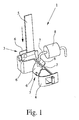
- a connecting device 1 which can be used to connect a not shown in detail according to the invention junction and junction box to a solar cell module.
- the connecting device 1 has a current bar 2 and two clamping devices 3, which are clamped on the current bar 2. In principle, more than two clamping devices 3 can be clamped on the current bar 2.
- the current bar 2 at a free end to a terminal 4, in the present case a tension spring clamp.
- the connection device 1 is arranged within the electrical connection and junction box and connected to the solar cell module via thin conductor strips 5.
- the clamping device 3 is designed and arranged for the production of a clamping contact such that at least one led out of the solar cell module thin conductor strip 5 in at least two different opposite insertion directions in the clamping device 3 can be inserted.
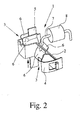
- FIGS. 1 and 2 wherein, according to FIG. 1, the conductor strip 5 is inserted from above into the clamping device 3 and according to FIG. 2 from below into the clamping device 3. After insertion of the conductor strip 5 in the clamping device 3, the conductor strip 5 is clamped between a clamping leg 6 of the clamping device 3 and the current bar 2.
- the clamping device 3 is designed and arranged such that both a clamping contact with at least one conductor strip 5 and a clamping contact with at least one preferably circular terminal conductor 7 of an electronic component by inserting of the conductor strip 5 and the lead 7 in the clamping device 3 can be produced.
- a circular connecting conductor 7 of a bypass diode 8 is inserted into a further clamping device 3, which is clamped to the current bar 2.
- the further clamping device 3 is clamped in the embodiments shown in FIGS. 1 and 2 at a free end of an angled conductor limb of the presently U-shaped current bar 2.
- the current bar 2 is web-shaped.
- the connecting device 1 only has a clamping device 3 for connection to a conductor strip 5 and a bypass diode 8, it is preferably provided for each conductor strip 5 and 8 for each diode 8 each provide a clamping device. This facilitates the connection of the conductor strip 5 to the terminal device.
- the clamping device 3 When inserting the connecting conductor 7 of the bypass diode 8 in the clamping device 3, the connecting conductor 7 is guided or clamped between a clamping leg 6 of the clamping device 3 and the current bar 2.
- the clamping device 3 has two cooperating clamping legs 6, wherein each clamping leg 6 has at least one outwardly curved, preferably cup-shaped, further insertion section 9 for the connecting conductor 7 in the clamping section and wherein according to FIG Embodiment of the further insertion section 9 of a clamping leg 6 and the further insertion section 9 of the other clamping leg 6 may be arranged opposite one another can.
- the cup-shaped bulge of the further insertion section 9 ensures that there is a secure clamping contact between the connecting conductor 7 and the current bar 2 after insertion of the connecting conductor 7 in the insertion section 9.
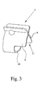
- FIGS. 1 and 2 one of the clamping devices 3 provided in FIGS. 1 and 2 for connection to the conductor strip 5 or to the connecting conductor 7 is shown in a schematic view from the side.
- the clamping device 3 is formed ⁇ -shaped and has two connected via a arranged in the bottom region of the clamping device 3 bottom portion 10 clamping legs 6, which converge toward one another in the direction of a clamping portion of the clamping device 3 and merge into diverging insertion bevels end, so that the clamping device 3 in Clamping portion has a substantially X-shaped cross-section.
- the clamping legs 6 are only partially connected via the bottom portion 10 with each other.
- a bottom-side insertion section 11 extends over which it is possible to introduce a conductor strip 5 from below in the direction of the clamping gap in the clamping device 3.
- the clamping legs 6 and / or the bottom portion 10 are made of a spring material to apply the clamping force necessary for clamping the clamping device 3 on the current bar 2 and the clamping of the conductor strip 5 and / or the connecting conductor 7.
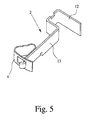
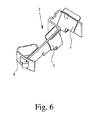
- FIG. 5 shows the current bar 2 of the connection device 1 shown in FIGS. 1 and 2.
- the current bar 2 is essentially U-shaped and has a straight conductor leg 12 and an angled conductor leg 13.
- the current bar 2 is bar-shaped formed, wherein at a free end of the angled conductor leg 13, the terminal 4 is provided.
- Fig. 6 the current bar 2 shown in Fig. 5 is shown again, wherein two clamping devices 3 are clamped on the current bar 2.
- the invention goes a completely new way by the flexible thin conductor strips 5 inserted both from above and from below into the housing of the electrical connection and junction box can be connected starting from two sides with the connecting device 1.
- a space-saving installation of the connection device 1 in the can is made possible by the provided in the connection and junction box according to the invention training the connection device 1.
- the bypass diodes 8 can be connected in a simple manner with the current bar 2 via a clamping device 3, wherein for connecting the conductor strips 5 and for connecting the connecting conductor 7 structurally identically designed clamping devices 3 can be used. Both contribute to the fact that a simple and secure connection out of the solar cell module led out thin conductor strips 5 is made possible.
Landscapes
- Photovoltaic Devices (AREA)
Abstract
Description
Die Erfindung betrifft eine elektrische Anschluß- und Verbindungsdose für ein Solarzellenmodul aus mit dünnen Leiterbändem angeschlossenen Solarzellen, mit einem Gehäuse und in dem Gehäuse vorgesehenen elektrischen oder/und elektronischen Einrichtungen sowie wenigstens einer in dem Gehäuse vorgesehenen und wenigstens eine Klemmeinrichtung aufweisenden elektrischen Anschlußvorrichtung.The invention relates to an electrical connection and junction box for a solar cell module connected to thin Leitererbändem solar cells, with a housing and provided in the housing electrical and / or electronic devices and at least one provided in the housing and at least one clamping device having electrical connection device.
Da die Ausgangsspannung einzelner Solarzellen im allgemeinen zu gering ist, um elektrische Geräte, wie Haushaltsgeräte oder ähnliche Geräte, zu betreiben, werden im allgemeinen mehrere Solarzellen zu Solarzellenmodulen zusammengeschaltet. Dabei besteht einerseits die Möglichkeit der Reihenschaltung der Solarzellen und andererseits die Möglichkeit der Parallelschaltung der Solarzellen im Solarzellenmodul. Durch ein Parallelschalten der Solarzellen addieren sich die einzelnen Ströme der Solarzellen zu einem Gesarntstrom. Dabei sollten die parallelgeschalteten Solarzellen allerdings im wesentlichen die gleichen physikalischen Eigenschaften haben, so daß sich in der Praxis das Parallelschalten von Solarzellen kaum durchgesetzt hat, insbesondere auch da eine einzelne Solarzelle bereits einen Strom von einigen Ampere liefern kann.Since the output voltage of individual solar cells is generally too low to operate electrical devices, such as household appliances or similar devices, several solar cells are generally interconnected to form solar cell modules. On the one hand there is the possibility of series connection of the solar cells and on the other hand the possibility of parallel connection of the solar cells in the solar cell module. By connecting the solar cells in parallel, the individual currents of the solar cells add up to a total flow. However, the parallel-connected solar cells should have substantially the same physical properties, so that the parallel connection of solar cells has hardly gained acceptance in practice, especially since a single solar cell can already supply a current of a few amperes.
Bei der Zusammenstellung von Solarzellenmodulen mit einzelnen Solarzellen werden die Solarzellen daher häufig in Reihe geschaltet. Ein Problem kann sich dabei jedoch dann ergeben, wenn ein Solarzellenmodul partiell abgeschattet wird, also eine Solarzelle oder einzelne Solarzellen des Solarzellenmoduls weniger oder gar keine Sonnenbestrahlung erhalten. Der Grund für eine verringerte Sonnenbestrahlung kann z. B. in einer Verschmutzung der Solarzellen oder in Schattenwürfen von Bäumen, Gebäudeeinrichtungen oder Gebäuden liegen.When assembling solar cell modules with individual solar cells, the solar cells are therefore often connected in series. However, a problem may arise when a solar cell module is partially shaded, that is to say a solar cell or individual solar cells of the solar cell module receive less or no solar radiation. The reason for a reduced sunlight can be z. B. in a pollution of the solar cells or shadows cast by trees, building facilities or buildings.
Im Gegensatz zu einer Abschattung des Solarmoduls gleichmäßig über seine gesamte Fläche, die nur zu einer Leistungsverringerung insgesamt führt, ergibt sich bei einer partiellen Abschattung folgendes Problem: Durch die in Reihe geschalteten Solarzellen des Solarzellenmoduls fließt ein gemeinsamer Strom, wobei jede einzelne Solarzelle mit ihrer jeweiligen Spannung zur Gesamtspannung des Solarzellenmoduls beiträgt. Wird nun eine Solarzelle abgeschattet, so erzeugt diese keine Spannung mehr und setzt dem Stromfluß im Solarzellenmodul praktisch eine Diode in Sperrichtung entgegen. Dies bedeutet jedoch, daß das gesamte Modul keinen Strom mehr liefern kann, so daß die gesamte Funktion des Solarzellenmoduls beeinträchtigt ist.In contrast to a shading of the solar module evenly over its entire surface, which leads only to a reduction in performance overall, resulting in a partial shading the following problem: Through the series-connected solar cells of the solar cell module flows a common current, each solar cell with their respective Voltage to the total voltage of the solar cell module contributes. If a solar cell is now shaded, it no longer generates any voltage and practically counteracts the current flow in the solar cell module by a diode in the reverse direction. However, this means that the entire module can no longer supply power, so that the entire function of the solar cell module is impaired.
Außerdem gilt, daß an der abgeschatteten Solarzelle eine Spannung anliegt, die abhängig ist von der Position der abgeschatteten Solarzelle in der Reihenschaltung. Ist diese an der abgeschatteten Solarzelle anliegende Spannung größer als ihre Sperrspannung, so wird es in der Solarzelle zu einem Durchschlag und damit zu einer dauerhaften Beschädigung der Solarzelle kommen. Selbst wenn es zu keiner Beschädigung der Solarzelle durch einen Durchschlag kommen sollte, wird in der abgeschatteten Solarzelle eine große Verlustleistung umgesetzt, so daß sich die abgeschattete Solarzelle aufheizt. Auch eine solche Aufheizung kann zu Beschädigungen an der abgeschatteten Solarzelle sowie an den ihr benachbarten Solarzellen führen.In addition, a voltage applied to the shaded solar cell depends on the position of the shaded solar cell in the series connection. If this voltage applied to the shaded solar cell is greater than its blocking voltage, a breakdown and thus permanent damage to the solar cell will occur in the solar cell. Even if there should be no damage to the solar cell by a breakdown, a large power loss is implemented in the shaded solar cell, so that heats up the shaded solar cell. Such heating can also lead to damage to the shaded solar cell and to the solar cells adjacent to it.
Um die mit teilweise abgeschatteten Solarzellen verbundene Problematik zu vermeiden, werden häufig Dioden, sogenannte Bypass-Dioden, verwendet, die antiparallel zu den Solarzellen geschaltet werden. Auf diese Weise wird erreicht, daß eine abgeschattete Solarzelle zwar keinen Anteil mehr zur Gesamtspannung des Solarzellenmoduls leistet, der Stromfluß jedoch trotzdem erhalten bleibt. Das Solarzellenmodul zeigt somit lediglich eine verminderte Betriebspannung, fällt jedoch nicht vollständig aus. Außerdem wird in der abgeschatteten Solarzelle keine Leistung mehr umgesetzt, so daß eine Beschädigung der abgeschatteten Solarzelle vermieden werden kann.In order to avoid the problems associated with partially shaded solar cells, diodes, so-called bypass diodes, are often used, which are connected in anti-parallel to the solar cells. In this way, it is achieved that a shaded solar cell does not contribute more to the total voltage of the solar cell module, but the current flow is still maintained. The solar cell module thus only shows a reduced operating voltage, but does not completely fail. In addition, no power is converted in the shaded solar cell, so that damage to the shaded solar cell can be avoided.
Grundsätzlich könnte jeder Solarzelle eines Solarzellenmoduls genau eine Diode zugeordnet sein. Häufig wird jedoch so vorgegangen, daß eine Mehrzahl hintereinander geschalteter Solarzellen jeweils durch eine gemeinsame Diode abgesichert wird. Elektrische Anschluß- und Verbindungsdosen, die für Solarzellenmodule verwendet werden, weisen somit im allgemeinen immer eine Mehrzahl von Bypass-Dioden auf Darüber hinaus können in den elektrischen Anschluß- und Verbindungsdosen weitere elektrische oder/und elektronische Einrichtungen vorgesehen sein, so daß der elektrischen Anschluß- und Verbindungsdose zugeführte Leiter mit den elektrischen oder/und elektronischen Einrichtungen, wie den Bypass-Dioden, verbunden werden müssen.In principle, each solar cell of a solar cell module could be associated with exactly one diode. Frequently, however, the procedure is such that a plurality of solar cells connected in series is respectively protected by a common diode. Electrical connection and connection boxes, which are used for solar cell modules, thus generally always have a plurality of bypass diodes in addition, in the electrical connection and connection boxes further electrical and / or electronic devices may be provided, so that the electrical connection and Junction fed conductor must be connected to the electrical and / or electronic devices, such as the bypass diodes.
Die Solarzellen in einem Solarzellenmodul sind im allgemeinen mit dünnen Leiterbändern, sogenannten Strings, miteinander verbunden. Diese Leiterbänder weisen typischerweise eine Dicke von wenigen Zehntel Millimeters (ca. 0,3 mm) und eine Breite von einigen Millimetern (ca. 3-8 mm) auf. Diese die einzelnen Solarzellen des Solarzellenmoduls miteinander verbindenden Leiterbänder werden aus dem Solarzellenmodul heraus geführt, so daß die dünnen Leiterbänder direkt zu Anschlußzwecken verwendet werden können.The solar cells in a solar cell module are generally connected to one another with thin conductor strips, so-called strings. These conductor strips typically have a thickness of a few tenths of a millimeter (about 0.3 mm) and a width of a few millimeters (about 3-8 mm). These individual solar cells of the solar cell module interconnecting conductor strips are guided out of the solar cell module, so that the thin conductor strips can be used directly for connection purposes.
Die Bypass-Dioden sind in der Regel auf einer Leiterplatte angeordnet, die mit einer Anschlußvorrichtung der Anschluß- und Verbindungsdose verbunden ist. Die Anschlußvorrichtung ist über wenigstens ein Leiterband mit dem Solarzellenmodul verbunden.The bypass diodes are usually arranged on a printed circuit board, which is connected to a connection device of the connection and junction box. The connecting device is connected via at least one conductor strip to the solar cell module.
Zum Anschluß werden die Leiterbänder typischerweise in die elektrische Anschluß- und Verbindungsdose von unten her eingeführt, die einen abnehmbaren Deckel aufweist, so daß die einzelnen Leiterbänder von Hand mit der in dem Gehäuse der Anschluß- und Verbindungsdose vorgesehenen elektrischen Anschlußvorrichtung kontaktiert werden können. Dazu werden die vom Solarzellenmodul, relativ zum Gehäuse der Anschluß- und Verbindungsdose von unten her kommenden dünnen Leiterbänder im allgemeinen um 180° umgebogen, um dann von oben her kommend beispielsweise über eine Klemmeinrichtung an die Anschlußvorrichtung angeschlossen zu werden. Ein solches Umbiegen ist ohne weiteres möglich, da die dünnen Leiterbänder, die typischerweise aus Metall bestehen, aufgrund ihrer Abmessungen, insbesondere nämlich ihrer geringen Dicke, sehr flexibel sind. Allerdings ist diese Vorgehensweise sehr aufwendig und zeitintensiv, und Anschlußfehler können nicht ohne weiteres vermieden werden. Darüber hinaus ist bei den bekannten Anschluß- und Verbindungsdosen von Nachteil, daß aufgrund der begrenzten äußeren Abmessungen des Gehäuses in der Regel im Inneren der Anschluß- und Verbindungsdose die elektrischen und/oder elektronischen Einrichtungen und die Anschlußvorrichtung sehr nah beieinander angeordnet werden müssen. Dadurch steht für den Anschluß der Leiterbänder ein nur sehr geringer Freiraum zur Verfügung, was den Anschluß erschwert.For connection, the conductor strips are typically inserted into the electrical connection and junction box from below, which has a removable cover, so that the individual conductor strips can be contacted by hand with the provided in the housing of the connection and junction box electrical connection device. These are the solar cell module, relative to the housing of the connection and junction box from below coming thin conductor strips generally bent by 180 °, to then be connected from above, for example, via a clamping device to the terminal device. Such a bending is readily possible, since the thin conductor strips, which are typically made of metal, are very flexible due to their dimensions, in particular their small thickness. However, this procedure is very complicated and time-consuming, and connection errors can not be avoided without further ado. Moreover, in the known connection and connection boxes of disadvantage that due to the limited outer dimensions of the housing usually inside the connection and junction box, the electrical and / or electronic devices and the connection device must be arranged very close to each other. As a result, only a very small space is available for the connection of the conductor strips, which complicates the connection.
Es ist daher die Aufgabe der Erfindung, eine solche elektrische Anschluß- und Verbindungsdose für ein Solarzellenmodul anzugeben, mit der ein einfacher und sicherer Anschluß aus dem Solarzellenmodul herausgeführter dünner Leiterbänder ermöglicht wird.It is therefore an object of the invention to provide such an electrical connection and junction box for a solar cell module, with a simple and secure connection out of the solar cell module led out thin conductor strips is made possible.
Ausgehend von der eingangs beschriebenen elektrischen Anschluß- und Verbindungsdose ist die zuvor hergeleitete und aufgezeigte Aufgabe bei einer ersten alternativen Ausführungsform der Erfindung dadurch gelöst, daß die Klemmeinrichtung zur Herstellung eines Klemmkontaktes zwischen der Anschlußvorrichtung und einem Leiterband derart ausgebildet und angeordnet ist, daß wenigstens ein aus dem Solarzellenmodul herausgeführtes dünnes Leiterband in zwei unterschiedlichen gegenüberliegenden Einführrichtungen in die Klemmeinrichtung einführbar ist.Starting from the electrical connection and junction box described above, the previously derived and indicated object is achieved in a first alternative embodiment of the invention in that the clamping device for producing a clamping contact between the terminal device and a conductor strip is designed and arranged such that at least one of led out of the solar cell module thin conductor strip in two different opposite insertion directions in the clamping device is inserted.
Die Erfindung geht also einen völlig neuen Weg, indem aus dem Solarzellenmodul herausgeführte und zum Anschluß der Solarzellen dienende dünne Leiterbänder erfindungsgemäß in zwei unterschiedlichen vorzugsweise gegenüberliegenden Einführrichtungen in die Klemmeinrichtung einführbar und damit an die elektrische Anschlußvorrichtung anschließbar sind. Durch die Erfindung ist es möglich, einerseits die zum Anschluß der Solarzellen dienenden dünnen Leiterbänder von unten her und andererseits von oben her in die Klemmeinrichtung einzuführen. Durch die Erfindung wird damit das aufwendige, aus dem Stand der Technik bekannte Vorgehen vermieden, die dünnen Leiterbänder zum Anschließen der Solarzellen in der Anschluß- und Verbindungsdose erst nach oben zu führen und dann um bis zu 180° umzubiegen, um sie der Anschlußvorrichtung zuzuführen. Beim Anschließen der Solarzellen des Solarzellenmoduls ist der erforderliche Aufwand also durch die Erfindung erheblich verringert. Dabei ist es erfindungsgemäß vorgesehen, daß bedarfsweise ein Leiterband von der einen oder von der anderen Seite der Klemmeinrichtung in die Klemmeinrichtung einführbar ist. Je nach der vorgegebenen Anordnung der Anschlußvorrichtung in dem Gehäuse kann es dabei vorgesehen sein, das Leiterband in der einen Einführrichtung oder in der anderen Einführrichtung in die Klemmeinrichtung einzuführen. Dadurch ergibt sich eine weitaus größere Flexibilität bei der Anordnung der Anschlußvorrichtung in einer erfindungsgemäßen Anschluß- und Verbindungsdose für ein Solarzellenmodul, Durch die erfindungsgemäße Anschluß- und Verbindungsdose wird darüber hinaus der Anschluß von aus dem Solarzellenmodul herausgeführten dünnen Leiterbänden weiter vereinfacht, da die erfindungsgemäße Anschluß-und Verbindungsdose von zwei Anschlußseiten her auf das Solarzellenmodul aufgesetzt werden kann, um die Leiterbänder von unten her in die elektrische Anschlußvorrichtung einzuführen.Thus, the invention goes a completely new way by leading out of the solar cell module and serving to connect the solar cells thin conductor strips according to the invention in two different preferably opposite insertion directions in the clamping device inserted and thus connectable to the electrical connection device. By means of the invention it is possible, on the one hand, to introduce the thin conductor strips serving to connect the solar cells from below and, on the other hand, from above, into the clamping device. The invention thus avoids the costly, known from the prior art approach to lead the thin conductor strips for connecting the solar cells in the connection and junction box only upwards and then bend by up to 180 ° to supply them to the terminal device. When connecting the solar cells of the solar cell module, the required effort is thus considerably reduced by the invention. It is inventively provided that, if necessary, a conductor strip from the one or from the other side of the clamping device is inserted into the clamping device. Depending on the predetermined arrangement of the connecting device in the housing, it may be provided to introduce the conductor strip in the one insertion direction or in the other insertion direction into the clamping device. This results in a much greater flexibility in the arrangement of the connection device in a connection and connection box according to the invention for a solar cell module, Through the connection and junction box according to the invention, moreover, the connection of lead out of the solar cell module thin conductor strips is further simplified, since the connection and junction box of the invention can be placed from two terminal sides on the solar cell module to the conductor strips from below into the electrical connection device introduce.
Die vorgenannte Aufgabe wird bei einer alternativen Ausführungsform der eingangs beschriebenen elektrischen Anschluß- und Verbindungsdose dadurch gelöst, daß die Klemmeinrichtung derart ausgebildet und angeordnet ist, daß sowohl ein Klemmkontakt mit wenigstens einem Leiterband als auch ein Klemmkontakt mit wenigstens einem vorzugsweise kreisförmigen Anschlußleiter eines elektronischen Bauteils, insbesondere einem Anschlußleiter einer Bypass-Diode, durch Einführen des Leiterbandes bzw, des Anschlußleiters in die Klemmeinrichtung herstellbar ist. Der Erfindung liegt an dieser Stelle der Grundgedanke zugrunde, eine Klemmeinrichtung sowohl für den Anschluß des Leiterbandes als auch für den Anschluß eines elektronischen Bauteils, wie beispielsweise einer Bypass-Diode, auszubilden.The above object is achieved in an alternative embodiment of the electrical connection and junction box described above in that the clamping device is designed and arranged such that both a terminal contact with at least one conductor strip and a terminal contact with at least one preferably circular terminal conductor of an electronic component, in particular a connecting conductor of a bypass diode, by introducing the conductor strip or, the connecting conductor in the clamping device can be produced. At this point, the invention is based on the basic idea of forming a clamping device both for the connection of the conductor strip and for the connection of an electronic component, such as a bypass diode.
Beispielsweise kann eine Mehrzahl von elektrischen Anschlußvorrichtungen in der Anschluß- und Verbindungsdose vorgesehen sein, die vorzugsweise nebeneinander angeordnet werden können. In diesem Fall ist es möglich, den ersten Anschlußleiter eines elektronischen Bauteils, vorzugsweise einer Bypass-Diode, in die Klemmeinrichtung einer ersten Anschlußvorrichtung und den zweiten Anschlußleiter des Bauteils in die Klemmeinrichtung einer benachbarten zweiten Anschlußvorrichtung einzuführen. In diesem Fall ist es nicht länger notwendig, beispielsweise die Bypass-Dioden auf einer Leiterplatte anzuordnen, wie dies üblicherweise bei den aus dem Stand der Technik bekannten Anschluß- und Verbindungsdosen vorgesehen ist. Dies trägt dazu bei, daß der im Inneren der Dose für den Anschluß der Leiterbänder zur Verfügung stehende Freiraum vergrößert wird, was den Anschluß erleichtert. Darüber hinaus ist von Vorteil, daß die bei der erfindungsgemäßen Anschluß- und Verbindungsdose vorgesehenen Klemmeinrichtungen bedarfsweise mit einem Leiterband und/oder mit einem Anschlußleiter eines elektronischen Bauteils verbunden werden können, was zu einem einfachen Aufbau der erfindungsgemäßen Anschluß- und Verbindungsdose und zu einer hohen Flexibilität bei der Anordnung der Anschlußvorrichtung in der erfindungsgemäßen Anschluß-und Verbindungsdose führt.For example, a plurality of electrical connection devices may be provided in the connection and connection box, which may preferably be arranged side by side. In this case, it is possible to insert the first lead of an electronic component, preferably a bypass diode, in the clamping device of a first terminal device and the second terminal conductor of the component in the clamping device of an adjacent second terminal device. In this case, it is no longer necessary to arrange, for example, the bypass diodes on a printed circuit board, as is usually provided in the connection and junction boxes known from the prior art. This helps to increase the free space available inside the can for connecting the conductor strips, which facilitates connection. Moreover, it is advantageous that the provided in the connection and junction box according to the invention clamping devices can be connected as needed with a conductor strip and / or with a terminal conductor of an electronic component, resulting in a simple construction of the junction box according to the invention and a high flexibility at the arrangement of the connection device in the connection and connection box according to the invention leads.
Bei einer besonders bevorzugten Ausführungsform ist vorgesehen, daß die Klemmeinrichtung Ω-förmig aussgebildet ist mit zwei über einen im Bodenbereich der Klemmeinrichtung angeordneten Bodenabschnitt verbundenen Klemmschenkeln, die in Richtung auf einen Klemmabschnitt der Klemmeinrichtung aufeinander zulaufen und endseitig in auseinanderlaufende Einführschrägen übergehen, so daß die Klemmeinrichtung im Klemmabschnitt einen im wesentlichen X-förmigen Querschnitt aufweist. Die Ω-förmige Ausbildung der Klemmeinrichtung trägt dazu bei, daß es in einfacher Weise möglich ist, ein Leiterband und/oder einen Anschlußleiter eines elektronischen Bauteils von oben her über die Einführschrägen in den Klemmabschnitt einzuführen. Darüber hinaus lassen sich Ω-förmige Klemmeinrichtungen in einfacher Weise herstellen und ermöglichen die sichere elektrische Kontaktierung der in den Klemmabschnitt eingeführten Leiter.In a particularly preferred embodiment, it is provided that the clamping device is formed Ω-shaped with two connected via a arranged in the bottom region of the clamping device bottom portion clamping legs which converge towards a clamping portion of the clamping device and the end pass into diverging insertion bevels, so that the clamping device in the clamping section has a substantially X-shaped cross-section. The Ω-shaped design of the clamping device contributes to the fact that it is possible in a simple manner to introduce a conductor strip and / or a terminal conductor of an electronic component from above via the insertion bevels in the clamping portion. In addition, Ω-shaped clamping devices can be produced in a simple manner and enable reliable electrical contacting of the conductors introduced into the clamping section.
Um ein Leiterband sowohl von oben her über die Einführschrägen als auch von unten her in den Klemmabschnitt der Klemmeinrichtung einführen zu können, kann es erfindungsgemäß vorgesehen sein, daß wenigstens ein bodenseitiger Einführabschnitt für ein Leiterband vorgesehen ist und daß im Bereich des Einführabschnittes die Klemmschenkel unverbunden sind. Vorzugsweise weist der Bodenabschnitt eine Ausnehmung auf, die zum Einführen eines Leiterbandes ausgebildet sein kann. Beispielsweise ist es möglich, daß sich der bodenseitige Einführabschnitt in Längsrichtung des Klemmabschnittes ausgehend von den Längsseiten der Klemmschenkel in Richtung zum mittleren Bereich der Klemmschenkel erstreckt. Grundsätzlich ist es natürlich auch möglich, daß der bodenseitige Einführabschnitt als schlitzförmige Ausnehmung des Bodenabschnitts ausgebildet ist. Bedarfsweise kann auch vorgesehen sein, daß der Bodenabschnitt mehrere in Längsrichtung nebeneinander liegende Einführabschnitte aufweist, die das Einführen eines Leiterbandes in die Klemmeinrichtung durch den Bodenabschnitt hindurch ermöglichen.In order to introduce a conductor strip both from above on the chamfers and from below into the clamping portion of the clamping device, it may be provided according to the invention that at least one bottom-side insertion section is provided for a conductor strip and that in the region of the insertion section, the clamping legs are unconnected , Preferably, the bottom portion has a recess which may be formed for insertion of a conductor strip. For example, it is possible that the bottom-side insertion section extends in the longitudinal direction of the clamping portion, starting from the longitudinal sides of the clamping legs in the direction of the central region of the clamping legs. In principle, it is of course also possible that the bottom-side insertion section is formed as a slot-shaped recess of the bottom portion. If necessary, it can also be provided that the bottom portion has a plurality of longitudinally adjacent insertion portions, which allow the insertion of a conductor strip in the clamping device through the bottom portion therethrough.
Um einen sicheren elektrischen Kontakt zwischen einem vorzugsweise kreisförmigen Anschlußleiter eines elektronischen Bauteils und der Klemmeinrichtung zu ermöglichen, kann erfindungsgemäß vorgesehen sein, daß der Klemmschenkel einer Klemmeinrichtung im Klemmabschnitt wenigstens einen nach außen gewölbten vorzugsweise schalenförmigen weiteren Einführabschnitt für den Anschlußleiter aufweist und daß, weiter vorzugsweise, der weitere Einführabschnitt des einen Klemmschenkels und der weitere Einführabschnitt des anderen Klemmschenkels gegenüberliegend angeordnet sind. Im letztgenannten Fall ergänzen sich die beiden gegenüberliegenden Einführabschnitte zu einer im wesentlichen nußförmigen Öffnung des Klemmabschnittes. Wird ein kreisförmiger Anschlußleiter in diesen Einführabschnitt eingeführt, wird durch die größere Kontaktfläche zwischen dem Anschlußleiter und dem Klemmschenkel eine sichere elektrische Kontaktierung gewährleistet.In order to enable a secure electrical contact between a preferably circular terminal conductor of an electronic component and the clamping device, it can be provided according to the invention that the Clamping leg of a clamping device in the clamping portion has at least one outwardly curved preferably cup-shaped further insertion section for the lead and that, more preferably, the further insertion of a clamping leg and the further insertion of the other clamping leg are arranged opposite one another. In the latter case, the two opposite insertion sections complement each other to form a substantially nut-shaped opening of the clamping portion. If a circular lead is introduced into this insertion, a secure electrical contact is ensured by the larger contact surface between the lead and the clamping leg.
Die Anschlußvorrichtung kann einen Strombalken aufweisen, auf den vorzugsweise zwei Klemmeinrichtungen derart aufgeklemmt sein können, daß über den Strombalken ein Leitungskontakt zwischen wenigstens einem in die erste Klemmeinrichtung eingeführten Leiterband und wenigstens einem in die zweite Klemmeinrichtung eingeführten Anschlußleiter, vorzugsweise einem Anschlußleiter einer Bypass-Diode, herstellbar ist. Nach dem Aufklemmen der Klemmeinrichtung auf den Strombalken verläuft der Strombalken zwischen dem Klemmabschnitt und wird zwischen zwei Klemmschenkeln eingeklemmt. Um ein Leiterband und/oder einen Anschlußleiter eines elektronischen Bauteils über die Klemmeinrichtung mit dem Strombalken zu verbinden, muß daß Leiterband und/oder der Anschlußleiter in den zwischen dem Strombalken und einem der Klemmschenkel gebildeten Klemmbereich eingeführt werden. Das Leiterband bzw. der Anschlußleiter werden somit zwischen dem Strombalken und einem Klemmschenkel der Klemmeinrichtung eingeklemmt.The connection device may comprise a current bar, to which preferably two clamping devices can be clamped in such a way that via the current bar a line contact between at least one conductor strip introduced into the first clamping device and at least one connecting conductor introduced into the second clamping device, preferably a connecting conductor of a bypass diode, can be produced. After clamping the clamping device on the current bar of the current bar runs between the clamping portion and is clamped between two clamping legs. In order to connect a conductor strip and / or a connecting conductor of an electronic component via the clamping device with the current bar, that conductor strip and / or the connecting conductor must be inserted into the clamping region formed between the current bar and one of the clamping legs. The conductor strip or the connecting conductor are thus clamped between the current bar and a clamping leg of the clamping device.
Der Strombalken kann stegförmig mit vorzugsweise im wesentlichen rechtwinklig zueinander angeordneten Stegendabschnitten ausgebildet sein. Vorzugsweise ist an beiden Stegendabschnitten jeweils eine Klemmeinrichtung vorgesehen, wobei weiter vorzugsweise in einem Anschlußzustand ein Leiterband an die eine Klemmeinrichtung und ein Anschlußleiter an die andere Klemmeinrichtung angeschlossen ist. Bei einer besonders bevorzugten Ausführungsform ist es vorgesehen, daß der Strombalken im wesentlichen U-förmig ausgebildet ist und einen geraden und einen abgewinkelten Leiterschenkel aufweist. An einem freien Ende des Leiterschenkels, vorzugsweise des abgewinkelten Leiterschenkels, kann eine Anschlußklemme vorgesehen sein zum Anschluß der Anschlußvorrichtung an einen Leitungskontakt, der aus der Anschluß- und Verbindungsdose herausführt. Vorzugsweise kann es sich bei der Anschlußklemme um eine Zugfederklemme handeln. Grundsätzlich können jedoch auch andere Formen von Anschlußklemmen eingesetzt werden. Wenngleich die zuvor beschriebene Ausbildung des Strombalkens einen besonders einfachen Einbau der Anschlußvorrichtung in das Gehäuse der Anschluß- und Verbindungsdose und einen vergleichsweise großen zum Anschluß der Leiterbänder zur Verfügung stehenden Freiraum sicherstellt, ist es grundsätzlich natürlich auch vorgesehen, den Strombalken in Abhängigkeit von der konstruktiven Ausgestaltung der Anschluß- und Verbindungsdose bzw. der Anordnung der in dem Gehäuse vorgesehenen elektrischen und/oder elektronischen Einrichtungen bedarfsweise an die tatsächlichen Platzverhältnisse anzupassen.The current bar may be web-shaped with preferably substantially mutually perpendicular web end sections. Preferably, a clamping device is provided in each case on both web end sections, moreover preferably in a connected state, a conductor strip is connected to the one clamping device and a connecting conductor to the other clamping device. In a particularly preferred embodiment, it is provided that the current bar is formed substantially U-shaped and has a straight and an angled conductor legs. At a free end of the ladder leg, preferably the angled conductor leg, a terminal may be provided for connection of the terminal device to a line contact, which leads out of the connection and junction box. Preferably, the terminal may be a tension spring clamp. In principle, however, other forms of terminals can be used. Although the above-described design of the current bar ensures a particularly simple installation of the connection device in the housing of the connection and junction box and a comparatively large space available for connecting the conductor strips available space, it is of course also provided, the current bar depending on the structural design the connection and junction box or the arrangement of provided in the housing electrical and / or electronic devices, if necessary, to adapt to the actual space conditions.
Die Klemmschenkel und/oder der Bodenabschnitt können aus einem Federmaterial hergestellt sein. Dies erleichtert die Herstellung und führt zu geringen Herstellungskosten. Grundsätzlich ist es aber auch möglich, daß die Klemmschenkel federbeaufschlagt sind, um eine ausreichende Klemmkraft im Bereich des Klemmabschnittes zur Verfügung zu stellen.The clamping legs and / or the bottom portion may be made of a spring material. This facilitates the production and leads to low production costs. In principle, however, it is also possible that the clamping legs are spring-loaded in order to provide a sufficient clamping force in the region of the clamping section.
Im einzelnen gibt es eine Vielzahl von Möglichkeiten, die erfindungsgemäße elektrische Anschluß- und Verbindungsdose auszugestalten und weiterzubilden, wobei einerseits auf die abhängigen Patentansprüche und andererseits auf die nachfolgende detaillierte Beschreibung eines bevorzugten Ausführungsbeispiels der Erfindung unter Bezugnahme auf die Zeichnung verwiesen wird. In der Zeichnung zeigt
- Fig. 1
- eine perspektivische Darstellung einer Anschlußvorrichtung mit zwei Klemmeinrichtungen zur Verwendung in einer erfindungsgemäßen Anschluß- und Verbindungsdose für ein Solarzellenmodul, wobei ein Leiterband von oben in eine Klemmeinrichtung der Anschlußvorrichtung eingeführt wird,
- Fig. 2
- die in Fig. 1 dargestellte Anschlußvorrichtung, wobei das Leiterband von unten in die Klemmeinrichtung eingeführt wird,
- Fig. 3
- eine Klemmeinrichtung der in den Fig. 1 und Fig. 2 dargestellten Anschlußvorrichtung in einer schematischen Ansicht von der Seite,
- Fig. 4
- die in Fig. 3 dargestellte Klemmeinrichtung in einer schematischen Ansicht von oben,
- Fig. 5
- einen eine Anschlußklemme aufweisenden Strombalken der in den Fig. 1 und Fig. 2 dargestellten Anschlußvorrichtung in einer schematischen Ansicht von oben und
- Fig. 6
- den in Fig. 5 dargestellten Strombalken mit zwei auf den Strombalken aufgeklemmten Klemmeinrichtungen der in den Fig. 3 und Fig. 4 dargestellten Art.
- Fig. 1
- a perspective view of a connecting device with two clamping devices for use in a junction box according to the invention for a solar cell module, wherein a conductor strip is inserted from above into a clamping device of the connecting device,
- Fig. 2
- the connection device shown in Fig. 1, wherein the conductor strip is inserted from below into the clamping device,
- Fig. 3
- a clamping device of the connecting device shown in FIGS. 1 and 2 in a schematic view from the side,
- Fig. 4
- the clamping device shown in Fig. 3 in a schematic view from above,
- Fig. 5
- a terminal having a current bar of the terminal device shown in FIGS. 1 and 2 in a schematic view from above and
- Fig. 6
- the current bar shown in Fig. 5 with two clamped on the current bar clamping devices of the type shown in FIGS. 3 and 4.
In Fig. 1 ist eine bevorzugte Ausführungsform einer Anschlußvorrichtung 1 dargestellt, die zum Anschluß einer nicht im einzelnen dargestellten erfindungsgemäßen Anschluß- und Verbindungsdose an ein Solarzellenmodul eingesetzt werden kann. Die Anschlußvorrichtung 1 weist einen Strombalken 2 und zwei Klemmeinrichtungen 3 auf, die auf den Strombalken 2 aufgeklemmt sind. Grundsätzlich können auch mehr als zwei Klemineinrichtungen 3 auf den Strombalken 2 aufgeklemmt sein. Darüber hinaus weist der Strombalken 2 an einem freien Ende eine Anschlußklemme 4 auf, im vorliegenden Fall eine Zugfederklemme. Im Einbauzustand ist die Anschlußvorrichtung 1 innerhalb der elektrischen Anschluß- und Verbindungsdose angeordnet und mit dem Solarzellenmodul über dünne Leiterbänder 5 verbunden.In Fig. 1, a preferred embodiment of a connecting
Um einen einfachen und sicheren Anschluß der aus dem Solarzellenmodul herausgeführten dünnen Leiterbänder 5 zu ermöglichen, ist es erfindungsgemäß vorgesehen, daß die Klemmeinrichtung 3 zur Herstellung eines Klemmkontaktes derart ausgebildet und angeordnet ist, daß wenigstens ein aus dem Solarzellenmodul herausgeführtes dünnes Leiterband 5 in wenigstens zwei unterschiedlichen gegenüberliegenden Einführrichtungen in die Klemmeinrichtung 3 einführbar ist. Dies wird bei einem Vergleich der Fig. 1 und 2 deutlich, wobei gemäß Fig. 1 das Leiterband 5 von oben her in die Klemmeinrichtung 3 und gemäß Fig. 2 von unten her in die Klemmeinrichtung 3 eingeführt wird. Nach dem Einführen des Leiterbandes 5 in die Klemmeinrichtung 3 ist das Leiterband 5 zwischen einem Klemmschenkel 6 der Klemmeinrichtung 3 und dem Strombalken 2 eingeklemmt.In order to enable a simple and secure connection of led out of the solar cell module thin conductor strips 5, it is provided according to the invention that the
Darüber hinaus ist aus den Fig. 1 und Fig. 2 zu entnehmen, daß die Klemmeinrichtung 3 derart ausgebildet und angeordnet ist, daß sowohl ein Klemmkontakt mit wenigstens einem Leiterband 5 als auch ein Klemmkontakt mit wenigstens einem vorzugsweise kreisförmigen Anschlußleiter 7 eines elektronischen Bauteils durch Einführen des Leiterbandes 5 bzw. des Anschlußleiters 7 in die Klemmeinrichtung 3 herstellbar ist. Gemäß den in Fig. 1 und Fig. 2 dargestellten Ausführungsformen ist ein kreisförmiger Anschlußleiter 7 einer Bypass-Diode 8 in eine weitere Klemmeinrichtung 3 eingeführt, die an den Strombalken 2 angeklemmt ist. Die weitere Klemmeinrichtung 3 ist bei der in den Fig. 1 und Fig. 2 dargestellten Ausführungsformen an einem freien Ende eines abgewinkelten Leiterschenkels des vorliegend U-förmig ausgebildeten Strombalkens 2 angeklemmt. Um das Aufschieben der Klemmeinrichtungen 3 auf den Strombalken 2 zu erleichtern, ist der Strombalken 2 stegförmig ausgebildet. Wenngleich es grundsätzlich auch möglich wäre, daß die Anschlußvorrichtung 1 lediglich eine Klemmeinrichtung 3 zum Anschluß an ein Leiterband 5 und an eine Bypass-Diode 8 aufweist, ist es vorzugsweise vorgesehen, für jedes Leiterband 5 und für jede Diode 8 jeweils eine Klemmeinrichtung 3 vorzusehen. Dies erleichtert das Anschließen des Leiterbandes 5 an die Anschlußvorrichtung 1.In addition, it can be seen from FIGS. 1 and 2 that the
Beim Einführen des Anschlußleiters 7 der Bypass-Diode 8 in die Klemmeinrichtung 3 wird der Anschlußleiter 7 zwischen einem Klemmschenkel 6 der Klemmeinrichtung 3 und dem Strombalken 2 geführt bzw. eingeklemmt. Wie sich insbesondere aus den Fig. 3 und Fig. 4 ergibt, weist die Klemmeinrichtung 3 zwei zusammenwirkende Klemmschenkel 6 auf, wobei jeder Klemmschenkel 6 im Klemmabschnitt wenigstens einen nach außen gewölbten vorzugsweise schalenförmigen weiteren Einführabschnitt 9 für den Anschlußleiter 7 aufweist und wobei gemäß der dargestellten Ausführungsform der weitere Einführabschnitt 9 des einen Klemmschenkels 6 und der weitere Einführabschnitt 9 des anderen Klemmschenkels 6 gegenüberliegend angeordnet sein können. Durch die schalenförmige Auswölbung des weiteren Einführabschnitts 9 wird gewährleistet, daß es zu einem sicheren Klemmkontakt zwischen dem Anschlußleiter 7 und dem Strombalken 2 nach dem Einführen des Anschlußleiters 7 in den Einführabschnitt 9 kommt.When inserting the connecting
In Fig. 3 ist eine der in den Fig. 1 und Fig. 2 zum Anschluß an das Leiterband 5 bzw. an den Anschlußleiter 7 vorgesehenen Klemmeinrichtungen 3 in einer schematischen Ansicht von der Seite dargestellt. Die Klemmeinrichtung 3 ist Ω-förmig ausgebildet und weist zwei über einen im Bodenbereich der Klemmeinrichtung 3 angeordneten Bodenabschnitt 10 verbundene Klemmschenkel 6 auf, die in Richtung auf einen Klemmabschnitt der Klemmeinrichtung 3 aufeinander zulaufen und endseitig in auseinanderlaufende Einführschrägen übergehen, so daß die Klemmeinrichtung 3 im Klemmabschnitt einen im wesentlichen X-förmigen Querschnitt aufweist. Durch die Einführschrägen am Ende der Klemmschenkel 6 wird das Einführen des Leiterbandes 5 und/oder des Anschlußleiters 7 erleichtert. Bei der in Fig. 3 dargestellten Ausführungsform einer Klemmeinrichtung 3 sind die Klemmschenkel 6 nur bereichsweise über den Bodenabschnitt 10 miteinander verbunden. Ausgehend von den Längsseiten der Klemmschenkel 6 in Richtung zum mittleren Bereich der Klemmschenkel 6 erstreckt sich ein bodenseitiger Einführabschnitt 11, über den es möglich ist, ein Leiterband 5 auch von unten her in Richtung zum Klemmspalt in die Klemmeinrichtung 3 einzuführen. Vorzugsweise sind die Klemmschenkel 6 und/oder der Bodenabschnitt 10 aus einem Federmaterial hergestellt, um die zum Aufklemmen der Klemmeinrichtung 3 auf den Strombalken 2 und die zum Einklemmen des Leiterbandes 5 und/oder des Anschlußleiters 7 notwendige Klemmkraft aufzubringen.3, one of the
Die Fig. 5 zeigt den in den Fig. 1 und Fig. 2 dargestellten Strombalken 2 der Anschlußvorrichtung 1. Der Strombalken 2 ist im wesentlichen U-förmig ausgebildet und weist einen geraden Leiterschenkel 12 und einen abgewinkelten Leiterschenkel 13 auf, Der Strombalken 2 ist stegförmig ausgebildet, wobei an einem freien Ende des abgewinkelten Leiterschenkels 13 die Anschlußklemme 4 vorgesehen ist. In Fig. 6 ist der in Fig. 5 dargestellte Strombalken 2 erneut dargestellt, wobei zwei Klemmeinrichtungen 3 auf den Strombalken 2 aufgeklemmt sind.FIG. 5 shows the
Wie der obigen Beschreibung der elektrischen Anschluß- und Verbindungsdose gemäß dem bevorzugten Ausführungsbeispiel entnehmbar ist, geht die Erfindung einen völlig neuen Weg, indem die flexiblen dünnen Leiterbänder 5 sowohl von oben als auch von unten her in das Gehäuse der elektrischen Anschluß- und Verbindungsdose eingeführt bzw. ausgehend von zwei Seiten mit der Anschlußvorrichtung 1 verbunden werden können. Darüber hinaus wird durch die bei der erfindungsgemäßen Anschluß- und Verbindungsdose vorgesehene Ausbildung der Anschlußvorrichtung 1 ein platzsparender Einbau der Anschlußvorrichtung 1 in die Dose ermöglicht. Im übrigen können die Bypass-Dioden 8 in einfacher Weise mit dem Strombalken 2 über eine Klemmeinrichtung 3 verbunden werden, wobei zum Anschluß der Leiterbänder 5 und zum Anschluß der Anschlußleiter 7 konstruktiv identisch ausgebildete Klemmeinrichtungen 3 eingesetzt werden können. Beides trägt dazu bei, daß ein einfacher und sicherer Anschluß aus dem Solarzellenmodul herausgeführter dünner Leiterbänder 5 ermöglicht wird.As the above description of the electrical connection and junction box according to the preferred embodiment can be removed, the invention goes a completely new way by the flexible thin conductor strips 5 inserted both from above and from below into the housing of the electrical connection and junction box can be connected starting from two sides with the connecting
Claims (11)
Applications Claiming Priority (1)
| Application Number | Priority Date | Filing Date | Title |
|---|---|---|---|
| DE102005025976A DE102005025976B4 (en) | 2005-06-03 | 2005-06-03 | Electrical connection and connection box for a solar cell module |
Publications (3)
| Publication Number | Publication Date |
|---|---|
| EP1729348A2 true EP1729348A2 (en) | 2006-12-06 |
| EP1729348A3 EP1729348A3 (en) | 2008-12-31 |
| EP1729348B1 EP1729348B1 (en) | 2010-10-06 |
Family
ID=36997258
Family Applications (1)
| Application Number | Title | Priority Date | Filing Date |
|---|---|---|---|
| EP06010045A Not-in-force EP1729348B1 (en) | 2005-06-03 | 2006-05-16 | Junction box for a solar cell modul |
Country Status (5)
| Country | Link |
|---|---|
| US (1) | US7530837B2 (en) |
| EP (1) | EP1729348B1 (en) |
| AT (1) | ATE484077T1 (en) |
| DE (2) | DE102005025976B4 (en) |
| ES (1) | ES2351799T3 (en) |
Cited By (9)
| Publication number | Priority date | Publication date | Assignee | Title |
|---|---|---|---|---|
| EP1976026A2 (en) * | 2007-03-28 | 2008-10-01 | Günther Spelsberg GmbH & Co. KG | Junction box |
| WO2009086874A1 (en) | 2008-01-08 | 2009-07-16 | Yamaichi Electronics Deutschland Gmbh | Socket, use, solar panel, contact element, and method |
| WO2009150104A3 (en) * | 2008-06-12 | 2010-10-07 | Anton Gensler Gmbh | Junction box for photovoltaic modules |
| WO2010054837A3 (en) * | 2008-11-14 | 2011-04-21 | Yamaichi Electronics Deutschland Gmbh | Solar panel, method for production and bridging socket |
| WO2011047570A1 (en) * | 2009-10-22 | 2011-04-28 | Lv Jikun | Junction box for photovoltaic component |
| WO2012168327A1 (en) * | 2011-06-08 | 2012-12-13 | Hirschmann Automotive Gmbh | Photovoltaic junction box with improved contacting |
| EP2579336A1 (en) * | 2011-10-06 | 2013-04-10 | Hosiden Corporation | Terminal box for solar cell module |
| TWI403047B (en) * | 2010-09-17 | 2013-07-21 | Delta Electronics Inc | Junction box and conductor strip connection device thereof |
| CN107820675A (en) * | 2015-06-29 | 2018-03-20 | 泰连公司 | Terminals for solar junction boxes |
Families Citing this family (42)
| Publication number | Priority date | Publication date | Assignee | Title |
|---|---|---|---|---|
| US7487771B1 (en) | 2004-09-24 | 2009-02-10 | Imaginit, Inc. | Solar panel frame assembly and method for forming an array of connected and framed solar panels |
| US20080283118A1 (en) * | 2007-05-17 | 2008-11-20 | Larankelo, Inc. | Photovoltaic ac inverter mount and interconnect |
| DE102007043178A1 (en) | 2007-09-11 | 2009-03-12 | Yamaichi Electronics Deutschland Gmbh | Junction box, solar panel, contact device and procedure |
| US20090084426A1 (en) * | 2007-09-28 | 2009-04-02 | Enphase Energy, Inc. | Universal interface for a photovoltaic module |
| EP2243168A2 (en) * | 2008-01-25 | 2010-10-27 | Applied Materials, Inc. | Automated solar cell electrical connection apparatus |
| TW200934025A (en) * | 2008-01-30 | 2009-08-01 | Sung Jung Minute Industry Co Ltd | Solar energy junction box composition |
| DE202008002426U1 (en) | 2008-02-21 | 2008-08-28 | Lumberg Connect Gmbh | Junction box for in particular photovoltaic panels |
| DE102008010375B4 (en) | 2008-02-21 | 2013-07-04 | Lumberg Connect Gmbh | Junction box for in particular photovoltaic panels |
| US7833033B2 (en) * | 2008-04-16 | 2010-11-16 | Molex Incorporated | Solar panel junction box and components thereof |
| DE102008020511A1 (en) * | 2008-04-23 | 2009-11-05 | Mc Technology Gmbh | Contact element for a connection terminal, connection terminal and jumper for a contact element |
| DE202008006120U1 (en) | 2008-05-03 | 2008-07-24 | Lumberg Connect Gmbh | Junction box for placement on a module |
| DE102008022051A1 (en) * | 2008-05-03 | 2009-11-19 | Lumberg Connect Gmbh | Junction box for a solar module |
| DE102008028462A1 (en) * | 2008-06-14 | 2009-12-17 | Kostal Industrie Elektrik Gmbh | Electrical connection and connection box for a solar cell module |
| DE102008032038A1 (en) * | 2008-06-27 | 2009-12-31 | Hager Electro Gmbh & Co. Kg | Connection device for connecting conductor to bus bar of distributor system, has clamp provided with clamp side pieces that are engaged to bus bar in clamping manner, and conductor clamped between one of side pieces and bus bar |
| DE102008039933B4 (en) * | 2008-08-27 | 2018-11-29 | Te Connectivity Germany Gmbh | Connecting device for connecting an electrical conductor with a solar module and method for their preparation, and solar module with such a connection device |
| DE102008062034B4 (en) * | 2008-12-12 | 2010-08-12 | Tyco Electronics Amp Gmbh | Connecting device for connection to a solar module and solar module with such a connection device |
| DE102009012539A1 (en) * | 2009-03-10 | 2010-09-23 | Tyco Electronics Amp Gmbh | Connecting device for connection to a solar module and solar module with such a connection device |
| US8435056B2 (en) * | 2009-04-16 | 2013-05-07 | Enphase Energy, Inc. | Apparatus for coupling power generated by a photovoltaic module to an output |
| WO2010123325A2 (en) * | 2009-04-24 | 2010-10-28 | 커넥스일렉트로닉스(주) | Smart junction box for a solar cell module |
| DE102009033481B4 (en) * | 2009-07-15 | 2012-07-05 | Phoenix Contact Gmbh & Co. Kg | Connection and connection device |
| CN102035157B (en) * | 2009-09-25 | 2013-02-27 | 无锡尚德太阳能电力有限公司 | Junction box for solar cell module and solar cell module |
| TWI449195B (en) * | 2009-10-01 | 2014-08-11 | Nexpower Technology Corp | Structure and method for connecting junction box to solar cell panel module |
| US20110220182A1 (en) * | 2010-03-12 | 2011-09-15 | Rfmarq, Inc. | Solar Panel Tracking and Performance Monitoring Through Wireless Communication |
| CN102208783B (en) * | 2010-03-31 | 2014-04-02 | 富士康(昆山)电脑接插件有限公司 | Junction box |
| CN102386258A (en) * | 2010-09-02 | 2012-03-21 | 国琏电子(上海)有限公司 | Junction box and solar system |
| TWI415355B (en) * | 2010-09-06 | 2013-11-11 | Ampower Technology Co Ltd | Junction box and solar power system |
| US8388358B2 (en) * | 2010-09-28 | 2013-03-05 | Tyco Electronics Corporation | Contact rail for a junction box |
| WO2012083049A1 (en) | 2010-12-17 | 2012-06-21 | First Solar, Inc | Electrical connection system |
| JP2014524231A (en) | 2011-07-18 | 2014-09-18 | エンフェイズ エナジー インコーポレイテッド | Elastic mounting assembly for photovoltaic modules |
| JP5729648B2 (en) * | 2011-10-13 | 2015-06-03 | ホシデン株式会社 | Terminal box for solar cell module |
| DE102012206731A1 (en) * | 2012-04-24 | 2013-10-24 | Tyco Electronics Amp Gmbh | Connecting device for a solar module |
| US20140120786A1 (en) | 2012-11-01 | 2014-05-01 | Avx Corporation | Single element wire to board connector |
| US8721376B1 (en) | 2012-11-01 | 2014-05-13 | Avx Corporation | Single element wire to board connector |
| USD734653S1 (en) | 2012-11-09 | 2015-07-21 | Enphase Energy, Inc. | AC module mounting bracket |
| CN203150720U (en) | 2013-02-28 | 2013-08-21 | 泰科电子(上海)有限公司 | Spring clamp and wire connection box |
| CN203456481U (en) * | 2013-07-16 | 2014-02-26 | 泰科电子(上海)有限公司 | Junction box |
| CN103390671B (en) * | 2013-07-25 | 2017-04-26 | 浙江鑫辉光伏科技有限公司 | Heat-dissipation optimization type photovoltaic terminal box |
| US9196973B2 (en) * | 2014-03-06 | 2015-11-24 | Chicony Power Technology Co., Ltd. | Solar junction box and wire connecting structure thereof |
| US9391386B2 (en) | 2014-10-06 | 2016-07-12 | Avx Corporation | Caged poke home contact |
| USD838674S1 (en) * | 2017-02-17 | 2019-01-22 | Landscape Forms, Inc. | Junction box for catenary light |
| US10320096B2 (en) | 2017-06-01 | 2019-06-11 | Avx Corporation | Flexing poke home contact |
| CN207977486U (en) * | 2018-01-23 | 2018-10-16 | 泰科电子(上海)有限公司 | Conducting terminal and connector assembly |
Citations (2)
| Publication number | Priority date | Publication date | Assignee | Title |
|---|---|---|---|---|
| EP1501133A1 (en) | 2003-07-21 | 2005-01-26 | Tyco Electronics AMP GmbH | Connecting box for connecting to a solar panel |
| EP1501157A2 (en) | 2003-07-21 | 2005-01-26 | Tyco Electronics AMP GmbH | Connecting box for a solar panel and solar panel |
Family Cites Families (12)
| Publication number | Priority date | Publication date | Assignee | Title |
|---|---|---|---|---|
| US3985414A (en) * | 1974-09-06 | 1976-10-12 | Electronics Stamping Corporation | Bus clip and bus strip construction |
| US3918788A (en) * | 1974-09-06 | 1975-11-11 | Electronics Stamping Corp | Bus clip and bus strip |
| US4813881A (en) * | 1986-12-29 | 1989-03-21 | Labinal Components And Systems, Inc. | Variable insertion force contact |
| US5816867A (en) * | 1996-08-22 | 1998-10-06 | Allen Bradley Company, Llc | Curved wire spring clamp with optimized bending stress distribution |
| DE19639785C2 (en) * | 1996-09-27 | 2001-06-13 | Weidmueller Interface | Busbar for terminal blocks, with a socket connector |
| WO2000030216A1 (en) * | 1998-11-17 | 2000-05-25 | Utilux Pty. Limited | Solar panel cable connector |
| EP1102354B1 (en) * | 1999-11-17 | 2008-05-28 | Tyco Electronics AMP GmbH | Apparatus for contacting foil conductors, in particular of a solar module |
| ES2306650T3 (en) * | 1999-11-17 | 2008-11-16 | Tyco Electronics Amp Gmbh | APPARATUS TO MAKE CONTACT WITH METAL SHEET DRIVERS, IN PARTICULAR THOSE OF A SOLAR MODULE. |
| KR100322350B1 (en) * | 2000-01-19 | 2002-02-07 | 윤흥식 | link strip for terminal |
| JP2002359389A (en) * | 2001-05-31 | 2002-12-13 | Kitani Denki Kk | Terminal box for photovoltaic module wiring |
| DE10315668B4 (en) * | 2002-08-28 | 2007-06-06 | Conrad Stanztechnik Gmbh | terminal |
| DE102004020958B3 (en) * | 2004-04-28 | 2005-08-25 | Rose Systemtechnik Gmbh | Terminal and thus formed junction box |
-
2005
- 2005-06-03 DE DE102005025976A patent/DE102005025976B4/en not_active Expired - Fee Related
-
2006
- 2006-05-16 DE DE502006008002T patent/DE502006008002D1/en active Active
- 2006-05-16 EP EP06010045A patent/EP1729348B1/en not_active Not-in-force
- 2006-05-16 ES ES06010045T patent/ES2351799T3/en active Active
- 2006-05-16 AT AT06010045T patent/ATE484077T1/en active
- 2006-06-02 US US11/421,955 patent/US7530837B2/en not_active Expired - Fee Related
Patent Citations (2)
| Publication number | Priority date | Publication date | Assignee | Title |
|---|---|---|---|---|
| EP1501133A1 (en) | 2003-07-21 | 2005-01-26 | Tyco Electronics AMP GmbH | Connecting box for connecting to a solar panel |
| EP1501157A2 (en) | 2003-07-21 | 2005-01-26 | Tyco Electronics AMP GmbH | Connecting box for a solar panel and solar panel |
Cited By (10)
| Publication number | Priority date | Publication date | Assignee | Title |
|---|---|---|---|---|
| EP1976026A2 (en) * | 2007-03-28 | 2008-10-01 | Günther Spelsberg GmbH & Co. KG | Junction box |
| WO2009086874A1 (en) | 2008-01-08 | 2009-07-16 | Yamaichi Electronics Deutschland Gmbh | Socket, use, solar panel, contact element, and method |
| US8075326B2 (en) | 2008-01-08 | 2011-12-13 | Yamaichi Electronics Co., Ltd. | Junction box and contact element for photovoltaic modules |
| WO2009150104A3 (en) * | 2008-06-12 | 2010-10-07 | Anton Gensler Gmbh | Junction box for photovoltaic modules |
| WO2010054837A3 (en) * | 2008-11-14 | 2011-04-21 | Yamaichi Electronics Deutschland Gmbh | Solar panel, method for production and bridging socket |
| WO2011047570A1 (en) * | 2009-10-22 | 2011-04-28 | Lv Jikun | Junction box for photovoltaic component |
| TWI403047B (en) * | 2010-09-17 | 2013-07-21 | Delta Electronics Inc | Junction box and conductor strip connection device thereof |
| WO2012168327A1 (en) * | 2011-06-08 | 2012-12-13 | Hirschmann Automotive Gmbh | Photovoltaic junction box with improved contacting |
| EP2579336A1 (en) * | 2011-10-06 | 2013-04-10 | Hosiden Corporation | Terminal box for solar cell module |
| CN107820675A (en) * | 2015-06-29 | 2018-03-20 | 泰连公司 | Terminals for solar junction boxes |
Also Published As
| Publication number | Publication date |
|---|---|
| EP1729348A3 (en) | 2008-12-31 |
| US7530837B2 (en) | 2009-05-12 |
| EP1729348B1 (en) | 2010-10-06 |
| DE102005025976B4 (en) | 2007-03-15 |
| DE102005025976A1 (en) | 2006-12-14 |
| DE502006008002D1 (en) | 2010-11-18 |
| US20060289053A1 (en) | 2006-12-28 |
| ES2351799T3 (en) | 2011-02-10 |
| ATE484077T1 (en) | 2010-10-15 |
Similar Documents
| Publication | Publication Date | Title |
|---|---|---|
| EP1729348B1 (en) | Junction box for a solar cell modul | |
| DE10358140B4 (en) | Electrical connection and connection box for a solar cell module | |
| DE4411306C1 (en) | Electrical connecting terminal, in particular a modular terminal, having a plug link, as well as such a plug link | |
| DE10351289B4 (en) | Jumper for electrical connection and / or connection terminals | |
| DE202010018062U1 (en) | Connection and connection device | |
| DE102007051419A1 (en) | NH fuse switch disconnector with current transformer | |
| EP3375048B1 (en) | Plug contact | |
| DE102014113086A1 (en) | Clamping cage for a direct plug-in terminal | |
| DE112012005983T5 (en) | Assembly or assembly group for fixing a solar module wire and a solar module that uses this | |
| DE202017100907U1 (en) | clamp | |
| EP1672702B1 (en) | Junction box for a solar cell modul | |
| DE19963268B4 (en) | Fuse block, associated fuse box and manufacturing process | |
| WO2008095453A1 (en) | Electrical appliance and appliance arrangement | |
| EP2429037B1 (en) | Frame clamp element for electromechanical switching devices with integrated connection piece | |
| DE2251020C3 (en) | Connection device | |
| DE69602489T2 (en) | Multipole DC motor | |
| DE202014101856U1 (en) | Quick terminal | |
| DE1919169U (en) | DEVICE FOR CONNECTING AND CLAMPING ELECTRICAL LADDERS. | |
| EP2284953A1 (en) | Electro-installation device and method for mounting the same | |
| DE19944427A1 (en) | Cable connection between ribbon cable and round ribbon cable or round cable and method for their production | |
| DE102008039932A1 (en) | Connecting device for connecting an electrical conductor with a solar module and method for their preparation, and solar module with such a connection device | |
| DE1929903C3 (en) | Hot wire relay | |
| DE4026037A1 (en) | CONNECTING TERMINAL | |
| DE1815081U (en) | LOETOESE FOR PRINTED CIRCUITS APPLIED TO AN INSULATION PLATE. | |
| DE3004874A1 (en) | Component board for miniature electrical appliance - has support plate with slotted gaps with sections bridged by flat shorting strips |
Legal Events
| Date | Code | Title | Description |
|---|---|---|---|
| PUAI | Public reference made under article 153(3) epc to a published international application that has entered the european phase |
Free format text: ORIGINAL CODE: 0009012 |
|
| AK | Designated contracting states |
Kind code of ref document: A2 Designated state(s): AT BE BG CH CY CZ DE DK EE ES FI FR GB GR HU IE IS IT LI LT LU LV MC NL PL PT RO SE SI SK TR |
|
| AX | Request for extension of the european patent |
Extension state: AL BA HR MK YU |
|
| PUAL | Search report despatched |
Free format text: ORIGINAL CODE: 0009013 |
|
| AK | Designated contracting states |
Kind code of ref document: A3 Designated state(s): AT BE BG CH CY CZ DE DK EE ES FI FR GB GR HU IE IS IT LI LT LU LV MC NL PL PT RO SE SI SK TR |
|
| AX | Request for extension of the european patent |
Extension state: AL BA HR MK YU |
|
| 17P | Request for examination filed |
Effective date: 20090630 |
|
| AKX | Designation fees paid |
Designated state(s): AT BE BG CH CY CZ DE DK EE ES FI FR GB GR HU IE IS IT LI LT LU LV MC NL PL PT RO SE SI SK TR |
|
| 17Q | First examination report despatched |
Effective date: 20100304 |
|
| GRAP | Despatch of communication of intention to grant a patent |
Free format text: ORIGINAL CODE: EPIDOSNIGR1 |
|
| GRAS | Grant fee paid |
Free format text: ORIGINAL CODE: EPIDOSNIGR3 |
|
| GRAA | (expected) grant |
Free format text: ORIGINAL CODE: 0009210 |
|
| AK | Designated contracting states |
Kind code of ref document: B1 Designated state(s): AT BE BG CH CY CZ DE DK EE ES FI FR GB GR HU IE IS IT LI LT LU LV MC NL PL PT RO SE SI SK TR |
|
| REG | Reference to a national code |
Ref country code: GB Ref legal event code: FG4D Free format text: NOT ENGLISH |
|
| REG | Reference to a national code |
Ref country code: CH Ref legal event code: EP |
|
| REG | Reference to a national code |
Ref country code: IE Ref legal event code: FG4D Free format text: LANGUAGE OF EP DOCUMENT: GERMAN |
|
| REF | Corresponds to: |
Ref document number: 502006008002 Country of ref document: DE Date of ref document: 20101118 Kind code of ref document: P |
|
| REG | Reference to a national code |
Ref country code: NL Ref legal event code: VDEP Effective date: 20101006 |
|
| REG | Reference to a national code |
Ref country code: ES Ref legal event code: FG2A Effective date: 20110131 |
|
| PG25 | Lapsed in a contracting state [announced via postgrant information from national office to epo] |
Ref country code: SI Free format text: LAPSE BECAUSE OF FAILURE TO SUBMIT A TRANSLATION OF THE DESCRIPTION OR TO PAY THE FEE WITHIN THE PRESCRIBED TIME-LIMIT Effective date: 20101006 |
|
| LTIE | Lt: invalidation of european patent or patent extension |
Effective date: 20101006 |
|
| REG | Reference to a national code |
Ref country code: IE Ref legal event code: FD4D |
|
| PG25 | Lapsed in a contracting state [announced via postgrant information from national office to epo] |
Ref country code: LT Free format text: LAPSE BECAUSE OF FAILURE TO SUBMIT A TRANSLATION OF THE DESCRIPTION OR TO PAY THE FEE WITHIN THE PRESCRIBED TIME-LIMIT Effective date: 20101006 |
|
| PG25 | Lapsed in a contracting state [announced via postgrant information from national office to epo] |
Ref country code: SE Free format text: LAPSE BECAUSE OF FAILURE TO SUBMIT A TRANSLATION OF THE DESCRIPTION OR TO PAY THE FEE WITHIN THE PRESCRIBED TIME-LIMIT Effective date: 20101006 Ref country code: LV Free format text: LAPSE BECAUSE OF FAILURE TO SUBMIT A TRANSLATION OF THE DESCRIPTION OR TO PAY THE FEE WITHIN THE PRESCRIBED TIME-LIMIT Effective date: 20101006 Ref country code: PT Free format text: LAPSE BECAUSE OF FAILURE TO SUBMIT A TRANSLATION OF THE DESCRIPTION OR TO PAY THE FEE WITHIN THE PRESCRIBED TIME-LIMIT Effective date: 20110207 Ref country code: FI Free format text: LAPSE BECAUSE OF FAILURE TO SUBMIT A TRANSLATION OF THE DESCRIPTION OR TO PAY THE FEE WITHIN THE PRESCRIBED TIME-LIMIT Effective date: 20101006 Ref country code: BG Free format text: LAPSE BECAUSE OF FAILURE TO SUBMIT A TRANSLATION OF THE DESCRIPTION OR TO PAY THE FEE WITHIN THE PRESCRIBED TIME-LIMIT Effective date: 20110106 Ref country code: NL Free format text: LAPSE BECAUSE OF FAILURE TO SUBMIT A TRANSLATION OF THE DESCRIPTION OR TO PAY THE FEE WITHIN THE PRESCRIBED TIME-LIMIT Effective date: 20101006 Ref country code: IS Free format text: LAPSE BECAUSE OF FAILURE TO SUBMIT A TRANSLATION OF THE DESCRIPTION OR TO PAY THE FEE WITHIN THE PRESCRIBED TIME-LIMIT Effective date: 20110206 |
|
| PG25 | Lapsed in a contracting state [announced via postgrant information from national office to epo] |
Ref country code: IE Free format text: LAPSE BECAUSE OF FAILURE TO SUBMIT A TRANSLATION OF THE DESCRIPTION OR TO PAY THE FEE WITHIN THE PRESCRIBED TIME-LIMIT Effective date: 20101006 Ref country code: EE Free format text: LAPSE BECAUSE OF FAILURE TO SUBMIT A TRANSLATION OF THE DESCRIPTION OR TO PAY THE FEE WITHIN THE PRESCRIBED TIME-LIMIT Effective date: 20101006 Ref country code: CZ Free format text: LAPSE BECAUSE OF FAILURE TO SUBMIT A TRANSLATION OF THE DESCRIPTION OR TO PAY THE FEE WITHIN THE PRESCRIBED TIME-LIMIT Effective date: 20101006 |
|
| PLBE | No opposition filed within time limit |
Free format text: ORIGINAL CODE: 0009261 |
|
| STAA | Information on the status of an ep patent application or granted ep patent |
Free format text: STATUS: NO OPPOSITION FILED WITHIN TIME LIMIT |
|
| PG25 | Lapsed in a contracting state [announced via postgrant information from national office to epo] |
Ref country code: PL Free format text: LAPSE BECAUSE OF FAILURE TO SUBMIT A TRANSLATION OF THE DESCRIPTION OR TO PAY THE FEE WITHIN THE PRESCRIBED TIME-LIMIT Effective date: 20101006 Ref country code: SK Free format text: LAPSE BECAUSE OF FAILURE TO SUBMIT A TRANSLATION OF THE DESCRIPTION OR TO PAY THE FEE WITHIN THE PRESCRIBED TIME-LIMIT Effective date: 20101006 Ref country code: DK Free format text: LAPSE BECAUSE OF FAILURE TO SUBMIT A TRANSLATION OF THE DESCRIPTION OR TO PAY THE FEE WITHIN THE PRESCRIBED TIME-LIMIT Effective date: 20101006 Ref country code: RO Free format text: LAPSE BECAUSE OF FAILURE TO SUBMIT A TRANSLATION OF THE DESCRIPTION OR TO PAY THE FEE WITHIN THE PRESCRIBED TIME-LIMIT Effective date: 20101006 |
|
| 26N | No opposition filed |
Effective date: 20110707 |
|
| REG | Reference to a national code |
Ref country code: DE Ref legal event code: R097 Ref document number: 502006008002 Country of ref document: DE Effective date: 20110707 |
|
| BERE | Be: lapsed |
Owner name: GUNTHER SPELSBERG G.M.B.H. & CO. KG Effective date: 20110531 |
|
| PG25 | Lapsed in a contracting state [announced via postgrant information from national office to epo] |
Ref country code: MC Free format text: LAPSE BECAUSE OF NON-PAYMENT OF DUE FEES Effective date: 20110531 |
|
| GBPC | Gb: european patent ceased through non-payment of renewal fee |
Effective date: 20110516 |
|
| PG25 | Lapsed in a contracting state [announced via postgrant information from national office to epo] |
Ref country code: BE Free format text: LAPSE BECAUSE OF NON-PAYMENT OF DUE FEES Effective date: 20110531 |
|
| PG25 | Lapsed in a contracting state [announced via postgrant information from national office to epo] |
Ref country code: GB Free format text: LAPSE BECAUSE OF NON-PAYMENT OF DUE FEES Effective date: 20110516 |
|
| PGFP | Annual fee paid to national office [announced via postgrant information from national office to epo] |
Ref country code: AT Payment date: 20120511 Year of fee payment: 7 |
|
| PG25 | Lapsed in a contracting state [announced via postgrant information from national office to epo] |
Ref country code: LU Free format text: LAPSE BECAUSE OF NON-PAYMENT OF DUE FEES Effective date: 20110516 Ref country code: CY Free format text: LAPSE BECAUSE OF FAILURE TO SUBMIT A TRANSLATION OF THE DESCRIPTION OR TO PAY THE FEE WITHIN THE PRESCRIBED TIME-LIMIT Effective date: 20101006 |
|
| PGFP | Annual fee paid to national office [announced via postgrant information from national office to epo] |
Ref country code: CH Payment date: 20130523 Year of fee payment: 8 |
|
| PGFP | Annual fee paid to national office [announced via postgrant information from national office to epo] |
Ref country code: GR Payment date: 20130521 Year of fee payment: 8 |
|
| PG25 | Lapsed in a contracting state [announced via postgrant information from national office to epo] |
Ref country code: TR Free format text: LAPSE BECAUSE OF FAILURE TO SUBMIT A TRANSLATION OF THE DESCRIPTION OR TO PAY THE FEE WITHIN THE PRESCRIBED TIME-LIMIT Effective date: 20101006 |
|
| PG25 | Lapsed in a contracting state [announced via postgrant information from national office to epo] |
Ref country code: HU Free format text: LAPSE BECAUSE OF FAILURE TO SUBMIT A TRANSLATION OF THE DESCRIPTION OR TO PAY THE FEE WITHIN THE PRESCRIBED TIME-LIMIT Effective date: 20101006 |
|
| REG | Reference to a national code |
Ref country code: AT Ref legal event code: MM01 Ref document number: 484077 Country of ref document: AT Kind code of ref document: T Effective date: 20130531 |
|
| PG25 | Lapsed in a contracting state [announced via postgrant information from national office to epo] |
Ref country code: AT Free format text: LAPSE BECAUSE OF NON-PAYMENT OF DUE FEES Effective date: 20130531 |
|
| REG | Reference to a national code |
Ref country code: CH Ref legal event code: PL |
|
| PG25 | Lapsed in a contracting state [announced via postgrant information from national office to epo] |
Ref country code: LI Free format text: LAPSE BECAUSE OF NON-PAYMENT OF DUE FEES Effective date: 20140531 Ref country code: GR Free format text: LAPSE BECAUSE OF NON-PAYMENT OF DUE FEES Effective date: 20141203 Ref country code: CH Free format text: LAPSE BECAUSE OF NON-PAYMENT OF DUE FEES Effective date: 20140531 |
|
| REG | Reference to a national code |
Ref country code: GR Ref legal event code: ML Ref document number: 20100402968 Country of ref document: GR Effective date: 20141203 |
|
| REG | Reference to a national code |
Ref country code: GR Ref legal event code: EP Ref document number: 20100402968 Country of ref document: GR Effective date: 20110119 |
|
| REG | Reference to a national code |
Ref country code: FR Ref legal event code: PLFP Year of fee payment: 11 |
|
| REG | Reference to a national code |
Ref country code: FR Ref legal event code: PLFP Year of fee payment: 12 |
|
| REG | Reference to a national code |
Ref country code: FR Ref legal event code: PLFP Year of fee payment: 13 |
|
| PGFP | Annual fee paid to national office [announced via postgrant information from national office to epo] |
Ref country code: ES Payment date: 20180626 Year of fee payment: 13 Ref country code: DE Payment date: 20180529 Year of fee payment: 13 |
|
| PGFP | Annual fee paid to national office [announced via postgrant information from national office to epo] |
Ref country code: FR Payment date: 20180522 Year of fee payment: 13 Ref country code: IT Payment date: 20180530 Year of fee payment: 13 |
|
| REG | Reference to a national code |
Ref country code: DE Ref legal event code: R119 Ref document number: 502006008002 Country of ref document: DE |
|
| PG25 | Lapsed in a contracting state [announced via postgrant information from national office to epo] |
Ref country code: DE Free format text: LAPSE BECAUSE OF NON-PAYMENT OF DUE FEES Effective date: 20191203 Ref country code: IT Free format text: LAPSE BECAUSE OF NON-PAYMENT OF DUE FEES Effective date: 20190516 |
|
| PG25 | Lapsed in a contracting state [announced via postgrant information from national office to epo] |
Ref country code: FR Free format text: LAPSE BECAUSE OF NON-PAYMENT OF DUE FEES Effective date: 20190531 |
|
| REG | Reference to a national code |
Ref country code: ES Ref legal event code: FD2A Effective date: 20200930 |
|
| PG25 | Lapsed in a contracting state [announced via postgrant information from national office to epo] |
Ref country code: ES Free format text: LAPSE BECAUSE OF NON-PAYMENT OF DUE FEES Effective date: 20190517 |