EP1501133A1 - Connecting box for connecting to a solar panel - Google Patents
Connecting box for connecting to a solar panel Download PDFInfo
- Publication number
- EP1501133A1 EP1501133A1 EP04015562A EP04015562A EP1501133A1 EP 1501133 A1 EP1501133 A1 EP 1501133A1 EP 04015562 A EP04015562 A EP 04015562A EP 04015562 A EP04015562 A EP 04015562A EP 1501133 A1 EP1501133 A1 EP 1501133A1
- Authority
- EP
- European Patent Office
- Prior art keywords
- circuit board
- printed circuit
- connecting box
- contact
- contact elements
- Prior art date
- Legal status (The legal status is an assumption and is not a legal conclusion. Google has not performed a legal analysis and makes no representation as to the accuracy of the status listed.)
- Granted
Links
- 239000012790 adhesive layer Substances 0.000 claims abstract description 21
- 239000011888 foil Substances 0.000 claims description 9
- 239000000853 adhesive Substances 0.000 claims description 4
- 230000001070 adhesive effect Effects 0.000 claims description 4
- 239000004020 conductor Substances 0.000 abstract description 33
- 238000003780 insertion Methods 0.000 description 3
- 230000037431 insertion Effects 0.000 description 3
- 238000000034 method Methods 0.000 description 3
- 238000010276 construction Methods 0.000 description 2
- 230000017525 heat dissipation Effects 0.000 description 2
- 230000001419 dependent effect Effects 0.000 description 1
- 239000010410 layer Substances 0.000 description 1
- 239000002184 metal Substances 0.000 description 1
- 239000007769 metal material Substances 0.000 description 1
- 230000002093 peripheral effect Effects 0.000 description 1
Images

Classifications
-
- H—ELECTRICITY
- H02—GENERATION; CONVERSION OR DISTRIBUTION OF ELECTRIC POWER
- H02S—GENERATION OF ELECTRIC POWER BY CONVERSION OF INFRARED RADIATION, VISIBLE LIGHT OR ULTRAVIOLET LIGHT, e.g. USING PHOTOVOLTAIC [PV] MODULES
- H02S40/00—Components or accessories in combination with PV modules, not provided for in groups H02S10/00 - H02S30/00
- H02S40/30—Electrical components
- H02S40/34—Electrical components comprising specially adapted electrical connection means to be structurally associated with the PV module, e.g. junction boxes
-
- H—ELECTRICITY
- H01—ELECTRIC ELEMENTS
- H01R—ELECTRICALLY-CONDUCTIVE CONNECTIONS; STRUCTURAL ASSOCIATIONS OF A PLURALITY OF MUTUALLY-INSULATED ELECTRICAL CONNECTING ELEMENTS; COUPLING DEVICES; CURRENT COLLECTORS
- H01R9/00—Structural associations of a plurality of mutually-insulated electrical connecting elements, e.g. terminal strips or terminal blocks; Terminals or binding posts mounted upon a base or in a case; Bases therefor
- H01R9/22—Bases, e.g. strip, block, panel
- H01R9/24—Terminal blocks
- H01R9/2458—Electrical interconnections between terminal blocks
- H01R9/2466—Electrical interconnections between terminal blocks using a planar conductive structure, e.g. printed circuit board
-
- Y—GENERAL TAGGING OF NEW TECHNOLOGICAL DEVELOPMENTS; GENERAL TAGGING OF CROSS-SECTIONAL TECHNOLOGIES SPANNING OVER SEVERAL SECTIONS OF THE IPC; TECHNICAL SUBJECTS COVERED BY FORMER USPC CROSS-REFERENCE ART COLLECTIONS [XRACs] AND DIGESTS
- Y02—TECHNOLOGIES OR APPLICATIONS FOR MITIGATION OR ADAPTATION AGAINST CLIMATE CHANGE
- Y02E—REDUCTION OF GREENHOUSE GAS [GHG] EMISSIONS, RELATED TO ENERGY GENERATION, TRANSMISSION OR DISTRIBUTION
- Y02E10/00—Energy generation through renewable energy sources
- Y02E10/50—Photovoltaic [PV] energy
Abstract
Description
- The invention relates to a connecting box for connection to a solar panel according to the preamble of
claim 1. Connecting boxes are used in a wide variety of technical sectors in order to make an electrical connections between electric lines and an electrical device. - Solar panels have a large number of solar cells which are used to obtain power from sunlight. The electric voltage generated by the solar cells is conveyed via electric lines, for example to a rectifier, for feeding into an alternating voltage network or to a battery. A connecting box is provided for conveying and for electrical contacting of the lines of the solar panel.
- A corresponding connecting box is known from European
patent application EP 1 102 354 A2. The connecting box has a housing, in the base board of which is provided an opening for introducing the electric lines of the solar panel. Electrical contacts for contacting the electric lines are provided in the connecting box. The electrical contacts are in turn connected to terminal pins which are arranged in a side wall of the housing and are used for connecting electric lines. The connected electric lines lead to the rectifier or to the battery. Conductor rails comprising a contact region for detachable connection of a foil conductor of the solar panel are provided in the housing as the electrical contacts. The contact region comprises a metal clamping spring to which the foil contact can be securely clamped. For introducing the foil contact, the clamping spring is opened in a clamping region by means of a tool, then the foil contact is introduced into the clamping spring and the tool then removed from the clamping spring, so the clamping spring recoils into the starting position and in the process securely clamps the foil contact. - The known connecting box has the drawback that components which are connected to the electrical contact elements of the connecting box are relatively complex to assemble.
- The object of the invention consists in providing an improved connecting box.
- The object of the invention is achieved by the connecting box according to
claim 1. - Further advantageous embodiments of the invention are given in the dependent claims.
- The connecting box according to
claim 1 has the advantage that a printed circuit board is provided on which the components are arranged and the printed circuit board is held in the housing. Simple assembly and disassembly of a plurality of components is simultaneously possible as a result of the arrangement of the printed circuit board. In addition, the heat generated by the components can be better dissipated as a result of the printed circuit board. - In one advantageous embodiment the printed circuit board is inserted and held in holding recesses of the contact elements. Is therefore not necessary to provide new holding recesses, for example in the housing of the connecting box. The printed circuit board comprises appropriate holding elements for holding purposes.
- In a preferred embodiment, the printed circuit board is held in the connecting box by an adhesive layer. The use of the adhesive layer provides a simple and secure connecting technique between the printed circuit board and the connecting box.
- In a preferred embodiment, the adhesive layer is formed from a heat conducting material. The heat generated by the components can therefore be conveyed via the printed circuit board and the adhesive layer to the connecting box or the cover of the connecting box. Improved heat dissipation is thus possible.
- In a further advantageous embodiment the adhesive layer is constructed as a heat conducting adhesive foil. The use of a heat conducting adhesive foil allows simple, reliable and inexpensive connection of the printed circuit board to the connecting box.
- The adhesive layer is preferably arranged between the printed circuit board and the housing, in particular a lid of the connecting box. The heat of the components is thus conveyed via the housing to the environment.
- In a further advantageous embodiment the adhesive layer is arranged between the printed circuit board and the contact elements. As the contact elements are manufactured from metal material particularly good heat dissipation is possible via the contact elements.
- The contact elements of the connecting box preferably have a cover which is configured for support and carrying of the printed circuit board. A relatively large-area support of the printed circuit board is possible because of the support of the printed circuit board on the bearing surface of the covers.
- In a further preferred embodiment, the components are arranged between the contact elements on the lower side of the printed circuit board. A compact arrangement of the components is thus achieved.
- The invention will be described in more detail hereinafter with reference to the figures, in which:
- Fig. 1 is a view of a connecting box without a lid,
- Fig. 2 is a view of the connecting box with a lid and with printed circuit board,
- Fig. 3 is a cross-section through the printed circuit board and the contact elements,
- Fig. 4 shows a first embodiment of the printed circuit board,
- Fig. 5 shows a conductor rail,
- Fig. 6 shows a printed circuit board fastened to the lid and
- Fig. 7 is a cross-section through a connecting box.
-
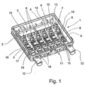
- Fig. 1 shows, in a perspective view, a
housing 1 of a connecting box without a lid. Thehousing 1 comprises aperipheral edge 2 and abase board 3. Anopening 5 is introduced into thebase board 3 so as to join aback edge region 4. Sixconductor rails 6 are arranged on thebase board 3. Two to sixconductor rails 6 may be arranged depending on the construction. Arespective cover 7 is provided on fiveconductor rails 6. Oneconductor rail 6, arranged next to a right-hand side wall 8, is shown without thecover 7. Oneconductor rail 6 comprises afirst contact element 9 and, opposite, asecond contact element 10. Thefirst contact elements 9 of theconductor rails 6 are associated with aconnection side 11 of thehousing 1. Thesecond contact elements 10 of theconductor rails 6 are associated with theopening 5. Theconductor rails 6 are arranged parallel and side by side.Contact terminals 12 are arranged on theconnection side 11 of thehousing 1. Thecontact terminals 12 are either constructed as contact connectors or as contact sockets. The twocontact terminals 12 are each directly electrically connected to thefirst contact elements 9 of theouter conductor rails 6. - The
second contact elements 10 are surrounded by acontact cage 13. Thesecond contact elements 10 are associated with openings of awall 14 used for feeding electric lines of the solar panel. Thewall 14 is guided so as to adjoin the opening 5 over the entire width of thehousing 1. -
Holding devices 15, into which theconductor rails 6 are inserted, are provided on thebase board 3. Theholding devices 15 are also used to hold thecovers 7 and thecontact cages 13. - The
contact cages 13 haveinsertion openings 16 facing theconductor rails 6 and into which thesecond contact elements 10 are inserted in thecontact cage 13. - Each
cover 7 has anupper side 17 which is substantially rectangular in construction and is arranged along the longitudinal direction of theconductor rail 6. Theupper side 17 hasside walls 18 arranged to be angled downwards at the side and inserted into the holdingdevices 15. Contactopenings 19 are located on theupper side 17. Thecontact openings 19 are arranged over contact regions of theconductor rails 6 and can therefore be contacted through thecover 7. Theupper side 17 is substantially constructed as a flat face. The upper sides of thecovers 7 are preferably arranged on approximately the same plane. Theupper sides 17 therefore form a relatively large overall bearing surface for a printed circuit board 20 (Fig. 2). - Fig. 2 shows the connecting box of Fig. 1 comprising a printed
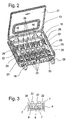
circuit board 20 and alid 21. The printedcircuit board 20 comprisescomponents 22 which are assembled on the printedcircuit board 20 and connected by electrical terminals toconductor paths 23 of the printedcircuit board 20. Theconductor paths 23 produce an electrical connection between thecomponents 20 andterminal pins 24 which are arranged on the lower side of the printedcircuit board 20 and are thus not visible in Fig. 2. The terminal pins 24 are guided through thecontact openings 19 in the contact regions of theconductor rails 6 and therefore produce an electrical connection between theconductor rails 6 and thecomponents 22. Diodes are preferably used ascomponents 22, which, depending on the embodiment and connection of the conductor rails, are connected to positive or negative lines of a solar panel and connect theconductor rails 6 to one another in a desired electrical function. The three right-hand conductor rails are connected in this example to electric lines of the solar panel which carry a positive voltage. The three lefthand conductor rails are connected in this embodiment to electric lines of the solar panel which carry a negative voltage. - The terminal pins 24 are arranged on the lower side of the printed circuit board and are electrically connected to the
conductor paths 23 via through-connections 25. In this embodiment the printedcircuit board 20 hasconnector elements 26 which are led out of the printedcircuit board 20 at a longitudinal side thereof and are inserted ininsertion openings 16 of thecontact cages 13. The width of theconnector elements 26 is adapted to the width of theinsertion openings 16 such that a spring loaded connection is produced between the printedcircuit board 20 and thecontact cages 13. In addition, the printedcircuit board 20 is located on theupper sides 17 of thecovers 7. Components which can be surface mounted (SMD) for example are used as thecomponents 22. - In contrast to the
housing 1 in Fig. 1, thehousing 1 of Fig. 2 comprisescable openings 28 via which the electric cable can be connected to the conductor rails 6. - Instead of the terminal pins 24, electric lines may also be provided.
- Fig. 3 shows a cross-section through
conductor rails 6 and the printedcircuit board 20. Theadhesive layer 27 in the form of a continuous adhesive layer is constructed between the printedcircuit board 20 and thecovers 7. The printedcircuit board 20 thus adheres to thecovers 7 which are in turn rigidly connected to thehousing 1 via the holdingdevices 15. Theadhesive layer 27 is preferably arranged only in the region of theupper sides 17. Theadhesive layer 27 can be constructed as a heat conducting layer, depending on the embodiment. In a further embodiment theadhesive layer 27 is produced by a preferably heat conducting adhesive foil. - Fig. 4 shows the printed circuit board of Fig. 2, the
adhesive layer 27 being provided on the lower side of the printedcircuit board 20 on which the terminal pins 24 are also arranged with which an electrical connection is made between thecomponents 22 of the printedcircuit board 20 and the conductor rails 6. In the process the terminal pins 24 are inserted through thecontact openings 19 of thecovers 7 incontact regions 30 of the conductor rails 6. - Fig. 5 shows, in a perspective view, a
conductor rail 6 comprising a first and asecond contact element conductor rail 6 has fourcontact regions 30 which are arranged between the first and thesecond contact element respective contact regions 30 are associated with the first orsecond contact element contact region 30 is illustrated in the embodiment shown by a spring clip. - Fig. 6 shows a detail of a further embodiment of a printed
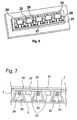
circuit board 20 in which thecomponents 22 are arranged on the lower side of the printedcircuit board 20, like thepin contacts 29. Anadhesive layer 27 with which the printedcircuit board 20 is glued to thelid 21 in the assembled state, is constructed on the upper side of the printedcircuit board 20 in this embodiment. - Fig. 7 shows a cross-section through the
housing 1 of the printedcircuit board 20 of Fig. 6 assembled in the connecting box. In this embodiment thecomponents 22 are arranged between thecovers 7. Thepin contacts 29 are guided through thecontact openings 19 of thecovers 7 into thecontact regions 30. Theadhesive layer 27, which is glued to thelid 21, is formed on the upper side of the printedcircuit board 20. - The printed
circuit board 20 can be constructed as a rigid or flexible printed circuit board, depending on the embodiment. The printed circuit board can be latched, screwed or caulked for holding purposes.
Claims (9)
- Connecting box for connecting to a solar panel comprising a housing (1) in which an opening (5) is provided for feeding electric lines of the solar panel, comprising contact elements (10) for connecting to the electric lines, comprising electrical components (22) which are connected to the contact elements (10), characterised in that the components (22) are arranged on a printed circuit board (20) and in that the printed circuit board (20) is held in the housing (1).
- Connecting box according to claim 1, characterised in that a contact element (13) comprises a holding recess (16), in that the printed circuit board (20) comprises a holding element (26), in that the holding element (26) is inserted in the holding recess (16) and holds the printed circuit board (20).
- Connecting box according to either claim 1 or claim 2, characterised in that the printed circuit board (20) is held in the connecting box by an adhesive layer (27).
- Connecting box according to claim 3, characterised in that the adhesive layer (27) is heat conducting.
- Connecting box according to either claim 3 or claim 4, characterised in that an adhesive foil is arranged as the adhesive layer (27).
- Connecting box according to any one of claims 3 to 5, characterised in that the adhesive layer (27) is arranged between the printed circuit board (20) and the housing (21).
- Connecting box according to any one of claims 3 to 5, characterised in that the adhesive layer (27) is arranged between the printed circuit board (20) and the contact elements (6).
- Connecting box according to any one of claims 1 to 7, characterised in that a plurality of contact elements (6) are arranged side-by-side, in that the contact elements (6) are covered by a cover (7), in that the cover (7) comprises an opening (19) for contacting the contact elements (6), in that the cover (7) comprises a bearing surface (17) for carrying the printed circuit board (20), in that the printed circuit board (20) rests on the bearing surface (17) of the cover (7), and in that lines (24) of the printed circuit board (20) are guided through the opening to the contact elements (6).
- Connecting box according to any one of claims 1 to 8, characterised in that the components (22) are arranged on the lower side of the printed circuit board (20), and in that the components (22) are arranged between the contact elements (6).
Applications Claiming Priority (2)
| Application Number | Priority Date | Filing Date | Title |
|---|---|---|---|
| DE20311184U DE20311184U1 (en) | 2003-07-21 | 2003-07-21 | Junction box for connection to a solar panel |
| DE20311184U | 2003-07-21 |
Publications (2)
| Publication Number | Publication Date |
|---|---|
| EP1501133A1 true EP1501133A1 (en) | 2005-01-26 |
| EP1501133B1 EP1501133B1 (en) | 2006-09-13 |
Family
ID=31896522
Family Applications (1)
| Application Number | Title | Priority Date | Filing Date |
|---|---|---|---|
| EP04015562A Not-in-force EP1501133B1 (en) | 2003-07-21 | 2004-07-02 | Connecting box for connecting to a solar panel |
Country Status (7)
| Country | Link |
|---|---|
| US (1) | US7134883B2 (en) |
| EP (1) | EP1501133B1 (en) |
| JP (1) | JP2005045255A (en) |
| CN (1) | CN100541949C (en) |
| AT (1) | ATE339775T1 (en) |
| DE (2) | DE20311184U1 (en) |
| ES (1) | ES2273130T3 (en) |
Cited By (4)
| Publication number | Priority date | Publication date | Assignee | Title |
|---|---|---|---|---|
| EP1729348A2 (en) | 2005-06-03 | 2006-12-06 | Günther Spelsberg GmbH & Co. KG | Junction box for a solar cell modul |
| WO2008066764A1 (en) * | 2006-11-22 | 2008-06-05 | Tyco Electronics Corporation | Heat dissipation system for photovoltaic array interconnection sytem |
| DE202007019048U1 (en) | 2007-04-13 | 2010-05-12 | Huber + Suhner Ag | junction box |
| EP2645504A2 (en) | 2006-06-29 | 2013-10-02 | Huber+Suhner AG | Connection box |
Families Citing this family (68)
| Publication number | Priority date | Publication date | Assignee | Title |
|---|---|---|---|---|
| JP2005303049A (en) * | 2004-04-13 | 2005-10-27 | Sumitomo Wiring Syst Ltd | Terminal box for solar cell module |
| DE102004020958B3 (en) * | 2004-04-28 | 2005-08-25 | Rose Systemtechnik Gmbh | Connection clip for cables, used e.g. in terminal blocks or on circuit boards, includes spring connections in differing configurations at either end of conductor strip |
| JP3744531B1 (en) * | 2004-05-07 | 2006-02-15 | 住友電装株式会社 | Terminal box for solar cell module and rectifying element unit |
| JP4515817B2 (en) * | 2004-05-18 | 2010-08-04 | 株式会社三社電機製作所 | Solar cell module connector |
| DE102004025627A1 (en) * | 2004-05-25 | 2005-12-22 | Tyco Electronics Amp Gmbh | Solar module with connection element |
| CN100479199C (en) * | 2005-01-14 | 2009-04-15 | 马尔遆公开股份有限公司 | Connection box for a solar panel and solar panel comprising a connection box |
| DE102005024644A1 (en) | 2005-05-25 | 2006-11-30 | G. Spelsberg Gmbh & Co. Kg | Electrical connection and connection box |
| DE102005025632B4 (en) * | 2005-06-03 | 2015-09-17 | Te Connectivity Germany Gmbh | Connecting device for connecting electrical foil conductors |
| JP2007110031A (en) * | 2005-10-17 | 2007-04-26 | Oonanba Kk | Terminal box for solar cell panel |
| DE102005050314A1 (en) * | 2005-10-20 | 2007-04-26 | Tyco Electronics Amp Gmbh | Connecting device for connecting an electrical conductor to a connecting line with a diode component |
| DE102007027861A1 (en) * | 2006-10-04 | 2008-04-10 | Günther Spelsberg GmbH & Co. KG | Assembly set for electrical socket i.e. connection box for solar cell module, has cable carrier for carrying cable, and cover provided for closing housing, where cover is arranged such that inner area of housing is accessible |
| US7291036B1 (en) * | 2006-11-08 | 2007-11-06 | Tyco Electronics Corporation | Photovoltaic connection system |
| US20080110490A1 (en) * | 2006-11-15 | 2008-05-15 | Tyco Electronics Corporation | Photovoltaic connection system |
| DE102006056259A1 (en) | 2006-11-27 | 2008-05-29 | Kostal Industrie Elektrik Gmbh | Electrical circuit board with a connection terminal |
| JP5441716B2 (en) | 2007-02-05 | 2014-03-12 | フェニックス コンタクト ゲーエムベーハー ウント コムパニー カーゲー | Connection box for photovoltaic modules |
| US8033859B2 (en) | 2007-02-05 | 2011-10-11 | Phoenix Contact Gmbh & Co. Kg | Connection and junction box for a solar module |
| US7762832B2 (en) | 2007-02-12 | 2010-07-27 | Minnick Jamie J | Systems for providing electrical interconnection between solar modules |
| DE202007005126U1 (en) * | 2007-04-04 | 2008-08-14 | Weidmüller Interface GmbH & Co. KG | Electrical connection device for contacts, in particular blade contacts |
| US20080253092A1 (en) * | 2007-04-13 | 2008-10-16 | Tyco Electronics Corporation | Heat Dissipation System for Photovoltaic Interconnection System |
| US10468993B2 (en) * | 2007-05-17 | 2019-11-05 | Enphase Energy, Inc. | Inverter for use in photovoltaic module |
| DE102007043178A1 (en) * | 2007-09-11 | 2009-03-12 | Yamaichi Electronics Deutschland Gmbh | Junction box, solar panel, contact device and procedure |
| US20090084426A1 (en) * | 2007-09-28 | 2009-04-02 | Enphase Energy, Inc. | Universal interface for a photovoltaic module |
| US8222533B2 (en) * | 2007-10-02 | 2012-07-17 | Tyco Electronics Corporation | Low profile photovoltaic (LPPV) box |
| DE102008003448B4 (en) * | 2008-01-08 | 2017-01-05 | Yamaichi Electronics Deutschland Gmbh | Junction box, use, solar panel, contact element, and procedure |
| DE102008010026A1 (en) * | 2008-02-20 | 2009-08-27 | Kostal Industrie Elektrik Gmbh | Electrical connection and connection box for a solar cell module |
| DE102008022297B4 (en) * | 2008-03-13 | 2011-04-14 | Fpe Fischer Gmbh | Connection box for solar modules and method for mounting them on the modules |
| FR2928784A1 (en) * | 2008-03-14 | 2009-09-18 | Bertrand Courtaigne | Electric connection device for electric solar panel, has printed circuit board carrying electronic components such as diodes, where board is connected electrically on connection elements that are forcibly connected with conductors |
| US7833033B2 (en) * | 2008-04-16 | 2010-11-16 | Molex Incorporated | Solar panel junction box and components thereof |
| DE102008057078A1 (en) * | 2008-06-12 | 2009-12-17 | Anton Gensler Gmbh | Junction box for photovoltaic modules |
| DE102008028462A1 (en) | 2008-06-14 | 2009-12-17 | Kostal Industrie Elektrik Gmbh | Electrical connection and connection box for a solar cell module |
| US8113853B2 (en) * | 2008-08-29 | 2012-02-14 | Heyco, Inc. | Junction box for photovoltaic systems |
| US7914298B2 (en) * | 2008-10-10 | 2011-03-29 | Tyco Electronics Corporation | Solar box and two position solar connectors |
| DE102008062034B4 (en) * | 2008-12-12 | 2010-08-12 | Tyco Electronics Amp Gmbh | Connecting device for connection to a solar module and solar module with such a connection device |
| DE102009004100A1 (en) * | 2009-01-08 | 2010-07-15 | Yamaichi Electronics Deutschland Gmbh | Solar panel for generating electrical energy from sunlight, has electrical conductors sectionally arranged in recess and electrically connected by diode, and cover element fixed at connection side element and covering recess and diode |
| US8106295B1 (en) * | 2009-01-28 | 2012-01-31 | Taymac Corporation | Apparatus and method for collapsible and expandable electrical device cover |
| US8435056B2 (en) * | 2009-04-16 | 2013-05-07 | Enphase Energy, Inc. | Apparatus for coupling power generated by a photovoltaic module to an output |
| WO2010123325A2 (en) * | 2009-04-24 | 2010-10-28 | 커넥스일렉트로닉스(주) | Smart junction box for a solar cell module |
| DE102009022570A1 (en) * | 2009-05-25 | 2010-12-02 | Yamaichi Electronics Deutschland Gmbh | Junction box, solar panel and procedure |
| US7862383B2 (en) * | 2009-06-03 | 2011-01-04 | Tyco Electronics Corporation | Electrical connector for a solar module assembly |
| DE102009033481B4 (en) * | 2009-07-15 | 2012-07-05 | Phoenix Contact Gmbh & Co. Kg | Connection and connection device |
| WO2011031663A1 (en) * | 2009-09-11 | 2011-03-17 | First Solar, Inc. | Cord plate |
| DE102010002565B8 (en) * | 2010-03-04 | 2012-03-22 | Tyco Electronics Amp Gmbh | Connecting device for a solar module |
| CN102208783B (en) * | 2010-03-31 | 2014-04-02 | 富士康(昆山)电脑接插件有限公司 | Junction box |
| DE102010029714A1 (en) * | 2010-04-08 | 2011-10-13 | Tyco Electronics Amp Gmbh | Electrical spring clamp, punched grid, busbar and electrical connection device |
| CN101847796B (en) * | 2010-04-23 | 2012-10-17 | 苏州快可光伏电子股份有限公司 | Connecting terminal for solar terminal box |
| US9101082B1 (en) | 2010-05-03 | 2015-08-04 | Sunpower Corporation | Junction box thermal management |
| US9425734B2 (en) | 2010-07-12 | 2016-08-23 | Lumos Lsx, Llc | Junction cover for photovoltaic panel modules |
| US20120033392A1 (en) * | 2010-08-09 | 2012-02-09 | Tyco Electronics Corporation | Modular Junction Box for a Photovoltaic Module |
| CN201830173U (en) * | 2010-09-01 | 2011-05-11 | 富士康(昆山)电脑接插件有限公司 | Junction box |
| US8432699B2 (en) * | 2010-09-17 | 2013-04-30 | Delta Electronics, Inc. | Junction box and electrical connection mechanism thereof |
| DE102010045973B4 (en) * | 2010-09-18 | 2014-01-30 | Common Link Ag | Device for monitoring currents |
| US8388358B2 (en) * | 2010-09-28 | 2013-03-05 | Tyco Electronics Corporation | Contact rail for a junction box |
| WO2012083049A1 (en) | 2010-12-17 | 2012-06-21 | First Solar, Inc | Electrical connection system |
| US8907212B2 (en) * | 2011-07-05 | 2014-12-09 | Hon Hai Precision Industry Co., Ltd. | Junction box with improved heat dissipation |
| TWM422759U (en) * | 2011-07-11 | 2012-02-11 | Ampower Technology Co Ltd | Cooling structure for junction box |
| KR20140062039A (en) | 2011-07-18 | 2014-05-22 | 엔페이즈 에너지, 인코포레이티드 | Resilient mounting assembly for photovoltaic modules |
| JP5729648B2 (en) * | 2011-10-13 | 2015-06-03 | ホシデン株式会社 | Terminal box for solar cell module |
| TWM423402U (en) * | 2011-10-18 | 2012-02-21 | Ji-Ren Yang | Bus box |
| CN103137734B (en) * | 2011-11-24 | 2015-07-15 | 崔鹏 | Solar photovoltaic junction box |
| DE102012006033A1 (en) | 2012-03-27 | 2013-10-02 | Kostal Industrie Elektrik Gmbh | Electrical installation and connecting device for solar cell module, has connectors electrically connected to bus bars and partially received in housing that is designed as component of solar cell module comprising frame |
| CN104756261A (en) * | 2012-10-25 | 2015-07-01 | 韩国艾尼凯斯特有限公司 | Concentrated photovoltaic module including heat pipe |
| USD734653S1 (en) | 2012-11-09 | 2015-07-21 | Enphase Energy, Inc. | AC module mounting bracket |
| DE102013004693A1 (en) | 2013-03-19 | 2014-09-25 | Kostal Industrie Elektrik Gmbh | Electrical connection and connection device for a solar cell module |
| US20150003021A1 (en) * | 2013-06-29 | 2015-01-01 | Chicony Power Technology Co., Ltd. | Inverter module |
| USD777813S1 (en) * | 2013-08-15 | 2017-01-31 | Peer Ketterle | Connecting box for a control unit |
| CN205051644U (en) * | 2015-08-26 | 2016-02-24 | 泰科电子(上海)有限公司 | Photovoltaic junction box |
| CN106685339A (en) * | 2015-11-06 | 2017-05-17 | 泰科电子(上海)有限公司 | Photovoltaic junction box and diode |
| JP2020161233A (en) * | 2019-03-25 | 2020-10-01 | 矢崎総業株式会社 | connector |
Citations (5)
| Publication number | Priority date | Publication date | Assignee | Title |
|---|---|---|---|---|
| US5513075A (en) * | 1992-05-08 | 1996-04-30 | The Whitaker Corporation | Module for electrically connecting conductor wires to circuits of flat surfaces such as solar panels |
| EP0999601A1 (en) * | 1998-10-29 | 2000-05-10 | Sumitomo Wiring Systems, Ltd. | A terminal box device, and a solar panel and terminal box device assembly |
| EP1102354A2 (en) * | 1999-11-17 | 2001-05-23 | Tyco Electronics AMP GmbH | Apparatus for contacting foil conductors, in particular of a solar module |
| US6283769B1 (en) * | 1999-07-01 | 2001-09-04 | Sumitomo Wiring Systems, Ltd. | Electric connecting box |
| US6307515B1 (en) * | 1998-12-09 | 2001-10-23 | Saint-Gobain Vitrage | Contact device for an electrical functional element disposed on a window |
Family Cites Families (14)
| Publication number | Priority date | Publication date | Assignee | Title |
|---|---|---|---|---|
| US4310211A (en) * | 1979-12-26 | 1982-01-12 | Amp Incorporated | High current contact system for solar modules |
| US4460232A (en) * | 1982-05-24 | 1984-07-17 | Amp, Incorporated | Junction box for solar modules |
| US5280133A (en) * | 1991-12-13 | 1994-01-18 | United Solar Systems Corporation | Junction box for a solar panel |
| JPH11150287A (en) * | 1997-09-10 | 1999-06-02 | Canon Inc | Solar cell module, solar cell with enclosure, method for fitting enclosure with the solar cell, and solar power generating system |
| US6247258B1 (en) * | 1998-09-09 | 2001-06-19 | O'malley John | Topple resistant, modular and mobile signage system |
| JP3785276B2 (en) * | 1998-09-10 | 2006-06-14 | 矢崎総業株式会社 | Electrical junction box |
| WO2000030216A1 (en) * | 1998-11-17 | 2000-05-25 | Utilux Pty. Limited | Solar panel cable connector |
| DE60039019D1 (en) * | 1999-11-17 | 2008-07-10 | Tyco Electronics Amp Gmbh | Device for connecting conductor foils, in particular a solar module |
| JP3457239B2 (en) * | 1999-11-24 | 2003-10-14 | 株式会社オートネットワーク技術研究所 | Circuit forming method and circuit connection structure in electrical junction box |
| JP2001308361A (en) * | 2000-04-24 | 2001-11-02 | Sanyo Electric Co Ltd | Solar cell module |
| US6543940B2 (en) * | 2001-04-05 | 2003-04-08 | Max Chu | Fiber converter faceplate outlet |
| JP2003052185A (en) * | 2001-05-30 | 2003-02-21 | Canon Inc | Power converter, and photovoltaic element module using the same and power generator |
| JP2002359389A (en) * | 2001-05-31 | 2002-12-13 | Kitani Denki Kk | Terminal box for solar power generation module wiring |
| DE20113643U1 (en) * | 2001-08-17 | 2001-11-29 | Stadtfeld Elektrotechnische Fa | Installation block for a cable junction box |
-
2003
- 2003-07-21 DE DE20311184U patent/DE20311184U1/en not_active Expired - Lifetime
-
2004
- 2004-07-02 AT AT04015562T patent/ATE339775T1/en active
- 2004-07-02 EP EP04015562A patent/EP1501133B1/en not_active Not-in-force
- 2004-07-02 DE DE602004002344T patent/DE602004002344T2/en active Active
- 2004-07-02 ES ES04015562T patent/ES2273130T3/en active Active
- 2004-07-21 CN CNB2004100549104A patent/CN100541949C/en not_active Expired - Fee Related
- 2004-07-21 JP JP2004212906A patent/JP2005045255A/en active Pending
- 2004-07-21 US US10/895,495 patent/US7134883B2/en active Active
Patent Citations (5)
| Publication number | Priority date | Publication date | Assignee | Title |
|---|---|---|---|---|
| US5513075A (en) * | 1992-05-08 | 1996-04-30 | The Whitaker Corporation | Module for electrically connecting conductor wires to circuits of flat surfaces such as solar panels |
| EP0999601A1 (en) * | 1998-10-29 | 2000-05-10 | Sumitomo Wiring Systems, Ltd. | A terminal box device, and a solar panel and terminal box device assembly |
| US6307515B1 (en) * | 1998-12-09 | 2001-10-23 | Saint-Gobain Vitrage | Contact device for an electrical functional element disposed on a window |
| US6283769B1 (en) * | 1999-07-01 | 2001-09-04 | Sumitomo Wiring Systems, Ltd. | Electric connecting box |
| EP1102354A2 (en) * | 1999-11-17 | 2001-05-23 | Tyco Electronics AMP GmbH | Apparatus for contacting foil conductors, in particular of a solar module |
Cited By (8)
| Publication number | Priority date | Publication date | Assignee | Title |
|---|---|---|---|---|
| EP1729348A2 (en) | 2005-06-03 | 2006-12-06 | Günther Spelsberg GmbH & Co. KG | Junction box for a solar cell modul |
| EP1729348A3 (en) * | 2005-06-03 | 2008-12-31 | Günther Spelsberg GmbH & Co. KG | Junction box for a solar cell modul |
| EP2645504A2 (en) | 2006-06-29 | 2013-10-02 | Huber+Suhner AG | Connection box |
| EP2645504A3 (en) * | 2006-06-29 | 2014-08-27 | Huber+Suhner AG | Connection box |
| WO2008066764A1 (en) * | 2006-11-22 | 2008-06-05 | Tyco Electronics Corporation | Heat dissipation system for photovoltaic array interconnection sytem |
| DE202007019048U1 (en) | 2007-04-13 | 2010-05-12 | Huber + Suhner Ag | junction box |
| US7811098B2 (en) | 2007-04-13 | 2010-10-12 | Huber + Suhner Ag | Connecting box of a solar panel with a cooling structure |
| US7880098B2 (en) | 2007-04-13 | 2011-02-01 | Hubert + Suhner Ag | Connecting box of a solar panel with a cooling structure |
Also Published As
| Publication number | Publication date |
|---|---|
| US20050054219A1 (en) | 2005-03-10 |
| EP1501133B1 (en) | 2006-09-13 |
| US7134883B2 (en) | 2006-11-14 |
| JP2005045255A (en) | 2005-02-17 |
| DE602004002344T2 (en) | 2007-09-20 |
| ES2273130T3 (en) | 2007-05-01 |
| DE20311184U1 (en) | 2004-02-19 |
| ATE339775T1 (en) | 2006-10-15 |
| DE602004002344D1 (en) | 2006-10-26 |
| CN1578035A (en) | 2005-02-09 |
| CN100541949C (en) | 2009-09-16 |
Similar Documents
| Publication | Publication Date | Title |
|---|---|---|
| EP1501133A1 (en) | Connecting box for connecting to a solar panel | |
| US7097516B2 (en) | Connecting box for a solar panel and solar panel | |
| US7833033B2 (en) | Solar panel junction box and components thereof | |
| US3731254A (en) | Jumper for interconnecting dual-in-line sockets | |
| US20170012269A1 (en) | Connector For Connecting Cellular Electrical Elements And Method For Installing Such A Connector On A Battery Unit | |
| US5138528A (en) | Electrical packaging system and components therefor | |
| CN109792027B (en) | Connection module | |
| ATE311679T1 (en) | MODULAR ELECTRICAL CONNECTOR AND CONNECTION SYSTEM | |
| CA2248712A1 (en) | High density connector arrangement for a circuit board module | |
| US9160086B2 (en) | Electrical connectors for use with printed circuit boards | |
| US20130084726A1 (en) | Terminal unit having fused combiner/distribution bus bar assembly | |
| JPH06223895A (en) | Connector and its method | |
| EP2569809A2 (en) | Connector assembly for a photovoltaic module | |
| DE60043637D1 (en) | Electrical connector with holding means for releasably fixing a component package | |
| GB1209158A (en) | Device for testing experimental circuits | |
| JP2020061273A (en) | Bus bar module and assembly method of bus bar module | |
| JP2000068547A (en) | Solar battery module terminal box and wiring system using the same | |
| CN214313623U (en) | Socket, socket unit, inspection tool, and inspection tool unit | |
| CN116457990A (en) | Wiring module | |
| US3907397A (en) | High density connector plug assembly | |
| US6520810B1 (en) | Connector system for interconnection with flat flexible circuitry | |
| PL179227B1 (en) | Interface unit | |
| US4557541A (en) | Apparatus for connecting cables to printed circuit boards | |
| US6261124B1 (en) | Connectors | |
| FI85932B (en) | ELECTRIC EQUIPMENT. |
Legal Events
| Date | Code | Title | Description |
|---|---|---|---|
| PUAI | Public reference made under article 153(3) epc to a published international application that has entered the european phase |
Free format text: ORIGINAL CODE: 0009012 |
|
| AK | Designated contracting states |
Kind code of ref document: A1 Designated state(s): AT BE BG CH CY CZ DE DK EE ES FI FR GB GR HU IE IT LI LU MC NL PL PT RO SE SI SK TR |
|
| AX | Request for extension of the european patent |
Extension state: AL HR LT LV MK |
|
| 17P | Request for examination filed |
Effective date: 20050514 |
|
| 17Q | First examination report despatched |
Effective date: 20050616 |
|
| AKX | Designation fees paid |
Designated state(s): AT BE BG CH CY CZ DE DK EE ES FI FR GB GR HU IE IT LI LU MC NL PL PT RO SE SI SK TR |
|
| GRAP | Despatch of communication of intention to grant a patent |
Free format text: ORIGINAL CODE: EPIDOSNIGR1 |
|
| GRAS | Grant fee paid |
Free format text: ORIGINAL CODE: EPIDOSNIGR3 |
|
| GRAA | (expected) grant |
Free format text: ORIGINAL CODE: 0009210 |
|
| AK | Designated contracting states |
Kind code of ref document: B1 Designated state(s): AT BE BG CH CY CZ DE DK EE ES FI FR GB GR HU IE IT LI LU MC NL PL PT RO SE SI SK TR |
|
| PG25 | Lapsed in a contracting state [announced via postgrant information from national office to epo] |
Ref country code: IT Free format text: LAPSE BECAUSE OF FAILURE TO SUBMIT A TRANSLATION OF THE DESCRIPTION OR TO PAY THE FEE WITHIN THE PRESCRIBED TIME-LIMIT;WARNING: LAPSES OF ITALIAN PATENTS WITH EFFECTIVE DATE BEFORE 2007 MAY HAVE OCCURRED AT ANY TIME BEFORE 2007. THE CORRECT EFFECTIVE DATE MAY BE DIFFERENT FROM THE ONE RECORDED. Effective date: 20060913 Ref country code: CZ Free format text: LAPSE BECAUSE OF FAILURE TO SUBMIT A TRANSLATION OF THE DESCRIPTION OR TO PAY THE FEE WITHIN THE PRESCRIBED TIME-LIMIT Effective date: 20060913 Ref country code: CH Free format text: LAPSE BECAUSE OF FAILURE TO SUBMIT A TRANSLATION OF THE DESCRIPTION OR TO PAY THE FEE WITHIN THE PRESCRIBED TIME-LIMIT Effective date: 20060913 Ref country code: BE Free format text: LAPSE BECAUSE OF FAILURE TO SUBMIT A TRANSLATION OF THE DESCRIPTION OR TO PAY THE FEE WITHIN THE PRESCRIBED TIME-LIMIT Effective date: 20060913 Ref country code: RO Free format text: LAPSE BECAUSE OF FAILURE TO SUBMIT A TRANSLATION OF THE DESCRIPTION OR TO PAY THE FEE WITHIN THE PRESCRIBED TIME-LIMIT Effective date: 20060913 Ref country code: PL Free format text: LAPSE BECAUSE OF FAILURE TO SUBMIT A TRANSLATION OF THE DESCRIPTION OR TO PAY THE FEE WITHIN THE PRESCRIBED TIME-LIMIT Effective date: 20060913 Ref country code: LI Free format text: LAPSE BECAUSE OF FAILURE TO SUBMIT A TRANSLATION OF THE DESCRIPTION OR TO PAY THE FEE WITHIN THE PRESCRIBED TIME-LIMIT Effective date: 20060913 Ref country code: SK Free format text: LAPSE BECAUSE OF FAILURE TO SUBMIT A TRANSLATION OF THE DESCRIPTION OR TO PAY THE FEE WITHIN THE PRESCRIBED TIME-LIMIT Effective date: 20060913 Ref country code: SI Free format text: LAPSE BECAUSE OF FAILURE TO SUBMIT A TRANSLATION OF THE DESCRIPTION OR TO PAY THE FEE WITHIN THE PRESCRIBED TIME-LIMIT Effective date: 20060913 |
|
| REG | Reference to a national code |
Ref country code: GB Ref legal event code: FG4D |
|
| REG | Reference to a national code |
Ref country code: CH Ref legal event code: EP |
|
| REG | Reference to a national code |
Ref country code: IE Ref legal event code: FG4D |
|
| REF | Corresponds to: |
Ref document number: 602004002344 Country of ref document: DE Date of ref document: 20061026 Kind code of ref document: P |
|
| PG25 | Lapsed in a contracting state [announced via postgrant information from national office to epo] |
Ref country code: SE Free format text: LAPSE BECAUSE OF FAILURE TO SUBMIT A TRANSLATION OF THE DESCRIPTION OR TO PAY THE FEE WITHIN THE PRESCRIBED TIME-LIMIT Effective date: 20061213 Ref country code: BG Free format text: LAPSE BECAUSE OF FAILURE TO SUBMIT A TRANSLATION OF THE DESCRIPTION OR TO PAY THE FEE WITHIN THE PRESCRIBED TIME-LIMIT Effective date: 20061213 Ref country code: DK Free format text: LAPSE BECAUSE OF FAILURE TO SUBMIT A TRANSLATION OF THE DESCRIPTION OR TO PAY THE FEE WITHIN THE PRESCRIBED TIME-LIMIT Effective date: 20061213 |
|
| PG25 | Lapsed in a contracting state [announced via postgrant information from national office to epo] |
Ref country code: PT Free format text: LAPSE BECAUSE OF FAILURE TO SUBMIT A TRANSLATION OF THE DESCRIPTION OR TO PAY THE FEE WITHIN THE PRESCRIBED TIME-LIMIT Effective date: 20070226 |
|
| ET | Fr: translation filed | ||
| REG | Reference to a national code |
Ref country code: CH Ref legal event code: PL |
|
| REG | Reference to a national code |
Ref country code: ES Ref legal event code: FG2A Ref document number: 2273130 Country of ref document: ES Kind code of ref document: T3 |
|
| PLBE | No opposition filed within time limit |
Free format text: ORIGINAL CODE: 0009261 |
|
| STAA | Information on the status of an ep patent application or granted ep patent |
Free format text: STATUS: NO OPPOSITION FILED WITHIN TIME LIMIT |
|
| 26N | No opposition filed |
Effective date: 20070614 |
|
| PG25 | Lapsed in a contracting state [announced via postgrant information from national office to epo] |
Ref country code: MC Free format text: LAPSE BECAUSE OF NON-PAYMENT OF DUE FEES Effective date: 20070731 Ref country code: GR Free format text: LAPSE BECAUSE OF FAILURE TO SUBMIT A TRANSLATION OF THE DESCRIPTION OR TO PAY THE FEE WITHIN THE PRESCRIBED TIME-LIMIT Effective date: 20061214 |
|
| PG25 | Lapsed in a contracting state [announced via postgrant information from national office to epo] |
Ref country code: EE Free format text: LAPSE BECAUSE OF FAILURE TO SUBMIT A TRANSLATION OF THE DESCRIPTION OR TO PAY THE FEE WITHIN THE PRESCRIBED TIME-LIMIT Effective date: 20060913 |
|
| PG25 | Lapsed in a contracting state [announced via postgrant information from national office to epo] |
Ref country code: IE Free format text: LAPSE BECAUSE OF NON-PAYMENT OF DUE FEES Effective date: 20070702 |
|
| PGRI | Patent reinstated in contracting state [announced from national office to epo] |
Ref country code: IT Effective date: 20081001 |
|
| PG25 | Lapsed in a contracting state [announced via postgrant information from national office to epo] |
Ref country code: CY Free format text: LAPSE BECAUSE OF FAILURE TO SUBMIT A TRANSLATION OF THE DESCRIPTION OR TO PAY THE FEE WITHIN THE PRESCRIBED TIME-LIMIT Effective date: 20060913 Ref country code: LU Free format text: LAPSE BECAUSE OF NON-PAYMENT OF DUE FEES Effective date: 20070702 |
|
| PG25 | Lapsed in a contracting state [announced via postgrant information from national office to epo] |
Ref country code: TR Free format text: LAPSE BECAUSE OF FAILURE TO SUBMIT A TRANSLATION OF THE DESCRIPTION OR TO PAY THE FEE WITHIN THE PRESCRIBED TIME-LIMIT Effective date: 20060913 Ref country code: HU Free format text: LAPSE BECAUSE OF FAILURE TO SUBMIT A TRANSLATION OF THE DESCRIPTION OR TO PAY THE FEE WITHIN THE PRESCRIBED TIME-LIMIT Effective date: 20070314 |
|
| REG | Reference to a national code |
Ref country code: FR Ref legal event code: PLFP Year of fee payment: 12 |
|
| REG | Reference to a national code |
Ref country code: DE Ref legal event code: R082 Ref document number: 602004002344 Country of ref document: DE Representative=s name: WILHELM & BECK, DE Ref country code: DE Ref legal event code: R081 Ref document number: 602004002344 Country of ref document: DE Owner name: TE CONNECTIVITY GERMANY GMBH, DE Free format text: FORMER OWNER: TYCO ELECTRONICS AMP GMBH, 64625 BENSHEIM, DE |
|
| REG | Reference to a national code |
Ref country code: FR Ref legal event code: CD Owner name: TE CONNECTIVITY GERMANY GMBH Effective date: 20151027 |
|
| REG | Reference to a national code |
Ref country code: NL Ref legal event code: HC Owner name: TE CONNECTIVITY GERMANY GMBH; DE Free format text: DETAILS ASSIGNMENT: VERANDERING VAN EIGENAAR(S), VERANDERING VAN NAAM VAN DE EIGENAAR(S); FORMER OWNER NAME: TYCO ELECTRONICS AMP GMBH Effective date: 20150930 |
|
| REG | Reference to a national code |
Ref country code: AT Ref legal event code: HC Ref document number: 339775 Country of ref document: AT Kind code of ref document: T Owner name: TE CONNECTIVITY GERMANY GMBH, DE Effective date: 20160321 |
|
| REG | Reference to a national code |
Ref country code: FR Ref legal event code: PLFP Year of fee payment: 13 |
|
| REG | Reference to a national code |
Ref country code: FR Ref legal event code: PLFP Year of fee payment: 14 |
|
| REG | Reference to a national code |
Ref country code: FR Ref legal event code: PLFP Year of fee payment: 15 |
|
| PGFP | Annual fee paid to national office [announced via postgrant information from national office to epo] |
Ref country code: FR Payment date: 20200611 Year of fee payment: 17 |
|
| PGFP | Annual fee paid to national office [announced via postgrant information from national office to epo] |
Ref country code: GB Payment date: 20200624 Year of fee payment: 17 Ref country code: NL Payment date: 20200615 Year of fee payment: 17 |
|
| PGFP | Annual fee paid to national office [announced via postgrant information from national office to epo] |
Ref country code: ES Payment date: 20200803 Year of fee payment: 17 Ref country code: FI Payment date: 20200709 Year of fee payment: 17 Ref country code: DE Payment date: 20200617 Year of fee payment: 17 |
|
| PGFP | Annual fee paid to national office [announced via postgrant information from national office to epo] |
Ref country code: AT Payment date: 20200625 Year of fee payment: 17 Ref country code: IT Payment date: 20200610 Year of fee payment: 17 |
|
| REG | Reference to a national code |
Ref country code: DE Ref legal event code: R119 Ref document number: 602004002344 Country of ref document: DE |
|
| REG | Reference to a national code |
Ref country code: FI Ref legal event code: MAE |
|
| REG | Reference to a national code |
Ref country code: NL Ref legal event code: MM Effective date: 20210801 |
|
| REG | Reference to a national code |
Ref country code: AT Ref legal event code: MM01 Ref document number: 339775 Country of ref document: AT Kind code of ref document: T Effective date: 20210702 |
|
| GBPC | Gb: european patent ceased through non-payment of renewal fee |
Effective date: 20210702 |
|
| PG25 | Lapsed in a contracting state [announced via postgrant information from national office to epo] |
Ref country code: GB Free format text: LAPSE BECAUSE OF NON-PAYMENT OF DUE FEES Effective date: 20210702 Ref country code: FI Free format text: LAPSE BECAUSE OF NON-PAYMENT OF DUE FEES Effective date: 20210702 Ref country code: DE Free format text: LAPSE BECAUSE OF NON-PAYMENT OF DUE FEES Effective date: 20220201 Ref country code: AT Free format text: LAPSE BECAUSE OF NON-PAYMENT OF DUE FEES Effective date: 20210702 |
|
| PG25 | Lapsed in a contracting state [announced via postgrant information from national office to epo] |
Ref country code: NL Free format text: LAPSE BECAUSE OF NON-PAYMENT OF DUE FEES Effective date: 20210801 Ref country code: FR Free format text: LAPSE BECAUSE OF NON-PAYMENT OF DUE FEES Effective date: 20210731 |
|
| PG25 | Lapsed in a contracting state [announced via postgrant information from national office to epo] |
Ref country code: IT Free format text: LAPSE BECAUSE OF FAILURE TO SUBMIT A TRANSLATION OF THE DESCRIPTION OR TO PAY THE FEE WITHIN THE PRESCRIBED TIME-LIMIT Effective date: 20210702 |
|
| REG | Reference to a national code |
Ref country code: ES Ref legal event code: FD2A Effective date: 20220826 |
|
| PG25 | Lapsed in a contracting state [announced via postgrant information from national office to epo] |
Ref country code: ES Free format text: LAPSE BECAUSE OF NON-PAYMENT OF DUE FEES Effective date: 20210703 |