EP1729344A2 - Indikator für den ersten Chip eines IC wafers - Google Patents
Indikator für den ersten Chip eines IC wafers Download PDFInfo
- Publication number
- EP1729344A2 EP1729344A2 EP06076049A EP06076049A EP1729344A2 EP 1729344 A2 EP1729344 A2 EP 1729344A2 EP 06076049 A EP06076049 A EP 06076049A EP 06076049 A EP06076049 A EP 06076049A EP 1729344 A2 EP1729344 A2 EP 1729344A2
- Authority
- EP
- European Patent Office
- Prior art keywords
- wafer
- fdi
- die
- metal layer
- inker
- Prior art date
- Legal status (The legal status is an assumption and is not a legal conclusion. Google has not performed a legal analysis and makes no representation as to the accuracy of the status listed.)
- Withdrawn
Links
Images




Classifications
-
- H—ELECTRICITY
- H10—SEMICONDUCTOR DEVICES; ELECTRIC SOLID-STATE DEVICES NOT OTHERWISE PROVIDED FOR
- H10W—GENERIC PACKAGES, INTERCONNECTIONS, CONNECTORS OR OTHER CONSTRUCTIONAL DETAILS OF DEVICES COVERED BY CLASS H10
- H10W46/00—Marks applied to devices, e.g. for alignment or identification
-
- H—ELECTRICITY
- H10—SEMICONDUCTOR DEVICES; ELECTRIC SOLID-STATE DEVICES NOT OTHERWISE PROVIDED FOR
- H10W—GENERIC PACKAGES, INTERCONNECTIONS, CONNECTORS OR OTHER CONSTRUCTIONAL DETAILS OF DEVICES COVERED BY CLASS H10
- H10W46/00—Marks applied to devices, e.g. for alignment or identification
- H10W46/101—Marks applied to devices, e.g. for alignment or identification characterised by the type of information, e.g. logos or symbols
-
- H—ELECTRICITY
- H10—SEMICONDUCTOR DEVICES; ELECTRIC SOLID-STATE DEVICES NOT OTHERWISE PROVIDED FOR
- H10W—GENERIC PACKAGES, INTERCONNECTIONS, CONNECTORS OR OTHER CONSTRUCTIONAL DETAILS OF DEVICES COVERED BY CLASS H10
- H10W46/00—Marks applied to devices, e.g. for alignment or identification
- H10W46/501—Marks applied to devices, e.g. for alignment or identification for use before dicing
-
- H—ELECTRICITY
- H10—SEMICONDUCTOR DEVICES; ELECTRIC SOLID-STATE DEVICES NOT OTHERWISE PROVIDED FOR
- H10W—GENERIC PACKAGES, INTERCONNECTIONS, CONNECTORS OR OTHER CONSTRUCTIONAL DETAILS OF DEVICES COVERED BY CLASS H10
- H10W46/00—Marks applied to devices, e.g. for alignment or identification
- H10W46/501—Marks applied to devices, e.g. for alignment or identification for use before dicing
- H10W46/507—Located in dummy chips or in reference chips
-
- H—ELECTRICITY
- H10—SEMICONDUCTOR DEVICES; ELECTRIC SOLID-STATE DEVICES NOT OTHERWISE PROVIDED FOR
- H10W—GENERIC PACKAGES, INTERCONNECTIONS, CONNECTORS OR OTHER CONSTRUCTIONAL DETAILS OF DEVICES COVERED BY CLASS H10
- H10W46/00—Marks applied to devices, e.g. for alignment or identification
- H10W46/601—Marks applied to devices, e.g. for alignment or identification for use after dicing
- H10W46/603—Formed on wafers or substrates before dicing and remaining on chips after dicing
Definitions
- the present invention is generally directed to an integrated circuit (IC) wafer and, more specifically, to a first die indicator for an IC wafer.
- IC integrated circuit
- an integrated circuit (IC) wafer includes a plurality of die and a first die indicator (FDI) formed on the wafer.
- the plurality of die include a first potentially good IC die and the FDI, which is detectable by a machine vision recognition system, provides a unique indication of the first potentially good die.
- the FDI may include a plurality of rings arranged in an arrowhead pattern. The rings may be formed in a metal layer, which may be IC interconnect metal and/or cap metal and/or solder metal.
- the FDI may further include a product name and a mask set name.
- Text of the product name and the mask set name may have a text height of at least about 100 microns, so as to be visually detectable by the machine vision recognition system.
- the FDI may be positioned along a flat side of the wafer at an end of the flat side.
- the FDI may further include an inker target that indicates ink dot placement for defective dies.
- the inker target is diamond-shaped.
- the wafer may be of virtually any size.
- a first die indicator is implemented on an integrated circuit (IC) wafer to facilitate the maintenance of first die integrity throughout various wafer process steps.
- IC integrated circuit
- a design feature is placed on each of the wafers, which is visually detectable with an unaided human eye and/or a machine vision recognition system.
- the FDI provides an indication as to which die processing should begin with.
- the die indicator can be utilized on a variety of different sized wafers, e.g., four inch, five inch, six inch and eight inch wafers, and may be implemented on bumped and non-bumped wafers.
- the FDI is a unique structure that is distinguishable by the human eye and/or machine vision recognition systems.
- prior first die indicator designs have been inadequate, have not provided a solution for packaged stepper products and have been unreliable and inconsistent from part to part, due to size, color and contrast variations.
- an FDI is placed on the IC wafer next to the first testable die location. The FDI feature allows a person to accurately setup a given machine vision recognition system to begin processing of the wafer at the correct location.
- the FDI consists of an arrowhead formed by circular patterns in the metal layers, i.e., IC interconnect metal, cap metal and solder metal levels, and may also include an inker target pattern.
- ID identification
- text for a product name and mask set name may also be readily added to the FDI (see Fig. 2B) on metal levels other than cap metal and solder metal levels.
- the text height should be approximately 200 ⁇ m high, with a width of approximately 33 ⁇ m. To allow readability, it is generally desirable that the text have at least 50 ⁇ m separation from all other data. In general, the text should not be smaller than about 100 ⁇ m high, to be useful. Text height constraints are set to provide more uniqueness to the FDI.
- all metal levels typically receive an FDI and a truncated field. This, in general, ensures that the fields are visually unique from all other fields. Further, truncation of only one metal level, in general, is not desirable.
- an inker target that may be, for example, a 20-mil diamond placed on the interconnect metal levels and/or the cap metal level.
- the inker target is utilized to visually indicate where an operator should setup ink dot placements on defective die.
- the inker target diamond is part of the standard FDI pattern.
- the placement of the FDI pattern is relative to the inker target.
- the inker target is placed in the center of the die, with the exception of die that have internal solder metal in that area. When this occurs, it is desirable to move to a location away from the solder metal.
- the test area will designate a different location for the inker target, or a size and design of the inker target may be changed. It is generally desirable to place the inker targets away from internal solder metal, due to the fact that the solder metal bumps wick away the ink and, thus, a defective die may appear to be a good non-defective die.
- the metal bond pad shorting pattern is not utilized on eight inch wafers, or bump only wafers with interconnect metal levels on stepper reticles. All bump wafers may include cap metal shorting bars around the perimeter of the FDI die.
- a cap metal test die is used to visually inspect the cap metal etch process during fabrication.
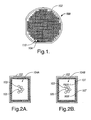
- a wafer array 100 includes a plurality of die 102, with a first die indicator (FDI) 104 located physically adjacent to the first potentially good die on the wafer array 100.
- the FDI 104 is positioned on the first whole die in the lower left position of the wafer array.
- exemplary FDI designs are shown.
- FDI 104A utilizes five circles 103, which form an arrowhead, and includes an inker target diamond 105.
- an FDI 104B also includes identification (ID) text 107.
- Fig. 3 depicts a relevant portion of an IC wafer array 100A that provides an FDI placement for projection and proximity aligners.
- the FDI 104 may be partially located in the 3mm keep out area by no more than about 25 percent or approximately about 750 ⁇ m. This allows the FDI 104 to remain inside the wafer array 100A an adequate amount, when a first level alignment error occurs.
- FIG. 4 an FDI placement for a 1X UT stepper aligner is depicted.
- the FDI 104 is placed on all interconnect metal levels and is positioned such that it is located in the 3mm keep out area by no more than 25 percent or approximately 750 ⁇ m. This is desirable to keep the FDI 104 inside wafer array 100B an adequate amount, when a first level alignment error occurs.
- Figs. 5 and 6 depict two set-up variations for an FDI placement on IC wafer arrays 100C and 100D for a 4X UT stepper aligner for a packaged IC or an IC set-up for package and bumping.
- the FDI 104 can fall into the 3mm keep out area by no more than 25 percent or approximately 750 ⁇ m, in order to maintain the FDI 104 inside the wafer arrays 100C and 100D by an adequate amount, when a first level alignment error occurs.
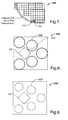
- Fig. 7 depicts a relevant portion of an IC wafer array 100E illustrating placement of the FDI 104 and cap test die 110 on a 4X UT stepper aligner for a metal bumped IC.
- Fig. 8 depicts an exemplary FDI 104C having a size of approximately 1250 ⁇ m by 1250 ⁇ m.
- the FDI 104C includes circles 103A and 103B and an inker target 105 having a dimension of approximately 400 ⁇ m by 400 ⁇ m.
- Fig. 9 corresponds to a view of the FDI 104C of Fig. 8 at an interconnect metal or cap metal level and
- Fig. 10 depicts the FDI 104C of Fig. 8 at a solder metal level.
- solder metal bumps are utilized to form the circles 103B, their outer diameter may be approximately 380 ⁇ m.
- an inner diameter of the circles 103A of the FDI may be approximately 360 ⁇ m.
- Fig. 11 depicts a top view of a relevant portion of an exemplary IC wafer array 200 including an FDI 104D having an ink target 105 formed in a cap metal level. As is shown, the die with the FDI 104D also includes shorting bars 112.
- Fig. 12 depicts a relevant portion of an IC wafer array 300 including an FDI 104E formed in a solder metal level.
- first die indicator has been described herein that may be advantageously implemented on an integrated circuit wafer to maintain first die integrity throughout various wafer processing steps.
Landscapes
- Testing Or Measuring Of Semiconductors Or The Like (AREA)
Applications Claiming Priority (1)
| Application Number | Priority Date | Filing Date | Title |
|---|---|---|---|
| US11/141,338 US7265567B2 (en) | 2005-05-31 | 2005-05-31 | First die indicator for integrated circuit wafer |
Publications (2)
| Publication Number | Publication Date |
|---|---|
| EP1729344A2 true EP1729344A2 (de) | 2006-12-06 |
| EP1729344A3 EP1729344A3 (de) | 2008-03-26 |
Family
ID=36778160
Family Applications (1)
| Application Number | Title | Priority Date | Filing Date |
|---|---|---|---|
| EP06076049A Withdrawn EP1729344A3 (de) | 2005-05-31 | 2006-05-15 | Indikator für den ersten Chip eines IC wafers |
Country Status (2)
| Country | Link |
|---|---|
| US (1) | US7265567B2 (de) |
| EP (1) | EP1729344A3 (de) |
Families Citing this family (4)
| Publication number | Priority date | Publication date | Assignee | Title |
|---|---|---|---|---|
| JP4837971B2 (ja) * | 2005-10-07 | 2011-12-14 | ルネサスエレクトロニクス株式会社 | 半導体装置の製造方法 |
| GB0903286D0 (en) * | 2009-02-26 | 2009-04-08 | Melexis Tessenderlo Nv | Testing integrated circuits |
| JP2012099670A (ja) * | 2010-11-02 | 2012-05-24 | Sumitomo Wiring Syst Ltd | 実装基板 |
| DE102015105752B4 (de) * | 2015-04-15 | 2021-08-05 | OSRAM Opto Semiconductors Gesellschaft mit beschränkter Haftung | Halbleiteranordnung mit Reservoir für Markermaterial |
Family Cites Families (14)
| Publication number | Priority date | Publication date | Assignee | Title |
|---|---|---|---|---|
| JPS61170041A (ja) * | 1985-01-23 | 1986-07-31 | Nec Corp | 半導体ウエ−ハ |
| JPS62114213A (ja) * | 1985-11-13 | 1987-05-26 | Nec Corp | 集積回路 |
| US5787174A (en) * | 1992-06-17 | 1998-07-28 | Micron Technology, Inc. | Remote identification of integrated circuit |
| JPH118328A (ja) * | 1997-06-17 | 1999-01-12 | Hitachi Ltd | 半導体装置およびその製造方法並びにその識別方法 |
| KR100307630B1 (ko) * | 1998-12-30 | 2001-09-28 | 윤종용 | 정렬 마크, 이를 사용하는 정렬 시스템 및 이를 이용한 정렬방법 |
| US6161213A (en) * | 1999-02-17 | 2000-12-12 | Icid, Llc | System for providing an integrated circuit with a unique identification |
| JP2002026041A (ja) * | 2000-07-12 | 2002-01-25 | Nec Machinery Corp | ダイボンダ |
| JP3671822B2 (ja) * | 2000-07-26 | 2005-07-13 | 株式会社日立製作所 | 欠陥検査方法および欠陥検査システム |
| US6701259B2 (en) * | 2000-10-02 | 2004-03-02 | Applied Materials, Inc. | Defect source identifier |
| US6717430B2 (en) * | 2002-02-13 | 2004-04-06 | Motorola, Inc. | Integrated circuit testing with a visual indicator |
| JP4126189B2 (ja) * | 2002-04-10 | 2008-07-30 | 株式会社日立ハイテクノロジーズ | 検査条件設定プログラム、検査装置および検査システム |
| JP2003324055A (ja) * | 2002-04-30 | 2003-11-14 | Canon Inc | 管理システム及び装置及び方法並びに露光装置及びその制御方法 |
| US7119351B2 (en) * | 2002-05-17 | 2006-10-10 | Gsi Group Corporation | Method and system for machine vision-based feature detection and mark verification in a workpiece or wafer marking system |
| US6812477B2 (en) * | 2002-12-04 | 2004-11-02 | Texas Instruments Incorporated | Integrated circuit identification |
-
2005
- 2005-05-31 US US11/141,338 patent/US7265567B2/en not_active Expired - Fee Related
-
2006
- 2006-05-15 EP EP06076049A patent/EP1729344A3/de not_active Withdrawn
Also Published As
| Publication number | Publication date |
|---|---|
| EP1729344A3 (de) | 2008-03-26 |
| US20060267617A1 (en) | 2006-11-30 |
| US7265567B2 (en) | 2007-09-04 |
Similar Documents
| Publication | Publication Date | Title |
|---|---|---|
| US6278193B1 (en) | Optical sensing method to place flip chips | |
| US5657394A (en) | Integrated circuit probe card inspection system | |
| US4985676A (en) | Method and apparatus of performing probing test for electrically and sequentially testing semiconductor device patterns | |
| US8372663B2 (en) | Good chip classifying method on wafer, and chip quality judging method, marking mechanism, and manufacturing method of semiconductor device using the good chip classifying method | |
| CN108122801B (zh) | 晶圆标记方法及晶圆标记系统 | |
| JP2013519227A (ja) | 多様な集積回路チップバンプピッチを有する半導体装置 | |
| US4914601A (en) | Method for profiling wafers and for locating dies thereon | |
| US7265567B2 (en) | First die indicator for integrated circuit wafer | |
| JP2010103543A (ja) | ボールグリッドアレイx線方位マーク | |
| JP2008539085A (ja) | レーザマーキングシステムにおけるウェハ処理システムを位置合わせするためのシステムおよび方法 | |
| US11493535B2 (en) | Systems and methods for depopulating pins from contactor test sockets for packaged semiconductor devices | |
| Marinissen et al. | Solutions to multiple probing challenges for test access to multi-die stacked integrated circuits | |
| EP0580895A2 (de) | Koordinatenvorgabe auf einer geprüften Halbleiterscheibe | |
| US12501542B2 (en) | Substrate with identification codes composed of identification pads | |
| US20060283012A1 (en) | Apparatus and method for solder ball placement | |
| US12543531B2 (en) | Substrate for carrying wafer | |
| US20080057677A1 (en) | Chip location identification | |
| US20070054514A1 (en) | Socket measurement apparatus and method | |
| JPS6247142A (ja) | 半導体装置のマ−キング法 | |
| JP2021012970A (ja) | 半導体装置およびその検査方法 | |
| KR0127639B1 (ko) | 프로우빙 시험 방법 및 그 장치 | |
| KR20180036195A (ko) | 웨이퍼 맵의 형성 방법 | |
| CN118983301A (zh) | 测试结构、失效定位方法以及失效分析方法 | |
| CN105580122A (zh) | 用于定位具有电子元器件的承载件的方法和以此类方法生产的电子元器件 | |
| JPS6170735A (ja) | 電気測定用アライメントマ−クを有するウエハまたはチツプ |
Legal Events
| Date | Code | Title | Description |
|---|---|---|---|
| PUAI | Public reference made under article 153(3) epc to a published international application that has entered the european phase |
Free format text: ORIGINAL CODE: 0009012 |
|
| AK | Designated contracting states |
Kind code of ref document: A2 Designated state(s): AT BE BG CH CY CZ DE DK EE ES FI FR GB GR HU IE IS IT LI LT LU LV MC NL PL PT RO SE SI SK TR |
|
| AX | Request for extension of the european patent |
Extension state: AL BA HR MK YU |
|
| PUAL | Search report despatched |
Free format text: ORIGINAL CODE: 0009013 |
|
| AK | Designated contracting states |
Kind code of ref document: A3 Designated state(s): AT BE BG CH CY CZ DE DK EE ES FI FR GB GR HU IE IS IT LI LT LU LV MC NL PL PT RO SE SI SK TR |
|
| AX | Request for extension of the european patent |
Extension state: AL BA HR MK YU |
|
| 17P | Request for examination filed |
Effective date: 20080926 |
|
| 17Q | First examination report despatched |
Effective date: 20081104 |
|
| AKX | Designation fees paid |
Designated state(s): AT BE BG CH CY CZ DE DK EE ES FI FR GB GR HU IE IS IT LI LT LU LV MC NL PL PT RO SE SI SK TR |
|
| STAA | Information on the status of an ep patent application or granted ep patent |
Free format text: STATUS: THE APPLICATION IS DEEMED TO BE WITHDRAWN |
|
| 18D | Application deemed to be withdrawn |
Effective date: 20090515 |